
 Open Access Article
 This Open Access Article is licensed under a Creative Commons Attribution-Non Commercial 3.0 Unported Licence
Solution-processed next generation thin film solar cells for indoor light applications
Snehangshu
Mishra
a,
Subrata
Ghosh
a,
Binita
Boro
b,
Dinesh
Kumar
a,
Shivam
Porwal
a,
Mrittika
Paul
a,
Himanshu
Dixit
a and
Trilok
Singh
 *ab
*ab
aFunctional Materials and Device Laboratory, School of Energy Science and Engineering, Indian Institute of Technology Kharagpur, 721302, West Bengal, India. E-mail: trilok@iitkgp.ac.in
bSchool of Nano Science and Technology, Indian Institute of Technology Kharagpur, 721302, West Bengal, India
First published on 30th September 2022
Abstract
Recently, indoor photovoltaics have gained research attention due to their potential applications in the Internet of Things (IoT) sector and most of the devices in modern technology are controlled via wireless/or battery-less means and powered by indoor photovoltaics. This review provides an overview of the developments of thin film solar cells, particularly solution-processed dye-sensitized solar cells, organic solar cells, quantum dot solar cells, and upcoming organic–inorganic metal halide perovskite solar cells for indoor applications. Further, a comprehensive material assessment, device design, and indoor lighting characteristics are discussed. We also highlight the challenges and prospects for the development of indoor photovoltaics for various IoT applications.
 Snehangshu Mishra | Snehangshu Mishra is currently pursuing PhD at the School of Energy Science and Engineering, Indian Institute of Technology Kharagpur, India since 2019. He received his BE degree in Electrical Engineering in 2015 and MTech degree in Energy Science and Technology in 2018 from Jadavpur University, Kolkata. His research interest is focused on development of low-cost flexible perovskite solar cells for indoor applications. |
 Subrata Ghosh | Dr Subrata Ghosh completed his BSc (in Industrial Chemistry) and MSc (in Applied Chemistry) at the University of Calcutta. Following his MSc degree, he joined the Indian Institute of Technology Bombay for his MTech program in Materials Science. During MTech, he extensively worked on developing Zirconia toughened alumina (ZTA) composites by solution process routes for structural applications. During his PhD in the School of Energy Science and Engineering, Indian Institute of Technology Kharagpur, he worked towards interfacial engineering and process modification for efficient and stable perovskite solar cells. He is currently working on large-area perovskite solar cell fabrication at the Indian Institute of Technology Kharagpur as a research associate. |
 Binita Boro | Binita Boro earned a BTech degree in Instrumentation Engineering from the Central Institute of Technology in Kokrajhar, Assam, and an MTech degree in advanced material science and technology from the National Institute of Technology in Durgapur, West Bengal She worked on “Improving the efficiency of Si solarcells using SiOx/TiO2 heterostructure nanowires based on antireflective coating” during her MTech. Currently, she is a doctoral student of School of Nanoscience and Technology, IIT Kharagpur. Her current research is focused on the interfaces of perovskite-based solar cells and how they affect device efficiency and stability. |
 Dinesh Kumar | Dinesh Kumar completed his bachelor's (in Physics) from the University of Delhi and his Master's Degree (in Condensed Matter Physics) from Banaras Hindu University. Following his Master's degree, he joined IIT Madras for his Master in Technology (in Functional Material and Nanotechnology). He has worked on the simulation study of crystalline-amorphous silicon-based tandem solar cells. He received Prime Minister's Research Fellowship (PMRF-2019) for his doctoral research. As a research scholar, he aims to work towards developing high-efficiency perovskite-based solar cells for multijunction, flexible, and PV system applications. |
 Shivam Porwal | Shivam Porwal completed his integrated MScTech in Materials Science and Engineering from Central Institute of Plastics Engineering and Technology, Bhubaneswar in 2016. Following this, he completed MTech in Materials Science and Technology from IIT BHU in 2019. He received Prime Minister's Research Fellowship (PMRF-2019) for his doctoral research. As a PhD candidate in Energy Science and Engineering, he aims to work towards the development of Perovskite solar cells. |
 Mrittika Paul | Mrittika Paul graduated from Vidyasagar University with a BSc in physics in 2017 and a MSc in physics in 2019. She worked on organic semiconducting materials that are employed in flexible electronics in her MSc project (from the Department of Physics, IIT Kharagpur). As a PhD candidate at the School of Energy Science and Engineering of IIT Kharagpur, she is working on all-inorganic perovskite solar cells. |
 Himanshu Dixit | Himanshu Dixit earned a BTech in electrical engineering from SKIT, Jaipur and an MTech in nanotechnology from Technical University, Kota Rajasthan. He worked on simulation, optimization, and characterization of perovskite solar cells during his MTech. He is currently pursuing PhD in Energy Science and Engineering at Indian Institute of Technology, Kharagpur. His current focus includes double perovskite-based solar cells and how to enhance their efficiency and stability. |
 Trilok Singh | Dr Trilok Singh is an assistant professor in the School of Energy Science and Engineering at the Indian Institute of Technology Kharagpur. He earned his PhD in Physics in 2012 from the Indian Institute of Technology in Delhi. He served as a postdoctoral researcher at the University of Cologne, Germany from 2011 to 2015 and then moved to Japan to avail international postdoctoral research fellowship through Japan Society for the Promotion of Science. He is the head of Functional Materials and Device Laboratory and his research group focuses on the development of smart energy generation and storage devices. |
1. Introduction
Ever since the industrial revolution, as human civilization progresses, the excessive emission of carbon dioxide from the industrial sector is continuously rising and it has presented humankind with the risk of global warming and climate change. Most of this emission comes from the energy generation using fossil fuels. As the energy demand is increasing rapidly day by day, the limited reserve of fossil fuels is depleting. In this scenario, renewable energy sources such as solar, wind, geothermal, and bio-energy are becoming more viable as these clean sources of energy can successfully substitute fossil fuels for electric power generation and can tackle the massive environmental problem of global warming. Over the years, continuous material developments have enabled various solar cell technologies to be highly efficient and low-cost energy alternatives. Solar power holds paramount promise as a renewable form of energy. The sun supplies a huge 173![[thin space (1/6-em)]](https://www.rsc.org/images/entities/char_2009.gif) 000 TW of energy per year and thus effective and efficient solar power utilization by solar photovoltaic systems presents a substantial solution for meeting the global energy demand.1
000 TW of energy per year and thus effective and efficient solar power utilization by solar photovoltaic systems presents a substantial solution for meeting the global energy demand.1
Recently, the Internet of Things (IoT) market has been growing unprecedentedly and is expected to be a multi-trillion-dollar market within a few years.2 IoT is defined as a system of interconnected objects, equipped with sensors, actuators, data storage devices, software, and other technologies, which can collect and transfer data without human interaction.3 In IoT, a wide range of sensors and low-power consumer electronics products will be connected through wireless communication systems and it is better if these devices are self-reliant on power rather than connecting to the grid.4,5 For small wireless devices, regular charging or changing the batteries is often not feasible.6 Thus, various methods of energy harvesting from ambient sources, such as triboelectric generators, thermoelectric generators, and light energy harvesters, can power these small wireless devices.7–10 Light energy harvesting by photovoltaic (PV) cells can be very suitable for powering IoT devices as they are mostly operated indoors. In the daytime, the light energy can be from the diffused sunlight inside the room or artificial light sources or both; whereas, at night only the artificial light sources can provide indoor illumination. Therefore, solar cells operating in outdoor conditions can generate power only when daylight is present, however, the energy generation is more within a brief span. On the other hand, indoor PV (IPV) can generate power continuously.
Silicon is the second-most abundant element on the earth's crust and the use of silicon in the semiconductor industry has opened up the potential for the development of renewable energy generation sources (photovoltaic). Today, the market share of silicon PV technology is over 90% and it is a well-matured technology. Although these advantages exist, the processing of electronic-grade silicon involves high-temperature processing which is a costly and time-consuming process. Silicon solar cells are also being used commercially for indoor applications for a long time, as they are environmentally stable.11 Silicon has an indirect bandgap of 1.12 eV, which is much lower than the ideal bandgap for the indoor light spectrum (∼1.9 eV).12 Hence, mainly due to the spectrum mismatch and higher shunt resistance in low-light conditions, silicon-based indoor solar cells present relatively low efficiency. However, now solution-processed photovoltaic technologies are attracting widespread research interest because of their low cost, low energy consumption in the fabrication process, large-area coverage, and roll-to-roll manufacturing compatibility, which facilitates the mass-scale production of flexible solar cells.13 Emerging PV technologies such as dye-sensitized solar cells (DSSCs), quantum dot solar cells (QDSCs), organic solar cells (OSCs), and perovskite solar cells (PSCs) have the solution-processability feature.14–21 These are particularly interesting for indoor operations because solution-processed solar cells can be made on lightweight and flexible substrates, unlike silicon solar cells, and are suitable for integration with a variety of electronic devices. Besides their low-cost fabrication, these solution-processed solar cells like DSSCs, OSCs, and PSCs have surpassed Si solar cells in maximum power generation per unit area (Pmax), and hence substantial research interest has been given to the solution-processable emerging PV technologies for indoor applications.22
In this review, we first introduce the current status of IPV technology, the rapidly growing IPV market, and the aspects of commercialization of IPV products. Following that, we discuss the important features and device design rules of IPV, which make them distinct from regular outdoor solar cells. The next section elaborates on the recent progress in the IPV field, starting from the Si-based and other inorganic thin film-based IPVs to the next-generation solution-processed IPV technologies (DSSC, PSC, OSC, QDSC) in detail. Finally, the current challenges of IPV technologies and their future outlook are discussed.
2. Technology and the market for indoor photovoltaics (IPVs)
Since the 1970s, silicon solar cells have been applied in pocket calculators and watches to generate power from indoor light, however, research in the IPV field did not pick up the pace until 2010.23,24 The increasing research efforts in the IPV field in recent years are mainly attributed to the advent of the IoT and big data. Moreover, the advancement in lighting technologies (massive installation of more efficient and attractive LED technology and FL bulbs in place of incandescent bulbs) and flexible solar cell technologies have fuelled the research interest in modern IPV technology.13,25 The rapidly expanding IoT ecosystem consists of billions of sensor nodes that require power and almost half of it will be inside buildings.26 Due to technological advancements, the power consumed by IoT components such as communication units, data storage devices, low-power consumer electronics, distributed and remote sensors, and actuators have been greatly reduced. Still, delivering power to the billions of newly connected IoT devices will be a major challenge in front of the successful implementation of the IoT ecosystem.27 Meanwhile, emerging low-power network protocols like Zigbee, BLE, Sigfox, radio frequency (RF) backscatter technology, etc., have energy-saving approaches and they are fuelling the growth of the wireless sensor market.26 According to the prediction, the global market of IPV cells will reach up to $850 million by 2023.26 Although it is still a small fraction of the global solar module market of over $100 billion, the IPV market will continue to grow quickly for its potential niche applications. The rapid rise of the IPV market is primarily fuelled by the boom in the IoT market and is expected to observe a 70% compound growth annually.26For powering house appliances, as well as delivering power to the grid, the large PV cells are required to be operated outdoors. Though the light intensity and so the power generated indoors are much lower compared to the outdoor environment, IPVs can be suitably implemented with various gadgets as these product-integrated PVs (PIPVs) can run at very low power (1 μW to 100 mW) and can continuously harvest the available indoor light.28 PIPVs can be implemented to aid the battery in the product, enhancing the battery life, and also they can be found in numerous applications such as smartwatches, computer mouse devices, TV remote controls, kitchen weight scales, wearable devices, health monitoring devices, RFID tags, Bluetooth beacons, etc.26,27,29,30 A large percentage of the IPV-based IoT devices are standalone in nature, i.e., these are independent of the grid. For autonomous IoT products based on IPVs, IPV cells provide power to the different energy storage devices like the supercapacitor or battery and they can also supply power directly without requiring a storage device. Also, flexible IPV cells integrated with IoT devices make an attractive product option in which flexible cells effectively powered without the battery or with the battery will enhance the battery life and reduce the battery replacement and maintenance cost.
Solution-processable PV technologies are particularly exciting due to their light weight, low cost, and most importantly, their flexible nature, which enables easy integration of the IPV cells for versatile applications. They can take care of the aesthetics (transparency and color tunability) as well and can be potentially applied in portable electronics, textiles, vehicle-integrated PV (VIPV) systems, and building-integrated photovoltaic systems (BIPV) where PV cells can be put in windows, facades, and indoor spaces.31 Several cutting-edge PV technologies are solution-processable such as DSSCs, QDSCs, OSCs, and PSCs. Due to their potential for manufacturing on flexible substrates, these solution-processed solar cells are fascinating for indoor applications.32,33
The research efforts in the IPV sector over the past few years is primarily for IoT and big data. The development of flexible solar cells and lighting innovations also sparked interest in studies of modern IPV technology.34
3. Features of IPVs
Although direct or indirect sunlight can provide ambient light in the daytime in indoor spaces, all modern-day buildings or residential, commercial, and office spaces are equipped with various electrically powered artificial light sources. These reliable indoor light sources are an indispensable part of indoor light harvesting. Incandescent lamps, compact fluorescent lamps (CFL), halogen bulbs, and light-emitting-diode (LED) bulbs are among the various types of lights used for artificially illuminating a room. All these types of light sources differ not only in their design and function but they also have different emission spectra.35 The spectrum of indoor lights mostly covers the visible range of light (400–700 nm), whereas the AM 1.5G solar spectrum spreads across a much wider range (300–2500 nm) as shown in Fig. 1(a) and (b).22 Moreover, the irradiance spectra of the indoor light sources are very different from the standard solar spectrum. Typically, the indoor light sources are 100–1000 times lower in intensity than the standard sun conditions (100 mW cm−2 or AM 1.5G). The total luminous flux incident over a surface per unit area is termed illuminance, whereas human brightness perception as a function of wavelength is considered. The typical illuminance level for indoor environments ranges from 100 lux to 1000 lux (the unit for illuminance is ‘lux’). However, for testing the indoor performances of the solar cells, there is no established protocol, unlike the outdoor environment where ‘standard one sun condition’ is followed. Usually, while reporting the indoor performance, the illuminance level is varied between 200 lux and 1000 lux; 200 lux for a dim indoor environment and 1000 lux for a bright indoor environment. Even at a fixed illuminance level of different light sources, the solar cells display different spectral responses, and hence energy collected by the solar cells is different under different artificial light sources. Generally, the radiation sources for indoor conditions are halogen lamps, indirect solar radiation, and incandescent bulbs, which possess 100 times lesser radiation (200–1000 lux) than the standard solar spectrum conditions (100000 lux). The narrow range (400–700 nm) of indoor light needs wide bandgap photovoltaic materials for high efficiency.36 Freunek et al. described the optimal bandgap as 1.90–2.00 eV in the case of narrow-band artificial light sources, e.g., fluorescent tubes and LEDs.12 They calculated the efficiency limit for the indoor light sources by the Shockley–Queisser model. The maximum ideal efficiency values show 67% for a sodium discharge lamp, 45.7% for a fluorescent tube, 47.70% for a phosphorous white LED, and 58.40% for RGB white light. The optimal bandgap values for a fluorescent lamp and sodium discharge lamp are 1.95 eV and 2.10 eV, respectively. Wu et al. also estimated the SQ limits for WLED and FT and found an optimal bandgap of ≈1.9 eV for both.37 However, they found an unusual zone in the efficiency-bandgap curve for indoor illumination, indicating that the high-performing device under AM 1.5G may not yield high performance in indoor light conditions. The maximum SQ limits are 57% and 56% when the values of the ideal bandgap, Eg are 1.96 eV and 1.89 eV for the FT and WLED, respectively. Since the two artificial lighting sources only produced very tiny amounts of photons in the spectral area above 620 nm, these results are much higher than the maximum PCE for a Si solar cell under natural sun irradiation.
 | ||
| Fig. 1 Differences in the photon flux of (a) the solar spectrum at AM 1.5G, and (b) emission spectra of indoor light sources. Reproduced from ref. 38 with permission from [Wiley], copyright [2019]. | ||
For the efficient operation of the solar cells, the device design should be based on optimized solar cell parameters under the illumination of light sources mostly used indoor. Efficient energy harvesting from a specific light source by PV devices requires an absorber layer with well-matched semiconductor properties. Most incandescent lamps (tungsten lamps, halogen bulbs, etc.) are becoming obsolete day by day due to their poor efficiency. Nowadays, most residential and office spaces are equipped with fluorescent (FL) lamps and light-emitting diode (LED) lamps. Due to their high energy efficiency, longevity, reliability, high brightness, exceptional color range, and low heat of radiation, the LEDs are being installed widely and they will dominate future lighting. Besides the intensity and the spectra of the light source, the output power of the indoor light sources also depends on various factors like the size and orientation of the PV device, the distance of the PV device from the light source, and the transparency of the device.35 The light available inside a building can come from the diffused sunlight via windows or facades and the installed different artificial light sources. Depending on the lighting conditions in the building, the most effectively matched PV material should be selected to avail the maximum power output. Silicon-based solar cells as a photovoltaic technology established over decades are currently dominating the outdoor PV market. Although it has a matching spectral response with natural sunlight, its spectral response does not comply with the regularly used indoor lights (FL and LED lamps).
To evaluate the light generated from various sources, radiometric and photometric units are generally used, where radiometric units refer to the total spectrum power in Watts and photometric units make use of lux irradiance E (mW cm−2), which can be mathematically represented as
K
m is the linear function of V(λ) and can be expressed as
| Kλ = KmVλ |
However, the photopic function V(λ) defines the luminous flux under an artificial light source derived from the radiated spectral power distribution of various wavelength ranges and provides significant information for the total output light. This V(λ) can be further utilized to estimate the luminous efficacy (V) of an artificial light source. According to the C.I.E, the luminous efficacy in the visible range can be calculated as per the following mathematical expression:44
Hence, this luminous efficacy can be further utilized for illumination to power conversion.
The indoor solar spectrum is different from the outdoor spectrum in terms of intensity as well as spectral distribution. The spectral current density is the function of the photon flux [Φ(λ)] and external quantum efficiency [EQE(λ)]. The thermodynamic limit of photovoltaic efficiency was calculated by Shockley and Queisser using Plank's law, which can be represented as follows:39
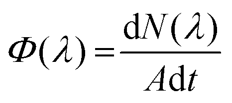
The photon flux Φ(λ) can be estimated by the number of photons [N(λ)] per unit area (A) with time (t), yielding,38,45
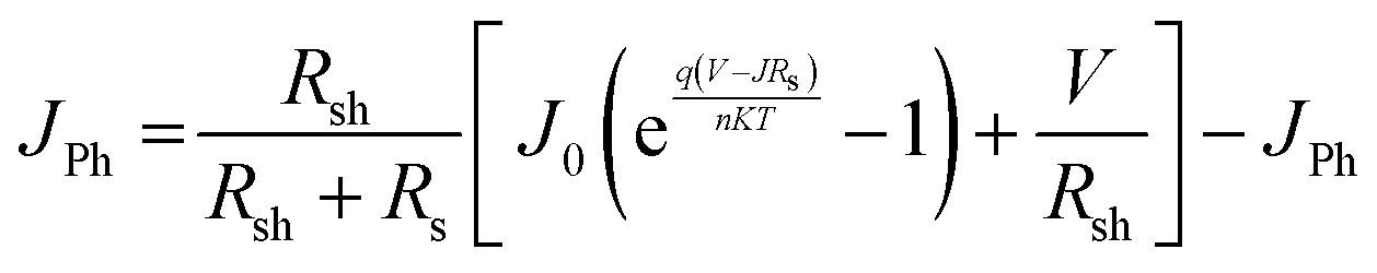
In the open circuit condition, V = VOC, J = 0, then the open circuit voltage (VOC) can be defined as below, assuming Rsh ≫ Rs, the
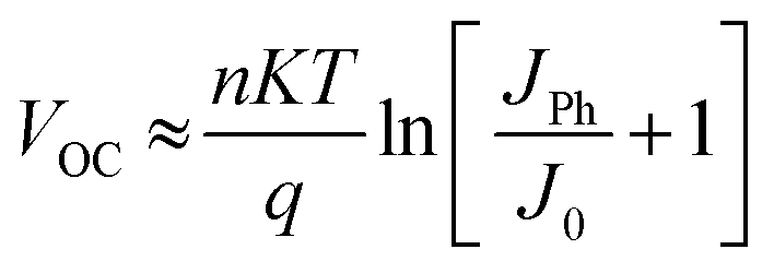 ; where n is a light intensity-dependent factor. If the value of n is close to 1, then there will be fewer chances for recombination. The reduction in JPh value and increase in n value results in an extra loss in energy (Eloss) of 0.15–0.20 eV. This reduction in VOC is mainly because of shifting in the quasi-Fermi levels. The fill factor (FF) is the function of VOC, which increases with the increase in light intensity but this increment possesses a low increase in Rs value.
The energy loss in terms of radiative and non-radiative loss plays a significant role in a sharp decrement in efficiency, especially in low light conditions; this loss for IPVs can be estimated by the following expression:46,47
| Eloss = qΔVradOC,abovetheband gap + qΔVradOC,belowtheband gap + qΔVnon-radOC |
| Eloss = ΔE1 + ΔE2 + ΔE3 |
Fig. 2 is showing the radiative and non-radiative losses, which directly affect the power conversion efficiency (PCE). The PCE of a solar cell is the function of VOC, short circuit current density (JSC), and FF of the device. Usually, the VOC of a solar cell varies VOC ∼ ln(JSC) with the incident light intensity and the JSC of a solar cell varies as power law JSC ∝ Iα. The logarithmic dependence of VOC on light intensity can be explored to determine the diode quality factor ‘n’.49 The diode quality factor n of a solar cell varies usually between 1 and 2. The current in the solar cell is said to be purely diffusive for the value of n = 1 and at this condition, trap-assisted recombination is minimum and band-to-band recombination is maximum.50 A higher diode quality factor between 1 and 2 indicates the dominance of trap-assisted recombination or Shockley–Read–Hall (SRH) recombination.51 The diode quality factor n >2 is observed due to multiple trapping states, indicating the very poor performance of the device.52 Ideally, the power law exponent α should be equal to one, i.e., a linear dependency of JSC on the simultaneous variation of light intensity. The variation in JSC is more rapid than the variation in the VOC value in a solar cell with the variation in light intensity and the effect of shunt resistance on FF under low light conditions being much more stringent.53 The presence of bulk, as well as surface defects inside a solar device, plays a crucial role in solar cell efficiency.54 While bulk defects mainly contribute toward SRH or trap-assisted recombination, excess surface defects deteriorate solar cell performance by hampering the collection carriers. Ryu et al. observed a diminishing of charge carrier trapping due to defects while increasing the intensity of light from 0.01 sun to 1 sun conditions while using MAPbI3-based solar cells.55 The authors have also observed an intensity-dependent diode quality factor, which was correlated with the presence of a separate type of recombination center, depending on the intensity of incident light on solar cells. On a similar device, the FF was observed to first increase monotonically with the light intensity and become saturated at high light intensity. Freunek et al. calculated the detailed balance limit for a fluorescent tube light source for a semiconductor having a bandgap of 1.96 eV and a sodium discharge lamp with a semiconductor having a bandgap of 2.10 eV.12 The upper PCE limits for the fluorescent tube and sodium lamp were observed to be 46% and 67%, respectively. These PCE limits are much higher than the radiative limit proposed by Shockley and Queisser for the AM1.5 spectrum.56 The high indoor efficiency behaviour was observed due to the high charge yield potential for the indoor light sources in comparison to the AM 1.5G spectrum. Narrow-band indoor light emitters are typically designed in the visible spectrum of the light, which helps in enhancing the VOC; also, the high photon-to-charge conversion ratio yields much higher PCE as compared to the STC conditions of a solar cell.
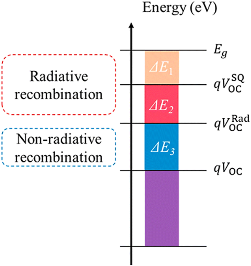 | ||
| Fig. 2 Combination of losses in open circuit voltage from the bandgap energy (Eg) due to radiative and non-radiative recombination. VSQOC is the voltage at the maximum Shockley–Queisser limit and VRadOC is the open circuit voltage under radiative recombination. Reproduced from ref. 48 with permission from [ACS], copyright [2020]. | ||
Parasitic resistance losses due to high series resistance and low shunt resistance contribute significantly toward inferior device performance. As the light intensity in the indoor environment decreases, the ratio of photocurrent and shunt leakage current decreases significantly. This forces the requirement of a much higher shunt resistance of solar cells in the indoor environment conditions as compared to the STC conditions of the solar cell. The minimum shunt resistance (RSH = VOC/JSC) as proposed by Freunek et al. for the silicon device at AM1.5 spectrum is 20 Ohm while for the low light condition, it has to be in the order of a few kilo Ohms.12
3.1 Requirements of the material
As discussed earlier, the irradiance spectrum of indoor light sources comprises only the ultraviolet and visible region photons. Therefore, solar cell materials with narrow absorption bands are required for indoor PV to reduce non-absorption losses and thermalization losses. The spectral content of indoor lighting is limited to the visible region and hence the optimal bandgap for indoor PV is higher than the optimal band gap corresponding to the solar spectrum. The optimal band gap energy for the most efficient performance of the solar cells under indoor lighting is approximately 1.9 eV, whereas the optimal band gap for the outdoor operation of the solar cells is approximately 1.35 eV.12,56,57 Various solar cell technologies based on different absorber materials developed over the years primarily for outdoor applications are Si solar cells, thin film solar cells (GaAs, CdTe, CZTS), dye-sensitized solar cells, organic solar cells, and PSCs. Besides their excellent performances under outdoor conditions, the OPVs, DSSCs, and PSCs are preferred for indoor applications owing to their solution-processability and ease of fabrication. Under low light conditions, the OPVs have already achieved over 31% and PSCs have achieved over 37%.58,59 Considering the scope of the article, we will discuss the development of the PSCs for indoor photovoltaics in detail.For IPVs, the material should satisfy a minimum of certain primary and secondary criteria. The primary criteria are as follows: (1) for achieving high conversion efficiency, the photo response of the active material should match the indoor light spectrum. (2) The material should have minimum VOC loss. (3) The material should have fewer defect states because, under indoor light conditions, trap-assisted recombination plays a significant role, which can impact not only JSC and VOC but can also affect the FF. The secondary criteria are as follows: (1) the material should show less interfacial mismatch or interfacial defects, and needs good Ohmic contact and high charge transfer properties with high optical transparency. (2) To minimize all other losses, such as loss due to thermalization, Eloss, etc., and match indoor light conditions, the band gap (Eg) should correspond to a range of 1.8–2.0 eV. (3) The EQE should be high enough or close to 1. (4) In IPVs, trap-assisted recombination plays a critical role under low-intensity indoor illuminations, thus defects in the active material play a crucial role for IPVs.60,61
Based on the structure, properties and device characteristics, III–V semiconductors, DSSCs, OSCs, and perovskite-based materials are more promising candidates for IPVs. The energy harvesting from indoor light through photovoltaics heavily depends on the purity of the materials and the recombination of electron–hole pairs. Tuneable bandgap semiconductors such as perovskites, DSSCs, and OSCs are generally preferred for the IPV application to ensure better spectral matching with any indoor light sources. Spectral matching is generally explored through the so-called mismatch factor (MMF) with the reference case of STC, i.e., the AM1.5 spectrum. Reich et al. calculated the MMF for various solar cell absorber materials at different light sources.62 Higher spectral matching leads to a higher PCE of the device, regardless of the type of material under consideration. The biggest advantage of IPV devices is that their PCE can be tuned not only by tuning the bandgap of the material but also by tuning the spectral content of indoor light sources as well. Solar insolation is usually measured in the unit W m−2 or mW cm−2. On the other hand, halide perovskites can perfectly cover the UV-Vis to IR range, which is anticipated to be added for the IPVs because of its optoelectronic properties such as low exciton binding energy, high carrier mobility along with being lightweight, flexible, and solution-processable.63–66
4. Overview of non-solution-processed inorganic thin film-based solar cells for the IPV applications
Crystalline silicon-based thin film solar cells have already reached close to their Shockley–Queisser limit under the AM 1.5G spectrum.56 Silicon heterojunction solar cells with interdigitated back contact fabricated by Yoshikawa et al. have proven to have a PCE of 26%.67 Under low light indoor illumination, the PCE limit of low bandgap c-Si was observed to be much smaller than the PCE of wide bandgap absorbers such as a-Si due to spectral mismatch and matching with the indoor light sources, respectively.27 Commercialized silicon-based solar cells have only shown PCE of less than 10% under low light concentrations.68 Inorganic a-Si and Si-based solar cells are highly stable under outdoor as well as indoor operating conditions in comparison to the organic, DSSC, and PSCs.69 Hence, from the stability point of view, these devices have a much longer operational lifetime and therefore, they can be effectively implemented under low light conditions. Amorphous Si-based solar cells have been used since the 1970s in digital watches and calculators.31,61 A small area of 1–10 mm2 silicon-based device fabricated by Moon et al. showed a PCE of magnitude 17% under ultra-low light with an incident power of 660 nW mm−2.70 Such small area devices have also found application in human microchip implants.70 Bunea et al. studied the impact of low light illumination on two different monocrystalline silicon solar cells, one with a low shunt resistance (Rsh < 1000 Ohm cm−2) and the other with a high shunt resistance value (Rsh >1000 Ohm cm−2).71 The device having a high shunt resistance value retained its PCE with a reduction in the light intensity up to two orders of magnitude, while the device having a low shunt resistance value PCE was observed to decrease significantly at the low illumination level. The PCE of the low-resistance device was observed to decrease linearly with a decrease in the illumination light intensity level, while the high shunt resistance device retained its original efficiency. A hydrogenated a-Si: H-based device fabricated by Kim et al. showed an impressive PCE of 36% at a light intensity of 3000 lux and a power density of 0.92 mW cm−2.68 The PCE retained its 99.9% value under continuous exposure to low light illumination for 200 hours. A high-gap triple structure glass substrate/textured fluorine-doped tin oxide (FTO) (600 nm)/p-μc-Si:H (15 nm)/HTMs (a-Si:H; 27 nm)/i-a-Si:H (200 nm)/HTMs (a-Si:H; 27 nm)/n-μc-Si:H (20 nm)/GZO(700 nm)/CAMs [ultrathin silver 8 nm and gallium-doped zinc oxide (GZO); from 50 to 130 nm] ensured a high shunt resistance value for obtaining a high PCE indoor device. Kao et al. studied the effect of i-a-Si:H layer thickness and window layer optimization on the p–i–n device structure of a-Si-based solar cells under indoor as well as outdoor conditions.69 Authors have observed a significant FF degradation under outdoor conditions while increasing the i-layer thickness. However, during the indoor light conditions, authors did not observe a similar FF degradation. Furthermore, the device showed a significant output power (PCE = 24.88% for p-a-SiCCH4=10:H window layer) under indoor light intensity of 500 lux without having any light soaking degradation. The different device behaviours under indoor and outdoor conditions were attributed to less recombination due to defects and dangling bonds inside the indoor light condition.Ruhle et al. studied the superposition of multiple light sources that can be present inside an indoor environment condition.72 The authors have considered the impact of the superposition of indoor light sources such as LEDs and CFLs and outdoor sunlight generally present during the day. They calculated the detailed balance efficiency limit for 4 different light sources, including the standard solar spectrum (AM 1.5G), energy-saving lamp (ESL), halogen bulb, and LED lamp. The spectra of ESL and LED light sources were observed to be optimum for semiconductor materials having bandgaps between 1.5 to 2 eV and also a narrow spectrum range efficiency of solar cells under indoor conditions can reach up to 60%. Freunek et al. determined the ultimate efficiency of a photoconverter and calculated the limit at 46% for a fluorescent lamp at a semiconductor bandgap of 1.95 eV, and 67% for a sodium discharge lamp for a semiconductor bandgap of 2.10 eV.12
Among the flexible IPV devices, a small area (30 cm2) a-Si flexible solar module fabricated by Foti et al. presented a PCE of 9.1% under 100 lux of a fluorescent lamp spectrum and the device was also optimized using the absorber layer interfaces optimization.73
Apart from silicon-based inorganic absorber materials, other absorber materials such as GaAs,57,74–76 CdTe,26,77 CIGS,78 and InGaP79 are also widely studied for IPV applications. Teran et al. studied the GaAs and Al0.2Ga0.8As-based devices (∼ 1 mm2 area under AM 1.5G) with indoor white phosphor LED.57 The Al0.2Ga0.8As-based device demonstrated a PCE of 21% under low lighting conditions. GaAs and Al0.2Ga0.8As cells provided a power density of 100 nW mm−2 at 250 lux, which is sufficient to power the IOT devices. The authors observed stable performances of GaAs and Al0.2Ga0.8As-based solar cells because of low dark current levels and relative insensitivity to shunt current leakage. A combination of high-power conversion efficiency and small low light sensitivity prompted the use of the Al0.2Ga0.8As-based device for the design of small area mm-scale wireless sensor nodes. Kelly et al. studied the GaAs-based solar cells in comparison with DSSC.74 The authors have observed that the power density of GaAs-based solar cells is 3 times higher than that of DSSC. It has been observed that a credit card-sized GaAs solar cell can provide up to 4 mW power to a sensor node kept in dim light conditions (∼200 lux). Teran et al. studied GaAs solar cells for IPV application.76 The GaAs solar cell having a device area of 1 mm2 showed a PCE of 19% at 580 lux. Li et al. compared the performance of GaAs and CdTe solar cells under low light conditions.77 The low series and high shunt resistance of GaAs do not affect the device performance under low-light conditions, whereas low shunt resistance (high series) significantly degrades the CdTe solar cell performance under low-light operating conditions. The authors established an ideal logarithmic function for the variation of PCE in GaAs-based solar cells with the change in irradiation intensity. Yang et al. studied the c-Si and CIGS-based solar cells in indoor light conditions and obtained PCE up to 7.4%.78 Single-junction InGaP-based solar cells fabricated by Dai et al. showed 30% PCE under 1.27 μW cm−2 illumination.79 Authors have optimized the doping density and thickness of absorber layers for effective device design for indoor light conditions. Inorganic thin film solar cells have been studied for a long time and have also been used in indoor applications but they still give much lower efficiency values as compared to other PV technologies. Si solar cells have certain disadvantages as follows: they present poor performances under indoor illumination, they are not cost-effective under low light conditions because the generated power is very low and it incurs greater cost during fabrication as compared to solution-processable technologies, and they are also not compatible for IoT integration due to the limitations posed by the fabrication processes.
Hence, the ease of solution and low-temperature processability to reduce the overall device cost and complexity has forced researchers to develop alternative solar cell absorber materials. In this regard, in the last two decades, researchers have developed solution-processed perovskites, DSSC, organic, and other nanotechnologies-based solar cells as summarized in the following sections.
5. Solution-processed PV Technologies for Indoor Applications
5.1. DSSCs for IPVs
Dye-sensitized solar cells (DSSCs) are a group of solution-processable thin film solar cells that were first introduced by O’Regan and Grätzel in 1991.80 The cell had a light-to-electrical energy conversion yield or PCE of 7.1–7.9% and 12% in simulated solar light and diffuse daylight, respectively. The introduction of a mesoporous semiconductor layer by Grätzel led to a ground-breaking innovation in the DSSC technology. Molecular systems and nanoparticles present in this modern solar cell technology, mimic the process of photosynthesis to convert solar light into useful electrical energy. Simple solution-processable fabrication methods, flexible design, and the use of non-toxic materials allow DSSCs to be implemented in a wide range of applications starting from smart windows, buildings, and offices to consumer electronics and the internet of things (IoT). A schematic representation of the device structure of DSSC is depicted in Fig. 3.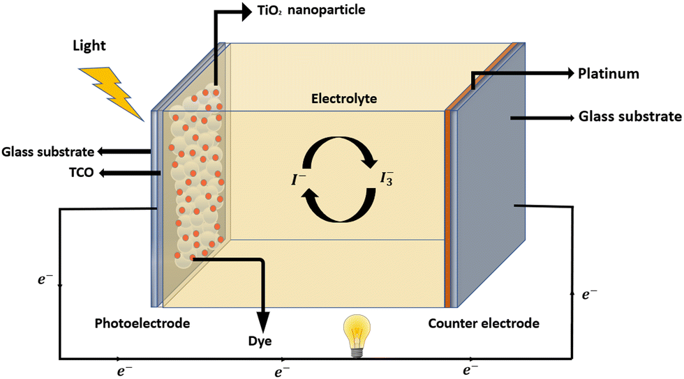 | ||
| Fig. 3 A schematic illustration of a dye-sensitized solar cell. | ||
Under solar light illumination, the dye molecules embedded with the TiO2 surface become excited by absorbing photons and inject photo-generated electrons into the conduction band of the TiO2 layer, leaving the dye in its oxidized state. On diffusing through the TiO2 layer, the electrons finally reach the FTO from where they pass through the external circuit and are subsequently collected by the counter electrode. The dye finally achieves its ground state after receiving electrons from the electrolyte, resulting in the oxidation of I− to I3−. The I3− ions diffuse a short distance through the electrolyte to the counter electrode which acts as the cathode, where it is reduced to I− ions by receiving electrons from the external circuit; thus, the entire cycle is completed. The I3−/I− contained in the electrolyte is called a redox shuttle.81
The chemical structure of dyes greatly affects their performance in terms of efficiency.82,83 Hence, studying the chemical functionalities, their respective positions in the dyes and finally, their overall impact on the DSSCs is an active research area.84 Studies have reported that the optical properties of molecular dyes can be tuned by a small change in the functional group position in a set of isomers.85,86 For example, there are several reports on the impact of alkene functionality on the tunable π-conjugation of a molecular scaffold, including the length of the π-conjugation.87,88 Therefore, the bandgap of DSSCs can be tuned and this property enables the realization of suitable dye absorbers for a variety of applications including indoor photovoltaics. To date, the PCEs of DSSCs have reached beyond 13% under one sun illumination.89 However, under dim indoor light conditions, the PCE has reached over 34%, which demonstrates DSSCs as promising candidates for efficient light harvesting under ambient conditions.90
Optimization of dyes. DSSCs contain a novel dye, also called the sensitizer, which plays a significant role in effective light harvesting.91 On photoexcitation, an electron from the dye is injected into the conduction band of the TiO2 layer and the dye, in turn, accepts an electron from the electrolyte, and thus the cycle repeats itself.92 An efficient sensitizer should have (1) a strong absorption coefficient in the visible range of the solar spectrum; (2) high stability in all three states: oxidized, ground, and excited; (3) appropriate redox potential and (4) efficient charge injection and regeneration processes.93 Ruthenium-based sensitizers, primarily N719, N3, and TF-tBu-C3F7 are very efficient because of their high stability, panchromatic absorption in the visible range, efficient injection of electrons, and charge transfer.94–96 Despite the progress, factors limiting the use of Ru-based dyes are mainly attributed to their time-consuming multi-step preparation procedure, toxicity, and high cost.
Porphyrin is another dye sensitizer that is commonly used in DSSCs. It has a high extinction coefficient, great stability, efficient electron conductivity, and low cost.97 In 2016, Liu et al. reported that DSSCs based on a new porphyrin dye Y1A1 exhibited 19.5% PCE under an indoor LED light intensity of 350 lux.98 Besides being structurally simple, Y1A1 helps molecules to easily dissolve in solvents and avoids the use of hazardous chemicals; hence, it facilitates large-scale fabrication for future industrial purposes. Reddy et al. fabricated SK7, another porphyrin dye that when tested in DSSC, showed remarkable performance in indoor light conditions. The PCE was recorded to be 19.72% in a 6000 lux T5 light source.99 Under the same light conditions, DSSC based on YD2 dye showed a PCE of 20%.100
Anthracene-based molecules have also been implemented in DSSCs since they exhibit unique bright blue electroluminescence properties.101,102 Two anthracene-based dyes were reported to act as co-sensitizers and co-adsorbents to enhance the performance of porphyrin-based DSSCs.103 Wang et al. prepared some cost-effective organic anthracene-based dyes (AN1, AN3, AN5, AN7, AN8) and studied their spectral characteristics, electrochemical properties, and photovoltaic performance.104 Under indoor light conditions (200, 600, and 1000 lux), the AN3-based DSSC module of cell area 0.16 cm2 and flexible panel area of 0 36 cm2, showed a PCE of 5.45%. The long-term stability of AN3-based devices was monitored at room temperature and under indoor light conditions and the overall efficiency was found to drop by only 3% after 2000 hours, which showcased the promising future of AN3 for indoor applications. In 2018, Tsai and his colleagues designed DSSCs based on three novel anthracene-based organic dyes AN-11, AN-12, and AN-14.105 Owing to its strong absorption in the visible range, the DSSC module based on AN-11 dye exhibited a superior photovoltaic performance with an active area of 26.80 cm2 and reached an overall efficiency of 11.95% under indoor luminescence of 1000 lux of T5 fluorescent light. Tingare et al. synthesized metal-free anthracene-based dye having a D–A′–π–A configuration, where D = electron donor, A′ = auxiliary acceptor, π = π-conjugated bridge, and A = electron acceptor/anchor. They revealed that when a similar anthracene-based TY6 dye was used, the indoor DSSCs exhibited a PCE of 28.56% and 20.72% under 6000 lux T5 fluorescent light and LED light, respectively.106 Certain factors like the overlapping of the absorption spectra of TY6 with the blue and red regions of the LED light emission as well as the large energy offset between ELUMO and the conduction band of TiO2, contributed to the excellent performance of TY6-based indoor DSSCs.
Reports of organic dyes for indoor photovoltaics are gradually increasing because of their design flexibility and low fabrication cost due to the vast availability of inexpensive raw materials. Perylene, one kind of structurally tunable polycyclic aromatic hydrocarbon (PAH), has been extensively studied owing to its promising optoelectronic properties, such as strong light absorption in the UV-vis region, chemical stability, and strong fluorescence quantum yield.107,108 Chou et al. designed a series of new dyes having the perylene moiety, termed as G7 series push-pull organic dyes.109 The GJ-BP dye-based DSSC presented a high output power of 0.28 mW cm−2 under 6000 lux light intensity. This is equal to a PCE of 15.79%. Four D–A′–π–A type sensitizers namely MD4, MD5, MD6 and MD7, were developed by Desta et al. for application in DSSCs for indoor purposes as well as in one sun conditions.110 The DSSC based on MD7 dye performed well due to its twisted structure and the presence of alkoxy chains at the donor side. The dye achieved PCEs of 18.95% and 27.17% under indoor light intensities of 300 and 6000 lux irradiance, respectively. Jiang et al. prepared Y-shaped sensitizers by incorporating quinoxaline or quinoxalinoid moieties.111 This enhanced the absorption extinction coefficients and the efficiency of the DSSC in indoor lighting conditions was boosted to 27.76%, 28.74%, and 30.45% under 600, 1000, and 2500 lux irradiance respectively.
Besides employing a single dye, researchers combined two dyes by the co-sensitization technique, which proved to be a very successful way to enhance the PCE, as well as reduce the overall cost of the device, thereby promoting its advantages for powering IoT. Freitag et al. designed two sensitizers coded as D35 and XY1 and combined them with a copper complex as the redox shuttle, thereby obtaining a high PCE of 28.9% under a low fluorescent light intensity of 1000 lux.112 Li et al. prepared YL1-YL4 sensitizers for application in DSSCs.113 YL dyes can efficiently block dark currents owing to their double-layered shelters, the inner shelter arising from the di-anchor skeleton, and the outer shelter from clogged tetraphenylethylene (TPE) units. Under indoor light illumination of a T5 lamp, the YL4-based DSSCs exhibited PCE of 27.54%, 26.81%, and24.98% at 187 lux, 597 lux, and 1025 lux respectively. In 2018, Cao et al. constructed a DSSC with Cu electrolyte and co-sensitizers Y123/XY1b.114 A PCE of 31.8% under 1000 lux of fluorescent light intensity was achieved with a cell area of 2.8 cm2. Tanaka and his co-workers mixed a low cost π–A dye (5T) with a D–A–π–A dye (XY1) and under low light conditions using artificial fluorescence lighting (1000 lux), the XY1 + 5T devices showed a high PCE of 29.2%.115 Recently, Michaels et al. tailored co-sensitized DSSCs by combining a small organic L1 dye with XY1.90 The resultant DSSCs showed an unprecedented PCE of 34% at 1000 lux, 32.7% at 500 lux, and 31.4% at 200 lux of fluorescent lamp irradiation. These DSSCs were capable of powering IoT devices run by machine learning. Zhang et al. were able to achieve the current record efficiency of DSSC in ambient light, 34.5% at 1000 lux, employing an MS5/XY1b co-sensitized photoanode and the [Cu(tmby)2]2+/+ redox couple.89
Optimization of device designs. Apart from employing innovative dyes, new DSSC device designs using alternate redox shuttles and catalyst materials have been incorporated. Since charges are exchanged between the photoelectrode and the counter electrode during cell operation, to avoid a short circuit, the two electrodes are usually encapsulated together with a thick (10–45 mm) spacer foil that is thermoplastic in nature. To prevent short circuits, the electrodes can also be separated by a thick (1–30 mm) and porous insulator (e.g. ZrO2 or Al2O3 based insulating layers).116,117 Cao et al. reported a DSSC employing mesoporous TiO2-based photoanode and a poly(3,4-ethylenedioxythiophene) (i.e., PEDOT)-catalyst-based counter electrode, both in physical contact with each-other having no spacer between them, as depicted in Fig. 4. An impressive PCE of 13.1% under one sun was observed when a liquid electrolyte having a copper (Cu) redox shuttle and TiO2 electrodes co-sensitized with Y123 and XY1b dyes were used.114
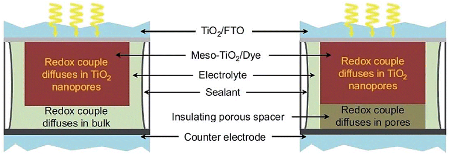 | ||
| Fig. 4 Illustration of DSSC employing either a thermoplastic spacer or an insulating porous spacer. Reproduced from ref. 114 with permission from [CellPress], copyright [2018]. | ||
Although spacer-free DSSCs have achieved high efficiencies, there are certain drawbacks. The increased thickness arising due to the double glass substrate hinders its application for IoT devices. The high cost of the overall device further stands in the way of commercialization. Also, the evaporation process of the solvent for the Cu electrolyte is time-consuming, hence this is an impractical approach for rapid production. Electrical degradation of the PEDOT catalyst is also a drawback. To tackle these challenges, Kokkonen et al. proposed a scalable fabrication technique of advanced monolithic DSSCs by screen-printing or inkjet printing.118 In such device design, active layers are integrated on a single glass substrate and hence, the overall cost is reduced. It also facilitates the lowering of cell resistance by removing the drilled holes and spacer layer or channel produced by an insulator layer or a thermoplastic sealant.
Another important component of the DSSC is the electrolyte containing the ion pair salt, known as the redox shuttle. The conventional iodide/triiodide redox shuttle, as discussed earlier, has been used by many researchers but it has several bottlenecks including its low redox potential and metal corrosion, which hinder the stability of the device. Thus, choosing an appropriate redox shuttle significantly influences the PCE and stability of the device. Lan et al. studied the effects of iodine content in the electrolyte and found that at low intensity, the lower the iodine content, the better the performance of the DSSC.119 The cobalt and copper-based redox shuttle attracted tremendous attention due to their rapid dye regeneration process, voltage attainability greater than 1 V, and high compatibility with alternate catalyst materials.120,121 On tuning the redox potential via ligand engineering, high VOC (>1 V) was achieved by DSSCs employing Co redox shuttles.122 By employing Cu electrolytes, improved PCEs have been demonstrated under ambient light conditions as well as full sun illumination.123 However, this method for manufacturing solid-state DSSCs by introducing Cu-based electrolytes followed by electrolyte solvent evaporation seems impractical because it is not only expensive but also creates additional cell resistance. Printable electrolytes, which can be coated on the photoelectrode using a printing technique, can solve the issues and facilitate the large-scale manufacturing of DSSCs. The photovoltaic parameters of the DSSCs based on different dyes are summarized in Table 1.
| Dyes | E g (eV) | Under indoor illumination | Under solar irradiation | Ref. | ||||||
|---|---|---|---|---|---|---|---|---|---|---|
| Light source | Light intensity (lux) | J SC (μA cm−2) | V OC (V) | FF | PCE (%) | P max (μW cm−2) | PCE (%) | |||
| Y1A1 | 1.84 | FL | 300 | 52.6 | 0.467 | 0.739 | 19.3 | 18.2 | 9.22 | 98 |
| LED | 350 | 56.6 | 0.476 | 0.755 | 19.5 | 20.3 | ||||
| SK7 | 1.91 | FL | 6000 | 739 | 0.584 | 0.778 | 19.7 | 335 | 6.54 | 99 |
| LED | — | 613 | 0.602 | 0.779 | 15.4 | 277 | ||||
| YD2 | 1.89 | FL | — | 721 | 0.582 | 0.783 | 20 | 340 | 11 | 100 |
| LED | — | 626 | 0.604 | 0.785 | 16.5 | 296 | ||||
| AN-3 | 2.29 | T5 | 1000 | 60 | 0.46 | 0.67 | 5.45 | 18.3 | 2.25 ± 0.05 | 104 |
| T8 | — | 60 | 0.43 | 0.63 | 4.85 | 16.4 | ||||
| LED | — | 50 | 0.45 | 0.66 | 4.94 | 15.6 | ||||
| AN-11 | 2 | T5 | 1000 | 61.5 | 1.05 | 0.643 | 11.94 | 41.6 | — | 105 |
| LED | — | 52.9 | 1.04 | 0.647 | 11.26 | 35.6 | ||||
| TY6 | 2.16 | T5 | 6000 | 883 | 0.717 | 0.785 | 28.56 | 506 | 8.08 | 124 |
| — | — | 707 | 0.703 | 0.789 | 20.72 | 394 | ||||
| GJ-BP | 2.03 | T5 | 6000 | 640 | 0.567 | 0.76 | 15.79 | 276 | 6.16 | 109 |
| LED | — | 557 | 0.561 | 0.76 | 13.1 | 237 | ||||
| MD5 | 2.1 | T5 | 6000 | 762 | 0.651 | 0.79 | 23.17 | 394 | 8.39 | 110 |
| MD7 | 2.01 | — | — | 913 | 0.676 | 0.764 | 27.17 | 462 | 9.03 | |
| XY1:D35 | 1.97/2.39 | FL | 1000 | 138 | 0.797 | 0.8 | 28.9 | 88.5 | 7 | 112 |
| MS5/Y1b | 1.72 | FL | 1000 | 138.2 | 0.98 | 0.815 | 34.5 | 109.8 | 13.5 | 89 |
5.2. OSCs and QDSCs for IPVs
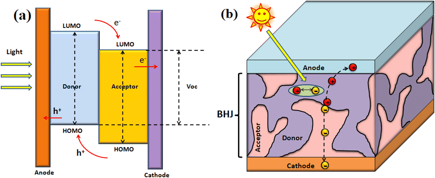 | ||
| Fig. 5 Schematic of the working principle of (a) the two-layer donor–acceptor heterojunction, (b) a bulk heterojunction-based organic solar cell. | ||
Under indoor low light conditions, photovoltaic cells show a very different performance from that in outdoor conditions. Nowadays, the OPV system is receiving great research attention under indoor artificial lighting conditions due to its unique advantages over other photovoltaic technology. It was found that compared to silicon, OPV and DSSCs show better performance under indoor lighting conditions due to the tunable optical properties of their photoactive layer.112 In contrast to Si, the tuning of the optical properties by altering their molecular components helps with obtaining suitable wide bandgap materials for indoor photovoltaics in the cases of OPV and DSSCs. Furthermore, organic photovoltaics possess a greater possibility for commercial application due to their solution-processed cost-effective large-area fabrication routes including doctor blading, other printing technologies, etc. For example, Mori et. al investigated and compared the performances of OPV and crystalline silicon-based PV cells under LED irradiation and obtained a PCE of 21.3% for organic cells.132 To achieve high photocurrent under indoor low light conditions, maximum light absorption should be ensured. This can be obtained by increasing the photoactive absorber layer thickness. In OPV, the thickness is limited to the charge carrier diffusion length because of lower charge carrier mobilities in organic semiconducting materials in contrast to the inorganic counterparts.133 However, their strong absorption coefficients (typically >105 cm−1) and tunable absorption range allow the effective absorption of light, thus making them suitable for thin film applications. In photovoltaic devices, to achieve maximum photocurrent the bandgap of photoactive material should match the emission spectra of the incoming light.48 The absorption coefficients of the organic materials are highly tunable and unlike their inorganic counterparts, the energy levels of the donor and acceptor layers in OPV can be easily adjusted using various molecular design approaches, thus making the band gap appropriate for matching the emission spectra of the incoming light. Adjusting the energy levels of the active layer enables the development of suitable wide bandgap materials for indoor applications. Shim et al. demonstrated a wide bandgap material, PDTBTBz-2Fanti:PC71BM and a crystalline silicon photovoltaic under 500 lux LED illumination and obtained a PCE of 23.1% for the PDTBTBz-2Fanti:PC71BM-based device and 16.3% for the crystalline silicon photovoltaic.134 Moreover, when a more electronegative element substitutes one or more atoms in the extended π-network of organic semiconductor material, the energy level of both LUMO and HOMO can be lowered. Coupling non-fullerene-based low bandgap acceptor material with polymer-based wide bandgap donor material can also extend the absorption spectrum and thus improve the short circuit current density (JSC) and power conversion efficiency (PCE) of the device. Yan et al. utilised M6 as an acceptor and Y6-O as donor polymer materials with PDI-NO as an electron extraction layer. They obtained a PCE 31% under LED light with 100–1700 lux power. This increased PCE has been attributed to the lower HOMO level and excellent hole-blocking ability of PDI-NO, thus minimizing the recombination losses and leakage current in the device.58 Organic photovoltaics with ternary blends (donor:donor:acceptor (D1:D1:A) and donor:acceptor:acceptor (D:A1:A2)) also improved the light-harvesting abilities of the device.135 The addition of a third component provided an additional charge transport path in the ternary blend active layer, thus improving the short circuit current density (JSC), open circuit voltage (VOC) and fill factor (FF) of the device.
Significant efforts have been made by researchers to develop semiconducting organic materials for indoor organic photovoltaic (IOPV) systems. Mainville et al. reviewed various donor and acceptor materials used for IOPV systems.136 Fullerene and its derivatives, such as phenyl-C61-butyric-acid-methyl ester (PC61BM), and [6,6]-phenyl C71-butyric acid methyl ester (PC71BM), indene-C60 bisadduct (ICBA), are the most used acceptor materials in IOPVs.125 PC61BM and PC71BM are more common because they can be easily synthesized via solution-processing using common solvents, while IO-4Cl, IT-4F, ITCC, ITIC-M, and ITIC-F, etc., are some of the non-fullerene based organic semiconducting polymers used as acceptor materials. Saeed et al. analyzed the performance of PC70BM (fullerene-based acceptor) and modified the ITIC-based non-fullerene acceptor (3,9-bis(2-methylene-(3-(1,1-dicyanomethylene)-indanone))-5,5,11,11-tetrakis (4-hexylmeta-phenyl)-dithieno [2,3-2′,3′-d′]-s indaceno [1,2b:5,6b] dithiopheneethylexyloxy) (m-ITIC-O-EH)) with an alkoxy side chain under indoor (LED and halogen lamp) and 1-sun conditions.137 They observed that m-ITIC-O-EH-based devices showed greater efficiencies than fullerene-based acceptor devices under all three illumination conditions. Several organic polymers and small molecules (like P3HT, PCDTBT, PPDT2FBT, and BTR, etc.) having semiconducting properties, are used as donor materials in OSCs for indoor application. The difference between the working mechanisms of outdoor and indoor organic photovoltaic and material requirements for IOPV have been well explained by Cui and co-workers in their article.48 They also summarized the performance of various donor–acceptor materials developed for IOPV under different illumination conditions. Material for IOPVs slightly differs from that used for OSCs. It has been reported that the absorption spectrum of semiconducting polymer-based OPVs matches the irradiance spectrum of indoor light sources such as white LEDs or fluorescent lamps.61 Therefore, OPVs show better PCE under indoor lighting conditions than under sunlight; they also show better responses under variable incident light angles, making them suitable for fabrication over flexible and lightweight plastic substrates.138 Such vast advantages allow them to be installed on curved surfaces, thus making them ideal for harvesting light for low-power-consuming portable indoor electronic devices for future IoTs.125 In addition, under indoor application, OPV shows better stability as compared to outdoor application because the photooxidation of OPV does not occur in the indoor environment.139 Furthermore, it has been reported that IOPVs require high shunt resistance while series resistance has less impact on the device performance.140–142 Shunt resistance affects the VOC and photocurrent of the device. Under low lighting conditions, less current is generated so high shunt resistance is important to achieve fewer recombination losses. On the contrary, series resistance does not show a severe impact on device performance under low light conditions. To get the desired response from IOPV, a device must have low optical losses due to the low intensity of indoor light. To achieve low series resistance and high transmittance, Kim and co-workers utilized very thin ITO film doped with Ni in a poly(3-hexylthiophene):indene-C60-based active layer.143 Shin et al. made use of poly[(2,5-bis(2-hexyldecyloxy)phenylene)-alt-(5,6-difluoro-4,7-di(thiophen-2-yl)benzo[c][1,2,5]thiadiazole)](PPDT2FBT) and a fullerene derivative, PC70BM, as a photoactive layer.144 They observed a lower series-to-shunt resistance ratio even at a higher thickness of the active layer, thus concluding that the short circuit current and FF of the device are less impacted by the thickness of the device. Lechêne et al. suggested that instead of shunt resistance, the ratio of dark current to short circuit current densities can be a reliable criterion for understanding the OPV under low light.145 The value of shunt resistance is different for different systems and it depends on the ratio of dark current to the short circuit density of the device. Thus, minimizing the dark current of the device is necessary to improve the PCE in an indoor environment. Since OPV under low light intensity under indoor conditions is independent of series resistance and active layer thickness, it is suitable for fabricating large-area devices.
In IOPV, obtaining high VOC is important for achieving higher photovoltaic performance. Carrier density in OPV is proportional to the light intensity; OPV devices show reduced VOC under low light conditions but higher FF is obtained due to low bimolecular recombination caused by fewer photogenerated carriers under low illumination. However, trap-assisted recombination comes into the picture under low light conditions. Chen et al. investigated the effects of traps on the organic photovoltaic utilizing PBBD-T, PBDB-TF, and PBFB-TCl as the donor and BTA3 as a non-fullerene acceptor material for all three devices using LED as a light source.146 They explained that shallow-level traps exist in OPV due to the discrete density of states. A lower carrier density under low lighting conditions results in trap assisted-recombination, which impedes the performance of IOPVs. A reduction in VOC has been seen for some polymer-based OPVs under low light intensity. Arai et al. evaluated the indoor photovoltaic performance of solution-processed inverted OPV with device structure ITO/ZnO/BHJ active layer/MoO3/Ag.147 Here, the BHJ active layer consists of small molecules, BDT-2TID and BDT-1T-ID denoted as BDT-nT-ID as the donor and fullerene-based PNP (N-phenyl-2-phenyl[60]fulleropyrrolidine) as the acceptor. BDT-2TID and BDT-1T-ID possess band gaps (Eg) between 1.7–1.8 eV and large absorption coefficients. The absorption spectra matched with the emission spectra of white LED so it is considered a promising material for indoor energy-harvesters. The author used white LED light as an illumination source (200 to 10000 lux (lm m−2)) and was able to obtain a PCE of 16.2% at 200 lux illumination intensity. They observed that JSC was directly related to the incident light intensity, which suggests a suppressed bimolecular recombination. However, a decrease in VOC was observed as the light intensity decreased. Various approaches have been employed to enhance the VOC of the IOPV system. Some of them include minimizing recombination losses by tuning the polymer's chemical structure, the increment of the energy of charge transfer states, etc. Solvent vapour annealing (SVA) of the active layer during the synthesis process as an additional step has been reported to achieve high PCE.148 The device shows the highest efficiency value of 26.2% (200 lux) and 28.1% (1000 lux) under optimized SVA time. Singh et al. used benzodithiophene (BDT) as an electron donor and 5,8-bis(5-bromothiophen-2-yl)-6,7-difluoro-2,3-bis(3-(octyloxy)phenyl)quinoxaline as a function of the BDT's thienyl substitution (alkyl (WF3), alkylthio (WF3S) and fluoro (WF3F)).149 PC71BM was used as an acceptor and diphenyl ether (DPE) was used as an additive during the synthesis process. Reduced bimolecular recombination and series resistance and an increment shunt resistance were observed on the WF3F:[6,6]-(PC71BM)-based device. Also, they concluded that high shunt resistance does not lead to high VOC but higher VOC is critical for higher PCE and reduced series resistance is essential to achieving high JSC. Lee et al. studied the performance of three different donor materials, such as poly(3-hexylthiophene-2,5-diyl) (P3HT), poly[N-90-heptadecanyl-2,7-carbazole-alt-5,5-(40,70-di-2-thienyl-20,10,30-benzothiadiazole)] (PCDTBT), and poly[[4,8-bis[(2-ethylhexyl)oxy]-benzo[1,2-b:4,5-b0]dithiophene-2,6-diyl][3-fluoro-2-[(2-ethylhexyl)carbonyl]thieno[3,4-b]thiophenediyl] (PTB7), used in OPV under low light illumination.150 They found that PCDTBT-based devices show higher power output under indoor conditions. The bandgap of PCDTBT (1.9 eV) matches the emission spectrum of fluorescent lamps or visible LED light. The PCDTBT-based device shows high VOC under one sun; also, due to its low ideality factor it demonstrated high device performance under low light. Researchers have also developed a ternary as well as quaternary BHJ photoactive layer to enhance the performance of IOPV. For example, Yin et al. demonstrated ternary BHJ cell PCDTBT:PDTSTPD:PC71BM. It showed enhanced performance compared to the binary BHJ cell of PCDTBT:PC71BM.151 By SVA treatment the device is capable of showing 20.8% PCE under 300 lux of illuminance. However, the binary PCDTBT:PC71BM-based device has less hole mobility. An enhancement in performance in the ternary BHJ device is attributed to the improved hole mobilities, which impact the FF. Also, PDTSTPD can passivate the shallow trap states near the band edge of the BHJ layer showing a sharpened absorption band edge. Similarly, Singh et al. introduced non fullerene EP-PDI as an acceptor to PTB7: PC71BM thus forming a ternary blend of PTB7: PC71BM:EP-PDI.152 Introducing EP-PDI has resulted in the enhancement of photon absorption, better charge transport, and suppressed bimolecular recombination. Also, it has been reported that quaternary IOPVs show better response and stability as compared to ternary counterparts.153 By utilizing a small molecule named IO-4Cl as an acceptor having an optical bandgap of 1.80 eV and by blending with a polymer donor material named PBDB-TF to form an acceptor–donor–acceptor (A–D–A) structure, a very low voltage loss less than 0.60 eV was achieved.154 Ding et al. demonstrated an all polymer-based donor–acceptor blend (CD1:PBN-10) and compared the result with the CD1:ITIC-based device under different light illumination conditions.155 Compared to CD1:ITIC, the device based on CD1:PBN-10 showed higher JSC and VOC under LED and FL illumination, which finally contributed to higher PCE. Moreover, the CD1:PBN-10-based device showed the highest PCE using a fluorescent lamp under 2000 lux illumination intensity. This is attributed to the well-matched EQE spectra with the illumination spectra of LED and FL. Nam et al. studied a ternary organic blend based on a two donor-one acceptor (2D:1A) device and one donor-two acceptor (1D:2A) device utilized for OPV under indoor and outdoor conditions.156 The 1D:2A-based device presented better PCE and less charge recombination irrespective of varying illumination conditions, while the performance of the 2D:1A-based device depended on the irradiation conditions and emission spectra of the light source (Fig. 6).
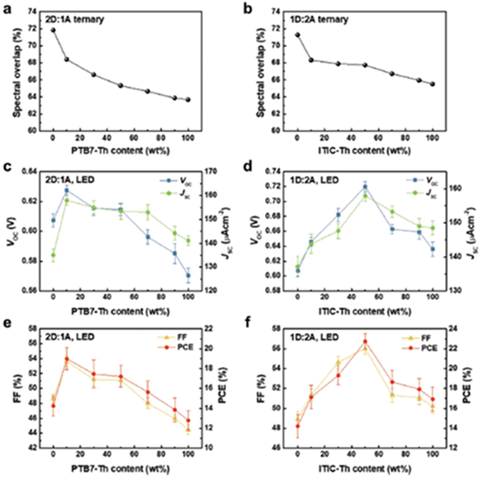 | ||
| Fig. 6 Spectral overlap between the emission spectrum of an LED and absorption spectrum of ternary blends with varying amounts of (a) PTB7-Th in 2D:1A and (b) ITIC-Th in 1D:2A ternary systems. (c and d) VOC and JSC of 2D:1A and 1D:2A ternary OPVs with different amounts of PTB7 and ITIC-Th, respectively (e and f) FF and PCE of 2D:1A and 1D:2A ternary OPVs with different amounts of PTB7 and ITIC-Th respectively. Reproduced from ref. 156 with permission from [Wiley], copyright [2019]. | ||
So far, the organic photovoltaic has attained a power conversion efficiency of over 31% under an LED lamp with intensity ranging from (100–1700) lux.58 Proper optimization of process parameters and methods to effectively collect incident low light and reduction of trap-assisted recombination may further boost the performance of IOPV. One of the major issues hindering the PCE of IOPV is the narrow emission spectrum of indoor light. Due to low light intensity under indoor illumination, OPV showed low photocurrent and extra voltage loss, which contributed to the lower open circuit voltage. To absorb more incident photons, the donor material should be of a lower bandgap to obtain a high JSC value.
In contrast, for higher VOC, the donor material should be of a wide bandgap. Therefore, for improving the PCE of the device, the donor bandgap should be of optimum value. For a multicomponent bulk heterojunction configuration, for example, quaternary BHJs are promising and have shown enhanced charge transport with low recombination loss under indoor light.157 Moreover, non-fullerene-based acceptor materials with bandgaps greater than 1.8 eV in the donor–acceptor BHJ configuration compete with other photovoltaic technologies for indoor applications. The application of metal nanoparticles in the active layer has been shown to increase the efficiency of OPV both under AM 1.5G and under indoor applications.158 Metallic nanoparticles contribute to the localized surface plasmon resonance phenomenon, which enhances the scattering and accumulation of incident light within the active area, resulting in a highly efficient device. The performances of organic solar cells under indoor illuminations for different active layers have been summarized in Table 2.
| Sl. no. | Active layer | Bandgap (eV) | Under indoor illumination | Under solar irradiation | Ref. | ||||||
|---|---|---|---|---|---|---|---|---|---|---|---|
| Light source | Light intensity (lux) | Jsc (μA cm−2) | V OC (V) | FF (%) | P max (mW cm−2) | PCE (%) | PCE (%) | ||||
| 1 | WF3F:PC71BM | 1.78:1.9 |
LED | 500 | 63.57 | 0.69 | 67.39 | 0.17 | 17.34 | 9.44 | 149 |
| 2 | PPDT2FBT:PC70BM | 1.76:1.7 |
LED | 1000 | 117 | 0.587 | 65.2 | 0.0448 | 16± 0.5 | 7.3 ± 0.4 | 144 |
| 3 | P3HT:ICBA | 2.18:1.7 |
FL | 500 | 50 | 0.73 | 62.0 | 0.02257 | 13.76 | 4.90 | 159 |
| LED | 500 | 50 | 0.73 | 63 | 0.02297 | 13.05 | |||||
| P3HT:P60CBM | 2.18:2 |
FL | 500 | 62 | 0.43 | 59 | 0.01577 | 9.5 | 3.68 | ||
| LED | 500 | 62 | 0.43 | 59 | 0.01567 | 8.90 | |||||
| PBDTTT-EFT:PC70BM | 1.6:1.96 |
FL | 500 | 63 | 0.58 | 59 | 0.02156 | 13.14 | 6.95 | ||
| LED | 500 | 66 | 0.59 | 58 | 0.02323 | 13.20 | |||||
| 4 | PCDTBT:PC71BM | — | FL | 300 | 30.7 | 0.70 | 56.4 | 0.0122 | 16.5 | 5.3 | 151 |
| PCDTBT:PDTSTPD:PC71BM | FL | 300 | 33.3 | 0.73 | 63.5 | 0.0154 | 20.8 | 6 | |||
| 5 | P3HT:PC60BM | 2.18:2 |
FL | 300 | 20.6 | 0.41 | 56.6 | 0.0048 | 5.8 | 2.4 | 150 |
| PCDTBT:PC71BM | 1.9:1.9 |
FL | 300 | 27.7 | 0.72 | 69.3 | 0.0139 | 16.6 | 6.0 | ||
| PTB7:PC71BM | 1.8:1.9 |
FL | 300 | 28.6 | 0.61 | 69.5 | 0.0122 | 14.6 | 6.8 | ||
| 6 | PTB7:PC71BM:EP-PDI | 1.84:1.9:2.3 |
LED | 500 | 57.8 | 0.65 | 68.5 | 15.68 | 8.53 | 152 | |
| 7 | CD1:PBN-10 | 2.37:2.39 |
FL | 1000 | 120 | 1.14 | 66.2 | 0.091 | 26.2 | 7.93 | 155 |
| LED | 1000 | 105 | 1.14 | 65.4 | 0.078 | 21.7 | |||||
| CD1:ITIC | 2.37:1.65 |
FL | 1000 | 116 | 0.78 | 68.1 | 0.062 | 17.9 | 8.69 | ||
| LED | 1000 | 107 | 0.77 | 67.5 | 0.056 | 15.4 | |||||
| 8 | PBDB-T:ITICTh:PC71BM | 2.05:1.73:1.98 |
LED | 1000 | 157 | 0.72 | 65.1 | 0.074 | 26.4 | Approx 9.4 | 156 |
| 9 | P3HT:ICBA | 1.7:2.3 |
LED | 1000 | 104.7 | 0.56 | 60 | 0.035 | 14.6 | 0.3 | 143 |
| 10 | PBDB-TF:IO-4CL | 1.8:1.89 |
LED | 200 | 18.2 | 1.03 | 71.5 | 13.4 | 22.2 | 9.8 | 154 |
| 500 | 45.1 | 1.07 | 76.8 | 37.1 | 24.6 | ||||||
| 1000 | 90.6 | 1.10 | 79.1 | 0.079 | 26.1 | ||||||
| 11 | PM6:TB-4F | 1.8:1.71 |
LED | 1000 | 119 | 0.693 | 77.89 | 64.23 | 21.05 (20.4 ± 0.43) | 15.24 (14.99 ± 0.203) | 160 |
| 12 | PBDB-TS:IT-4F | 1.81:1.52 |
FL | 500 | 66.8 | 0.36 | 30.9 | 0.0075 | 5.3 | 8.7 | 161 |
| 1000 | 125.5 | 0.48 | 36.2 | 0.022 | 7 | ||||||
| PBDB-TS-3Cl:IT-4F | 1.82:1.52 |
FL | 500 | 62.8 | 0.64 | 72.2 | 0.0292 | 20.4 | 12.6 | ||
| 1000 | 123.8 | 0.66 | 72.8 | 0.0602 | 19.4 | ||||||
| PBDB-TS-4Cl:IT-4F | 1.82:1.52 |
FL | 500 | 64.9 | 0.64 | 73.9 | 0.031 | 21.7 | 12.7 | ||
| 1000 | 129.3 | 0.66 | 74.3 | 0.064 | 20.7 | ||||||
Otsuka et al. fabricated silicon nanocrystal (SiNC)-based hybrid solar cells on demonstrating indoor light harvesting applications. SiNCs are blended with p-type semiconducting polymer PTB7 or PTB7-Th to create a bulk-heterojunction-type photoactive layer (Fig. 7).166 The fabricated device (ITO/PEDOT:PSS/(SiNCs + PTB7-Th)/Al) showed an efficiency of 3.1% under 1 sun illumination. The same type of device under indoor light at 1000 lux showed 9.71% PCE, promising to power low-power IoT devices.
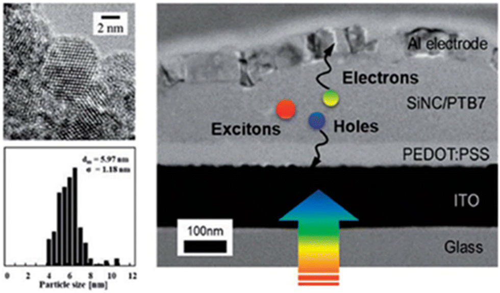 | ||
| Fig. 7 Cross-section Transmission Electron Microscopy (TEM) micrograph of the SiNC-hybrid photovoltaic device. The inset shows the TEM micrograph of SiNCs and their size distribution. Reproduced from. ref. 166 with permission from [RSC], copyright [2020]. | ||
Hou et al. fabricated PbS quantum dot-based solar cells, which showed good performance in indoor light. Multi-photon absorption (MPA) enables PbS QDs to harvest the energy of photons over a wide variety of light conditions (Fig. 8a).167 Interestingly, PbS QDs with tetrabutylammonium iodide (TBAI) ligand showed suppressed Auger recombination, resulting in a linear response of the active layer with an increase in light intensity. The PbS QD-based solar cells performed excellently under varying indoor light (fluorescent lamps) intensity (Fig. 8b), achieving 19.5% PCE at 2000 lux. In addition, the devices showed outstanding stability for 1800 h. of continuous 1000 lux light exposure (Fig. 8c). The high PCE and stability prove the potential of QDSCs for indoor light harvesting applications.
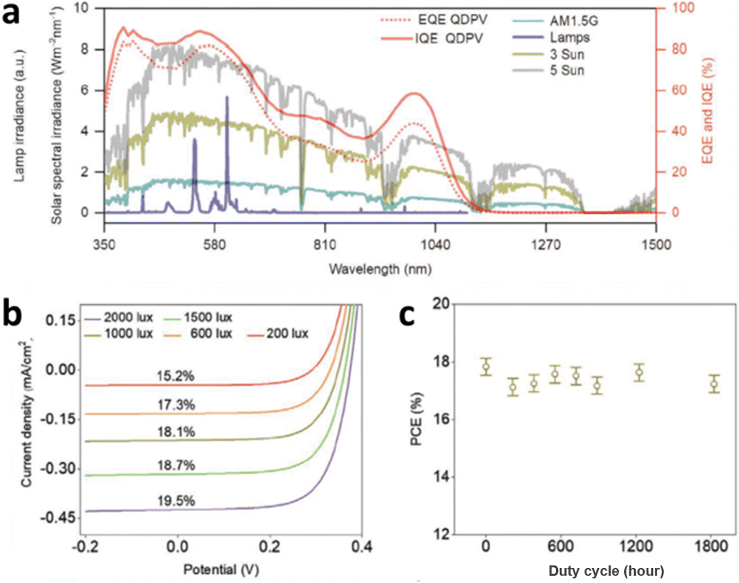 | ||
| Fig. 8 (a) The spectra for AM 1.5G and low-concentration (e.g., 3 and 5 suns) solar irradiance, a fluorescent lamp (1000 lux), and the QE (external and internal) spectra derived from 1.24 eV PbS QDs. (b) J–V curves and PCE values at different room light irradiance levels. (c) The unencapsulated QDSC PCE stability performance under 1000 lux insolation for a continuous 1800 h of exposure. Reproduced from ref. 167 with permission from [Wiley], copyright [2020]. | ||
5.3. PSC for IPVs
In the last few years, PSCs have developed very rapidly and have been established as potential PV technology. The efficiency of PSCs ramped up very fast, up to 25.5% from 3.8%, since being first reported in 2009.168,169 Perovskites generally follow the ABX3 cubic structural framework, where the A cation (organic/inorganic) is positioned at the corners of the cube, the B cation (metal) is body-centered, and X represents halide ions in the face-centered cubic arrangement, as shown in Fig. 9.170 Metal halide perovskites have a broad absorption range, long charge carrier diffusion length, high extinction coefficient, and high carrier mobility, qualifying them as excellent light absorber materials for solar cells.171–175 Also, the perovskite materials possess unique defect tolerance capability, tunable bandgap, and are solution-processable at low temperatures.176,177 In recent years, PSCs have also emerged as worthy contenders for indoor photovoltaics. The low-temperature solution-processability of the perovskite materials allows them to easily produce flexible indoor PSCs and these flexible PV devices can be suitably integrated as power sources for other gadgets.13,178 By varying the contents of halogens, organic ions, and metals, the bandgap of the perovskites can be tuned easily over a wide range and can be optimized for different applications. The optimal bandgap of the absorber materials for the most efficient absorption in an indoor environment, as suggested by the theoretical calculations, is approximately 1.9 eV.12 Bandgap tunability by compositional changes allows for better matching with the indoor light spectrum, which results in increased output power by maximization of the current and voltage. Therefore, by efficient bandgap engineering, it is possible to achieve high-performing PSCs in indoor or dim light conditions. Despite the immense potential of PSCs, their environmental stability is still the major hindrance to the commercialization of PSCs and continuous efforts are being made to address this issue. In an indoor environment, the devices are less affected by harsh weather variations than in an outdoor environment. In addition, the PV-integrated device (e.g., IoT device) lifetime is much lower than the commercial PV panel, which gives PSCs an extra edge to be used ubiquitously in indoor applications. The use of toxic lead as a major component for the absorber of high-performing PSCs raises concerns about using perovskite materials in indoor environments.179 Significant research is going on to realize lead-free perovskite absorber materials for high-performing PSCs with enhanced stability.180,181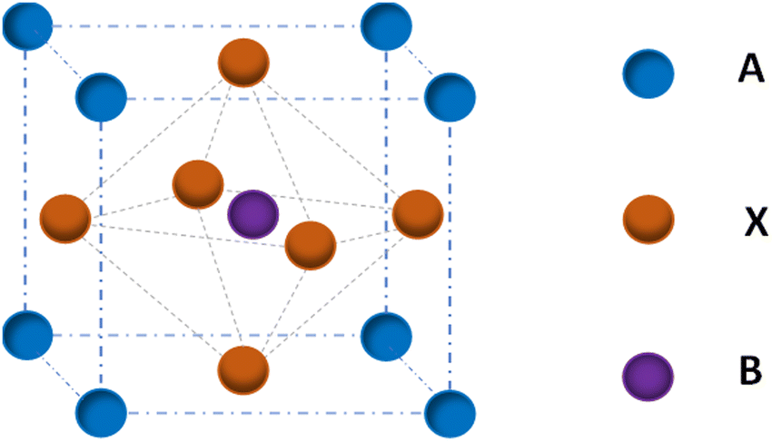 | ||
| Fig. 9 The perovskite crystal structure having a general formula of ABX3. | ||
Perovskite solar cells have presented high PCEs tested under 1 sun illumination in many reports.49,182–184 However, to date, there are relatively fewer studies available on the performance of PSCs in indoor environments but it is evident from the available literature that PSCs also perform quite well under indoor or dim-light conditions. In 2015, Chen et al. studied CH3NH3PbI3−xClx-based PSCs at 100–1000 lux illumination from a fluorescent lamp of color temperature 6500 K and achieved 22.5–27.4% PCE for small area devices.185 Also, a large area device with a device area of 5.44 cm2 presented a good PCE of 20.4% under 1000 lux illumination and could generate 340 μW of steady power which is capable of powering the sensing nodes of IoT. The structure of the fabricated inverted PSC was ITO/PEDOT:PSS/perovskite/PC61BM/1,3,5-tri(m-pyrid-3-ylphenyl)benzene(TmPyPB)/Ag. A two-step deposition process was adopted to deposit PC61BM ETL, which successfully passivated the defects between the perovskite and PC61BM interface. Fewer photocarriers are generated in dim-light illumination rather than bright-light illumination and hence the reduction of traps via interface modification plays a crucial role under dim-light conditions. As a result of defect passivation at the interface, the device exhibited high efficiency with negligible hysteresis under indoor light conditions. In 2016, Raifuku et al. investigated the characteristics of PSCs under low illumination for indoor applications.186 After performing impedance spectroscopy, they observed better performance in planar-type solar cells than mesostructured solar cells under low-illuminance conditions. The mesoporous TiO2 ETL, with fewer photogenerated carriers increased the internal resistance of mesostructured PSCs under low-intensity illumination. As a result, the electron collection efficiency decreased and so the VOC had decreased in the case of mesoporous TiO2 ETL-based devices. Similarly, Ann et al. found that compact-TiO2-based PSCs produced more power than the mesoporous-TiO2-based PSCs under low light conditions (200–1600 lux), while the mesoporous-TiO2-based devices generated higher power under standard 1 sun conditions.187 Although the mesoporous-TiO2 benefits from its morphology, it was non-beneficial for charge collection at the interface in low light conditions. The carrier recombination probability was higher with a greater surface area of mesoporous TiO2 containing more interface defects and deep-level defects. A higher interfacial trap density was the major factor behind the significant power loss of mesoporous TiO2-based devices and this factor proved to have a significant role in the performance of the PSCs under weak light conditions. Furthermore, by applying organic ETL PCBM in a similar device design, they achieved high maximum power densities of 23.61, 39.13, 73.69, and 151.27 μW cm−2 under 200, 400, 800, and 1600 lux LED illumination and maximum power densities of 56.43, 100.97, 187.67, and 376.85 μW cm−2 under 200, 400, 800, and 1600 lux halogen illumination.
Giacomo et al. studied the performance of mesoscopic PSCs utilizing both low-temperature processed compact and mesoporous TiO2 layers under 1 sun conditions and also under low illumination conditions.188 At first, the TiO2 compact layers were fabricated by three different deposition routes: high-temperature spray pyrolysis, high-temperature sol–gel processing, and low-temperature atomic layer deposition. The authors also demonstrated the application of low-temperature atomic layer deposited compact layers to prepare flexible PSCs based on plastic substrates. The low-temperature atomic layer deposition yielded high-quality, pinhole-free compact layers, which enabled highly efficient mesoporous perovskite solar cells under both 1 sun and an indoor environment. The devices presented an excellent PCE of 15.9% under 1 sun condition along with outstanding performance under indoor CFL illumination. A PCE of 24% with MPD of 15.4 μW cm−2 and PCE of 25.4% with MPD of 32.6 μW cm−2 were achieved under 200 and 400 lux illumination levels, respectively. This study suggests that for indoor operations of PSCs, very low reverse dark currents are extremely important for increasing the short circuit current as there are fewer photogenerated carriers. Also, PSCs fabricated on flexible substrates are lightweight, bendable, and can be easily integrated into a range of IoT devices. Lucarelli et al. fabricated flexible PSCs and demonstrated their performance under white LED light sources of illumination of 200 and 400 lux.189 The device was prepared on PET/ITO substrate and used CH3NH3PbI3−xClx as a semiconducting layer and spiro-MeOTAD as HTL. Out of two configurations, using only a compact TiO2 layer, and using a compact TiO2 layer with TiO2 mesoporous scaffold, studied under STC 200 and 400 lux LED illuminance, the device with the mesoporous scaffold presented better performance. The mesoscopic devices achieved high efficiencies of 10.8%, 12.1%, and 9.2% at 200 lux, 400 lux, and STC, respectively. The devices also presented impressive maximum power densities of 7.2 μW cm−2 at 200 lux and 16.0 μW cm−2 at 400 lux. However, the flexible PSCs presented lower efficiencies than their rigid counterparts but they performed better than commercial a-Si rigid modules and flexible DSSCs under LED illuminance. In 2018, Dagar et al. applied a solution-processed SnO2/MgO composite as the electron transport layer in CH3NH3PbI3-based planar PSCs that obtained impressive power outputs in indoor illumination conditions.190 Under white LED lamp illumination, they achieved maximum power densities of 20.2 μW cm−2 and 41.6 μW cm−2, and PCE of 25.0% and 26.9%, at 200 lux and 400 lux, respectively. Insertion of the MgO interfacial layer caused more uniform films and reduced interfacial recombination, hence these values are ∼20% higher than the solar cells with SnO2 only. Noh et al. utilized a bilayer structure of SnO2/ZnO as the ETL in MAPbI3-based planar heterojunction PSCs.59 Due to the inclusion of ZnO between ITO and SnO, well-matched energy levels were ensured and trap-assisted recombination at the perovskite interfaces was suppressed. By virtue of the bilayer ETL, the optimized device with non-annealed ZnO resulted in a record high PCE of 37.2% with a high VOC of 0.98 V under 1000 lux white LED (6500 K) illumination. The devices also presented impressive ambient stability with a stabilized power density of >97.5 μW cm−2 for 800 h under continuous LED illumination (1000 lux).
Better charge transport layers result in better movement of the photogenerated charge carriers. Besides the developments in the ETL materials, researchers have also tried to develop suitable HTL materials to enhance the performance of PSCs under low light conditions. Jagadamma et al. applied low-temperature solution-processed NiO thin films as HTL in p–i–n-type PSCs and showed that NiO thin films resulted in better-performing PSCs as compared to PEDOT:PSS.53 In addition to the improved stability of the device, the excellent hole extraction capability and low recombination rate of NiO resulted in high PCE of the device under indoor or low light illumination. Mixed halide perovskites are optimized in this study as they have larger bandgaps, which is beneficial for indoor light harvesting. They provide better spectral overlap for the device EQE spectra with the spectra of the indoor light sources (fluorescent lamp and white LED light). Under white LED illumination (2.2 mW cm−2), CH3NH3PbI2.9Br0.1 and CH3NH3PbI2.9Cl0.1 mixed halide perovskite solar cells presented high PCEs of 19.9% and 20.8%, whereas the CH3NH3PbI3-based devices presented 14.1% efficiency. The mixed halide PSCs also performed well under fluorescent lamp illumination (0.32 mW cm−2) as CH3NH3PbI2.9Br0.1 and CH3NH3PbI2.9Cl0.1-based devices achieved PCEs of 20.4% and 23.0%, whereas the CH3NH3PbI3-based devices achieved PCE of 12.8%. Due to the low intensity of the indoor light, there are fewer photogenerated charge carriers and hence non-radiative losses become dominant here. However, in the case of indoor light, the effects of HTMs are not similar to outdoor. Saranin et al. employed NiO HTL in inverted PSCs for indoor applications in two configurations: high-temperature processed (300 °C) NiO compact layer and low-temperature processed (<100 °C) NiO nanoparticle film.29 Characterizations revealed that the interface properties are dependent on the type of NiO layer used. Devices based on a compact NiO layer presented better performance than NiO nanoparticle-based devices in indoor lighting conditions due to the reduced interface recombination at the HTL/perovskite junction for compact NiO layer-based devices. At 100 lux, 400 lux, and 1000 lux white LED illumination, the compact layer NiO-based PSCs exhibited average powers of 8.2 μW cm−2, 36.5 μW cm−2, and 90.2 μW cm−2, whereas the nanoparticle NiO-based PSCs exhibited 5.8 μW cm−2, 28.4 μW cm−2, and 71.5 μW cm−2 average power, respectively. Both approaches led to impressive indoor performances for the devices and have shown the potential for high-performing large-area cells. Moreover, the authors demonstrated the successful operation of a nanoparticle-NiO HTL-based PSC energy harvester for a bluetooth low-energy beacon under low light conditions. Lee et al. studied the effect of device architecture and the selection of HTL material over the performance of PSCs under indoor lighting conditions.191 For this study, they applied three different types of architectures and chose different HTL materials: (1) mesoporous PSC (HTL: spiro-OMeTAD and PTAA); (2) inverted PSC (HTL: PEDOT:PSS and Poly-TPD); (3) HTL-free carbon-based PSC. (Fig. 10) For J–V characteristics, when the PSCs were studied under one sun and FL light (200 lux and 1000 lux), they presented more diverse characteristics under FL illumination than under the conditions of one sun for PSCs with different HTLs. Notably, although they both presented similar performance under one sun, the mesoporous PSCs with spiro-OMeTAD HTL and PTAA HTL performed very differently under low illumination conditions. Superb maximum power densities (Pmax) of 19.9 μW cm−2 under 200 lux and 115.6 μW cm−2 under 1000 lux FL illumination were achieved by the mesoporous PSC using spiro-OMeTAD HTL. In the case of inverted PSCs, the device with Poly-TPD HTL resulted in much better indoor performance than the PEDOT:PSS device. In 2020, Pham et al. reported a novel HTL material consisting of biphenyl fumaronitrile (BPFN) as the acceptor and triphenylamine (TPA) as the donor in the synthesized dopant-free donor–acceptor–donor molecule (D–A–D) 2,3-bis(4′-(bis(4-methoxyphenyl)amino)-[1,1′-biphenyl]-4-yl)fumaronitrile (TPA-BPFN-TPA).192 The BPFN core-based HTL material has a low-lying HOMO level and it forms HTL without any hygroscopic additives like LiTFSI. They incorporated TPA-BPFN-TPA in mesoporous PSCs and studied the effect of this novel HTL on the device performance under indoor conditions. The TPA-BPFN-TPA-based devices achieved high PCEs of 20.1% and 30% at 200 lux and 1000 lux illumination, respectively. Notably, the TPA-BPFN-TPA-based devices clearly outperformed the conventional HTL material spiro-OMeTAD-based devices under conditions of both 1 sun, and indoor light illumination.
 | ||
| Fig. 10 (a) Schematic of three kinds of device architecture (mesoporous PSC: mPPV, inverted PSC: iPPV, HTL free-carbon based: cPPV) with different HTLs. Forward and reverse J–V characteristics of five different device configurations under (b) 1 sun, (c) 1000 lux FL illumination, and (d) 200 lux FL illumination. Reproduced from ref. 191 with permission from [Wiley], copyright [2019]. | ||
Meng Li et al. applied 1-butyl-3-methylimidazolium tetrafluoroborate ([BMIM]BF4), a low-temperature solution-processable ionic liquid, as a modification layer for the PCBM ETL in the inverted structured device and tested the fabricated PSCs for both outdoor and indoor conditions.193 The interface modification helped in efficient electron extraction by effectively passivating the surface trap states and, as a result, the devices achieved a high PCE of 19.30% at AM 1.5G solar spectrum. A record indoor PCE of 35.20% was achieved for 9 mm2 active area devices and a high PCE of 23.16% was obtained for 4 cm2 active area devices under 1000 lux fluorescent lamp illumination.
Perovskite solar cells can be integrated as a potential power source for low-cost and self-powered sensors for indoor applications. Mathews et al. fabricated a wide bandgap PSC and demonstrated its applicability as an external power source in an RF backscatter sensing system.30 They utilized wide-bandgap perovskite (Rb0.01Cs0.05)(MAxFA1−x)0.94Pb(BrxI1−x)3 and fabricated devices with bandgaps of 1.63 eV and 1.84 eV, which resulted in efficiencies of 21% and 18.5% under compact fluorescent light with an intensity of 0.16 mW cm−2. Furthermore, they created a module by connecting three PSCs in series, which generated 14.5 μW power with a PCE of 13.2% under similar lighting conditions.
High-quality, uniform, bandgap-tunable perovskite films are extremely important in artificial light illumination for achieving highly efficient solar cells with a good open-circuit voltage. The bandgap engineering by systematic morphological and compositional analysis allows the formation of high-quality perovskite materials with bandgaps close to the theoretical optimum value under artificial lighting, which is not matched by the frequently used perovskite MAPbI3. Sun et al. synergistically optimized the mixed cation Cs0.05MA0.95PbBrxI3−x perovskite as an absorber material and NbyTi1−yO2 (Nb:TiO2) as ETL material to fabricate a highly efficient solar cell that performed very well in indoor lighting conditions and also in the solar spectrum.194 The PSCs using this method achieved an outstanding PCE of 36.3% under warm white LED light, 33.2% under cold white FL light, and also 19.5% PCE under solar illumination. They also demonstrated an integrated artificial photon energy harvesting system with a sodium-ion battery and an MPPT module for powering electronic gadgets such as smart watches, portable calculators, and IoT devices. However, the high performance of solar cells under the solar spectrum does not always guarantee their high performance under indoor lighting conditions. Wu et al. calculated the Shockley–Queisser (SQ) limits for CH3NH3PbI3-based solar cells under two artificial lights: fluorescent tubes (FTs) and white light-emitting diodes (WLEDs).37 In the SQ model of two 1000 lux light sources, they observed an “unusual zone” of bandgap from ≈1.2 to 2.0 eV where the efficiency of the solar cells showed different characteristics under indoor light sources (FTs and WLEDs) as compared to solar irradiation. Enhancement of the bandgap by suitable bandgap engineering is needed for the most frequently used perovskite material CH3NH3PbI3 as it has a bandgap ≈ 1.57 eV, which is lower than the optimum bandgap energy for the most efficient absorption from indoor illumination (optimized Eg values obtained at 1000 lux for FT and WLED are 1.96 and 1.89 eV, respectively). In this study, Br− ions are added to prepare the perovskite film with increased bandgap and the fabricated device achieved high PCEs of 25.94% and 25.12% under FT and WLED illumination, respectively. They also fabricated large-area (4 cm2) devices that performed very well under indoor lighting as the fabricated device resulted in a PCE of 17.89% at 1000 lux of FT illumination. In low-intensity light, the number of generated excitons is smaller and hence IPV devices are severely affected by Shockley–Read–Hall (SRH) type trap-assisted recombination. Thus, reducing the trap density and enhancing the carrier mobilities via morphology optimization is very necessary for indoor applications. Lim et al. optimized the Br concentration in bromine-doped (Br) MAPbI3 perovskite and obtained high-quality uniform perovskite films with large grain sizes, fewer surface defects, and low trap densities.195 This modification improved the photovoltaic performance of the devices under low light. The optimized device presented a PCE of 34.5 ± 1.2%, which is more than 18% greater than that of the control device (PCE: 29.2 ± 1.6%), under dim LED with the illumination of 1000 lux. Kim et al. doped chlorine in the perovskite layer and it enhanced the extraction of the photo-generated charge carriers by reducing the bulk defects in the perovskite.196 By utilizing this surface passivation approach, the PSC achieved a maximum power density of 35.25 μW cm−2 under LED illumination of 400 lux and 231.78 μW cm−2 under halogen light. The energy loss due to SRH recombination at the interfaces is one of the main reasons that the PCEs of the indoor PSCs are much lower than their S-Q limit.197 Li et al. applied phenethylammonium chloride (PEACl) as a surface passivation agent for the wide bandgap perovskite (FA0.6MA0.4)0.9Cs0.1Pb(I0.6Br0.4)3 (bandgap ∼ 1.75 eV) to reduce the non-radiative energy loss and curb the effect of light-induced phase segregation.198 Applying this strategy, surface defects of the perovskite films were passivated and hence the indoor photovoltaic performance was greatly improved. Under white LED illumination of 1000 lux, the device presented impressive photovoltaic performance with an excellent PCE of 35.6%, a high VOC of 1.08 V, FF of 0.83, and a short circuit current (JSC) of 111.0 μA cm−2, respectively. The antisolvent treatment during the perovskite film formation ensured improved surface morphology, better crystallinity with passivated grain boundaries, and smooth interfaces that led to better device performances.199 Since antisolvent treatment has attracted much attention, efforts are being made to use greener antisolvents rather than the commonly used toxic alternatives. Kim et al. proposed butyl acetate (BA) as a novel green antisolvent to attain desirable high-quality perovskite film and fabricated highly efficient flexible PSCs for indoor light energy harvesting.200 The antisolvent treatment effectively reduced the trap density and the enlarged grains caused enhanced carrier mobility, which resulted in an impressive indoor performance. The bent device with a 10 mm bending radius presented a high maximum power density of 0.104 mW cm−2 and PCE of 23.33% when subjected to 400 lux white LED illumination and these results depict the bright prospect of a high-performing flexible indoor energy harvester. Despite the high performances of PSCs, perovskite photovoltaics still encounter the problem of moisture and oxygen stability and numerous approaches have been taken to enhance its stability.201 Recently, Dong et al. incorporated tomato lycopene, a botanical antioxidant, as a surface modification layer of the perovskite film and were able to achieve high device efficiencies (both indoor and outdoor) with increased environmental stability.202 The devices with the triple-cation perovskite absorber resulted in 40.24% efficiency under indoor illumination of 1000 lux.
Organic–inorganic lead halide perovskites suffer from stability problems because the organic part decomposes due to the effect of moisture and high temperatures. The thermal stability can be significantly improved by substituting the organic cation with inorganic Cs+ ions, thus fabricating all-inorganic perovskites. The most commonly used all-inorganic perovskites are CsPbI3, CsPbI2Br, CsPbIBr2, and CsPbBr3, and these all-inorganic CsPbX3 films have garnered immense research attention for indoor applications.203 Among the all-inorganic perovskites, CsPbI3 has a bandgap of 1.72 eV and is thus a good candidate for indoor light harvesting. However, its black phase (α-CsPbI3) suffers from notorious phase instability at room temperature and suffers degradation to the non-perovskite yellow phase (δ-CsPbI3).204 On the other hand, CsPbI2Br and CsPbBr3 having bandgaps of 1.92 eV and 2.25 eV are comparatively quite stable and can be used for indoor applications.205–207 The phase stabilization of CsPbI3 at ambient conditions has been a challenge, whereas CsPbI2Br provides better phase stability at room temperature and its bandgap is well suited for use in indoor PSCs.208 Guo et al. employed a new polymer, PDTDT, as a dopant-free HTM in CsPbI2Br solar cells and measured their performance in indoor light.205 The devices achieved exceptional PCEs of 34.20%, 32.29%, and 32.60% at 200, 400, and 1000 lux, respectively. Maximum power densities obtained at 200, 400, and 1000 lux were 20.52 μW cm−2, 38.75 μW cm−2, and 97.79 μW cm−2, respectively. Wang et al. fabricated inorganic PSCs using CsPbI2Br and tested them under FL illumination.209 They treated the perovskite film with (NH4)2C2O4·H2O (ammonium oxalate) during spin-coating to form micrometer-scale high-quality films and achieved a PCE of 16.55% and a high open-circuit voltage (VOC) of 1.24 V. The (NH4)2C2O4·H2O treatment also improved the indoor performance of the devices as it helped to increase the grain sizes in the film and improved the carrier dynamics. Under 1000 lux FL illumination, they achieved an excellent PCE of 28.48%.
To avoid lead in indoor environments, there has been a lot of research on lead-free perovskite-inspired materials (PIMs) and these materials have greater stability in air ambient conditions.210 PIMs that have wide bandgaps (near 2 eV) can be suitably applied in indoor light harvesting rather than outdoor solar harvesting. Peng et al. explored bismuth oxyiodide (BiOI) and the defect-ordered perovskite cesium antimony chloride-iodide (Cs3Sb2ClxI9−x) as absorber materials and tested their photovoltaic performances under FL (1000 lux), WLED (1000 lux), and AM 1.5G illumination.211 These two materials have bandgaps near 1.9 eV, which is the optimal bandgap for indoor light capture. Both BiOI and Cs3Sb2ClxI9−x-based devices presented much higher efficiencies under FL and WLED illumination than under 1 sun illumination. The BiOI-based devices resulted in a PCE of 0.9% under AM 1.5G illumination and peak efficiencies of 4.4% and 4.0% were achieved under FL and WLED light. Similarly, Cs3Sb2ClxI9−x-based devices achieved PCEs of 4.9% and 4.4% under FL and WLED illumination, much higher as compared to 1.2% PCE under AM 1.5G illumination. These efficiency values under indoor illumination are in a similar range to the indoor performance of the industry-standard a-Si:H. Furthermore, they demonstrated the functioning of a printed TFT inverter powered by the mm-scale BiOI and Cs3Sb2ClxI9−x IPV devices under FL illumination, which clearly manifested the capability of these materials in IPV to be used for diverse IoT applications (Fig. 11). The performances of the PSCs investigated in the indoor environment have been summarized in Table 3.
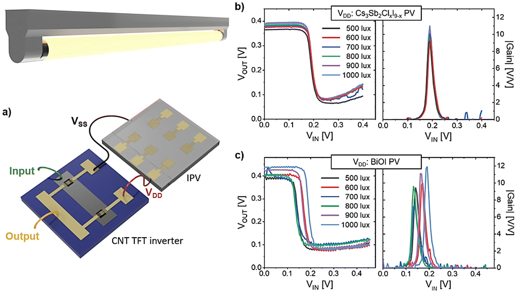 | ||
| Fig. 11 (a) Schematic of a printed TFT inverter connected to an IPV (the terminals labeled VSS and VDD correspond to the power supply terminals of the inverter) operated under FL lighting. Voltage transfer characteristics and voltage gain of the inverter powered by (b) Cs3Sb2ClxI9−x and (c) BiOI devices under FL illumination (with an illuminance of 500–1000 lux). Reproduced from ref. 211 with permission from [Wiley], copyright [2021]. | ||
| Year | Absorber material | Bandgap | Light source | Luminance (Lux) | MPD (μW cm−2) | PCE at artificial light (%) | PCE at solar spectrum (%) | Ref. |
|---|---|---|---|---|---|---|---|---|
| 2015 | CH3NH3PbI3−xClx | 1.6 | FL | 100 | — | 20.90 | — | 185 |
| 600 | — | 25.10 | ||||||
| 1000 | — | 26.30 | ||||||
| 2016 | MAPbI3 | 1.5 | CFL | 200 | 13.4 | 20.8 | 11.1 | 188 |
| 400 | 28.2 | 21.9 | ||||||
| LED | 200 | 11.6 | 17.4 | |||||
| 400 | 24.9 | 18.9 | ||||||
| 2017 | CH3NH3PbI3−xClx | — | LED | 200 | 7.2 | 10.80 | 9.2 | 189 |
| 400 | 16.0 | 12.10 | ||||||
| 2017 | MAPbI3 | 1.5 | LED | 200 | 9.77 | 12.85 | 14.8 | 212 |
| 400 | 19.2 | 13.32 | ||||||
| 2018 | CH3NH3PbI3 | 1.5 | LED | 200 | 20.2 | 25.0 | 19.0 | 190 |
| 400 | 41.6 | 26.9 | ||||||
| 2019 | CH3NH3PbI2.9Cl0.1 | 1.63 | LED | — | — | 20.80 | 13.3 | 53 |
| FL | — | — | 23.00 | |||||
| 2020 | CH3NH3PbI3 | 1.5 | LED | 200 | 12.36 | — | — | 187 |
| 400 | 28.03 | — | ||||||
| 800 | 63.79 | — | ||||||
| 1600 | 147.74 | — | ||||||
| FL | 200 | 56.43 | — | |||||
| 400 | 100.97 | — | ||||||
| 800 | 187.67 | — | ||||||
| 1600 | 376.85 | — | ||||||
| 2020 | BiOI | 1.94 | FL | 1000 | — | 4.4 | 0.9 | 211 |
| WLED | 1000 | — | 4.0 | |||||
| Cs3Sb2ClxI9−x | 1.95 | FL | 1000 | — | 4.9 | 1.2 | ||
| WLED | 1000 | — | 4.4 | |||||
| 2020 | Cs0.05FA0.83MA0.12PbI2.62Br0.38 | 1.6 | LED | 1000 | 98.8 | — | 16.28 | 213 |
| 2021 | CsPbBrI2 | 1.89 | LED | 1062 | 111.81 | 33.50 | 16.02 | 214 |
The indoor PSCs and outdoor PVs function in different areas of the spectrum and hence their design should consider some important aspects as follows: (i) The quality of the interfaces is crucial for good IPV performance and they should possess high shunt resistance and low series resistance. Fewer surface traps and leakage paths result in higher shunt resistance, which results in higher efficiency and lower reverse dark current under indoor illumination. Moreover, suitable band matching of the charge transport layers with the perovskites can effectively reduce trap-assisted recombination at the interfaces. Effective surface passivation strategies are thus important for good indoor performance of PSCs. (ii) p–i–n structures are less prone to hysteresis than n–i–p structures in the case of indoor PSCs.215 Moreover, in the inverted structure, the application of suitable HTM can lead to desired properties like high visible transmittance, matching of the band alignment with the perovskites, and high carrier mobility.(iii) Previous studies confirmed that planar-structured solar cells present better indoor performance than mesostructured cells as they show higher internal resistance under low light.
6. Encapsulation for IPV-powered IoTs
Innovative IoT-based solutions with low energy requirements are swiftly spreading across the globe. Since sensors, photodetectors, wireless nodes, and IoT-based devices all need nano- to milli-watts of electricity to operate smoothly, indoor solar cells integrated with them can act as power sources. These IoT devices need to be self-powered. They can be powered by indoor solar cells along with the battery or can be powered by IPV alone. Since IoT devices with indoor solar cells or modules will soon occupy the market, quick research is required to provide this industrial opportunity with an edge over the competition. The primary method for increasing the stability of IoT devices is by encapsulating them because this is one of the best ways to protect devices from thermal and chemical instabilities.216Encapsulation is very important for IoT devices powered by IPVs, as it prevents the toxic solar cell materials from affecting the end-users. The encapsulation technique can maintain the performance of IPVs while greatly extending their lifespan. Numerous methods and materials have been researched for encapsulating organic PVs and PSCs in single-layer and multilayer structures. Although physical encapsulation cannot reduce lead consumption, it can minimize lead leakage. Variable water vapor transmittance levels are regarded as an effective encapsulation method since they can extend the lifetime of indoor photovoltaics. Devices with an acrylic elastomer coating are not only water-resistant but also mechanically stretchable and adapt to fabrics and human skin.217 Organic solar cells covered by the elastomer on both sides kept 80% of their PCE after being submerged for 100 minutes and 20 cycles of being manually compressed by 52%.218 Essential criteria for the material/process selection include avoiding harmful solvents in the encapsulant, using a low-temperature deposition approach, and choosing a chemically inert layer for the layer beneath it. PSC encapsulation can significantly improve operational stability to levels tested in an N2 environment and other optimizations and techniques. Fluoropolymers and hydrophobic carbon electrodes have been utilized as encapsulants to allow PSCs to operate in non-inert environments. This technique was also used to stabilize perovskite solar panels for 1000 hours under IEC test criteria using polyolefin as an encapsulant.219 Due to concerns about the thermal breakage of the entire device stack, the encapsulation method has some disadvantages. Polyurethane has only been discussed as a potential encasing material for perovskite solar modules produced at a lower temperature of 80 °C.220 The projection for this technique comprises economical encapsulants with self-healing capacities and further developing simplified strategies to boost the stability of the perovskite solar module device. However, some factors, such as bulk perovskite stability and suitable encapsulation, must be considered to produce efficient indoor photovoltaic cells. More importantly, encapsulation must be affordable for IPV-powered IoTs to remain appealing and competitive.165 Moreover, encapsulation will be the final stage of manufacturing IPV-based IoT devices and it is largely dependent on the type of substrate.27 Encapsulated IPVs made on rigid substrates will increase their weight, whereas encapsulation of flexible IPVs will provide more compatibility and high power per weight ratio.
7. Toxicity issue
Photovoltaics (PV) will rule the energy generation sector soon. The PV market has observed rapid growth with a compound annual growth rate (CAGR) of 34% between 2010 and 2020.221 Although PV technologies do not emit greenhouse gases and are considered green technologies, it is high time to assess the toxic effect of the PV cells/modules.222 The presence of toxic lead (Pb) in the perovskite composition raises major concerns over its indoor applications as indoor PSCs will be in close proximity to humans.223 Crystalline Si solar panels contain lead-based solder materials such as Sn–Pb and Sn–Pb–Ag alloys.224 Moreover, a-Si, GaAs-based solar cells mostly employ non-toxic materials while CdTe thin film solar cells contain toxic cadmium and CIGS suffers from indium toxicity.225The different constituents of a DSSC possess different levels of toxicity but the main concern typically arises due to the photosensitizer material.93 Ru-based complexes, QD sensitizers consisting of cadmium (Cd) and lead (Pb), and lead-based perovskite dyes are toxic in nature,226–228 but organic dyes, being metal-free, are non-toxic.229 Several liquid electrolytes such as acrylonitrile, metal-based compounds and certain CE can also be harmful. To tackle these toxicity challenges, recent research is focussing more on colloidal ternary or quaternary metal-free QD sensitizers, lead-free perovskite-based dyes and the development of quasi-solid electrolytes with high efficiency.230–234 The search for alternate less toxic, highly efficient counter electrode materials is also gaining greater research interest.235
Materials used in OPV are generally non-toxic in nature. However, the fabrication of OPV devices involve the use of toxic solvents such as cholorobenzene (CB), choloroform (CF), 1,2-dichlorobenzene (DCB), etc., which are harmful to both human health and the environment. This can be mitigated by utilising a suitable green solvent (chlorine-free, non-aromatic, and non-halogenated solvents) in the fabrication process.236
The next-generation perovskite solar cells with the greatest potential are primarily lead-based. In addition, in QD solar cells, PbS is one of the absorbing materials. Lead can affect all organs; however, the nervous system is the most vulnerable to lead toxicity. The lead exposed to the human body lastly gets deposited into the bones after traveling through the blood vessels and the soft tissues.142 This can severely affect normal metabolic activities and cause several health hazards to humans.237 Furthermore, long-time lead exposure can reduce male fertility and cause kidney and blood-related issues.238 On the other hand, cadmium can increase the risk of cancer, kidney dysfunction, and osteoporosis.239
The US Environmental Protection Agency (EPA) has set the upper limit for lead and cadmium contamination in drinking water to be 0.015 mg L−1 and 0.005 mg L−1, respectively.240 Park et al. estimated that 1 m2 perovskite solar module (considering 400 nm thick perovskite layer) contains approx. 0.4 g of lead, which is equivalent to the lead content of 1 m2 of natural soil with 1 cm2 thickness. Besides, the amount of lead in the perovskite solar module is less than one-fifth of the amount used in the c-Si solar module.241 However, the bioavailability of perovskite lead is many times higher than the other lead sources, which is of great concern.242
Contamination happens mainly due to the landfilling of dead solar panels, which is increasing every year. Apart from landfilling, cracks/damages in the installed solar panels due to natural calamities (hailstorms, cyclones etc.) result in contaminations.243 Lead from perovskite can dissolve in rainwater or evaporate at high temperatures. Su et al. reported that lead from perovskite solar cells dissolves in DI water, and the leaching concentration of Pb exceeds 5.0 mg L−1.244 Jiang et al. estimated lead leakage from broken perovskite solar modules in various simulated weather conditions. In extreme situations (water dripped, heated at 45 °C for 4 h, and then water dripped again), lead leakage in dripped water is as high as 28.3 mg L−1.245
Recently, researchers have been focusing on robust and safe encapsulation options to tackle this issue. One approach is the utilization of self-healing encapsulation to reduce lead leakage.245 Another approach is the use of lead adsorbent in the module structure.246–248 Besides preventing lead leakage during its lifetime, appropriate measures should be taken to recycle dead solar panels. The lead must be recovered from the panels before the final disposal. Binek et al. recovered PbI2 from perovskite solar cells using DMF and reused the PbI2 for fabricating fresh perovskite solar cells that gave a comparable performance.249 Park et al. recently prepared iron-containing hydroxyapatite with a strong negatively charged surface that absorbs Pb and has been demonstrated for Pb separation and recovery from perovskite-contaminated samples.250 Interestingly, many such efforts of lead recovery have been reported recently.251–253
8. Challenges and future prospects
Over time, continuous research and materials developments have been able to increase the device performances for various PV technologies. The PCEs of solar cells based on crystalline silicon (c-Si), amorphous silicon (a-Si), copper indium gallium selenide (CIGS), organic photovoltaics (OPV), perovskite solar cells (PSC), and dye-sensitized solar cells (DSSC) have improved a lot under outdoor conditions. Despite their reasonably good device performances under 1 sun, the a-Si, c-Si, and CIGS solar cells experience the issues of low photovoltage and reduced device performances under low light or indoor illumination conditions.28 However, OPV, PSC, and DSSC technologies are solution-processable, can be fabricated onto flexible and lightweight substrates, and can be easily customized depending upon the applications. These features enable OPVs, PSCs, and DSSCs to be used in indoor applications. Despite being the most recent photovoltaic technology, perovskite photovoltaics have been positioned as a highly efficient and low-cost PV technology. Due to the excellent optoelectronic properties of the perovskite material, the PSCs have surpassed OPVs and DSSCs in terms of efficiency and device performance. The growing market of IoT, the diverse applications of the PSCs, and the huge interest in the PSCs are increasing the attention of the perovskite solar cells in indoor applications.Although DSSCs have proved to be promising candidates for indoor photovoltaic systems, there are certain challenges. The high cost of ruthenium-based dyes, platinum counter electrodes, and transparent electrodes hinders large-scale commercialization.254,255 To minimize the toxicity issues associated with the electrolytes, several non-toxic electrolytes, such as ionic liquids have been employed in DSSCs.256,257 Apart from toxicity and stability management, the indoor light intensity needs to be carefully optimized to obtain maximum efficiency from the DSSCs. Also, the orientation (i.e. horizontal or vertical placing) of dye-based PV systems affects the overall performance and stability.258 Besides, the liquid electrolytes give rise to leakage problems that can severely hamper the structural balance of the device. Recently, quasi-solid or solid-state electrolytes (QSE) have been incorporated to solve the issue.259 In QSE, the electrolyte has both cohesive and diffusive transport properties like that of a solid and liquid. Apart from QSE, solid-state hole transport materials (HTMs) have been utilized in DSSCs to avoid leakage and efficiency loss.260 Solid-state materials can be either organic or inorganic. The solid-state DSSCs usually exhibit low efficiency due to electrically weak contact between the dye and electrodes, resulting in poor dye regeneration.261 Owing to their solid nature, hole transportation is obstructed, which increases the series resistance and thus lowers efficiency.262 Moreover, the large-scale fabrication of DSSC is also hindered due to the toxicity of Ru-based dyes. The manufacturing cost, which depends on the material including the substrate, dye, and electrolyte, also poses a barrier to commercialization. Thus, reducing the overall fabrication cost has been a prime research focus over the years.
The performance of OPVs cells under outdoor conditions and their degradation mechanism have been extensively studied but their performance under low light irradiance conditions still needs to be addressed to make IOPV cells commercially viable. Fullerene and its derivatives are the most common acceptor materials in OPVs. Their degradation upon prolonged exposure to moisture, heat, and light, as well as their parasitic resistance, remains the main challenge for OPV cells.263 Non-fullerene materials can be used as an alternative acceptor material to overcome these issues. In addition, the majority of the studies on organic photovoltaics under indoor conditions have used LED or fluorescent lamps as a light source. There have been limited studies that consider alternative indoor light sources such as halogen lamps. Moreover, it has been reported that organic photovoltaics under halogen lamps show less PCE as compared to LED and under 1 sun conditions.137 Therefore, finding suitable photoactive layer materials with an absorption profile matching the emission spectra of indoor light sources is critical for obtaining higher PCE in the case of IOPV. Furthermore, impurities in IOPV due to additional dopant material induce trap states and they act as a recombination centre.144 This further reduces the device's performance. VOC loss under artificial lighting is the main challenge in an indoor environment. A comprehensive understanding of the VOC loss cell designed for indoor application is still lacking. To obtain high VOC, proper alignment of donor and acceptor energy levels should be ensured.
Bandgap tunability enables quantum dot solar cells that are suitable for indoor light-harvesting applications. Furthermore, solution-processability makes device fabrication feasible. More importantly, unlike organic or hybrid solar cells, quantum dot solar cells are stable for a long period. However, in terms of PCE, QDSCs lag behind as compared to perovskite solar cells. Another challenge is to find suitable lead-free QDs for this particular application. Moreover, more studies regarding the indoor application of QDSCs are required for better understanding.32,165
On the other hand, perovskite photovoltaics as the next-generation PV technology have emerged as promising candidates for indoor applications owing to the unique material properties of perovskites.264 It is also evident from previous studies that under weak light intensity, PSCs can deliver high PCE along with maintaining high VOC.49,183 Besides the high efficiency and the well-matched spectral response in indoor illuminance levels, PSCs possess the advantages of solution-processability, low-cost fabrication, bandgap tunability, and mechanical flexibility, which allow them to be used in different custom applications. Several studies on the performances of PSCs in indoor illumination conditions have been published very recently and it seems that the interest in this field is growing very fast. The reported high efficiencies and the device lifetimes have shown enormous potential for the PSCs to be applied for a range of diverse indoor PV applications. However, there are certain challenges for indoor PSCs that need to be properly addressed to achieve commercial success, which mainly include the toxicity and environmental stability of PSCs. The presence of lead in the perovskite composition raises the toxicity issue, which is more sensitive in the case of IPVs.223 Furthermore, the poor environmental stability of the perovskite layer, i.e., the degradation and the phase change of the perovskite active layer in the presence of moisture, heat, oxygen, etc. degrade the performance of the devices and can induce the leakage of PbI2 to the environment.201,265 Therefore, to enhance environmental stability and tackle the toxicity issue, advanced encapsulation techniques should be incorporated. To realize Pb-free PSCs, intensive research is being conducted and wide bandgap lead-free material Sn-based and Bi-based perovskites have been applied but they still lag in terms of efficiency.266,267 For fabricating a high-efficiency indoor solar cell, a wide bandgap active layer is necessary. Effective bandgap engineering on both the cation part and anion part of the perovskites is required to tune the requisite properties for high efficiency and stability of PSCs. Also, considering the average lifetime of the household device with which the PSC is connected and the less severe environmental effects (much lower intensity than the outdoor, with no UV and rain) inside, the indoor PSCs can offer much longer lifetimes than PSCs operating outdoors and so they are likely to be commercialized very soon.
Solution-processable IPVs offer ease of fabrication, low cost, high power densities, flexibility, and standalone features, which accelerate the development of autonomous IoT and future wearable devices. Although the performance of DSSCs under full sunlight lags behind that of PSCs and OSCs, the same cannot be said for indoor artificial illumination conditions. In indoor lighting conditions, DSSCs have performed significantly well with power conversion efficiencies above 30% (record efficiency of 34.5%).89 The efficient low- light harvesting at low cost makes DSSCs attractive third-generation PV technology for powering small indoor electronic devices.32,268 Compared to conventional PV technology, DSSCs and OPVs can more effectively meet the requirements (both functional and aesthetic value) for many applications including building integrated photovoltaics and small IoT devices etc.269 An example of the application of solution-processed solar cells is the integration of solar panels into glass facades of buildings to power the building. The light weight, flexibility, and color tunability properties of OPV and DSSC enable them to be attractive IPV technology for application on buildings. Another possible approach is to integrate IPV modules in public places (bus shelters, train station etc.) where along with providing power in the dark, it can also provide power to sensors (to probe temperature, air quality etc.) and hardware for real-time traffic monitoring systems, etc. By taking advantage of various fabrication techniques, researchers have focused on the integration of flexible OPV, DSSC, and PSC on various wearable such as garments, bags, wrist watches, etc. Moreover, for indoor applications, DSSCs and OPVs have been successfully integrated on various indoor IoT devices such as the computer mouse, remote controls, indoor lighting systems etc., and PSCs are making their way towards these applications. However, solution-processed IPVs should ensure the delivery of sufficient output power to drive commercially available IoT devices for indoor applications such as self-powered sensors, Wi-Fi modules, microcontrollers, etc.
The works on IPVs have been succeeded by the works on PV for outdoor. The researchers were at first mainly focused on investigating the indoor performance utilizing similar absorbers. Substantial investigations have been carried out on indoor DSSCs and IOPVs and most of them used wide bandgap materials, as reflected in Tables 1 and 2. Comparatively, much less work has been done on indoor PSCs. It is worth noting that the incorporation of bromine in halide perovskites increases its bandgap but it suffers from halide segregation issues. Moreover, inorganic perovskites have phase stability issues. Still, researchers are addressing these challenges and reports using wide bandgap perovskites for indoor applications are being produced. Recently, the Miyasaka group reported the application of CsPbI2Br (bandgap = 1.92 eV) and achieved more than 34% efficiency in LED illumination.205 Similar reports are expected in the future.
Another issue with indoor PV is that no universal light source exists for indoor applications. Different indoor light sources show different emission spectra, power densities, etc. Moreover, under real indoor conditions, the diffused sunlight has to be taken into account during the daytime.160 At present, there is no testing standard for reporting the performances of indoor PV. It is necessary to have a common standard for reporting the efficiencies of the PSCs and also the device stability tests under indoor conditions need to follow a standard protocol. Since the performance of the IPV depends on the type of light source, light intensity, lighting designs, etc., proper IPV design, selection of materials, and the device structure have to be conducted accordingly to ensure maximum output. Therefore, designing new synthetic materials with suitable bandgaps and spectral matching (for optimized light sources) is the need of the hour. Proper simulation tools need to be implemented to effectively address special indoor light-related issues, such as differences in light sources, advanced lighting designs, device characteristics under low light, and product integration. A multidisciplinary approach is required for the fast development of IPV-based products involving materials scientists, architects, illumination engineers, IoT experts, device engineers, and other professionals from industry and academia, because the IPV-based IoT market will see a massive expansion in coming years. Also, there is room for further improvements in terms of the efficiency and stability of solution-processed next-generation PV technologies under indoor illumination and hence further research is required in this regard. Cost reduction in the materials and efficient fabrication processes need to be realized for the next generation of indoor solar cells. Efficient passivation strategies need to be implemented to obtain better indoor performances. Although the IPV market is smaller than the established solar power market, the expected growth of IPV-powered devices and the advancement of emerging PV technologies will supplement each other in their way of successful commercialization. We hope that the current growth in the IoT market will fuel the interest in indoor solution-processed next-generation photovoltaics and further research will lead to their successful commercialization very soon.
Conflicts of interest
There are no conflicts to declare.Acknowledgements
S. M., S. G., B. B., M. P., H. D. would like to acknowledge Indian Institute of Technology Kharagpur for research fellowship and S. P. and D. K. would like to acknowledge Prime Minister Research Fellowship for funding and India Institute of Technology Kharagpur for research facility. T.S. would like to acknowledge Science and Engineering Research Board for funding support (Grant No. SRG/2019/1303 and IPA/2021/000081) and IIT Kharagpur for infrastructure facility.References
- D. Archer, Global warming: understanding the forecast, John Wiley & Sons, 2011 Search PubMed.
- The trillion-dollar opportunity for the industrial sector: How to extract full value from technology|McKinsey, https://www.mckinsey.com/business-functions/mckinsey-digital/our-insights/the-trillion-dollar-opportunity-for-the-industrial-sector, accessed 7 May 2021.
- K. E. Jeon, J. She, P. Soonsawad and P. C. Ng, IEEE Internet Things J., 2018, 5, 811–828 Search PubMed.
- A. Nasiri, S. A. Zabalawi and G. Mandic, IEEE Trans. Ind. Electron., 2009, 56, 4502–4509 Search PubMed.
- H. Jayakumar, K. Lee, S. Lee, A. Raha, Y. Kim and V. Raghunathan, Proceedings of the 2014 international symposium on Low power electronics and design, ACM, New York, NY, USA.
- C. K. Ho and R. Zhang, IEEE Transactions on Signal Processing, 2012, vol. 60, pp. 4808–4818 Search PubMed.
- J. Yan, X. Liao, D. Yan and Y. Chen, Review of Micro Thermoelectric Generator, Institute of Electrical and Electronics Engineers Inc., 2018, vol. 27 Search PubMed.
- C. Wu, A. C. Wang, W. Ding, H. Guo and Z. L. Wang, Triboelectric Nanogenerator: A Foundation of the Energy for the New Era, 2019, vol. 9 Search PubMed.
- F. G. Montoya, A. Peña-García, A. Juaidi and F. Manzano-Agugliaro, Energy Build., 2017, 140, 50–60 CrossRef.
- S. Ulukus, A. Yener, E. Erkip, O. Simeone, M. Zorzi, P. Grover and K. Huang, IEEE J. Sel. Areas Commun., 2015, 33, 360–381 Search PubMed.
- G. Apostolou, A. Reinders and M. Verwaal, Energy Sci. Eng., 2016, 4, 69–85 CrossRef.
- M. F. Müller, M. Freunek and L. M. Reindl, IEEE J. Photovoltaics, 2013, 3, 59–64 Search PubMed.
- S. Mishra, S. Ghosh and T. Singh, ChemSusChem, 2021, 14, 512–538 CrossRef CAS PubMed.
- J. Gong, K. Sumathy, Q. Qiao and Z. Zhou, Renewable Sustainable Energy Rev., 2017, 68, 234–246 CrossRef CAS.
- P. Ferdowsi, Y. Saygili, F. Jazaeri, T. Edvinsson, J. Mokhtari, S. M. Zakeeruddin, Y. Liu, M. Grätzel and A. Hagfeldt, ChemSusChem, 2020, 13, 212–220 CrossRef CAS PubMed.
- M. Privado, H. Dahiya, P. De La Cruz, M. L. Keshtov, F. Langa and G. D. Sharma, J. Mater. Chem. C, 2021, 9, 16272–16281 RSC.
- N. K. Elumalai and A. Uddin, Energy Environ. Sci., 2016, 9, 391–410 RSC.
- E. H. Sargent, Nat. Photonics, 2012, 6, 133–135 CrossRef CAS.
- I. J. Kramer, J. C. Minor, G. Moreno-Bautista, L. Rollny, P. Kanjanaboos, D. Kopilovic, S. M. Thon, G. H. Carey, K. Wei Chou, D. Zhitomirsky, A. Amassian, E. H. Sargent, I. J. Kramer, J. C. Minor, G. Moreno-Bautista, L. Rollny, P. Kanjanaboos, D. Kopilovic, S. M. Thon, G. H. Carey, D. Zhitomirsky, E. H. Sargent, K. W. Chou and A. Amassian, Adv. Mater., 2015, 27, 116–121 CrossRef CAS PubMed.
- P. Wang, Y. Wu, B. Cai, Q. Ma, X. Zheng and W. H. Zhang, Adv. Funct. Mater., 2019, 29, 1807661 CrossRef CAS.
- T. Singh, Y. Udagawa, M. Ikegami, H. Kunugita, K. Ema and T. Miyasaka, APL Mater., 2017, 5, 016103 CrossRef.
- H. K. H. Lee, J. Barbé and W. C. Tsoi, Solar Cells and Light Management: Materials, Strategies and Sustainability, Elsevier, 2019, pp. 355–388 Search PubMed.
- B. Minnaert and P. Veelaert, Energies, 2014, vol. 7, pp. 1500–1516 Search PubMed.
- L. K. Jagadamma and S. Wang, Front. Chem., 2021, 9, 71 Search PubMed.
- A. Kar and A. Kar, 1st Int. Conf. Autom. Control. Energy Syst. – 2014, ACES 2014 DOI:10.1109/ACES.2014.6807997.
- I. Mathews, S. N. Kantareddy, T. Buonassisi and I. M. Peters, Joule, 2019, 3, 1415–1426 CrossRef CAS.
- C. Polyzoidis, K. Rogdakis and E. Kymakis, Adv. Energy Mater., 2021, 11, 2101854 CrossRef CAS.
- S. Kim, M. Jahandar, J. H. Jeong and D. C. Lim, Curr. Altern. Energy, 2019, 3, 3–17 CrossRef.
- D. Saranin, T. Komaricheva, L. Luchnikov, D. S. Muratov, T. S. Le, Y. Karpov, P. Gostishchev, S. Yurchuk, D. Kuznetsov, S. Didenko and A. Di Carlo, Sol. Energy Mater. Sol. Cells, 2021, 227, 111095 CrossRef CAS.
- I. Mathews, S. N. R. Kantareddy, S. Sun, M. Layurova, J. Thapa, J. Correa-Baena, R. Bhattacharyya, T. Buonassisi, S. Sarma and I. M. Peters, Adv. Funct. Mater., 2019, 29, 1904072 CrossRef CAS.
- K. Wojciechowski, D. Forgács and T. Rivera, Sol. RRL, 2019, 3, 1900144 CrossRef.
- B. Li, B. Hou and G. A. J. Amaratunga, InfoMat, 2021, 3, 445–459 CrossRef CAS.
- M. Graetzel, R. A. J. Janssen, D. B. Mitzi and E. H. Sargent, Nature, 2012, 488, 304–312 CrossRef CAS PubMed.
- V. Pecunia, L. G. Occhipinti and R. L. Z. Hoye, Adv. Energy Mater., 2021, 11, 2100698 CrossRef CAS.
- A. Venkateswararao, J. K. W. Ho, S. K. So, S. W. Liu and K. T. Wong, Mater. Sci. Eng., R, 2020, 139, 100517 CrossRef.
- S. Biswas and H. Kim, Polymers, 2020, 12, 1338 CrossRef CAS PubMed.
- M. Wu, C. Kuo, L. Jhuang, P. Chen, Y. Lai and F. Chen, Adv. Energy Mater., 2019, 9, 1901863 CrossRef CAS.
- Y. Cui, H. Yao, T. Zhang, L. Hong, B. Gao, K. Xian, J. Qin and J. Hou, Adv. Mater., 2019, 31, 1904512 CrossRef CAS PubMed.
- A. Virtuani, E. Lotter and M. Powalla, Sol. Energy Mater. Sol. Cells, 2006, 90, 2141–2149 CrossRef CAS.
- C. P. Standards, Handbook of Applied Photometry, 1997.
- M. Müller, J. Wienold, W. D. Walker and L. M. Reindl, Conf. Rec. IEEE Photovolt. Spec. Conf., 2009, pp. 000738–000743.
- International Standards|CIE, https://cie.co.at/publications/international-standards, (accessed 12 September 2022).
- L. T. Sharpe, A. Stockman, W. Jagla and H. Jaägle, J. Vis., 2005, 5, 3 CrossRef PubMed.
- L. Bellia, F. Bisegna and G. Spada, Build. Environ., 2011, 46, 1984–1992 CrossRef.
- J. K. W. Ho, H. Yin and S. K. So, J. Mater. Chem. A, 2020, 8, 1717–1723 RSC.
- F. Zhao, S. Dai, Y. Wu, Q. Zhang, J. Wang, L. Jiang, Q. Ling, Z. Wei, W. Ma, W. You, C. Wang and X. Zhan, Adv. Mater., 2017, 29, 1700144 CrossRef PubMed.
- C. Sun, F. Pan, H. Bin, J. Zhang, L. Xue, B. Qiu, Z. Wei, Z. G. Zhang and Y. Li, Nat. Commun., 2018, 9, 1–10 CrossRef PubMed.
- Y. Cui, L. Hong and J. Hou, ACS Appl. Mater. Interfaces, 2020, 12, 38815–38828 CrossRef CAS PubMed.
- T. Singh, S. Öz, A. Sasinska, R. Frohnhoven, S. Mathur and T. Miyasaka, Adv. Funct. Mater., 2018, 28, 1706287 CrossRef.
- W. Tress, Adv. Energy Mater., 2017, 7, 1602358 CrossRef.
- W. Shockley and W. T. Read, Phys. Rev., 1952, 87, 835 CrossRef CAS.
- W. Tress, M. Yavari, K. Domanski, P. Yadav, B. Niesen, J. P. Correa Baena, A. Hagfeldt and M. Graetzel, Energy Environ. Sci., 2018, 11, 151–165 RSC.
- L. K. Jagadamma, O. Blaszczyk, M. T. Sajjad, A. Ruseckas and I. D. W. Samuel, Sol. Energy Mater. Sol. Cells, 2019, 201, 110071 CrossRef CAS.
- S. Porwal, M. Paul, H. Dixit, S. Mishra and T. Singh, Adv. Theory Simul., 2022, 5, 2200207 CrossRef CAS.
- S. Ryu, D. C. Nguyen, N. Y. Ha, H. J. Park, Y. H. Ahn, J. Y. Park and S. Lee, Sci. Rep., 2019, 9, 1–12 CrossRef CAS PubMed.
- W. Shockley and H. J. Queisser, J. Appl. Phys., 1961, 32, 510–519 CrossRef CAS.
- A. S. Teran, J. Wong, W. Lim, G. Kim, Y. Lee, D. Blaauw and J. D. Phillips, IEEE Trans. Electron Devices, 2015, 62, 2170–2175 CAS.
- L. K. Ma, Y. Chen, P. C. Y. Chow, G. Zhang, J. Huang, C. Ma, J. Zhang, H. Yin, A. M. Hong Cheung, K. S. Wong, S. K. So and H. Yan, Joule, 2020, 4, 1486–1500 CrossRef CAS.
- Y. W. Noh, I. S. Jin, K. S. Kim, S. H. Park and J. W. Jung, J. Mater. Chem. A, 2020, 8, 17163–17173 RSC.
- L. Cojocaru, S. Uchida, K. Tamaki, P. V. V. Jayaweera, S. Kaneko, J. Nakazaki, T. Kubo and H. Segawa, Sci. Rep., 2017, 7, 1–8 CrossRef CAS PubMed.
- C. L. Cutting, M. Bag and D. Venkataraman, J. Mater. Chem. C, 2016, 4, 10367–10370 RSC.
- N. H. Reich, W. G. J. H. M. van Sark and W. C. Turkenburg, Renewable Energy, 2011, 36, 642–647 CrossRef.
- T. Leijtens, S. D. Stranks, G. E. Eperon, R. Lindblad, E. M. J. Johansson, I. J. McPherson, H. Rensmo, J. M. Ball, M. M. Lee and H. J. Snaith, ACS Nano, 2014, 8, 7147–7155 CrossRef CAS PubMed.
- K. K. Chauhan, S. Prodhan, D. Ghosh, P. Waghale, S. Bhattacharyya, P. K. Dutta and P. K. Datta, IEEE J. Photovoltaics, 2020, 10, 803–810 Search PubMed.
- A. Miyata, A. Mitioglu, P. Plochocka, O. Portugall, J. T. W. Wang, S. D. Stranks, H. J. Snaith and R. J. Nicholas, Nat. Phys., 2015, 11, 582–587 Search PubMed.
- Y. M. Wang, S. Bai, L. Cheng, N. N. Wang, J. P. Wang, F. Gao, W. Huang, Y. M. Wang, L. Cheng, N. N. Wang, J. P. Wang, W. Huang, S. Bai and F. Gao, Adv. Mater., 2016, 28, 4532–4540 CrossRef CAS PubMed.
- K. Yoshikawa, H. Kawasaki, W. Yoshida, T. Irie, K. Konishi, K. Nakano, T. Uto, D. Adachi, M. Kanematsu, H. Uzu and K. Yamamoto, Nat. Energy, 2017, 2, 1–8 Search PubMed.
- G. Kim, G. Kim, J. W. Lim, J. W. Lim, J. Kim, J. Kim, S. J. Yun, S. J. Yun and M. A. Park, ACS Appl. Mater. Interfaces, 2020, 12, 27122–27130 CrossRef CAS PubMed.
- M. H. Kao, C. H. Shen, P. C. Yu, W. H. Huang, Y. L. Chueh and J. M. Shieh, Sci. Rep., 2017, 7, 1–8 CrossRef CAS PubMed.
- E. Moon, D. Blaauw and J. D. Phillips, IEEE Trans. Electron Devices, 2017, 64, 15–20 CAS.
- G. E. Bunea, K. E. Wilson, Y. Meydbray, M. P. Campbell and D. M. De Ceuster, Conf. Rec. 2006 IEEE 4th World Conf. Photovolt. Energy Conversion, WCPEC-4, 2006, 2, pp. 1312–1314.
- K. Ruhle and M. Kasemann, Conf. Rec. IEEE Photovolt. Spec. Conf., 2013, pp. 2651–2654.
- M. Foti, C. Tringali, A. Battaglia, N. Sparta, S. Lombardo and C. Gerardi, Sol. Energy Mater. Sol. Cells, 2014, 130, 490–494 CrossRef CAS.
- I. Mathews, G. Kelly, P. J. King and R. Frizzell, 2014 IEEE 40th Photovolt. Spec. Conf. PVSC 2014, 2014, pp. 510–513.
- I. Mathews, P. J. King, F. Stafford and R. Frizzell, IEEE J. Photovoltaics, 2016, 6, 230–235 Search PubMed.
- A. S. Teran, E. Moon, W. Lim, G. Kim, I. Lee, D. Blaauw and J. D. Phillips, IEEE Trans. Electron Devices, 2016, 63, 2820–2825 CAS.
- Q. Li, K. Shen, R. Yang, Y. Zhao, S. Lu, R. Wang, J. Dong and D. Wang, Sol. Energy, 2017, 157, 216–226 CrossRef CAS.
- C. Yang, R. P. Xue, X. Li, X. Q. Zhang and Z. Y. Wu, Renewable Energy, 2020, 161, 836–845 CrossRef CAS.
- Y. Dai, H. Kum, M. A. Slocum, G. T. Nelson and S. M. Hubbard, 2017 IEEE 44th Photovoltaic Specialist Conference (PVSC), 2017, pp. 222–225 Search PubMed.
- B. O’Regan and M. Grätzel, Nature, 1991, 353, 737–740 CrossRef.
- A. Hagfeldt, G. Boschloo, L. Sun, L. Kloo and H. Pettersson, Chem. Rev., 2010, 110, 6595–6663 CrossRef CAS PubMed.
- Z. S. Wang, N. Koumura, Y. Cui, M. Takahashi, H. Sekiguchi, A. Mori, T. Kubo, A. Furube and K. Hara, Chem. Mater., 2008, 20, 3993–4003 CrossRef CAS.
- K. S. Keremane, I. M. Abdellah, P. Naik, A. El-Shafei and A. V. Adhikari, Phys. Chem. Chem. Phys., 2020, 22, 23169–23184 RSC.
- B. G. Kim, K. Chung and J. Kim, Chem. – Eur. J., 2013, 19, 5220–5230 CrossRef CAS PubMed.
- P. Meti, D. J. Park and Y. D. Gong, Dyes Pigm., 2019, 168, 357–368 CrossRef CAS.
- A. Slodek, D. Zych, G. Szafraniec-Gorol, P. Gnida, M. Vasylieva and E. Schab-Balcerzak, Materials, 2020, 13, 2292 CrossRef CAS PubMed.
- T. Sutradhar and A. Misra, ChemistrySelect, 2019, 4, 3697–3705 CrossRef CAS.
- S. S. Soni, K. B. Fadadu, J. V. Vaghasiya, B. G. Solanki, K. K. Sonigara, A. Singh, D. Das and P. K. Iyer, J. Mater. Chem. A, 2015, 3, 21664–21671 RSC.
- D. Zhang, M. Stojanovic, Y. Ren, Y. Cao, F. T. Eickemeyer, E. Socie, N. Vlachopoulos, J. E. Moser, S. M. Zakeeruddin, A. Hagfeldt and M. Grätzel, Nat. Commun., 2021, 12, 1–10 CrossRef CAS PubMed.
- H. Michaels, M. Rinderle, R. Freitag, I. Benesperi, T. Edvinsson, R. Socher, A. Gagliardi and M. Freitag, Chem. Sci., 2020, 11, 2895–2906 RSC.
- B. Pashaei, H. Shahroosvand, M. Graetzel and M. K. Nazeeruddin, Chem. Rev., 2016, 116, 9485–9564 CrossRef CAS PubMed.
- U. Mehmood, S. U. Rahman, K. Harrabi, I. A. Hussein and B. V. S. Reddy, Adv. Mater. Sci. Eng., 2014 DOI:10.1155/2014/974782.
- S. Shalini, R. Balasundaraprabhu, T. Satish Kumar, N. Prabavathy, S. Senthilarasu and S. Prasanna, Int. J. Energy Res., 2016, 40, 1303–1320 CrossRef CAS.
- G. C. Vougioukalakis, A. I. Philippopoulos, T. Stergiopoulos and P. Falaras, Coord. Chem. Rev., 2011, 255, 2602–2621 CrossRef CAS.
- A. Abbotto and N. Manfredi, Dalton Trans., 2011, 40, 12421–12438 RSC.
- T. K. Chang and Y. Chi, RSC Adv., 2017, 7, 42013–42023 RSC.
- T. Higashino and H. Imahori, Dalton Trans., 2014, 44, 448–463 RSC.
- Y. C. Liu, H. H. Chou, F. Y. Ho, H. J. Wei, T. C. Wei and C. Y. Yeh, J. Mater. Chem. A, 2016, 4, 11878–11887 RSC.
- K. S. K. Reddy, Y. C. Liu, H. H. Chou, K. Kala, T. C. Wei and C. Y. Yeh, ACS Appl. Mater. Interfaces, 2018, 10, 39970–39982 CrossRef CAS PubMed.
- T. Bessho, S. M. Zakeeruddin, C. C.-Y. Yeh, E. Wei-Guang Diau, M. Grätzel, S. M. Zakeeruddin, M. Grätzel, C. C.-Y. Yeh and E. W.-G. Diau, Angew. Chem., Int. Ed., 2010, 49, 6646–6649 CrossRef CAS PubMed.
- K. Srinivas, K. Yesudas, K. Bhanuprakash, V. J. Rao and L. Giribabu, J. Phys. Chem. C, 2009, 113, 20117–20126 CrossRef CAS.
- H. Cha, D. S. Chung, S. Y. Bae, M. J. Lee, T. K. An, J. Hwang, K. H. Kim, Y. H. Kim, D. H. Choi and C. E. Park, Adv. Funct. Mater., 2013, 23, 1556–1565 CrossRef CAS.
- C. L. Wang, J. W. Shiu, Y. N. Hsiao, P. S. Chao, E. Wei-Guang Diau and C. Y. Lin, J. Phys. Chem. C, 2014, 118, 27801–27807 CrossRef CAS.
- C. L. Wang, P. T. Lin, Y. F. Wang, C. W. Chang, B. Z. Lin, H. H. Kuo, C. W. Hsu, S. H. Tu and C. Y. Lin, J. Phys. Chem. C, 2015, 119, 24282–24289 CrossRef CAS.
- M. C. Tsai, C. C. L. Wang, C. W. Chang, C. W. Hsu, Y. H. Hsiao, C. L. Liu, C. C. L. Wang, S. Y. Lin and C. Y. Lin, J. Mater. Chem. A, 2018, 6, 1995–2003 RSC.
- Y. S. Tingare, N. S. Vinh, H. H. Chou, Y. C. Liu, Y. S. Long, T. C. Wu, T. C. Wei and C. Y. Yeh, Adv. Energy Mater., 2018, 8, 1802405 CrossRef.
- T. Weil, T. Vosch, J. Hofkens, K. Peneva and K. Müllen, Angew. Chem., Int. Ed., 2010, 49, 9068–9093 CrossRef CAS PubMed.
- L. Chen, C. Li and K. Müllen, J. Mater. Chem. C, 2014, 2, 1938–1956 RSC.
- H. H. Chou, Y. C. Liu, G. Fang, Q. K. Cao, T. C. Wei and C. Y. Yeh, ACS Appl. Mater. Interfaces, 2017, 9, 37786–37796 CrossRef CAS PubMed.
- M. B. Desta, N. S. Vinh, C. Pavan Kumar, S. Chaurasia, W. T. Wu, J. T. Lin, T. C. Wei and E. Wei-Guang Diau, J. Mater. Chem. A, 2018, 6, 13778–13789 RSC.
- M. L. Jiang, J. J. Wen, Z. M. Chen, W. H. Tsai, T. C. Lin, T. J. Chow and Y. J. Chang, ChemSusChem, 2019, 12, 3654–3665 CrossRef CAS PubMed.
- M. Freitag, J. Teuscher, Y. Saygili, X. Zhang, F. Giordano, P. Liska, J. Hua, S. M. Zakeeruddin, J. E. Moser, M. Grätzel and A. Hagfeldt, Nat. Photonics, 2017, 11, 372–378 CrossRef CAS.
- C. T. Li, Y. L. Kuo, C. P. Kumar, P. T. Huang and J. T. Lin, J. Mater. Chem. A, 2019, 7, 23225–23233 RSC.
- Y. Cao, Y. Liu, S. M. Zakeeruddin, A. Hagfeldt and M. Grätzel, Joule, 2018, 2, 1108–1117 CrossRef CAS.
- E. Tanaka, H. Michaels, M. Freitag and N. Robertson, J. Mater. Chem. A, 2020, 8, 1279–1287 RSC.
- S. Ito and K. Takahashi, Int. J. Photoenergy, 2012 DOI:10.1155/2012/915352.
- B. Janne Halme, P. Vahermaa, K. Miettunen, P. Lund, J. Halme, P. Vahermaa, K. Miettunen and P. Lund, Adv. Mater., 2010, 22, E210–E234 CrossRef PubMed.
- M. Kokkonen, P. Talebi, J. Zhou, S. Asgari, S. A. Soomro, F. Elsehrawy, J. Halme, S. Ahmad, A. Hagfeldt and S. G. Hashmi, J. Mater. Chem. A, 2021, 9, 10527–10545 RSC.
- J. L. Lan, T. C. Wei, S. P. Feng, C. C. Wan and G. Cao, J. Phys. Chem. C, 2012, 116, 25727–25733 CrossRef CAS.
- W. Xiang and W. Tress, Adv. Mater., 2019, 31, 1–28 CrossRef PubMed.
- N. Vlachopoulos, A. Hagfeldt, I. Benesperi, M. Freitag, G. Hashmi, G. Jia, R. A. Wahyuono, J. Plentz and B. Dietzek, Sustainable Energy Fuels, 2021, 5, 367–383 RSC.
- J. H. Yum, E. Baranoff, F. Kessler, T. Moehl, S. Ahmad, T. Bessho, A. Marchioro, E. Ghadiri, J. E. Moser, C. Yi, M. K. Nazeeruddin and M. Grätzel, Nat. Commun., 2012, 3, 1–8 CrossRef PubMed.
- H. Jiang, Y. Ren, W. Zhang, Y. Wu, E. C. Socie, B. I. Carlsen, J. Moser, H. Tian, S. M. Zakeeruddin, W. Zhu and M. Grätzel, Angew. Chem., 2020, 132, 9410–9415 CrossRef.
- Y. S. Tingare, N. S. Vinh, H.-H. Chou, Y.-C. Liu, Y.-S. Long, T.-C. Wu, T.-C. Wei and C.-Y. Yeh, Adv. Energy Mater., 2017, 7, 1700032 CrossRef.
- M. A. Fusella, Y. L. Lin and B. P. Rand, Handbook of Organic Materials for Electronic and Photonic Devices, 2019, pp. 665–693 Search PubMed.
- M. Riede, B. Lüssem and K. Leo, Compr. Semicond. Sci. Technol., 2011, 1–6, 448–507 Search PubMed.
- N. Espinosa, F. O. Lenzmann, S. Ryley, D. Angmo, M. Hösel, R. R. Søndergaard, D. Huss, S. Dafinger, S. Gritsch, J. M. Kroon, M. Jørgensen and F. C. Krebs, J. Mater. Chem. A, 2013, 1, 7037–7049 RSC.
- B. A. Gregg, J. Phys. Chem. B, 2003, 107, 4688–4698 CrossRef CAS.
- C. W. Tang, Appl. Phys. Lett., 1998, 48, 183 CrossRef.
- F. C. Chen, Adv. Opt. Mater., 2019, 7, 1800662 CrossRef.
- M. Zhang, L. Zhu, G. Zhou, T. Hao, C. Qiu, Z. Zhao, Q. Hu, B. W. Larson, H. Zhu, Z. Ma, Z. Tang, W. Feng, Y. Zhang, T. P. Russell and F. Liu, Nat. Commun., 2021, 12, 1–10 CrossRef PubMed.
- S. Mori, T. Gotanda, Y. Nakano, M. Saito, K. Todori and M. Hosoya, Jpn. J. Appl. Phys., 2015, 54, 071602 CrossRef.
- H. Hoppe and N. S. Sariciftci, J. Mater. Res., 2004, 19, 1924–1945 CrossRef CAS.
- Y.-J. You, C. Eun Song, Q. Viet Hoang, Y. Kang, J. Soo Goo, D.-H. Ko, J.-J. Lee, W. Suk Shin, J. Won Shim, Y. You, J. S. Goo, J. W. Shim, C. E. Song, Q. V. Hoang, W. S. Shin, Y. Kang, D. Ko and J. Lee, Adv. Funct. Mater., 2019, 29, 1901171 CrossRef.
- C. H. Chen, H. C. Ting, Y. Z. Li, Y. C. Lo, P. H. Sher, J. K. Wang, T. L. Chiu, C. F. Lin, I. S. Hsu, J. H. Lee, S. W. Liu and K. T. Wong, ACS Appl. Mater. Interfaces, 2019, 11, 8337–8349 CrossRef CAS PubMed.
- M. Mainville and M. Leclerc, ACS Energy Lett., 2020, 5, 1186–1197 CrossRef CAS.
- M. A. Saeed, S. Cheng, S. Biswas, S. H. Kim, S. K. Kwon, H. Kim, Y. H. Kim and J. W. Shim, J. Power Sources, 2022, 518, 230782 CrossRef CAS.
- C. A. Reynaud, R. Clerc, P. B. Lechêne, M. Hébert, A. Cazier and A. C. Arias, Sol. Energy Mater. Sol. Cells, 2019, 200, 110010 CrossRef CAS.
- Y. Zhang, H. Yi, A. Iraqi, J. Kingsley, A. Buckley, T. Wang and D. G. Lidzey, Sci. Rep., 2017, 7, 1–9 CrossRef PubMed.
- S. Y. Park, Y. Li, J. Kim, T. H. Lee, B. Walker, H. Y. Woo and J. Y. Kim, ACS Appl. Mater. Interfaces, 2018, 10, 3885–3894 CrossRef CAS PubMed.
- R. Steim, T. Ameri, P. Schilinsky, C. Waldauf, G. Dennler, M. Scharber and C. J. Brabec, Sol. Energy Mater. Sol. Cells, 2011, 95, 3256–3261 CrossRef CAS.
- M. Li, F. Igbari, Z. K. Wang and L. S. Liao, Indoor Thin-Film Photovoltaics: Progress and Challenges, 2020, vol. 10 Search PubMed.
- Y. W. Kim, J. S. Goo, T. H. Lee, B. R. Lee, S. C. Shin, H. Kim, J. W. Shim and T. G. Kim, J. Power Sources, 2019, 424, 165–175 CrossRef CAS.
- S. C. Shin, C. W. Koh, P. Vincent, J. S. Goo, J. H. Bae, J. J. Lee, C. Shin, H. Kim, H. Y. Woo and J. W. Shim, Nano Energy, 2019, 58, 466–475 CrossRef CAS.
- B. P. Lechêne, M. Cowell, A. Pierre, J. W. Evans, P. K. Wright and A. C. Arias, Nano Energy, 2016, 26, 631–640 CrossRef.
- Z. Chen, T. Wang, Z. Wen, P. Lu, W. Qin, H. Yin and X. T. Hao, ACS Energy Lett., 2021, 6, 3203–3211 CrossRef CAS.
- R. Arai, S. Furukawa, Y. Hidaka, H. Komiyama and T. Yasuda, ACS Appl. Mater. Interfaces, 2019, 11, 9259–9264 CrossRef CAS PubMed.
- H. K. H. Lee, J. Wu, J. Barbé, S. M. Jain, S. Wood, E. M. Speller, Z. Li, F. A. Castro, J. R. Durrant and W. C. Tsoi, J. Mater. Chem. A, 2018, 6, 5618–5626 RSC.
- R. Singh, C. L. Chochos, V. G. Gregoriou, A. D. Nega, M. Kim, M. Kumar, S. C. Shin, S. H. Kim, J. W. Shim and J. J. Lee, ACS Appl. Mater. Interfaces, 2019, 11, 36905–36916 CrossRef CAS PubMed.
- H. K. H. Lee, Z. Li, J. R. Durrant and W. C. Tsoi, Appl. Phys. Lett., 2016, 108, 253301 CrossRef.
- H. Yin, J. K. W. Ho, S. H. Cheung, R. J. Yan, K. L. Chiu, X. Hao and S. K. So, J. Mater. Chem. A, 2018, 6, 8579–8585 RSC.
- R. Singh, S. C. Shin, H. Lee, M. Kim, J. W. Shim, K. Cho and J. J. Lee, Chem. – Eur. J., 2019, 25, 6154–6161 CrossRef CAS PubMed.
- S. C. Shin, P. Vincent, J. H. Bae, J. J. Lee, M. Nam, D. H. Ko, H. Kim and J. W. Shim, Dyes Pigm., 2019, 163, 48–54 CrossRef CAS.
- Y. Cui, Y. Wang, J. Bergqvist, H. Yao, Y. Xu, B. Gao, C. Yang, S. Zhang, O. Inganäs, F. Gao and J. Hou, Nat. Energy, 2019, 4, 768–775 CrossRef CAS.
- Z. Ding, R. Zhao, Y. Yu and J. Liu, J. Mater. Chem. A, 2019, 7, 26533–26539 RSC.
- M. Nam, J. Han, J. J. Kang, J. Shin, J. Na, Y. Park, J. Cho, B. Kim, H. H. Lee, R. Chang, D. H. D. D.-H. Ko, H. Hwi Lee, R. Chang, D. H. D. D.-H. Ko, M. Nam, J. Han, J. J. Kang, J. Shin, J. Cho, B. Kim, D. H. D. D.-H. Ko, J. Na, Y. Park, R. Chang and H. H. Lee, Adv. Energy Mater, 2019, 9, 1901856 CrossRef.
- M. Nam, C. Lee and D. H. Ko, Chem. Eng. J., 2022, 438, 135576 CrossRef CAS.
- N. W. Teng, S. S. Yang and F. C. Chen, IEEE J. Photovoltaics, 2018, 8, 752–756 Search PubMed.
- S. S. Yang, Z. C. Hsieh, M. L. Keshtov, G. D. Sharma and F. C. Chen, Sol. RRL, 2017, 1, 1700174 CrossRef.
- L. Xie, J. Zhang, W. Song, L. Hong, J. Ge, P. Wen, B. Tang, T. Wu, X. Zhang, Y. Li and Z. Ge, ACS Appl. Mater. Interfaces, 2021, 13, 20405–20416 CrossRef CAS PubMed.
- H. Il Je, E. Y. Shin, K. J. Lee, H. Ahn, S. Park, S. H. Im, Y. H. Kim, H. J. Son and S. K. Kwon, ACS Appl. Mater. Interfaces, 2020, 12, 23181–23189 CrossRef PubMed.
- J. Wu, S. Chen, A. Seeds and H. Liu, J. Phys. D: Appl. Phys., 2015, 48, 363001 CrossRef.
- X. Lan, O. Voznyy, A. Kiani, F. Pelayo García de Arquer, A. Saud Abbas, G.-H. Kim, M. Liu, Z. Yang, G. Walters, J. Xu, M. Yuan, Z. Ning, F. Fan, P. Kanjanaboos, I. Kramer, D. Zhitomirsky, P. Lee, A. Perelgut, S. Hoogland, E. H. Sargent, X. Lan, O. Voznyy, A. Kiani, F. P. García de Arquer, A. S. Abbas, G. Kim, M. Liu, Z. Yang, G. Walters, J. Xu, M. Yuan, F. Fan, P. Kanjanaboos, I. Kramer, D. Zhitomirsky, P. Lee, A. Perelgut, S. Hoogland, E. H. Sargent and Z. Ning, Adv. Mater., 2016, 28, 299–304 CrossRef CAS PubMed.
- B. Li, M. Lu, J. Feng, J. Zhang, P. M. Smowton, J. I. Sohn, I. K. Park, H. Zhong and B. Hou, J. Mater. Chem. C, 2020, 8, 10676–10695 RSC.
- X. Hou, Y. Wang, H. K. H. Lee, R. Datt, N. Uslar Miano, D. Yan, M. Li, F. Zhu, B. Hou, W. C. Tsoi and Z. Li, J. Mater. Chem. A, 2020, 8, 21503–21525 RSC.
- M. Otsuka, Y. Kurokawa, Y. Ding, F. B. Juangsa, S. Shibata, T. Kato and T. Nozaki, RSC Adv., 2020, 10, 12611–12618 RSC.
- B. Hou, B. S. Kim, H. K. H. Lee, Y. Cho, P. Giraud, M. Liu, J. Zhang, M. L. Davies, J. R. Durrant, W. C. Tsoi, Z. Li, S. D. Dimitrov, J. I. Sohn, S. N. Cha and J. M. Kim, Adv. Funct. Mater., 2020, 30, 2004563 CrossRef CAS.
- A. Kojima, K. Teshima, Y. Shirai and T. Miyasaka, J. Am. Chem. Soc., 2009, 131, 6050–6051 CrossRef CAS PubMed.
- Best Research-Cell Efficiency Chart|Photovoltaic Research|NREL, https://www.nrel.gov/pv/cell-efficiency.html, (accessed 6 May 2020).
- P. Pattanayak, P. Singh, N. K. Bansal, M. Paul, H. Dixit, S. Porwal, S. Mishra and T. Singh, J. Environ. Chem. Eng., 2022, 10, 108429 CrossRef CAS.
- Y. Liu, Z. Yang, D. Cui, X. Ren, J. Sun, X. Liu, J. Zhang, Q. Wei, H. Fan, F. Yu, X. Zhang, C. Zhao, S. Liu, Y. Liu, Z. Yang, D. Cui, X. Ren, J. Sun, X. Liu, J. Zhang, Q. Wei, H. Fan, F. Yu, X. Zhang, C. Zhao and S. Liu, Adv. Mater., 2015, 27, 5176–5183 CrossRef CAS PubMed.
- D. Shi, V. Adinolfi, R. Comin, M. Yuan, E. Alarousu, A. Buin, Y. Chen, S. Hoogland, A. Rothenberger, K. Katsiev, Y. Losovyj, X. Zhang, P. A. Dowben, O. F. Mohammed, E. H. Sargent and O. M. Bakr, Science, 2015, 347, 519–522 CrossRef CAS PubMed.
- J. Y. Kim, J. W. Lee, H. S. Jung, H. Shin and N. G. Park, High-Efficiency Perovskite Solar Cells, American Chemical Society, 2020, vol. 120 Search PubMed.
- S. D. Stranks, G. E. Eperon, G. Grancini, C. Menelaou, M. J. P. Alcocer, T. Leijtens, L. M. Herz, A. Petrozza and H. J. Snaith, Science, 2013, 342, 341–344 CrossRef CAS PubMed.
- G. Xing, N. Mathews, S. Sun, S. S. Lim, Y. M. Lam, M. Graẗzel, S. Mhaisalkar and T. C. Sum, Science, 2013, 342, 344–347 CrossRef CAS PubMed.
- D. Kumar, S. Porwal and T. Singh, Emergent Mater., 2022, 5, 987–1020 CrossRef CAS.
- S. Ghosh and T. Singh, Nano Energy, 2019, 63, 103828 CrossRef CAS.
- T. Singh, M. Ikegami and T. Miyasaka, ACS Appl. Energy Mater., 2018, 1, 6741–6747 CrossRef CAS.
- H. Dixit, B. Boro, S. Ghosh, M. Paul, A. Kumar and T. Singh, Phys. Status Solidi A, 2022, 219(11), 2100823 CrossRef CAS.
- T. Singh, A. Kulkarni, M. Ikegami and T. Miyasaka, ACS Appl. Mater. Interfaces, 2016, 8, 14542–14547 CrossRef CAS PubMed.
- S. Chatterjee and A. J. Pal, J. Mater. Chem. A, 2018, 6, 3793–3823 RSC.
- S. Wang, B. Yang, J. Han, Z. He, T. Li, Q. Cao, J. Yang, J. Suo, X. Li, Z. Liu, S. (Frank) Liu, C. Tang and A. Hagfeldt, Energy Environ. Sci., 2020, 13, 5068–5079 RSC.
- T. Singh and T. Miyasaka, Adv. Energy Mater., 2018, 8, 1700677 CrossRef.
- T. Singh and T. Miyasaka, Chem. Commun., 2016, 52, 4784–4787 RSC.
- C.-Y. Chen, J.-H. Chang, K.-M. Chiang, H.-L. Lin, S.-Y. Hsiao and H.-W. Lin, Adv. Funct. Mater., 2015, 25, 7064–7070 CrossRef CAS.
- I. Raifuku, Y. Ishikawa, S. Ito and Y. Uraoka, J. Phys. Chem. C, 2016, 120, 18986–18990 CrossRef CAS.
- M. H. Ann, J. Kim, M. Kim, G. Alosaimi, D. Kim, N. Y. Ha, J. Seidel, N. Park, J. S. Yun and J. H. Kim, Nano Energy, 2020, 68, 104321 CrossRef CAS.
- F. Di Giacomo, V. Zardetto, G. Lucarelli, L. Cinà, A. Di Carlo, M. Creatore and T. M. Brown, Nano Energy, 2016, 30, 460–469 CrossRef CAS.
- G. Lucarelli, F. Di Giacomo, V. Zardetto, M. Creatore and T. M. Brown, Nano Res., 2017, 10, 2130–2145 CrossRef CAS.
- J. Dagar, S. Castro-Hermosa, G. Lucarelli, F. Cacialli and T. M. Brown, Nano Energy, 2018, 49, 290–299 CrossRef CAS.
- H. K. H. Lee, J. Barbé, S. M. P. Meroni, T. Du, C.-T. Lin, A. Pockett, J. Troughton, S. M. Jain, F. De Rossi, J. Baker, M. J. Carnie, M. A. McLachlan, T. M. Watson, J. R. Durrant and W. C. Tsoi, Sol. RRL, 2019, 3, 1800207 CrossRef.
- H. D. Pham, S. M. Jain, M. Li, Z. Wang, S. Manzhos, K. Feron, S. Pitchaimuthu, Z. Liu, N. Motta, J. R. Durrant and P. Sonar, Adv. Electron. Mater., 2020, 6, 1900884 CrossRef CAS.
- M. Li, C. Zhao, Z. Wang, C. Zhang, H. K. H. Lee, A. Pockett, J. Barbé, W. C. Tsoi, Y. Yang, M. J. Carnie, X. Gao, W. Yang, J. R. Durrant, L. Liao and S. M. Jain, Adv. Energy Mater., 2018, 8, 1801509 CrossRef.
- H. Sun, K. Deng, Y. Jiang, J. Ni, J. Xiong and L. Li, Small, 2020, 16, 1906681 CrossRef CAS PubMed.
- J. W. Lim, H. Kwon, S. H. Kim, Y. J. You, J. S. Goo, D. H. Ko, H. J. Lee, D. D. H. Kim, I. Chung, T. G. Kim, D. D. H. Kim and J. W. Shim, Nano Energy, 2020, 75, 104984 CrossRef CAS.
- J. Kim, J. H. Jang, E. Choi, S. J. Shin, J. H. Kim, G. G. Jeon, M. Lee, J. Seidel, J. H. Kim, J. S. Yun and N. Park, Cell Reports Phys. Sci., 2020, 1(12), 100273 CrossRef CAS.
- I. E. Castelli, J. M. García-Lastra, K. S. Thygesen and K. W. Jacobsen, APL Mater., 2014, 2, 081514 CrossRef.
- Z. Li, J. Zhang, S. Wu, X. Deng, F. Li, D. Liu, C. C. Lee, F. Lin, D. Lei, C. C. Chueh, Z. Zhu and A. K. Y. Jen, Nano Energy, 2020, 78, 105377 CrossRef CAS.
- S. Ghosh, S. Mishra and T. Singh, Adv. Mater. Interfaces, 2020, 7, 2000950 CrossRef CAS.
- S. Kim, H. Oh, G. Kang, I. K. Han, I. Jeong and M. Park, ACS Appl. Energy Mater., 2020, 3, 6995–7003 CrossRef CAS.
- G. Niu, X. Guo and L. Wang, J. Mater. Chem. A, 2015, 3, 8970–8980 RSC.
- C. Dong, X. Li, C. Ma, W. Yang, J. Cao, F. Igbari, Z. Wang and L. Liao, Adv. Funct. Mater., 2021, 2011242 CrossRef CAS.
- M. Wang, Q. Wang, J. Zhao, Y. Xu, H. Wang, X. Zhou, S. Yang, Z. Ci and Z. Jin, ACS Appl. Mater. Interfaces, 2022, 14, 11528–11537 CrossRef CAS PubMed.
- D. B. Straus, S. Guo, M. Abeykoon, R. J. Cava, D. B. Straus, S. Guo, R. J. Cava and A. M. Abeykoon, Adv. Mater., 2020, 32, 2001069 CrossRef CAS PubMed.
- Z. Guo, A. K. Jena, I. Takei, M. Ikegami, A. Ishii, Y. Numata, N. Shibayama and T. Miyasaka, Adv. Funct. Mater., 2021, 31, 2103614 CrossRef CAS.
- S. Thapa, H. Zhu, A. Grigoriev and P. Zhu, Adv. Mater. Interfaces, 2022, 9, 2200710 CrossRef CAS.
- L. Zhang, Y. Yang, Y. Xiao, L. Huang and M. Zhang, Comput. Mater. Sci., 2022, 209, 111361 CrossRef CAS.
- S. Öz, A. K. Jena, A. Kulkarni, K. Mouri, T. Yokoyama, I. Takei, F. Ünlü, S. Mathur and T. Miyasaka, ACS Energy Lett., 2020, 5, 1292–1299 CrossRef.
- K. L. Wang, X. M. Li, Y. H. Lou, M. Li and Z. K. Wang, Sci. Bull., 2021, 66, 347–353 CrossRef CAS.
- F. Ünlü, M. Deo, S. Mathur, T. Kirchartz and A. Kulkarni, J. Phys. D: Appl. Phys., 2021, 55, 113002 CrossRef.
- Y. Peng, T. N. Huq, J. Mei, L. Portilla, R. A. Jagt, L. G. Occhipinti, J. L. MacManus-Driscoll, R. L. Z. Hoye and V. Pecunia, Adv. Energy Mater., 2021, 11, 2002761 CrossRef CAS.
- J. Dagar, S. Castro-Hermosa, M. Gasbarri, A. L. Palma, L. Cina, F. Matteocci, E. Calabrò, A. Di Carlo, T. M. Brown, F. Matteocci, M. Gasbarri, E. Calabrò, A. L. Palma, T. M. Brown, S. Castro-Hermosa, L. Cina, J. Dagar, S. Castro-Hermosa, M. Gasbarri, A. L. Palma, L. Cina, F. Matteocci, E. Calabrò, A. Di Carlo and T. M. Brown, Nano Res., 2017, 11, 2669–2681 CrossRef.
- S. Zhu and Y. Li, Solid-State Electron., 2020, 173, 107903 CrossRef CAS.
- K.-L. Wang, Y.-G. Yang, Y.-H. Lou, M. Li, F. Igbari, J.-J. Cao, J. Chen, W.-F. Yang, C. Dong, L. Li, R.-Z. Tai and Z.-K. Wang, eScience, 2021, 1, 53–59 CrossRef.
- T. Liu, K. Chen, Q. Hu, R. Zhu and Q. Gong, Adv. Energy Mater., 2016, 6, 1600457 CrossRef.
- M. B. Faheem, B. Khan, J. Z. Hashmi, A. Baniya, W. S. Subhani, R. S. Bobba, A. Yildiz and Q. Qiao, Cell Rep. Phys. Sci., 2022, 3, 100827 CrossRef CAS.
- K. L. Wang, Y. H. Zhou, Y. H. Lou and Z. K. Wang, Chem. Sci., 2021, 12, 11936–11954 RSC.
- H. Jinno, K. Fukuda, X. Xu, S. Park, Y. Suzuki, M. Koizumi, T. Yokota, I. Osaka, K. Takimiya and T. Someya, Nat. Energy, 2017, 2, 780–785 CrossRef CAS.
- R. Cheacharoen, C. C. Boyd, G. F. Burkhard, T. Leijtens, J. A. Raiford, K. A. Bush, S. F. Bent and M. D. McGehee, Sustainable Energy Fuels, 2018, 2, 2398–2406 RSC.
- Z. Fu, M. Xu, Y. Sheng, Z. Yan, J. Meng, C. Tong, D. Li, Z. Wan, Y. Ming, A. Mei, Y. Hu, Y. Rong, H. Han, Z. Fu, M. Xu, Y. Sheng, C. Tong, D. Li, Z. Wan, Y. Ming, A. Mei, Y. Hu, Y. Rong, H. Han, Z. Yan and J. Meng, Adv. Funct. Mater., 2019, 29, 1809129 CrossRef.
- A. Allouhi, S. Rehman, M. S. Buker and Z. Said, J. Cleaner Prod., 2022, 362, 132339 CrossRef.
- M. Ren, X. Qian, Y. Chen, T. Wang and Y. Zhao, J. Hazard. Mater., 2022, 426, 127848 CrossRef CAS PubMed.
- A. Babayigit, A. Ethirajan, M. Muller and B. Conings, Toxicity of organometal halide perovskite solar cells, Nature Publishing Group, 2016, vol. 15 Search PubMed.
- G. Moon and K. Yoo, Hydrometallurgy, 2017, 171, 123–127 CrossRef CAS.
- T. D. Lee and A. U. Ebong, Renewable Sustainable Energy Rev., 2017, 70, 1286–1297 CrossRef CAS.
- S. Ito, Sol. Cells – Dye. Devices, 2011 DOI:10.5772/19960.
- H. K. Jun, M. A. Careem and A. K. Arof, Renewable Sustainable Energy Rev., 2013, 22, 148–167 CrossRef CAS.
- S. Ahmad, P. K. Singh, Z. H. Khan, S. Ahmad, Z. H. Khan and P. K. Singh, Emerg. Trends Nanotechnol., 2021, 45–81 Search PubMed.
- S. Kaliramna, S. S. Dhayal, R. Chaudhary, S. Khaturia, K. L. Ameta and N. Kumar, Brazilian J. Phys., 2022, 52, 1–23 CrossRef.
- Z. Pan, I. Mora-Seró, Q. Shen, H. Zhang, Y. Li, K. Zhao, J. Wang, X. Zhong and J. Bisquert, J. Am. Chem. Soc., 2014, 136, 9203–9210 CrossRef CAS PubMed.
- A. Lefrançois, B. Luszczynska, B. Pepin-Donat, C. Lombard, B. Bouthinon, J. M. Verilhac, M. Gromova, J. Faure-Vincent, S. Pouget, F. Chandezon, S. Sadki and P. Reiss, Sci. Rep., 2015, 5, 1–8 Search PubMed.
- W. Ke and M. G. Kanatzidis, Nat. Commun., 2019, 10, 1–4 CrossRef CAS PubMed.
- X. Fan, J. Mater. Res., 2022, 37, 866–875 CrossRef CAS.
- S. Mahalingam, A. Nugroho, D. Floresyona, K. S. Lau, A. Manap, C. H. Chia and N. Afandi, Int. J. Energy Res., 2022, 46, 5399–5422 CrossRef CAS.
- N. Patni and S. G. Pillai, Environ. Sci. Pollut. Res., 2022, 1, 1–11 Search PubMed.
- S. Zhang, L. Ye, H. Zhang and J. Hou, Mater. Today, 2016, 19, 533–543 CrossRef CAS.
- J. S. Lin-Fu, N. Engl. J. Med., 1973, 289, 1289–1293 CrossRef CAS PubMed.
- A. L. Wani, A. Ara and J. A. Usmani, Interdiscip. Toxicol., 2015, 8, 55–64 CrossRef CAS PubMed.
- G. Genchi, M. S. Sinicropi, G. Lauria, A. Carocci and A. Catalano, Int. J. Environ. Res. Public Heal., 2020, 17, 3782 CrossRef CAS PubMed.
- National Primary Drinking Water Regulations|US EPA, https://www.epa.gov/ground-water-and-drinking-water/national-primary-drinking-water-regulations#one, accessed 9 September 2022.
- N. G. Park, M. Grätzel, T. Miyasaka, K. Zhu and K. Emery, Nat. Energy, 2016, 1, 1–8 Search PubMed.
- J. Li, H. L. Cao, W. Bin Jiao, Q. Wang, M. Wei, I. Cantone, J. Lü and A. Abate, Nat. Commun., 2020, 11, 1–5 CrossRef CAS PubMed.
- Y. R. Smith and P. Bogust, Miner. Met. Mater. Ser., 2018, Part F6, pp. 463–470 Search PubMed.
- P. Su, Y. Liu, J. Zhang, C. Chen, B. Yang, C. Zhang and X. Zhao, J. Phys. Chem. Lett., 2020, 11, 2812–2817 CrossRef CAS PubMed.
- Y. Jiang, L. Qiu, E. J. Juarez-Perez, L. K. Ono, Z. Hu, Z. Liu, Z. Wu, L. Meng, Q. Wang and Y. Qi, Nat. Energy, 2019, 4, 585–593 CrossRef CAS.
- J. Lee, G. W. Kim, M. Kim, S. A. Park and T. Park, Adv. Energy Mater., 2020, 10, 1902662 CrossRef CAS.
- S. Wu, Z. Li, M. Q. Li, Y. Diao, F. Lin, T. Liu, J. Zhang, P. Tieu, W. Gao, F. Qi, X. Pan, Z. Xu, Z. Zhu and A. K. Y. Jen, Nat. Nanotechnol., 2020, 15, 934–940 CrossRef CAS PubMed.
- S. Chen, Y. Deng, H. Gu, S. Xu, S. Wang, Z. Yu, V. Blum and J. Huang, Nat. Energy, 2020, 5, 1003–1011 CrossRef.
- A. Binek, M. L. Petrus, N. Huber, H. Bristow, Y. Hu, T. Bein and P. Docampo, ACS Appl. Mater. Interfaces, 2016, 8, 12881–12886 CrossRef CAS PubMed.
- S. Y. Park, J. S. Park, B. J. Kim, H. Lee, A. Walsh, K. Zhu, D. H. Kim and H. S. Jung, Nat. Sustainable, 2020, 3, 1044–1051 CrossRef.
- S. Zhang, L. Shen, M. Huang, Y. Yu, L. Lei, J. Shao, Q. Zhao, Z. Wu, J. Wang and S. Yang, ACS Sustainable Chem. Eng., 2018, 6, 7558–7564 CrossRef CAS.
- K. Wang, T. Ye, X. Huang, Y. Hou, J. Yoon, D. Yang, X. Hu, X. Jiang, C. Wu, G. Zhou and S. Priya, Matter, 2021, 4, 2522–2541 CrossRef CAS.
- C. G. Poll, G. W. Nelson, D. M. Pickup, A. V. Chadwick, D. J. Riley and D. J. Payne, Green Chem., 2016, 18, 2946–2955 RSC.
- Y. C. Li, S. R. Jia, Z. Y. Liu, X. Q. Liu, Y. Wang, Y. Cao, X. Q. Hu, C. L. Peng and Z. Li, J. Mater. Chem. A, 2017, 5, 7862–7868 RSC.
- G. Kapil, Y. Ogomi, S. S. Pandey, T. Ma and S. Hayase, J. Nanosci. Nanotechnol., 2016, 16, 3183–3187 CrossRef CAS PubMed.
- M. Towannang, P. Kumlangwan, W. Maiaugree, K. Ratchaphonsaenwong, V. Harnchana, W. Jarenboon, S. Pimanpang and V. Amornkitbamrung, Electron. Mater. Lett., 2015, 11, 643–649 CrossRef CAS.
- R. A. A. Talip, W. Z. N. Yahya and M. A. Bustam, Sustainable, 2020, 12, 7598 CrossRef.
- S. Mastroianni, A. Lanuti, T. M. Brown, R. Argazzi, S. Caramori, A. Reale and A. Di Carlo, Appl. Phys. Lett., 2012, 101, 123302 CrossRef.
- P. Wang, S. M. Zakeeruddin, P. Comte, I. Exnar and M. Grä, J. Am. Chem. Soc., 2003, 125(5), 1166–1167 CrossRef CAS PubMed.
- I. Chung, B. Lee, J. He, R. P. H. Chang and M. G. Kanatzidis, Nature, 2012, 485, 486–489 CrossRef CAS PubMed.
- D. Moia, U. B. Cappel, T. Leijtens, X. Li, A. M. Telford, H. J. Snaith, B. C. ORegan, J. Nelson and P. R. F. Barnes, J. Phys. Chem. C, 2015, 119, 18975–18985 CrossRef CAS.
- A. Lennert, K. Wagner, R. Yunis, J. M. Pringle, D. M. Guldi and D. L. Officer, ACS Appl. Mater. Interfaces, 2018, 10, 32271–32280 CrossRef CAS PubMed.
- E. M. Speller, A. J. Clarke, J. Luke, H. K. H. Lee, J. R. Durrant, N. Li, T. Wang, H. C. Wong, J. S. Kim, W. C. Tsoi and Z. Li, J. Mater. Chem. A, 2019, 7, 23361–23377 RSC.
- H. Dixit, S. Porwal, B. Boro, M. Paul, S. Ghosh, S. Mishra and T. Singh, Opt. Mater., 2022, 131, 112611 CrossRef CAS.
- B. Hailegnaw, S. Kirmayer, E. Edri, G. Hodes and D. Cahen, J. Phys. Chem. Lett., 2015, 6, 1543–1547 CrossRef CAS PubMed.
- A. Kulkarni, F. Ünlü, N. Pant, J. Kaur, C. Bohr, A. K. Jena, S. Öz, M. Yanagida, Y. Shirai, M. Ikegami, K. Miyano, Y. Tachibana, S. Chakraborty, S. Mathur and T. Miyasaka, Sol. RRL, 2021, 5, 2100077 CrossRef CAS.
- A. Kulkarni, T. Singh, A. K. Jena, P. Pinpithak, M. Ikegami and T. Miyasaka, ACS Appl. Mater. Interfaces, 2018, 10, 9547–9554 CrossRef CAS PubMed.
- A. B. Muñoz-García, I. Benesperi, G. Boschloo, J. J. Concepcion, J. H. Delcamp, E. A. Gibson, G. J. Meyer, M. Pavone, H. Pettersson, A. Hagfeldt and M. Freitag, Chem. Soc. Rev., 2021, 50, 12450–12550 RSC.
- M. Jahandar, S. Kim and D. C. Lim, ChemSusChem, 2021, 14, 3449–3474 CrossRef CAS PubMed.
| This journal is © The Royal Society of Chemistry 2022 |