DOI:
10.1039/D2TC02532A
(Paper)
J. Mater. Chem. C, 2022,
10, 14141-14150
Time-difference blow-spinning to a flexible dual-scale multilayer fabric for highly efficient electromagnetic interference shielding†
Received
17th June 2022
, Accepted 11th August 2022
First published on 12th August 2022
Abstract
A new kind of pollution known as electromagnetic interference (EMI) caused by the ubiquitous usage of integrated electronic devices and communication systems is attracting increasing attention. The design and mass-production of functional materials for large-scale, flexible, and curved surface EMI shielding remains a challenge. In this study, we have developed a time-difference blow-spinning technology to continuously fabricate multilayer polyacrylonitrile (MLPAN) nanofibers; on combining with roll-to-roll dip-coating post-processing, a flexible Ti3C2Tx/MLPAN hybrid fabric was obtained. It shows a special dual-scale multilayer structure, including a primary multilayer structure from MLPAN, and a secondary nanoscale multilayer structure from Ti3C2Tx. The hybrid fabric is lightweight (639.0 mg cm−3), with high conductivity (23327.40 S m−1) and good mechanical stability. Moreover, this hybrid fabric exhibits a remarkable EMI shielding property with a shielding efficiency of 61.8 dB, which is attributed to the synergistic effect of surface reflection, internal multiple scattering and multiple reflections.
Introduction
The rapid development of multidisciplinary technologies has enabled modern electronic devices to become smaller, lighter, more integrated and smarter. Nowadays, various portable and wearable electronic products, such as wireless communication devices, photographic equipment, and functional sensors, are effectively improving our daily lives.1,2 A new form of pollution known as electromagnetic interference (EMI) accordingly occurs by radioactive rays from high-power electromagnetic equipment, massive signal crosstalk from communication systems, or military special facilities like radar.3,4 Such electronic pollution, if ignored, will interfere with the normal operation of various electronic devices, threaten the information security of communication equipment, and even lead to some potential security risks (e.g., eye problems and cancer) for human health.5–7 A consensus has been formed that the mitigation and shielding of EMI is not only the key issue of integrated circuits, the modern electronic industry and flexible electronics but also a topic of significance to human society.
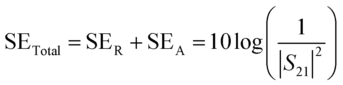
According to Schelkunoff theory, total EMI shielding effectiveness (SETotal) on the decibel scale can be described in the sum of reflection loss (SER), absorption loss (SEA), and multiple reflection loss (SEM). Further, SER as a primary EMI shielding mechanism for conductive materials can be quantified via the Fresnel's equation:8
| | | SET (dB) = SER + SEA + SEM | (1) |
| | 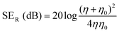 | (2) |
where
η and
η0 are the characteristic impedance of the shielding medium and air, respectively. In the transmission line theory, characteristic impedance
η is defined as follows:
9| |  | (3) |
where
μ,
σ, and
ε are the permeability, conductivity, and permittivity, respectively, and
ω = 2π
f is the angular frequency of the incident electromagnetic waves. Therefore, good conductors such as metal blocks and metal meshes are generally chosen for traditional EMI shielding due to their high reflection loss. However, the intrinsic physical characteristics including high density, brittleness, and poor flexibility co-constrain their applications in portable devices and new generation flexible or wearable electronics.
10
Novel structural design is one of the effective ways to optimize the EMI shielding properties of materials. Dense packing is no longer considered to be an effective strategy for EMI shielding because the shielding ability can be greatly improved by introducing additional interfaces within the medium.11 Increasing interfaces with mismatching impedance characteristics can contribute to additional internal scattering, also referred to as internal multiple scattering, and consequently, enhance absorption loss.12 In recent years, layer structural materials have attracted increasing attention in many fields due to their special physicochemical properties (anisotropic binding force, interlayer electron transport path, large specific surface area, etc.). A new family of two-dimensional transition metal carbides and nitrides referred to as MXenes is one of the research hotspots in electromagnetism, materials science, chemistry, etc.,13,14 due to their special microscopic layered structure and unique physicochemical properties.15 For example, a high EMI shielding effectiveness (EMI SE) of Ti3C2Tx synthesized by etching Ti3AlC2 in an acidic etchant has been reported by Y. Gogotsi et al., offering an SETotal value of about 85.0 dB in the X-band frequency range (8.2 to 12.4 GHz).16 Such an impressive EMI shielding property for Ti3C2Tx is mainly due to the enhanced internal scattering effect that comes from its multilayered structure. However, it is prone to self-accumulation into a compact structure due to the aggregation effect during mass manufacturing or the process of being used, which seriously affects its intrinsic characteristics.17 In addition, free-standing MXene-based materials like Ti3C2Tx thin films, in most situations, show suboptimal mechanical strength (brittleness). This deficiency puts them at risk for damage during long-term storage, transport, and some kinds of post-assembly processes such as bending, rolling, and folding.18,19 Therefore, a lightweight, large-scale, flexible, stable, and morphologically controllable structural reinforcement substrate is highly desired to support the MXene functional material's further use in portable and flexible EMI shielding.20–22
Macro-scale internal multiple scattering is also an important factor affecting the total electromagnetic wave loss. In order to make the most of this characteristic, researchers have developed macro-porous and multilayered conductive materials for high-performance EMI shielding; for example, porous graphene foams,23 flexible waterborne polyurethane (WPU)/silver nanowire (AgNW) nanocomposites with unidirectionally aligned micrometer-sized pores,24 and graphene-hybridized CuNW (CuNW@G) core–shell aerogels.25 Although all these materials show good EMI SE, their practical application remains challenging due to the following. (i) Weak in mass-production. The manufacturing processes of those macro-porous or multiple-layer materials often require stringent conditions, e.g., foaming, freeze-drying, or high-temperature calcination, which severely limit their continuous manufacturing and large-scale application.26,27 (ii) Lack of superior flexibility. Their mechanical properties tend to be rigid, due to Young's modulus being too high to meet the requirements of various curved surface application scenarios. (iii) Low utilization of functional materials.28,29
In this work, we propose a time-difference blow-spinning technology to continuously fabricate the multilayer polyacrylonitrile (MLPAN) nanofiber film with adjustable thickness and layer number in one step. By further conducting modifications with the as-prepared Ti3C2Tx solution via dip-coating, an ultralight and flexible hybrid fabric (named Ti3C2Tx/MLPAN) was obtained. It contained a multilayer nanofiber-network primary structure from MLPAN and a secondary nanoscale multilayer structure from Ti3C2Tx, verified via a series of micromorphological characterization methods. The hybrid fabric exhibited a low density of 639.0 mg cm−3 and good electrical properties including 23327.40 S m−1 of conductivity and 0.39 Ω sq−1 of sheet resistance. Due to its special dual-scale multilayer structure, the hybrid fabric exhibited a high EMI SETotal of up to 61.8 dB and a superior special EMI SE (thickness normalized SE, SSE/d) of 8535.9 dB cm2 g−1, which was considered the synergistic EMI shielding effect of multiple reflections and internal scattering. Moreover, benefits from the inherent mechanical advantages of the nanofiber substrate, Ti3C2Tx/MLPAN exhibited remarkable flexibility, illuminating only a slight change in the EMI SE after 5000 cycles of bending. The synergistic effects of internal reflection, internal multiple scattering and multiple reflections from dual-scale multilayer EMI shielding materials provide the possibility of applying the structurally designed advanced fabric in large-scale, portable, flexible and curved-surface EMI shielding and electromagnetic protection.
Results and discussion
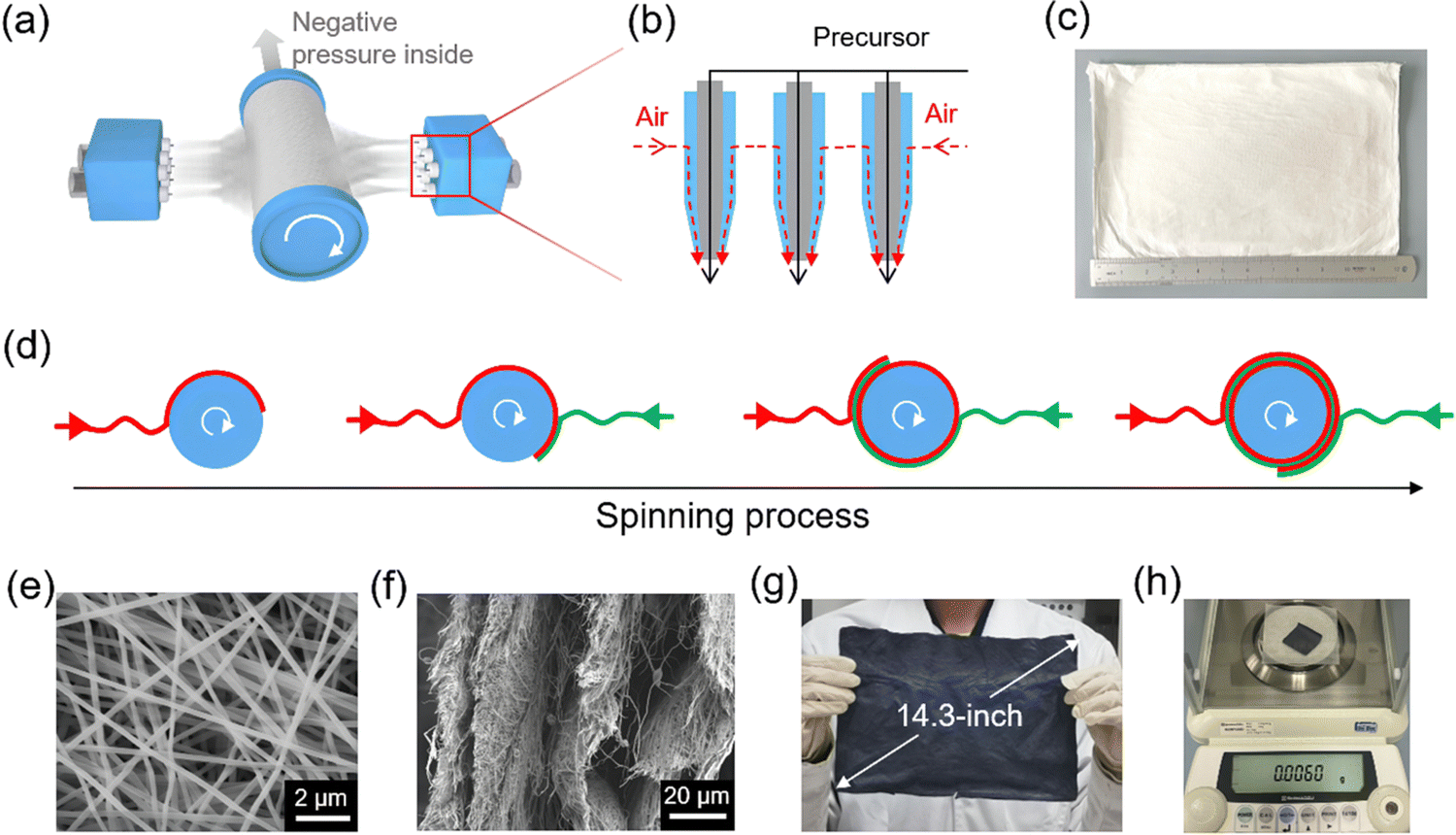
We designed and proposed a time-difference blow-spinning technology to directly separate the deposited nanofibers in both space and time, aiming to manufacture a morphologically adjustable multilayer fiber film in one step. The time-difference blow-spinning contains two main components, namely, a spinning module including two aspectant jets with staggered turn-on times, and a rotating speed-controlled porous cylinder as the fiber collector (Fig. 1a). The internal pressure of the collector was adjusted to negative by an air pump to assist fiber deposition. During the blow-spinning process, compressed air drives the precursor solution with a certain viscosity to form a high-speed jet (Fig. 1b and Fig. S1, ESI†). After solvent volatilization, the precursor fiber was obtained (Fig. 1c). In this method, the size of the product fiber mainly depends on the shape and surface area of the collector. Therefore, in order to scale up the product fiber size, the collector can be further designed on a large scale as a conveyor belt. Fig. 1d shows a typical time-difference blow-spinning process, wherein, the primary and the secondary spinning modules (red and green, respectively) turn on in sequence with a time difference while the collector rotated by 180 degrees. The thickness of the fiber film can be adjusted by controlling the solution injection speed, the airflow speed and the rotating speed of the cylindrical collector. Particularly, the rotating speed of the collector was set as 2 degrees per second in this work. As the rotating number increases, different layers of fiber can be obtained. In this work, a typical four-layer PAN fiber film with a network surface structure was fabricated as the substrate material (primary multilayer structure) for further EMI shielding application (Fig. 1e, f and Fig. S2, ESI†). The secondary multilayer structure material, Ti3C2Tx, was made by etching Ti3AlC2 using HCl/LiF etchant (Fig. S3, ESI†). In this process, Al layers were selectively etched after 24 h of continuous stirring. Previous studies illuminated that a certain amount of PVB can enhance the mechanical stability of a material, therefore, 0.1 wt% PVB was employed in this work to form a dip-coating precursor solution.11 By a subsequent facile dip-coating process, the Ti3C2Tx/MLPAN hybrid fabric with specific dimensions can be obtained (Fig. S4 and S5, ESI†). Such a dip-coating method is easy to scale up for industrial production (Fig. 1g). Benefiting from the multilayer structure and spatial network structure of MLPAN, the hybrid fabric exhibited an ultralow density, which is highly desired in modern portable and flexible electronics (Fig. 1h).
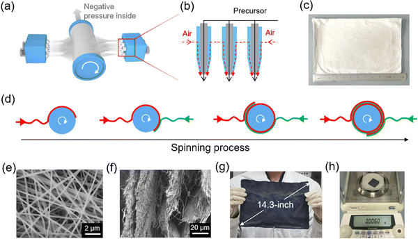 |
| | Fig. 1 The time-difference blow-spinning production. (a) Schematic of the spinning module and fiber collector. (b) Details of the airflow and precursor flow paths on spinning needles. (c) Photograph of a 14.3-inch (A4 scale) MLPAN. (d) Working diagram of the primary (red), secondary (green) spinning modules, and the rotating collector during time-difference blow-spinning. (e) Surface and (f) cross-sectional SEM images of the four-layer MLPAN. (g) Photograph of an A4-scale Ti3C2Tx/MLPAN, (h) and its ultralow density demonstration. | |
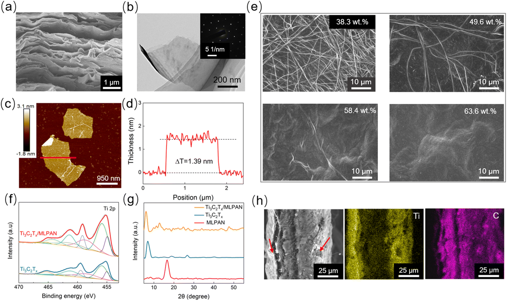
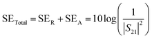
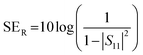
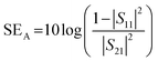
After etching the Al layers, the obtained Ti3C2Tx presented a layered accordion-like structure (Fig. 2a). The transmission electron microscope (TEM) image exhibited a two-dimensional nanosheet structure of few-layered Ti3C2Tx (Fig. 2b). The high-resolution TEM (HRTEM) showed an ∼0.26 nm lattice spacing, corresponding to the (![[1 with combining macron]](https://www.rsc.org/images/entities/char_0031_0304.gif) 010) lattice plane, which is consistent with that of the parent MAX phase (Fig. S6, ESI†).30 The selected area electron diffraction (SAED) exhibits a typical sixfold symmetric diffraction pattern, indicating the high crystallinity of the as-prepared Ti3C2Tx (Fig. 2b, inset). The thickness of the monolayer Ti3C2Tx was verified by atomic force microscopy (AFM) as ∼1.39 nm (Fig. 2c and d). The fine-adjusting of the mass ratio of Ti3C2Tx during the dip-coating process led to a series of Ti3C2Tx/MLPAN hybrid fabrics with different surface microstructures. As shown in Fig. 2e, the mesh structures of the MLPAN nanofiber substrates were gradually filled and covered with the increase in the mass radio of Ti3C2Tx, which was further proved by X-ray photoelectron spectroscopy (XPS) results (Fig. 2f and Fig. S7, ESI†). As the mass percentage of Ti3C2Tx reached 63.6 wt%, the surface of Ti3C2Tx/MLPAN became uniform (Fig. S8, ESI†). After dip-coating, Ti3C2Tx/MLPAN exhibited strong diffraction peaks in the X-ray diffraction (XRD) spectrum at 2θ of about 7 degrees (Fig. 2g), which corresponds to the (002) lattice plane of Ti3C2Tx, indicating that the crystal structure of Ti3C2Tx remained unchanged. In addition, the slight shift of the (002) lattice plane peak position of the hybrid fabric can be attributed to the interlayer spacing variation of Ti3C2Tx after dip-coating.31 The cross-section SEM image and corresponding energy dispersive spectroscopy (EDS, element mapping) of Ti3C2Tx/MLPAN illuminated the rich deposition of Ti3C2Tx on both sides of the fiber substrate, owing to the filtering effect from the surface network structure of blow-spun MLPAN nanofiber film (Fig. 2h and Fig. S9, ESI†). However, there was also a certain amount of Ti3C2Tx nanosheets inside the MLPAN, forming a secondary multilayer structure on each layer of PAN fiber (Fig. S10, ESI†). During thermogravimetric analysis (TGA) testing, a mass decrement was observed around 317 °C, representing the removal of water molecules and other functional groups (such as –OH and
010) lattice plane, which is consistent with that of the parent MAX phase (Fig. S6, ESI†).30 The selected area electron diffraction (SAED) exhibits a typical sixfold symmetric diffraction pattern, indicating the high crystallinity of the as-prepared Ti3C2Tx (Fig. 2b, inset). The thickness of the monolayer Ti3C2Tx was verified by atomic force microscopy (AFM) as ∼1.39 nm (Fig. 2c and d). The fine-adjusting of the mass ratio of Ti3C2Tx during the dip-coating process led to a series of Ti3C2Tx/MLPAN hybrid fabrics with different surface microstructures. As shown in Fig. 2e, the mesh structures of the MLPAN nanofiber substrates were gradually filled and covered with the increase in the mass radio of Ti3C2Tx, which was further proved by X-ray photoelectron spectroscopy (XPS) results (Fig. 2f and Fig. S7, ESI†). As the mass percentage of Ti3C2Tx reached 63.6 wt%, the surface of Ti3C2Tx/MLPAN became uniform (Fig. S8, ESI†). After dip-coating, Ti3C2Tx/MLPAN exhibited strong diffraction peaks in the X-ray diffraction (XRD) spectrum at 2θ of about 7 degrees (Fig. 2g), which corresponds to the (002) lattice plane of Ti3C2Tx, indicating that the crystal structure of Ti3C2Tx remained unchanged. In addition, the slight shift of the (002) lattice plane peak position of the hybrid fabric can be attributed to the interlayer spacing variation of Ti3C2Tx after dip-coating.31 The cross-section SEM image and corresponding energy dispersive spectroscopy (EDS, element mapping) of Ti3C2Tx/MLPAN illuminated the rich deposition of Ti3C2Tx on both sides of the fiber substrate, owing to the filtering effect from the surface network structure of blow-spun MLPAN nanofiber film (Fig. 2h and Fig. S9, ESI†). However, there was also a certain amount of Ti3C2Tx nanosheets inside the MLPAN, forming a secondary multilayer structure on each layer of PAN fiber (Fig. S10, ESI†). During thermogravimetric analysis (TGA) testing, a mass decrement was observed around 317 °C, representing the removal of water molecules and other functional groups (such as –OH and ![[double bond, length as m-dash]](https://www.rsc.org/images/entities/char_e001.gif) O) in Ti3C2Tx. As the temperature increased over 320 °C, the MLPAN started to thermally decompose and Ti3C2Tx was slightly affected (Fig. S11, ESI†), indicating the high thermal stability of Ti3C2Tx/MLPAN below 317 °C.
O) in Ti3C2Tx. As the temperature increased over 320 °C, the MLPAN started to thermally decompose and Ti3C2Tx was slightly affected (Fig. S11, ESI†), indicating the high thermal stability of Ti3C2Tx/MLPAN below 317 °C.
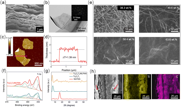 |
| | Fig. 2 Micromorphological, crystallographic, and chemical characteristics. (a) Cross-section SEM image of multilayer Ti3C2Tx. (b) TEM image of the Ti3C2Tx nanosheet, the inset shows the corresponding SAED pattern. (c) AFM image of the Ti3C2Tx nanosheet after a five-minute ultrasonic dispersion, (d) and its thickness measurement. (e) Surface SEM images of Ti3C2Tx/MLPAN with different Ti3C2Tx contents of 38.3 wt%, 49.6 wt%, 58.4 wt% and 63.6 wt%. (f) XPS peak differentiation imitating the analysis of Ti 2p. (g) XRD spectra of MLPAN, Ti3C2Tx, and Ti3C2Tx/MLPAN. (h) Cross-sectional SEM image, and EDS element mapping of Ti and C. | |
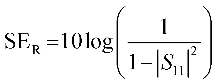
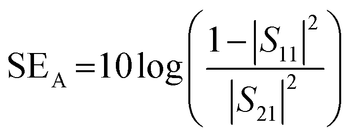
The electrical properties, including conductivity and sheet resistance, are the main parameters that affect a material's EMI shielding property. We first measured the electrical properties of Ti3C2Tx/MLPAN with different Ti3C2Tx contents of 38.3 wt%, 49.6 wt%, 58.4 wt% and 63.6 wt%. As the mass ratio of Ti3C2Tx increased to 63.6 wt%, the conductivity and sheet resistance of the hybrid fabric were 23327.40 S m−1 and 0.38 Ω sq−1, respectively (Fig. 3a). Such good electrical properties of the hybrid fabric mainly arise from the high electron density of states near the Fermi level [N(Ef)] of Ti3C2Tx.32 EMI SE is a key indicator of EMI shielding associated fields, which can be expressed using S-parameters:
| |  | (4) |
| |  | (5) |
| |  | (6) |
As shown in Fig. S12 (ESI
†), SE
A and SE
R of Ti
3C
2T
x/MLPAN with different Ti
3C
2T
x contents were calculated from
S11 and
S21. Ti
3C
2T
x/MLPAN enables efficient EMI shielding in the X-band with high EMI SE
Total. The SE
Total of the hybrid fabric reached ∼61.8 dB as the mass ratio of Ti
3C
2T
x increased to 63.6 wt% (
Fig. 3b), wherein SE
A reached ∼56.7 dB and SE
R reached ∼5.1 dB (
Fig. 3c and Fig. S13, ESI
†). This result indicates an ultrahigh shielding efficiency of over 99.9999%, enabling an almost complete blocking of the incident electromagnetic waves (
Fig. 3d). Compared with the EMI SE obtained when the same mass of Ti
3C
2T
x was filtered into the membrane alone (Fig. S14, ESI
†), the SE
Total of Ti
3C
2T
x/MLPAN increased by 35.8%. Fig. S15 (ESI
†) shows that the EMI SE of MLPAN was almost zero. The type of EMI shielding can be determined by the power coefficients, including the reflection coefficient (
R), absorption coefficient (
A), and transmission coefficient (
T).
8 As shown in Table S1 (ESI
†), the low
A and low
R of MLPAN led to an extremely low EMI shielding performance (
T = 0.988). The results indicate that MLPAN is electromagnetically insensitive and only acts as a flexible multilayer substrate to separate Ti
3C
2T
x at the first scale (20 μm). On the other hand, the
A value of Ti
3C
2T
x/MLPAN (63.6 wt%) reached 0.318, which is 75.7% higher than that of the Ti
3C
2T
x film with the same Ti
3C
2T
x mass (
A = 0.181). This result can be attributed to the enhanced EM wave absorption for Ti
3C
2T
x/MLPAN caused by the dual-scale multilayer structure that increases both internal scattering and multiple reflections. As a proof-of-concept, a normal printing paper (
Fig. 3e, left) and a Ti
3C
2T
x/MLPAN hybrid fabric (
Fig. 3e, right) were placed successively between a wireless charging pad and a smartphone. As shown in
Fig. 3e, the normal printing paper did not affect the wireless charging process. On the contrary, the wireless charging was successfully interrupted by the Ti
3C
2T
x/MLPAN hybrid fabric, indicating the great EMI shielding property of the latter. Flexibility and mechanical stability are two other important factors for cambered and deformable devices. We used Ti
3C
2T
x/MLPAN as a conducting wire to light an LED in different forms to visually verify its flexibility. As shown in
Fig. 3f, the LED was always on, even when the Ti
3C
2T
x/MLPAN was knotted and winding, indicating the shape-independent electrical conductivity of the hybrid fabric. In terms of micromorphology, Ti
3C
2T
x/MLPAN showed no cracks or creases after folding and coiling (
Fig. 3g and Fig. S16, S17, ESI
†), mainly due to the nano-size effect of one-dimensional PAN fibers. Cyclic bending experiments were further performed on Ti
3C
2T
x/MLPAN with different Ti
3C
2T
x contents of 38.3 wt%, 49.6 wt%, 58.4 wt% and 63.6 wt%. The results only showed a slight change in the resistances of those samples after 1000-cycle bending (
Fig. 3h). Real-time resistance changes of the samples were also recorded
via a computer-controlled electrochemical workstation as shown in Fig. S18 (ESI
†); the results indicated a steady variation trend and low loss of conductivity. To further demonstrate the microstructure stability, we collected SEM images of Ti
3C
2T
x/MLPAN with different Ti
3C
2T
x contents of 38.3 wt%, 49.6 wt%, 58.4 wt% and 63.6 wt% before and after 1000-cycle bending (Fig. S19, ESI
†). By comparing the SEM images before and after bending, it was found that the microstructure of Ti
3C
2T
x/MLPAN remained almost the same, indicating a high mechanical stability of Ti
3C
2T
x/MLPAN under deformation conditions. Moreover, Ti
3C
2T
x/MLPAN retained ∼93% of its initial EMI SE after over 5000 cycles of bending, indicating both remarkable flexibility and outstanding mechanical stability (
Fig. 3i). A 24 hour soaking experiment was further performed to prove the waterproof property of Ti
3C
2T
x/MLPAN. As shown in Fig. S20 (ESI
†), the average resistance of the sample before and after soaking remained broadly unchanged, indicating the high stability of Ti
3C
2T
x/MLPAN in water. A comprehensive consideration of thickness, density, usability, flexibility, mechanical stability and EMI shielding property indicated that the Ti
3C
2T
x/MLPAN hybrid fabric is comparable with, and even better than, most reported EMI shielding films and bulk materials (
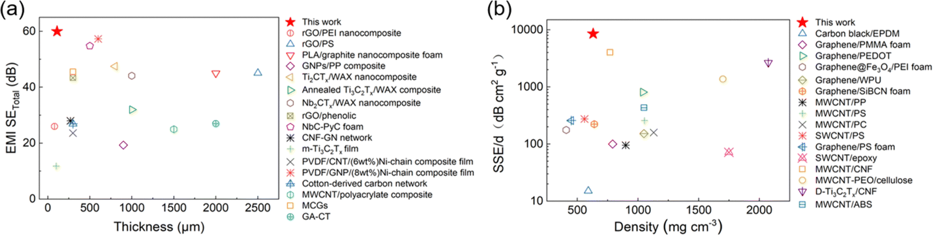
Fig. 4).
33–63 Detailed data for the comparison of EMI shielding properties including SE
Total and thickness-normalized specific SE (SSE/d) are shown in
Tables 1 and 2.
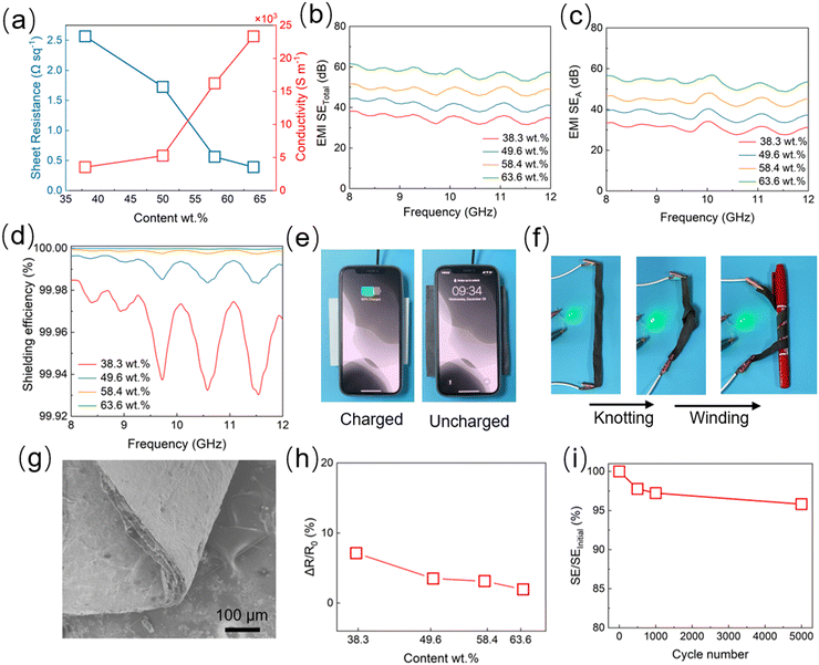 |
| | Fig. 3 Electrical, electromagnetic and mechanical properties. (a) Sheet resistance and conductivity of Ti3C2Tx/MLPAN with Ti3C2Tx content of 38.3 wt%, 49.6 wt%, 58.4 wt% and 63.6 wt%. (b) EMI SETotal, (c) EMI SEA, and shielding efficiency (%) of Ti3C2Tx/MLPAN with different Ti3C2Tx contents. (e) A proof-of-concept of the wireless charging blocking with Ti3C2Tx/MLPAN (right) and a printing paper control group. (f) An intuitionistic exhibition of the mechanical properties of Ti3C2Tx/MLPAN as it is knotting and winding. (g) SEM image of Ti3C2Tx/MLPAN in the bending state. (h) The rate of resistance change of Ti3C2Tx/MLPAN with different Ti3C2Tx contents of 38.3 wt%, 49.6 wt%, 58.4 wt% and 63.6 wt% after 1000 cycles of bending. (i) Changes in EMI SE for Ti3C2Tx/MLPAN after 500, 1000, and 5000 cycles of bending. | |
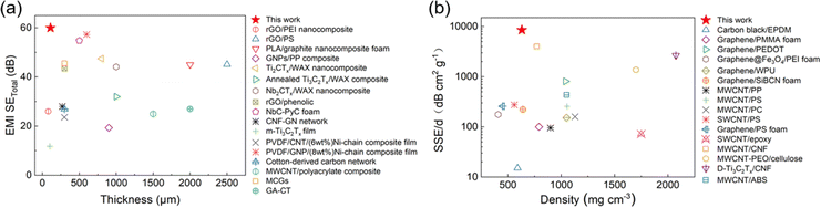 |
| | Fig. 4 Comparison of the EMI shielding performance. (a) EMI SETotalversus the thickness of Ti3C2Tx/MLPAN and other EMI shielding materials from the references. (b) Thickness-normalized specific SE (SSE/d) of Ti3C2Tx/MLPAN with a density of 639.0 mg cm−3 and other EMI shielding materials from the references. | |
Table 1 Fill rate, SETotal and thickness of Ti3C2Tx/MLPAN and other EMI shielding materials
| Materials |
Fill rate [wt%] |
SETotal [dB] |
Thickness [mm] |
Ref. |
| Ti3C2Tx/MLPAN |
63.6 |
61.8 |
0.11 |
This work |
| MWCNT/polyacrylate composites |
10 |
25 |
1.5 |
33
|
| rGo/PEI nanocomposites |
2.5 |
26 |
0.08 |
34
|
| rGo/ps |
7 |
45.1 |
2.5 |
35
|
| PLA/graphite nanocomposite foam |
2.5 |
45 |
2 |
36
|
| GNPs/PP composites |
10 |
19.3 |
0.9 |
37
|
| Ti2CTx/WAX |
80 |
47.5 |
0.8 |
38
|
| Annealed Ti3C2Tx/WAX composite |
90 |
32 |
1 |
39
|
| Nb2CTx/WAX nanocomposites |
80 |
44.09 |
1 |
40
|
| rGo/phenolic |
70 |
43.4 |
0.3 |
41
|
| NbC-PyC foam |
37.2 |
54.8 |
0.5 |
42
|
| CNF−GN networks |
17.2 (GN) |
28 |
0.27 |
43
|
| m-Ti3C2Tx film |
15 |
11.8 |
0.1 |
44
|
| PVDF/CNT/6 wt% Ni-chain composite films |
6 |
23.6 |
0.3 |
45
|
| PVDF/GNP/8 wt% Ni-chain composite films |
8 |
57.3 |
0.6 |
45
|
| Cotton-derived carbon network |
— |
26.9 |
0.3 |
46
|
| MCGs |
— |
45.5 |
0.3 |
47
|
| GA-CT |
— |
27 |
2 |
48
|
Table 2 Fill rate, density, SETotal and thickness-normalized specific SE (SSE/d) of Ti3C2Tx/MLPAN and other EMI shielding materials
| Materials |
Fill rate [wt%] |
Density [mg cm−3] |
SETotal [dB] |
SSE/d [dB cm2 g−1] |
Ref. |
| Ti3C2Tx/MLPAN |
63.6 |
639.0 |
61.8 |
8535.9 |
This work |
| MWCNT/ABS |
15 |
1050.4 |
50 |
432.7 |
49
|
| Carbon black/EPDM |
— |
590 |
— |
15.1 |
50
|
| Graphene/PMMA foam |
5 |
791.6 |
19 |
100 |
51
|
| Graphene/PEDOT |
25 |
1040 |
70 |
814 |
52
|
| Graphene@Fe3O4/PEI foam |
10 |
409 |
18.2 |
176 |
53
|
| Graphene/WPU |
7.7 |
1049.18 |
32 |
152.5 |
54
|
| Graphene/SiBCN foam |
0.5 |
640 |
18.56 |
223 |
55
|
| MWCNT/PP |
5 (vol%) |
898.88 |
24 |
95.4 |
56
|
| MWCNT/PS |
20 |
1052.6 |
60 |
285 |
57
|
| MWCNT/PC |
20 |
1130 |
39 |
159.7 |
58
|
| SWCNT/PS |
7 |
560 |
18.56 |
275 |
59
|
| Graphene/ps foam |
30 |
450.3 |
29 |
257.6 |
60
|
| SWCNT/epoxy |
15 |
1748.25 |
25 |
71.5 |
3
|
| MWCNT/CNF |
75 |
770 |
46.4 |
4017.3 |
61
|
| MWCNT-PEO/cellulose |
40 |
1700 |
35 |
1372 |
62
|
| D-Ti3C2Tx/CNF |
80 |
2073.95 |
25.8 |
2647 |
63
|
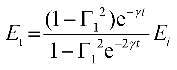
The dual-scale multilayer structure of Ti3C2Tx/MLPAN leads to enhanced electromagnetic wave dissipation via internal reflection, multiple scattering and multiple reflections (Fig. 5a). When the incident electromagnetic wave reaches the first layer of Ti3C2Tx, partial energy is immediately reflected and the rest passes through Ti3C2Tx. The same process happens when the transmitted wave reaches the next layer of Ti3C2Tx, until it passes through one layer of the PAN substrate. A similar process occurs when the electromagnetic wave reaches the next layer of the PAN substrate, during which, both internal scattering and multiple reflections are significantly increased, resulting in a higher A value. This result proves that such a dual-scale multilayer structure of Ti3C2Tx/MLPAN contributes to the effective attenuation and elimination of EM waves.64 It is generally considered that the multiple reflections inside a conducting medium occur only when the material's thickness is lower than the corresponding skin depth. The skin depth of Ti3C2Tx was calculated as 154.6 μm, which is much bigger than the thickness of monolayer Ti3C2Tx (1.39 nm), leading to the multiple reflections occurring in Ti3C2Tx (Fig. 5b). For each layer of Ti3C2Tx, the total transmitted wave is the sum of all the partial waves (Fig. 5b, green arrows) transmitted past the Z2–Z1 interface:65
| | 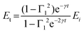 | (7) |
where
Et is the total transmission wave,
Ei is the incident wave,
Γ1 is the reflection coefficient,
γ is the propagation constant, and
t is the thickness of the conducting medium. The total transmission wave for a medium with
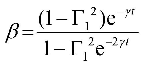
N layers (
EtN) can be described as follows:
| | 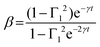 | (9) |
It was observed that the intensity of the incident electromagnetic wave exponentially decreases by attenuation coefficient
β as the layer number increases. This is mainly due to the impedance mismatch between free space and the conducting medium. Therefore, adequate surface exposure for conducting materials can be considered as an effective method to improve EMI shielding properties.
 |
| | Fig. 5 Principle and electromagnetic simulations. (a) Schematic of the EMI shielding principle of the dual-scale multilayer Ti3C2Tx/MLPAN hybrid fabric. (b) Multiple reflections occurred inside monolayer Ti3C2Tx when the material thickness was lower than the corresponding skin depth, where γ is the propagation constant and t is the thickness of the material. Simulation results of (c) SETotal, and the corresponding S-parameters include (d) |S11| and (e) |S21|. Field distribution simulation results for electromagnetic waves including the (f) electric field and (g) magnetic field. | |
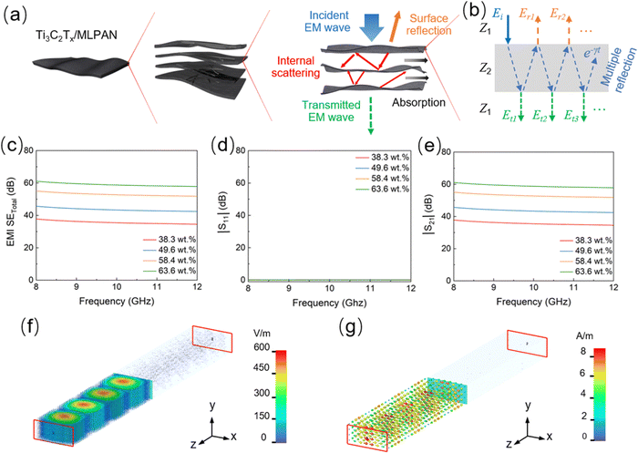
We further performed time domain simulation to verify the EMI shielding principle of Ti3C2Tx/MLPAN and the electromagnetic field behavior during the penetration of plane electromagnetic waves via the computer simulation technology microwave studio (CST MWS 2019) software. A four-layer sandwich structure approximate model (Fig. S21, ESI†) was used to simulate as-prepared Ti3C2Tx/MLPAN (details in ESI†). Particularly, the conductivity of the external Ti3C2Tx was set to be different from the internal one because the coating densities of Ti3C2Tx were different as mentioned before. Simulation results showed conductivity-dependent properties including high |S21|, low |S11|, as well as SETotal from 38.2 dB to 61.8 dB, which are consistent with the test results from VNA (Fig. 5c–e). The field distribution simulation of electromagnetic waves including electric and magnetic fields was also performed. It was found that the electric field intensity rapidly attenuated to ∼0.07% of its initial value as it passed through Ti3C2Tx/MLPAN (Fig. 5f and Fig. S22, ESI†), which agrees well with experimental data. A similar situation was also found in the magnetic field distribution results (Fig. 5g and Fig. S23, ESI†), which corroborated the test results from VNA and illuminated the application potential for the flexible and dual-scale multilayer Ti3C2Tx/PAN fabric in EMI shielding and electromagnetic protection.
Conclusions
In this work, we have proposed a time-difference blow-spinning technology and fabricated an MLPAN nanofiber substrate in one step. By further conducting modification with the as-prepared MXene (Ti3C2Tx) solution via dip-coating, an ultralight and flexible hybrid fabric (Ti3C2Tx/MLPAN) was obtained. The primary multilayer nanofiber-network structure from MLPAN and a secondary nanoscale multilayer structure from Ti3C2Tx were verified via a series of micromorphological characterization methods. Due to the network structure of the PAN fiber, the density of Ti3C2Tx/MLPAN was measured to be as low as 639.0 mg cm−3. By coating with a highly conductive MXene, Ti3C2Tx/MLPAN exhibited good electrical properties including a conductivity of 23327.40 S m−1 and sheet resistance of 0.39 Ω sq−1. By VNA testing, the hybrid fabric exhibited a high EMI SE up to 61.8 dB and a superior SSE/d of 8535.9 dB cm2 g−1, which is considered the synergistic EMI shielding effect of multiple reflections and internal scattering. Moreover, Ti3C2Tx/MLPAN showed both remarkable flexibility and mechanical stability, enabling it to be bent for five thousand cycles. This work developed a mass-production strategy for morphologically adjustable multilayer nanofibers and provided the possibility of applying structurally designed advanced fabric in large-scale, portable, flexible and curved-surface EMI shielding and electromagnetic protection.
Experimental
Materials
Polyacrylonitrile (PAN, Mw = 150![[thin space (1/6-em)]](https://www.rsc.org/images/entities/char_2009.gif) 000), dimethyl sulfoxide (DMSO, 99.8%), TiH2 (400 mesh, 99%), Al (5–6 μm, 99.8%), and TiC (400 mesh, 98%) were purchased from Shanghai Aladdin Bio-Chem Technology Co. Ltd. Fluorocarbon surfactant (FS-3100) was purchased from DuPont Research & Development and Management Co. Ltd. All reagents were used without further purification.
000), dimethyl sulfoxide (DMSO, 99.8%), TiH2 (400 mesh, 99%), Al (5–6 μm, 99.8%), and TiC (400 mesh, 98%) were purchased from Shanghai Aladdin Bio-Chem Technology Co. Ltd. Fluorocarbon surfactant (FS-3100) was purchased from DuPont Research & Development and Management Co. Ltd. All reagents were used without further purification.
Fabrication of PAN fiber substrates
First, 0.14 g of PAN (Mw = 150000) was dispersed in 100.00 g of DMSO and stirred for 2 h at 70 °C. Then, 30–50 μL of FS-3100 can be selected to add to the precursor solution depending on the actual ambient temperature and humidity. To perform time-difference blow-spinning, the solution was injected into two integrated blow-spinning apparatus with a liquid-gas two-channel six-needle module and a rotating fiber collector. The internal pressure of the collector was adjusted to negative by an air pump to assist fiber deposition. During blow spinning, the airflow velocity was set to 4.5 m3 h−1, and the injection speed of the solution was kept at a value of 2.0 mL h−1.
Synthesis of Ti3AlC2 powder
Ti3AlC2 was synthesized as described in our previous work.30 Typically, TiH2, Al, and TiC powders were mixed in a 1:1.2:2 mole ratio, followed by ball-milling for 18 h. The mixture was then sintered in a tube oven at 1450 °C for 2 h in a flowing Ar atmosphere. On crushing and sieving the resulting compact powder, Ti3AlC2 powder with a size of <38 μm was obtained.
Preparation of Ti3C2Tx suspension
The few-layer Ti3C2Tx suspension was synthesized by etching the Ti3AlC2 MAX phase in LiF/HCl hybrid etchant according to the previously reported route.16 Typically, a total of 3.0 g of Ti3AlC2 powder was gradually added (over the course of 3 min) to the LiF (4.8 g)/HCl (60 mL, 9 M) mixture. Then, the mixture was left under continuous stirring at room temperature for 24 h. Afterward, the resultant acidic mixture was washed repeatedly with deionized water via centrifugation at 3500 rpm for 5 min per cycle until the pH of the supernatant reached 6. The stable dark-green supernatant was collected to obtain the few-layer Ti3C2Tx suspension with a concentration of ∼2.0 × 10⁻³ g mL−1, which was determined by filtering a known volume of the suspension and measuring the weight of the film after vacuum drying.
Preparation of Ti3C2Tx/MLPAN films
In a typical dip-coating process, the as-prepared MLPAN was immersed in the solution of the coating material (Ti3C2Tx) at a constant speed. PVB/ethanol was mixed into the Ti3C2Tx aqueous solution, forming a 0.1 wt% PVB precursor solution for dip-coating. The Ti3C2Tx thin layer was deposited on the MLPAN substrate and the solvent evaporated from the liquid while the substrate was pulled up, forming the Ti3C2Tx/MLPAN hybrid fabric.
Dip coating processing.
The rolling dip coating equipment consisted of three parts: one transmission shaft (radius = 2 cm), four squeezing shafts (radius = 1 cm, wheel base is adjustable), and one electrically driven collecting shaft (radius = 2 cm). Particularly, the squeezing shafts inside the precursor solution can help to eliminate the air inside the MLPAN; the squeezing shafts outside the precursor solution were used to extrude the excess solvent to accelerate the evaporation and forming process.
Materials characterization
X-ray powder diffraction data were collected using an XRD diffractometer (D/max 2500, Rigaku, Japan) in Cu Kα radiation (λ = 1.54178 Å). The micromorphological analysis was performed by means of a field emission scanning electron microscope (FE-SEM, LEO-1530, Zeiss, Germany) with an EDS attachment module and a transmission electron microscope (TEM, JEM-F200_TFEG, JEOL, Japan). The thickness of the as-prepared sample was measured by an atomic force microscope (AFM, Dimension ICON, Bruker, Germany). Thermogravimetric analysis (TGA) was performed using a thermogravimetric analyzer (STA 449 F3, Jupiter, Germany). The electrical properties of the as-prepared samples were examined on an IV/CV probe installation (PRECISION SYSTEMS INDUSTRIAL LIMITED, HK, China), including an EPS4 probe station, a PCA1000 LCR instrument, and PPTS-CV IV/CV test software. The IV/CV probe test system was linked to an electrochemical workstation (Metrohm Multi Autlab M204, Switzerland) for accurate data recording.
Author contributions
Wei Song: Validation, methodology, writing – original draft, formal analysis. Shuang Hu: writing – review & editing. Jiaxiang Lu: writing – review & editing. Liang Su: writing – review & editing. Zhemin Li: writing – review & editing. Junchen Liu: formal analysis. Yufeng Wu: formal analysis. Jianan Song: writing – review & editing. Zhenglian Liu: writing – review & editing. Shuaikai Xu: conceptualization, writing – review & editing, project administration, funding acquisition. Sen Lin: conceptualization, validation, writing – review & editing, project administration, funding acquisition.
Conflicts of interest
There are no conflicts to declare.
Acknowledgements
This study was supported by the National Natural Science Foundations of China (Grant 62104051), Natural Science Foundation of Guangxi Province (Grant No. 2021JJB160104, and 2020JJB120060), and the Special Talents Foundation of Guangxi Province (Grant No. 2021AC19174).
References
- X. Ye, B. Shi, M. Li, Q. Fan, X. Qi, X. Liu, S. Zhao, L. Jiang, X. Zhang, K. Fu, L. Qu and M. Tian, Nano Energy, 2022, 97, 107114 CrossRef CAS.
- B. Shi, Y. Shang, Y. Pei, S. Pei, L. Wang, D. Heider, Y. Y. Zhao, C. Zheng, B. Yang, S. Yarlagadda, T. W. Chou and K. K. Fu, Nano Lett., 2020, 20, 5504–5512 CrossRef CAS PubMed.
- Y. Huang, N. Li, Y. Ma, F. Du, F. Li, X. He, X. Lin, H. Gao and Y. Chen, Carbon, 2007, 45, 1614–1621 CrossRef CAS.
- O. Balci, E. O. Polat, N. Kakenov and C. Kocabas, Nat. Commun., 2015, 6, 6628 CrossRef CAS PubMed.
- S. R. Y. Sachiko, Ind. Health, 2017, 56, 96–105 Search PubMed.
- G. Redlarski, B. Lewczuk, A. Zak, A. Koncicki, M. Krawczuk, J. Piechocki, K. Jakubiuk, P. Tojza, J. Jaworski, D. Ambroziak, L. Skarbek and D. Gradolewski, BioMed Res. Int., 2015, 2015, 234098 Search PubMed.
- M. Zhang, M.-S. Cao, J.-C. Shu, W.-Q. Cao, L. Li and J. Yuan, Mater. Sci. Eng., R, 2021, 145, 100627 CrossRef.
-
S. A. Schelkunoff, D Van Nostrand, New York, 1943, pp. 303–312 Search PubMed.
- M. Peng and F. J. J. o A. P. Qin, J. Appl. Phys., 2021, 130, 225108 CrossRef CAS.
- G. Han, Z. Ma, B. Zhou, C. He, B. Wang, Y. Feng, J. Ma, L. Sun and C. Liu, J. Colloid Interface Sci., 2021, 583, 571–578 CrossRef CAS PubMed.
- S. Lin, J. Liu, Q. Wang, D. Zu, H. Wang, F. Wu, X. Bai, J. Song, Z. Liu, Z. Li, K. Huang, B. Li, M. Lei and H. Wu, Adv. Mater. Technol., 2019, 5, 1900761 CrossRef.
- M. Han, X. Yin, K. Hantanasirisakul, X. Li, A. Iqbal, C. B. Hatter, B. Anasori, C. M. Koo, T. Torita, Y. Soda, L. Zhang, L. Cheng and Y. Gogotsi, Adv. Opt. Mater., 2019, 7, 1900267 CrossRef.
- Q. Gao, Y. Pan, G. Zheng, C. Liu, C. Shen and X. Liu, Adv. Compos. Hybrid Mater., 2021, 4, 274–285 CrossRef CAS.
- H. Cheng, Y. Pan, X. Wang, C. Liu, C. Shen, D. W. Schubert, Z. Guo and X. Liu, Nanomicro Lett., 2022, 14, 63 CrossRef CAS PubMed.
- A. Iqbal, P. Sambyal and C. M. Koo, Adv. Funct. Mater., 2020, 30, 2000883 CrossRef CAS.
- F. S. K. H. Aamir Iqbal, K. Myung-Ki, K. Jisung, J. Hong and K. D. K. Y. Hyerim, Science, 2020, 369, 446–450 CrossRef PubMed.
- Y. Zhang, Y. Yan, H. Qiu, Z. Ma, K. Ruan and J. Gu, J. Mater. Sci. Technol., 2022, 103, 42–49 CrossRef.
- L.-X. Liu, W. Chen, H.-B. Zhang, Y. Zhang, P. Tang, D. Li, Z. Deng, L. Ye and Z.-Z. Yu, Chem. Eng. J., 2022, 430, 133074 CrossRef CAS.
- P. Tang, Z. Deng, Y. Zhang, L. X. Liu, Z. Wang, Z. Z. Yu and H. B. Zhang, Adv. Funct. Mater., 2022, 32, 2112156 CrossRef CAS.
- L. X. Liu, W. Chen, H. B. Zhang, Q. W. Wang, F. Guan and Z. Z. Yu, Adv. Funct. Mater., 2019, 29, 1905197 CrossRef CAS.
- D. Y. Li, L. X. Liu, Q. W. Wang, H. B. Zhang, W. Chen, G. Yin and Z. Z. Yu, ACS Appl. Mater. Interfaces, 2022, 14, 12703–12712 CrossRef CAS PubMed.
- L. X. Liu, W. Chen, H. B. Zhang, L. Ye, Z. Wang, Y. Zhang, P. Min and Z. Z. Yu, Nanomicro Lett., 2022, 14, 111 CrossRef CAS PubMed.
- B. Shen, Y. Li, D. Yi, W. Zhai, X. Wei and W. Zheng, Carbon, 2016, 102, 154–160 CrossRef CAS.
- Z. Zeng, M. Chen, Y. Pei, S. I. Seyed Shahabadi, B. Che, P. Wang and X. Lu, ACS Appl. Mater. Interfaces, 2017, 9, 32211–32219 CrossRef CAS PubMed.
- S. Wu, M. Zou, Z. Li, D. Chen, H. Zhang, Y. Yuan, Y. Pei and A. Cao, Small, 2018, 14, e1800634 CrossRef PubMed.
- P. Song, B. Liu, C. Liang, K. Ruan, H. Qiu, Z. Ma, Y. Guo and J. Gu, Nanomicro Lett., 2021, 13, 91 CAS.
- C. Liang, Z. Gu, Y. Zhang, Z. Ma, H. Qiu and J. Gu, Nanomicro Lett., 2021, 13, 181 CAS.
- J. Liu, S. Lin, K. Huang, C. Jia, Q. Wang, Z. Li, J. Song, Z. Liu, H. Wang, M. Lei and H. Wu, npj Flexible Electron., 2020, 4, 1–7 CrossRef CAS.
- C. L. H. S. K. J. E. O. A. E. J. Joo, Synth. Met., 1999, 102, 1346–1349 CrossRef.
- S. Xu, G. Wei, J. Li, W. Han and Y. Gogotsi, J. Mater. Chem. A, 2017, 5, 17442–17451 RSC.
- F. Shahzad, M. Alhabeb, C. B. Hatter, B. Anasori, S. Man Hong, C. M. Koo and Y. Gogotsi, Science, 2016, 353, 1137–1140 CrossRef CAS PubMed.
- M. Khazaei, M. Arai, T. Sasaki, C.-Y. Chung, N. S. Venkataramanan, M. Estili, Y. Sakka and Y. Kawazoe, Adv. Funct. Mater., 2013, 23, 2185–2192 CrossRef CAS.
- Y. Li, C. Chen, S. Zhang, Y. Ni and J. Huang, Appl. Surf. Sci., 2008, 254, 5766–5771 CrossRef CAS.
- P. Sawai, P. P. Chattopadhaya and S. Banerjee, Mater. Today: Proc., 2018, 5, 9989–9999 CAS.
- D.-X. Yan, H. Pang, B. Li, R. Vajtai, L. Xu, P.-G. Ren, J.-H. Wang and Z.-M. Li, Adv. Funct. Mater., 2015, 25, 559–566 CrossRef CAS.
- G. Wang, G. Zhao, S. Wang, L. Zhang and C. B. Park, J. Mater. Chem. C, 2018, 6, 6847–6859 RSC.
- F. E. Alam, J. Yu, D. Shen, W. Dai, H. Li, X. Zeng, Y. Yao, S. Du, N. Jiang and C. T. Lin, Polymers, 2017, 9, 662 CrossRef PubMed.
- X. Li, X. Yin, S. Liang, M. Li, L. Cheng and L. Zhang, Carbon, 2019, 146, 210–217 CrossRef CAS.
- M. Han, X. Yin, H. Wu, Z. Hou, C. Song, X. Li, L. Zhang and L. Cheng, ACS Appl. Mater. Interfaces, 2016, 8, 21011–21019 CrossRef CAS PubMed.
- K. Rajavel, X. Yu, P. Zhu, Y. Hu, R. Sun and C. Wong, J. Alloys Compd., 2021, 877, 160235 CrossRef CAS.
- A. P. Singh, P. Garg, F. Alam, K. Singh, R. B. Mathur, R. P. Tandon, A. Chandra and S. K. Dhawan, Carbon, 2012, 50, 3868–3875 CrossRef CAS.
- X. Liu, H. Liu, H. Xu, W. Xie, M. Li, J. Liu, G. Liu, A. Weidenkaff and R. Riedel, J. Colloid Interface Sci., 2022, 606, 1543–1553 CrossRef CAS PubMed.
- W. L. Song, J. Wang, L. Z. Fan, Y. Li, C. Y. Wang and M. S. Cao, ACS Appl. Mater. Interfaces, 2014, 6, 10516–10523 CrossRef CAS PubMed.
- B. Ji, S. Fan, S. Kou, X. Xia, J. Deng, L. Cheng and L. Zhang, Carbon, 2021, 181, 130–142 CrossRef CAS.
- B. Zhao, S. Wang, C. Zhao, R. Li, S. M. Hamidinejad, Y. Kazemi and C. B. Park, Carbon, 2018, 127, 469–478 CrossRef CAS.
- X. Ma, Y. Li, B. Shen, L. Zhang, Z. Chen, Y. Liu, W. Zhai and W. Zheng, ACS Appl. Mater. Interfaces, 2018, 10, 38255–38263 CrossRef CAS PubMed.
- Z. Chen, D. Yi, B. Shen, L. Zhang, X. Ma, Y. Pang, L. Liu, X. Wei and W. Zheng, Carbon, 2018, 139, 271–278 CrossRef CAS.
- W.-L. Song, X.-T. Guan, L.-Z. Fan, W.-Q. Cao, C.-Y. Wang and M.-S. Cao, Carbon, 2015, 93, 151–160 CrossRef CAS.
- M. H. Al-Saleh, W. H. Saadeh and U. Sundararaj, Carbon, 2013, 60, 146–156 CrossRef CAS.
- P. Ghosh and A. Chakrabarti, Eur. Polym. J., 2000, 36, 1043–1054 CrossRef CAS.
- H. B. Zhang, Q. Yan, W. G. Zheng, Z. He and Z. Z. Yu, ACS Appl. Mater. Interfaces, 2011, 3, 918–924 CrossRef CAS PubMed.
- N. Agnihotri, K. Chakrabarti and A. De, RSC Adv., 2015, 5, 43765–43771 RSC.
- B. Shen, W. Zhai, M. Tao, J. Ling and W. Zheng, ACS Appl. Mater. Interfaces, 2013, 5, 11383–11391 CrossRef CAS PubMed.
- S.-T. Hsiao, C.-C. M. Ma, H.-W. Tien, W.-H. Liao, Y.-S. Wang, S.-M. Li and Y.-C. Huang, Carbon, 2013, 60, 57–66 CrossRef CAS.
- C. Wang, Y. Liu, M. Zhao, F. Ye and L. Cheng, Ceram. Int., 2018, 44, 22830–22839 CrossRef CAS.
- M. H. Al-Saleh and U. Sundararaj, Carbon, 2009, 47, 1738–1746 CrossRef CAS.
- M. Arjmand, T. Apperley, M. Okoniewski and U. Sundararaj, Carbon, 2012, 50, 5126–5134 CrossRef CAS.
- S. Pande, A. Chaudhary, D. Patel, B. P. Singh and R. B. Mathur, RSC Adv., 2014, 4, 13839 RSC.
- Y. Yang, M. C. Gupta, K. L. Dudley and R. W. Lawrence, Nano Lett., 2005, 5, 2131–2134 CrossRef CAS PubMed.
- D.-X. Yan, P.-G. Ren, H. Pang, Q. Fu, M.-B. Yang and Z.-M. Li, J. Mater. Chem., 2012, 22, 18772 RSC.
- H. Zhang, X. Sun, Z. Heng, Y. Chen, H. Zou and M. Liang, Ind. Eng. Chem. Res., 2018, 57, 17152–17160 CrossRef CAS.
- L.-Q. Zhang, B. Yang, J. Teng, J. Lei, D.-X. Yan, G.-J. Zhong and Z.-M. Li, J. Mater. Chem. C, 2017, 5, 3130–3138 RSC.
- W. T. Cao, F. F. Chen, Y. J. Zhu, Y. G. Zhang, Y. Y. Jiang, M. G. Ma and F. Chen, ACS Nano, 2018, 12, 4583–4593 CrossRef CAS PubMed.
- T.-T. Liu, M.-Q. Cao, Y.-S. Fang, Y.-H. Zhu and M.-S. Cao, J. Mater. Sci. Technol., 2022, 112, 329–344 CrossRef.
- N. Mei, X. Y. Wang, X. Wang, H. F. Li, M. H. Wei, J. Liu and S. Shi, Solid State Phenom., 2020, 304, 137–141 Search PubMed.
|
| This journal is © The Royal Society of Chemistry 2022 |
Click here to see how this site uses Cookies. View our privacy policy here. 
 *a and
Sen
Lin
*a and
Sen
Lin