
High-quality diamond microparticles containing SiV centers grown by chemical vapor deposition with preselected seeds†
Tongtong
Zhang‡
 a,
Madhav
Gupta‡
a,
Jixiang
Jing
a,
Zhongqiang
Wang
b,
Xuyun
Guo
c,
Ye
Zhu
c,
Yau Chuen
Yiu
ad,
Tony K.C.
Hui
d,
Qi
Wang
*b,
Kwai Hei
Li
*e and
Zhiqin
Chu
*f
a,
Madhav
Gupta‡
a,
Jixiang
Jing
a,
Zhongqiang
Wang
b,
Xuyun
Guo
c,
Ye
Zhu
c,
Yau Chuen
Yiu
ad,
Tony K.C.
Hui
d,
Qi
Wang
*b,
Kwai Hei
Li
*e and
Zhiqin
Chu
*f
aDepartment of Electrical and Electronic Engineering, The University of Hong Kong, Pokfulam Road, Hong Kong, China
bDongguan Institute of Opto-Electronics, Peking University, Guangdong, China. E-mail: wangq@pku-ioe.cn
cDepartment of Applied Physics, Research Institute for Smart Energy, The Hong Kong Polytechnic University, Hung Hom, Hong Kong, China
dMaster Dynamic Ltd., Hong Kong, China
eSchool of Microelectronics, Southern University of Science and Technology, Shenzhen, China. E-mail: khli@sustech.edu.cn
fDepartment of Electrical and Electronic Engineering, Joint Appointment with School of Biomedical Sciences, The University of Hong Kong, Pokfulam Road, Hong Kong, China. E-mail: zqchu@eee.hku.hk
First published on 14th June 2022
Abstract
The superior properties of diamond have made it a versatile platform for many promising applications in a wide range of areas. Thus, various methods, like chemical vapor deposition (CVD), have been developed to fabricate diamond materials with desired properties. However, the CVD-grown diamond that employs conventional detonation nanodiamonds (DNDs) as seeds is not suitable for many demanding applications that require diamond with high crystallinity, stable color centers, highly emissive features, etc. Here, we propose to use our previously developed salt-assisted air-oxidized (SAAO) nanodiamonds (NDs) as CVD seeds to grow high-quality diamond microparticles that contain silicon vacancy (SiV) centers. The resulting SiV centers hosted in diamond microparticles show superior properties, i.e., significantly increased photoluminescence (PL), narrow PL linewidths, and small inhomogeneous distributions, enabling a wide range of practical applications. We further demonstrate ultrasensitive all-optical thermometry measurement by utilizing the fabricated high-quality microparticle sample.
 Zhiqin Chu | Dr Zhiqin Chu received his PhD degree in Physics from The Chinese University of Hong Kong in July 2012. Dr Chu carried out his postdoctoral training (2014/04-2016/09) at The University of Stuttgart (Germany), and then worked as a Research Assistant Professor (2016/10-2018/10) in Department of Physics at The Chinese University of Hong Kong. Since November 2018, Dr Chu has been an Assistant Professor in Department of Electrical and Electronic Engineering (Joint Appointment with School of Biomedical Sciences) at The University of Hong Kong. Dr Chu's current research interests include Quantum sensing/imaging, Biophysics, Biophotonics and Materials-Biology interface. |
Introduction
The diamond material has demonstrated copious applications in material science, engineering, physics, chemistry, biology, and other fields due to its extraordinary features, such as excellent optical and spectroscopic properties, high thermal conductivity, exceptional biocompatibility, flexible surface properties, etc.1,2 In particular, several luminescent color centers hosted in the diamond lattice, such as nitrogen vacancy (NV) centers,3 silicon vacancy (SiV) centers,4etc., have attracted considerable attention for the development of next-generation quantum technologies because of their unique spin characteristics. Therefore, the great potential of this diamond gemstone has been widely explored and given rise to significant scientific and commercial value. Most of the early applications of diamond were mainly satisfied by natural diamond, detonation nanodiamonds (DNDs), and high pressure high temperature (HPHT) synthesized diamonds.5 However, these detonation and HPHT synthesized ones contain a considerable amount of unwanted impurities,5,6 limiting their practical applications in diverse fields.With the development of chemical vapor deposition (CVD) techniques, it is feasible to grow high-quality and large-scale diamond materials on various substrates at a relatively low cost, which gives rise to an extended range of applications of diamond materials.7,8 Moreover, the practical applications can be further enhanced by tuning the surface, thermal, electrical and optical properties of the diamond materials.9,10 However, the quality of the CVD-grown diamond is highly dependent on various parameters of the CVD techniques, such as the pretreatment, seeding, and nucleation procedures.7,11 The DNDs are generally used as seeds for the conventional CVD growth of diamond, but they would probably grow into defective products due to the contamination and agglomeration from the DND seeds.11 Thus, before running CVD growth, additional pretreatment of the corresponding seeds is required, such as purification (e.g., air oxidation and centrifugation) and deagglomeration (e.g., bead milling and hydrogenation).11–13
It has been reported that when a silicon wafer is used as the substrate, Si atoms can enter the diamond lattice to form the SiV centers during the CVD growth process by etching the Si substrate, which is an effective method to fabricate SiV-containing diamonds.14–17 These in situ produced SiV centers during CVD growth seem to possess superior fluorescence properties compared to the SiV centers produced by ion implantation.15 Moreover, the intrinsic advantages of the SiV centers in diamond, e.g., narrow bandwidth with zero phonon line (ZPL) at around 737 nm and very weak vibrational sidebands, enable them to have various potential applications, such as biological imaging, solid-state single-photon source, and all-optical thermometry.17–19 Nevertheless, the conventional CVD-grown diamond usually contains non-diamond phases and imperfections in the diamond lattice, which could damage the performance of SiV centers significantly, e.g., weak fluorescence intensity, uncontrollable shifting, and broadening of the ZPL, appearance of sidebands, and fluorescence quenching.20–22 Therefore, the reliable fabrication of high-quality diamond containing SiV centers with superior performance remains a pressing issue and challenge for implementing various practical applications.
As the quality of seeds is of pivotal importance for the CVD synthesis of diamond, we propose to solve the aforementioned problems from the root causes, i.e., using our previously developed round and clean salt-assisted air-oxidized (SAAO) HPHT NDs23 as seeds to grow high-quality diamonds with SiV centers on the Si substrate. The SAAO ND-grown sample displays improved crystallinity with less non-diamond phase contamination than the DND-grown one. At the same time, the SiV centers in the SAAO ND-grown diamond microparticles show superior performance, including significantly increased photoluminescence (PL) intensity, narrow PL linewidth, and absence of impurity sidebands, which are of great importance for various practical applications. Furthermore, we demonstrate ultrasensitive all-optical temperature measurements using SiV centers in the SAAO ND-grown diamond with an intrinsic noise floor of about 0.24 °C Hz−1/2.
Results and discussion
Characterizations of grown diamond microparticles with different seeds
Recently, we have demonstrated the manufacturing of clean and rounded HPHT NDs using the SAAO treatment,23i.e., mixing NDs with a proper amount of salt crystals (e.g., sodium chloride) prior to conventional oxidation. With the clean NDs in hand, we thought that they could be used as the CVD seeds to grow high-quality diamond due to a much cleaner surface compared with the conventionally used DND seeds. As shown in Fig. 1, we propose to use ∼50 nm SAAO HPHT NDs as CVD seeds to grow high-quality diamond microparticles (details can be found in the ESI†). As illustrated in Fig. 1a, the diamond microparticles are grown on a Si substrate by high microwave power plasma-assisted CVD using different seeds (i.e., SAAO HPHT NDs and DNDs) in a H2/CH4 gas mixture (94/6). | ||
| Fig. 1 (a) Schematic illustration of the CVD process. (b) TEM (inset: SAED pattern) image of the DND seeds and (c) corresponding SEM, cross-section SEM and TEM images of the DND-grown diamond microparticles. (d) TEM (inset: SAED pattern) image of the SAAO HPHT ND seeds and (e) corresponding SEM, cross-section SEM and TEM images of the SAAO ND-grown diamond microparticles. (f) XRD and (g) Raman spectra of the CVD-grown diamond microparticles. | ||
Fig. 1b–e shows the detailed electron microscopy characterizations of the DND and SAAO ND seeds as well as their corresponding CVD-grown diamond microparticles on Si substrates. Both DND and SAAO ND seeds show pure diamond crystal nature (from the selected area electron diffraction (SAED) patterns, the measured interspacings of about 2.09 Å, 1.28 Å and 1.09 Å correspond to the (111), (220) and (311) planes of diamond, respectively). The transmission electron microscopy (TEM) image (Fig. 1d) indicates that the SAAO ND seeds have a clean surface with a rounded shape. The as-grown diamond microparticles clearly display crystalline facets from the scanning electron microscopy (SEM) images, and the SAAO ND-grown diamond microparticles have a larger particle size (∼1 μm) compared with that of the DND-grown ones (∼500 nm). In fact, the grown microparticles detached from the original Si substrate are quite similar in morphology (TEM images in Fig. 1c and e) and size distribution (Fig. S1, ESI†). Both the DND and SAAO ND seed-grown sample produce particles from ∼few hundred nanometers to ∼1 micrometer in size with a highly irregular shape. The X-ray diffraction (XRD) results (Fig. 1f) indicate the pure crystalline nature of both seed-grown diamonds, i.e., only the characteristic peaks of the diamond (111) plane (at 43.9°) and silicon substrate are found in the XRD spectra. Raman analysis as shown in Fig. 1g presents a well-defined diamond Raman peak at 1333 cm−1 of the SAAO ND-grown diamond microparticles without any obvious graphitic or amorphous contribution. Still, some non-diamond impurities (1500 ∼ 1800 cm−1) are observed in the DND-grown ones apart from the diamond peak. These results highlight that our SAAO NDs could be used as the CVD seeds to mass-fabricate diamond microparticles on the Si substrate with high crystalline quality.
The superior SiV centers in SAAO ND-grown diamond microparticles
As illustrated in Fig. 2a, a SiV center is modelled with a silicon atom located between adjacent vacancies in the diamond lattice.24 At cryogenic temperatures, the SiV ZPL reveals a characteristic fine structure composed of four optically allowed transitions between doublet ground and excited states around 737 nm (Fig. 2b).4,18Fig. 2c shows the scanning TEM (STEM) image and corresponding electron energy loss spectroscopy (EELS) elemental maps of a selected area of a SAAO ND-grown diamond microparticle. The EELS elemental mapping results confirm the uniform presence of the dopant Si atoms in the diamond microparticles. It is undeniable that the Si substrate is the primary Si source,25 but some other Si-containing components (e.g., silica walls and windows of the reactor) in the CVD chamber might also contribute to the incorporation of Si into the grown diamond microparticles.25,26 Then, we investigated the room temperature PL properties of the CVD-grown diamond (Fig. 2d). Before the PL measurements, we performed the air oxidation treatment (600 °C, 1 hour) of the diamond sample to improve the PL intensity of the SiV centers.27,28 The SAAO ND-grown diamond exhibits a significant and well-defined SiV center ZPL peak at 737 nm without any other impurity sidebands, as shown in Fig. 2d. However, the DND-grown diamond shows relatively weak PL intensity and uncontrollable sidebands, which is not applicable for its practical applications. Specifically, the measured SiV ZPL full width at half maximum (FWHM) of SAAO ND-grown diamond (∼7 nm at 25 °C) is smaller than that of DND-grown diamond (∼9.8 nm at 25 °C), indicating the improved quality of the CVD-grown diamond using SAAO HPHT NDs as seeds. Therefore, the SiV centers in the SAAO ND-grown diamond offers superior performance, which is an ideal candidate for various applications such as all-optical temperature measurements.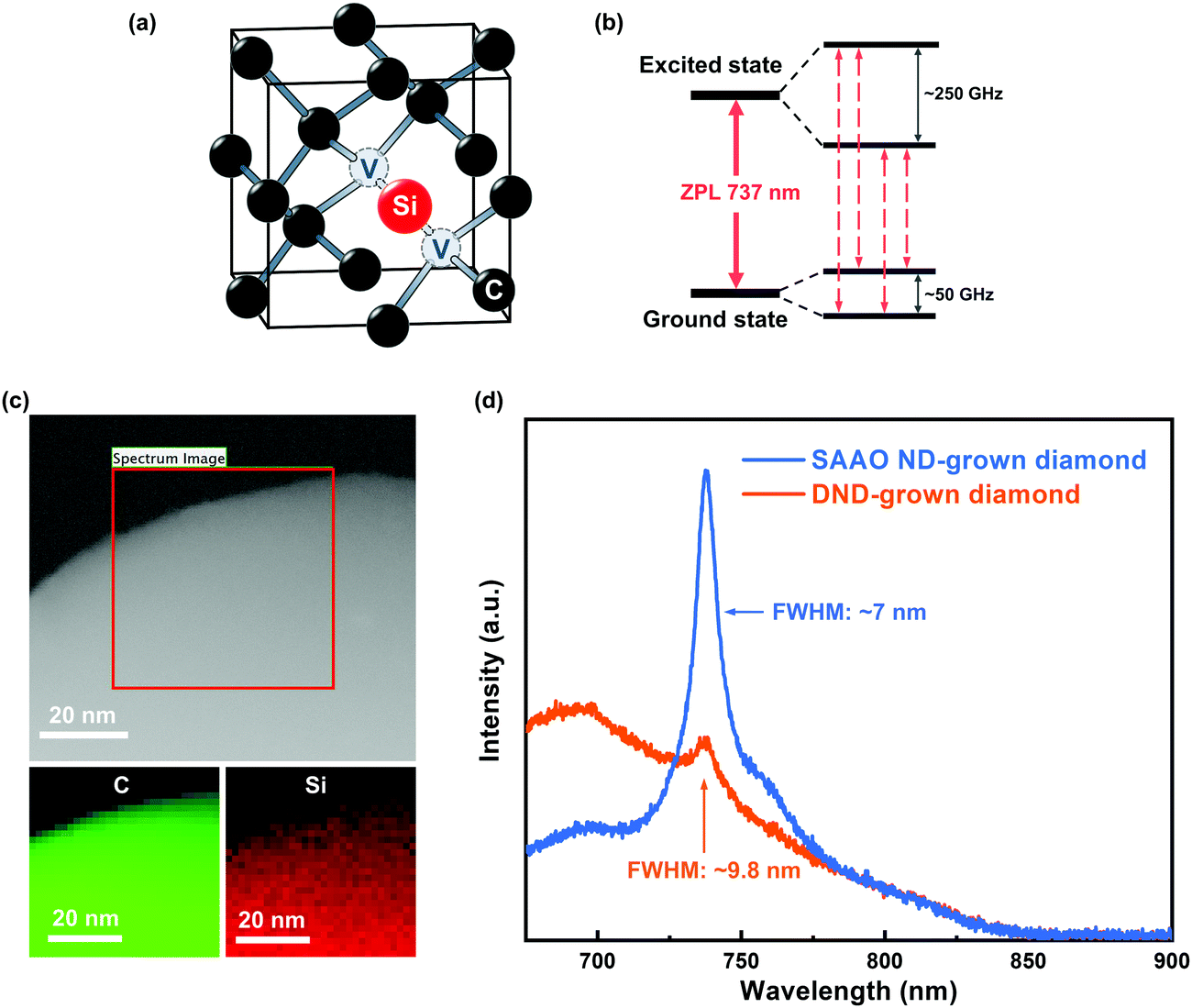 | ||
| Fig. 2 (a) Representative atomistic diagram of a SiV center with interstitial silicon (red), vacancies (gray), and carbon (black) atoms shown within a diamond unit cell. (b) The energy level scheme of the SiV center at cryogenic temperatures, showing the four optical transitions between the doublet ground and excited states. (c) STEM image and corresponding EELS elemental maps of a selected area of a SAAO ND-grown diamond microparticle. (d) The PL spectra of the DND- and SAAO ND-grown diamond microparticles containing SiV centers (532 nm as the excitation wavelength) at 25 °C. | ||
All-optical thermometry based on as-grown diamond microparticles with SiV centers
Performing high-resolution thermometry with nanoscale spatial resolution is crucial in studying multiple physiological processes in cell biology and material science.29,30 While the NV centers in diamond remain the most-studied and well adopted high-sensitive nanothermometers,31,32 most of the protocols require the involvement of microwave signals, which lead to considerable heating effects and are not suitable for a large variety of biological samples.33 Due to these measurement issues, several microwave-free all-optical temperature measurement methods based on a wide variety of diamond-based defects have been demonstrated in the last few years.34–37 As compared to other defects, SiV centers offer multiple advantages such as emission in the near-infrared (NIR) range, high Debye–Waller factor (DWF), narrow bandwidth, and high photo- and chemical stability.19,37,38 Moreover, SiV emission is linearly polarized,39 which can be used to filter out its signal from background noise, increasing the signal-to-noise ratio and contrast in fluorescence images. These factors render the SiV center a promising candidate for thermometry and bioimaging-related applications in life sciences.Recently, high sensitivity all-optical SiV based thermometry has been achieved by multiple groups.19,37,38 And the above demonstrated superior features, e.g., high crystallinity, excellent SiV property and low inhomogeneity, of the SAAO ND-grown diamond microparticles also facilitate highly sensitive, and calibration-free all-optical thermometry to be performed.
Based on previous studies,19,37 we performed SiV-based thermometry using the SAAO ND-grown diamond microparticles by measuring the ZPL position, linewidth (FWHM), and DWF, as a function of temperature (Fig. 3a–c). These parameters are extracted by performing the appropriate Lorentzian fitting to the PL spectrum19 (see Data Analysis, ESI†). Since the SiV ZPL frequency shift deviates by less than 1% from the linear approximation at room temperature,37 we performed the measurement in a small temperature range (25–35 °C). The thermal susceptibilities of the SiV ZPL position (0.0124 nm/°C) and ZPL FWHM (0.03 nm/°C) are extracted from the linear fitting of the plots in Fig. 3a and b. These values perfectly match the previously reported values measured using ultrapure bulk diamond samples,37 indicating the high crystal quality of our sample. Moreover, our measurement was performed on a large number of diamond microparticles (details can be found in the ESI†), which also suggests the low inhomogeneity among different particles.
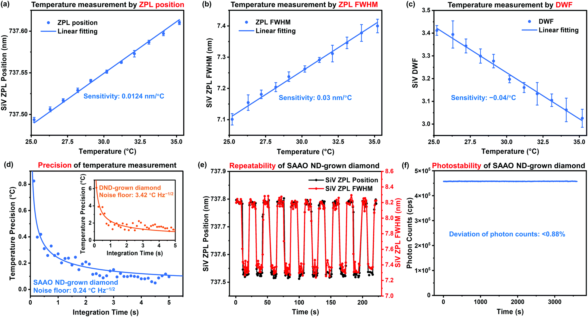 | ||
| Fig. 3 Temperature measurement using the SAAO ND-grown diamond microparticles to demonstrate ultrasensitive all-optical thermometry. A laser power of 60 mW was used, with integration time = 2.5 seconds. (a) SiV ZPL Position vs. Temperature. A sensitivity of 0.0124 nm/°C is extracted. (b) SiV ZPL FWHM vs. Temperature. A sensitivity of 0.03 nm/°C is extracted. (c) SiV DWF vs. Temperature. A sensitivity of −0.04/°C is extracted. (d) Temperature precision (σ) of the thermometer as a function of integration time (t). The solid line is a fit to the equation σ = η/(t1/2).33 The temperature uncertainty/noise floor (η) is 0.24 °C Hz−1/2 for the SAAO ND-grown diamond. The inset shows the result of the DND-grown diamond with a temperature uncertainty/noise floor (η) of 3.42 °C Hz−1/2. (e) Repeatability and long-term stability of temperature measurements. The laser power periodically shifted from 155 mW to 215 mW in a step-wise fashion, and the time trace of the fitted SiV ZPL parameters is shown. The integration time for each datapoint is 250 ms. (f) Photostability test of the SAAO ND-grown diamond. Photon counts monitored by an Andor EMCCD Camera for 1 hour, and its time trace is shown. | ||
To quantitatively evaluate the sensitivity of our thermometer, we extracted the temperature uncertainty for different integration times (t) at a fixed temperature and performed the appropriate shot-noise fitting (t−1/2), as shown in Fig. 3d. A sensitivity/noise floor (η) of 0.24 °C Hz−1/2 is extracted, comparable to the previously reported values for all-optical ND-based measurements.33 Since the measurement uncertainty follows the shot-noise limit (t−1/2),37 the sensitivity can be further improved by increasing the photon collection rates from the sample. In fact, the sensitivity can be simply enhanced by performing a multiparametric analysis, following Choi et al.'s reported novel data analysis method.19
As a comparison, we performed temperature measurements using the DND-grown diamond as well (see ESI†). The experimental conditions (laser power, integration time) were kept the same to perform a fair comparison. A significantly higher noise floor (3.42 °C Hz−1/2, shown as the inset of Fig. 3d) is observed, resulting in longer acquisition times to achieve the same temperature resolution. Moreover, higher ZPL linewidths and different thermal susceptibilities indicate inhomogenous properties among different particles, requiring separate calibration for each particle.
To further benchmark our sample and explore the scope of its applications, we measured the repeatability (Fig. 3e) and photostability (Fig. 3f) of our SAAO ND-grown diamond thermometer. To measure the temperature dynamics for our sample, we used our excitation laser as a local heat source, which offers excellent stability and efficiency. Due to the interaction between the silicon substrate and its impurities with the laser, the local temperature of the diamond is proportional to the excitation laser power applied. This allows us to use our sample as a 2-in-1 system, allowing simultaneous temperature readout and control. The excitation laser power is periodically modulated from 155 mW to 215 mW in a step-wise manner. The SiV PL spectrum is continuously measured to obtain a time trace of the fitted parameters, as shown in Fig. 3e. The ZPL position and FWHM perfectly follow the step-wise modulation of the excitation laser power, demonstrating the excellent repeatability and long-term stability of our SAAO ND-grown diamond thermometer. Furthermore, it displays excellent photostability. As shown in Fig. 3f, the photon counts are measured for 1 hour and deviate by less than 0.88% during the measurement.
Conclusion
Here, we report the fabrication of high-quality diamond microparticles on the Si substrate by CVD. Our method enables the mass production of diamond microparticles containing SiV centers with superior properties using the clean and rounded SAAO NDs as the CVD seeds. Using the fabricated high-quality sample, we have demonstrated ultrasensitive all-optical thermometry measurements with a noise floor of about 0.24 °C Hz−1/2. These findings have significant value for realizing various practical applications of high-quality diamond microparticles.Author contributions
T. T. Z., J. X. J. and Z. Q. W.: materials preparations. T. T. Z. and M. G.: materials characterizations, writing – original draft. X. Y. G. and Y. Z.: STEM and EELS measurements. Y. C. Y. and T. K. C. H.: Raman measurements. Q. W., K. H. L. and Z. Q. C.: supervision, funding acquisition, writing – review & editing.Conflicts of interest
There are no conflicts to declare.Acknowledgements
Z. Q. C. acknowledges financial support from the HKSAR Research Grants Council (RGC) Early Career Scheme (ECS, No. 27202919); HKSAR Research Grants Council (RGC) Research Matching Grant Scheme (RMGS, No. 207300313); HKSAR Innovation and Technology Fund (ITF): Platform Projects of the Innovation and Technology Support Programme (ITSP, No. ITS/293/19FP); and HKU Seed Fund for Basic Research (No. 202011159019) and Small Equipment Grant (No. 102009812). K. H. L. acknowledges financial support from the National Natural Science Foundation of China (Grant No. 62004088 and 12074170). Q. W. acknowledges financial support from the Guangdong Basic and Applied Basic Research Foundation (2019B1515120081, 2019B1515120091). Y. Z. acknowledges financial support from the Hong Kong Polytechnic University grant (No. ZVRP). The authors are grateful to Junni Zhang for her careful proofreading of this manuscript.References
- R. Schirhagl, K. Chang, M. Loretz and C. L. Degen, Annu. Rev. Phys. Chem., 2014, 65, 83–105 CrossRef CAS PubMed.
- T. Zhang, G. Pramanik, K. Zhang, M. Gulka, L. Wang, J. Jing, F. Xu, Z. Li, Q. Wei, P. Cigler and Z. Chu, ACS Sens., 2021, 6, 2077–2107 CrossRef CAS PubMed.
- M. W. Doherty, N. B. Manson, P. Delaney, F. Jelezko, J. Wrachtrup and L. C. Hollenberg, Phys. Rep., 2013, 528, 1–45 CrossRef CAS.
- T. Muller, C. Hepp, B. Pingault, E. Neu, S. Gsell, M. Schreck, H. Sternschulte, D. Steinmuller-Nethl, C. Becher and M. Atature, Nat. Commun., 2014, 5, 3328 CrossRef PubMed.
- A. M. Schrand, S. A. C. Hens and O. A. Shenderova, Crit. Rev. Solid State Mater. Sci., 2009, 34, 18–74 CrossRef CAS.
- H. Tinwala and S. Wairkar, Mater. Sci. Eng., C, 2019, 97, 913–931 CrossRef CAS PubMed.
- A. Gicquel, K. Hassouni, F. Silva and J. Achard, Curr. Appl. Phys., 2001, 1, 479–496 CrossRef.
- R. J. Nemanich, J. A. Carlisle, A. Hirata and K. Haenen, MRS Bull., 2014, 39, 490–494 CrossRef CAS.
- N. Yang, S. Yu, J. V. Macpherson, Y. Einaga, H. Zhao, G. Zhao, G. M. Swain and X. Jiang, Chem. Soc. Rev., 2019, 48, 157–204 RSC.
- J. Raymakers, K. Haenen and W. Maes, J. Mater. Chem. C, 2019, 7, 10134–10165 RSC.
- S. Handschuh-Wang, T. Wang and Y. Tang, Small, 2021, 2007529 CrossRef CAS PubMed.
- S. Stehlik, M. Varga, P. Stenclova, L. Ondic, M. Ledinsky, J. Pangrac, O. Vanek, J. Lipov, A. Kromka and B. Rezek, ACS Appl. Mater. Interfaces, 2017, 9, 38842–38853 CrossRef CAS PubMed.
- O. A. Williams, O. Douhéret, M. Daenen, K. Haenen, E. Ōsawa and M. Takahashi, Chem. Phys. Lett., 2007, 445, 255–258 CrossRef CAS.
- I. I. Vlasov, A. S. Barnard, V. G. Ralchenko, O. I. Lebedev, M. V. Kanzyuba, A. V. Saveliev, V. I. Konov and E. Goovaerts, Adv. Mater., 2009, 21, 808–812 CrossRef CAS.
- E. Neu, C. Arend, E. Gross, F. Guldner, C. Hepp, D. Steinmetz, E. Zscherpel, S. Ghodbane, H. Sternschulte, D. Steinmüller-Nethl, Y. Liang, A. Krueger and C. Becher, Appl. Phys. Lett., 2011, 98, 243107 CrossRef.
- Y. K. Tzeng, J. L. Zhang, H. Lu, H. Ishiwata, J. Dahl, R. M. Carlson, H. Yan, P. R. Schreiner, J. Vuckovic, Z. X. Shen, N. Melosh and S. Chu, Nano Lett., 2017, 17, 1489–1495 CrossRef CAS PubMed.
- K. Bray, L. Cheung, K. R. Hossain, I. Aharonovich, S. M. Valenzuela and O. Shimoni, J. Mater. Chem. B, 2018, 6, 3078–3084 RSC.
- L. J. Rogers, K. D. Jahnke, T. Teraji, L. Marseglia, C. Muller, B. Naydenov, H. Schauffert, C. Kranz, J. Isoya, L. P. McGuinness and F. Jelezko, Nat. Commun., 2014, 5, 4739 CrossRef CAS PubMed.
- S. Choi, V. N. Agafonov, V. A. Davydov and T. Plakhotnik, ACS Photonics, 2019, 6, 1387–1392 CrossRef CAS.
- K. Iakoubovskii and G. J. Adriaenssens, Diamond Relat. Mater., 2000, 9, 1349–1356 CrossRef CAS.
- E. Neu, D. Steinmetz, J. Riedrich-Möller, S. Gsell, M. Fischer, M. Schreck and C. Becher, New J. Phys., 2011, 13, 025012 CrossRef.
- S. Singh and S. A. Catledge, J. Appl. Phys., 2013, 113, 44701 CrossRef PubMed.
- T. Zhang, L. Ma, L. Wang, F. Xu, Q. Wei, W. Wang, Y. Lin and Z. Chu, ACS Appl. Nano Mater., 2021, 4, 9223–9230 CrossRef CAS.
- J. P. Goss, R. Jones, S. J. Breuer, P. R. Briddon and S. Oberg, Phys. Rev. Lett., 1996, 77, 3041–3044 CrossRef CAS PubMed.
- J. Barjon, E. Rzepka, F. Jomard, J. M. Laroche, D. Ballutaud, T. Kociniewski and J. Chevallier, Phys. Status Solidi A, 2005, 202, 2177–2181 CrossRef CAS.
- S. Malykhin, Y. Mindarava, R. Ismagilov, F. Jelezko and A. Obraztsov, Diamond Relat. Mater., 2022, 125, 109007 CrossRef CAS.
- Y. Mei, C. Chen, D. Fan, M. Jiang, X. Li and X. Hu, Nanoscale, 2019, 11, 656–662 RSC.
- B. Yang, B. Yu, H. Li, N. Huang, L. Liu and X. Jiang, Carbon, 2020, 156, 242–252 CrossRef CAS.
- M. Quintanilla and L. M. Liz-Marzán, Nano Today, 2018, 19, 126–145 CrossRef CAS.
- C. Bradac, S. F. Lim, H. C. Chang and I. Aharonovich, Adv. Opt. Mater., 2020, 2000183 CrossRef CAS.
- G. Kucsko, P. C. Maurer, N. Y. Yao, M. Kubo, H. J. Noh, P. K. Lo, H. Park and M. D. Lukin, Nature, 2013, 500, 54–58 CrossRef CAS PubMed.
- T. Plakhotnik, H. Aman and H.-C. Chang, Nanotechnology, 2015, 26, 245501 CrossRef PubMed.
- M. Fujiwara and Y. Shikano, Nanotechnology, 2021, 32, 482002 CrossRef CAS PubMed.
- T. Plakhotnik, M. W. Doherty, J. H. Cole, R. Chapman and N. B. Manson, Nano Lett., 2014, 14, 4989–4996 CrossRef CAS PubMed.
- J.-W. Fan, I. Cojocaru, J. Becker, I. V. Fedotov, M. H. A. Alkahtani, A. Alajlan, S. Blakley, M. Rezaee, A. Lyamkina, Y. N. Palyanov, Y. M. Borzdov, Y.-P. Yang, A. Zheltikov, P. Hemmer and A. V. Akimov, ACS Photonics, 2018, 5, 765–770 CrossRef CAS.
- M. Alkahtani, I. Cojocaru, X. Liu, T. Herzig, J. Meijer, J. Küpper, T. Lühmann, A. V. Akimov and P. R. Hemmer, Appl. Phys. Lett., 2018, 112, 241902 CrossRef.
- C. T. Nguyen, R. E. Evans, A. Sipahigil, M. K. Bhaskar, D. D. Sukachev, V. N. Agafonov, V. A. Davydov, L. F. Kulikova, F. Jelezko and M. D. Lukin, Appl. Phys. Lett., 2018, 112, 203102 CrossRef.
- W. Liu, M. N. A. Alam, Y. Liu, V. N. Agafonov, H. Qi, K. Koynov, V. A. Davydov, R. Uzbekov, U. Kaiser, T. Lasser, F. Jelezko, A. Ermakova and T. Weil, Nano Lett., 2022, 22, 2881–2888 CrossRef CAS PubMed.
- Y. Liu, G. Chen, Y. Rong, L. P. McGuinness, F. Jelezko, S. Tamura, T. Tanii, T. Teraji, S. Onoda, T. Ohshima, J. Isoya, T. Shinada, E. Wu and H. Zeng, Sci. Rep., 2015, 5, 12244 CrossRef PubMed.
Footnotes |
| † Electronic supplementary information (ESI) available. See DOI: https://doi.org/10.1039/d2tc01090a |
| ‡ These authors contributed equally to this work. |
| This journal is © The Royal Society of Chemistry 2022 |