
 Open Access Article
 This Open Access Article is licensed under a
 Creative Commons Attribution 3.0 Unported Licence
Enhancing hole carrier injection via low electrochemical doping on circularly polarized polymer light-emitting diodes†‡
Hao
Yan
 a,
Jessica
Wade
a,
Li
Wan
b,
Sooncheol
Kwon
*c,
Matthew J.
Fuchter
*de,
Alasdair J.
Campbell§
a and
Ji-Seon
Kim
*a
a,
Jessica
Wade
a,
Li
Wan
b,
Sooncheol
Kwon
*c,
Matthew J.
Fuchter
*de,
Alasdair J.
Campbell§
a and
Ji-Seon
Kim
*a
aDepartment of Physics and Centre for Processable Electronics, Imperial College London, London, SW7 2AZ, UK. E-mail: ji-seon.kim@imperial.ac.uk
bDepartment of Physics Chemistry and Biology (IFM), Linköping University, Linköping 581 83, Sweden
cDepartment of Energy and Materials Engineering, Dongguk University-Seoul, Seoul, 04620, Republic of Korea. E-mail: kwansc12@dongguk.edu
dDepartment of Chemistry and Molecular Sciences Research Hub, Imperial College London, White City Campus, 80 Wood Lane, London, W12 OBZ, UK. E-mail: m.fuchter@imperial.ac.uk
eCentre for Processable Electronics, Imperial College London, London, SW7 2AZ, UK
First published on 1st June 2022
Abstract
Circularly polarized electroluminescence (CP-EL) from a blend system of chiral small-molecule additives and device optimised achiral π-conjugated polymers (π-CPs) is of great interest for next-generation display technologies. However, CP polymer light-emitting diodes can suffer from unbalanced charge transport and unfavorable energetics between chiral additives and achiral polymers, which can limit the efficiency of charge injection and device performance. Herein, we demonstrate the use of a small amount of chemcially modified electrochemical doping agent (EDA, 1.5 wt%) to control such limitations. The EDA with a long cationic alkyl chain enables strong hydrophobicity and stable electrochemical doping of achiral π-CP F8BT in F8BT:aza[6]H blends, which allows for better charge injection and balance. This leads to improved device performance while maintaining highly dissymmetric electroluminescence (gEL ∼ 0.50@580 nm) and an inverted dissymmetry factor (gEL = −0.65@525 nm). These findings indicate that EDAs may provide a simple approach to improve the performance of CP optoelectronic devices.
Introduction
Ionic liquids consisting of two ions of opposite charges have been demonstrated as additives that improve the optoelectronic performance of various devices, including solar cells,1,2 polymer light-emitting diodes (PLEDs)3,4 and organic gas sensors.5,6 Only small quantities of ionic liquids are required to enhance the device performance while maintaining the original film morphology. For example, Snaith and coworkers recently reported a highly efficient planar perovskite solar cell with markedly improved long-term stability and power conversion efficiency after the incorporation of only 0.3 mol% 1-butyl-3-methylimidazolium tetrafluoroborate ([BMIM]+[BF4]−) ionic liquid in the perovskite active layer.1We have demonstrated that the incorporation of a chemically modified ionic liquid (0.5 wt%), 1-dodecly-3-imidazolium hexafluoro-phosphate ([C1C12IM]+[PF6]−), into the active layer of PLEDs can improve device performance.3 The long alkyl chain of the cations in [C1C12IM]+[PF6]− was shown to have a strong interaction with the light-emitting polymer (here, poly(9,9-dioctylfluorene-alt-benzothiadiazole), F8BT), which resulted in a reduction in the current turn-on voltage (VJ) and luminous turn-on voltage (VL) values (from 20 V to 12 V, 1200 nm-thick F8BT) and extension of the device lifetime (by 37%) due to efficient charge injection and balance.3,7 Employing in situ electric field-dependent Raman spectroscopy we revealed that the improved device performance is due to the strong electrochemical interaction between F8BT and [C1C12IM]+[PF6]− (hereafter referred to as the electrochemical doping agent, EDA).8 To further explore the potential of this approach, we questioned whether the addition of an EDA may benefit more advanced optoelectronic devices with complex blend systems, such as the achiral polymer – chiral additives used in circularly polarized PLEDs (CP-PLEDs).9
The direct CP electroluminescence (CP-EL) emission from CP-PLEDs has been proposed to be a simple, cost-effective way to improve the performance of state-of-the-art display technologies and has attracted interest for use in 3D displays, spintronics and optical data storage.9–12 In such devices, the extent to which the emitted light is CP is defined by the dissymmetry factor, g, defined as g = 2 (IL − IR)/(IL + IR), where IL and IR are the intensities of left-handed and right-handed CP light, respectively.10,13 Fuchter, Campbell and coworkers have demonstrated that annealed thin films of blends consisting of a conventional (achiral) electroluminescent polymer and a chiral small molecule additive, 1-aza[6]helicene (hereafter, aza[6]H), can exhibit a considerable chiroptical response due to the induction of a chiral phase within the polymer.9,14–18 One of the challenges in developing high-performance CP-PLEDs is to identify chiral small molecule additives that (i) have appropriate energy levels to facilitate efficient charge injection and transport and (ii) induce the chiral phase.
The first F8BT:aza[6]H CP-PLEDs (gEL ∼ 0.2) exhibited a higher VL of 6.2 V at 1 cd m−2 and a lower luminous efficiency (K < 2 cd A−1) than neat F8BT PLEDs (VL ∼ 5 V, K ∼ 4 cd A−1).7 In these early devices, the origins of high turn-on voltages and poor efficiencies might be associated with hole injection problems and a shifted electron–hole recombination zone (closer to the anode).10–12 After carefully optimizing the solution concentration and active layer thickness, the performance of F8BT:aza[6]H devices has improved considerably (gEL ∼ 1.0, K ∼ 4 cd A−1, VL ∼ 5.2 V).14,19 The use of an inverted device architecture and sublimable charge transport layers has since been shown to enhance performance even further (K ∼ 16.4 cd A−1, VL ∼ 2.3 V).15,20 Despite these advances, the performance of achiral polymer – chiral additive blend systems can still be inferior to their neat achiral polymer counterparts. Highly dissymmetric CP emission has also been observed in PLEDs where the active layers comprise of related materials, such as (i) conjugated polymers with chiral side chains or (ii) achiral polymer – chiral additive blends with liquid crystal alignment layers.21,22 Such devices still exhibit high VL (>10 V) and poor luminance, with |gEL| that is sensitive to the position of the recombination zone.9,16–18,21,22
Considering the benefits of the EDA in non-CP PLEDs, we questioned whether a combination of three components (i.e., an achiral polymer, a chiral small-molecule additive and the EDA) may present an alternate approach to improve the performance of CP-PLEDs. The key challenge is to maximize the ternary synergetic effect for improved device efficiencies while maintaining the chiral polymer phase that gives rise to high |gEL|. Herein, we demonstrate that the EDA (1.5 wt%), F8BT and aza[6]H (10 wt%) can form a homogeneous ternary blend system that enables CP-PLEDs to exhibit efficient charge carrier injection and balance whilst maintaining a high |gEL|. Through the use of advanced spectroscopic probes (in situ Raman spectroscopy and Ambient Photoemission Spectroscopy, APS), we attribute this improved performance to electrochemical doping of F8BT by the EDAs. We show that EDAs can improve device performance, even in a ternary blend system, and demonstrate them as a simple approach to improve the performance of CP optoelectronic devices.
Results and discussion
Optical characterizations of materials and device architecture
The chemical structures of F8BT, right-handed [P] aza[6]H and EDA are shown in Fig. 1(a). A conventional device architecture was used (ITO/PEDOT:PSS/TFB/F8BT or F8BT:aza[6]H/Ca/Al, where ITO is indium tin oxide, PEDOT:PSS is poly(3,4-ethylenedioxythiophene)polystyrene sulfonate, and TFB is poly[(9,9-dioctylfluorenyl-2,7-diyl)-co-(4,4′-(N-(4-sec-butylphenyl) diphenylamine))]) (Fig. 1(b)).3,9 For all devices the active layer thickness (t) was 190 nm. In the case of annealed (140 °C, 10 min) neat F8BT and F8BT:EDA(1.5 wt%) blend films, there is negligible circular dichroism (CD) close to the F8BT absorption band (see ESI,‡ Fig. S1). The same is not true for the F8BT:aza[6]H or F8BT:aza[6]H:EDA blends. Interestingly, the introduction of 1.5 wt% EDA does not appear to diminish the chiroptical response (Fig. 1(c) and (d)). In fact, the photoluminescence (PL) of F8BT:aza[6]H:EDA had a slightly higher degree of dissymmetry than that of F8BT:aza[6]H (gPL = 0.08 vs. 0.05) (see detail information in the ESI,‡ Fig. S2). These results indicated that EDA mixes well with F8BT:aza[6]H and does not interfere with the formation of the chiral phase.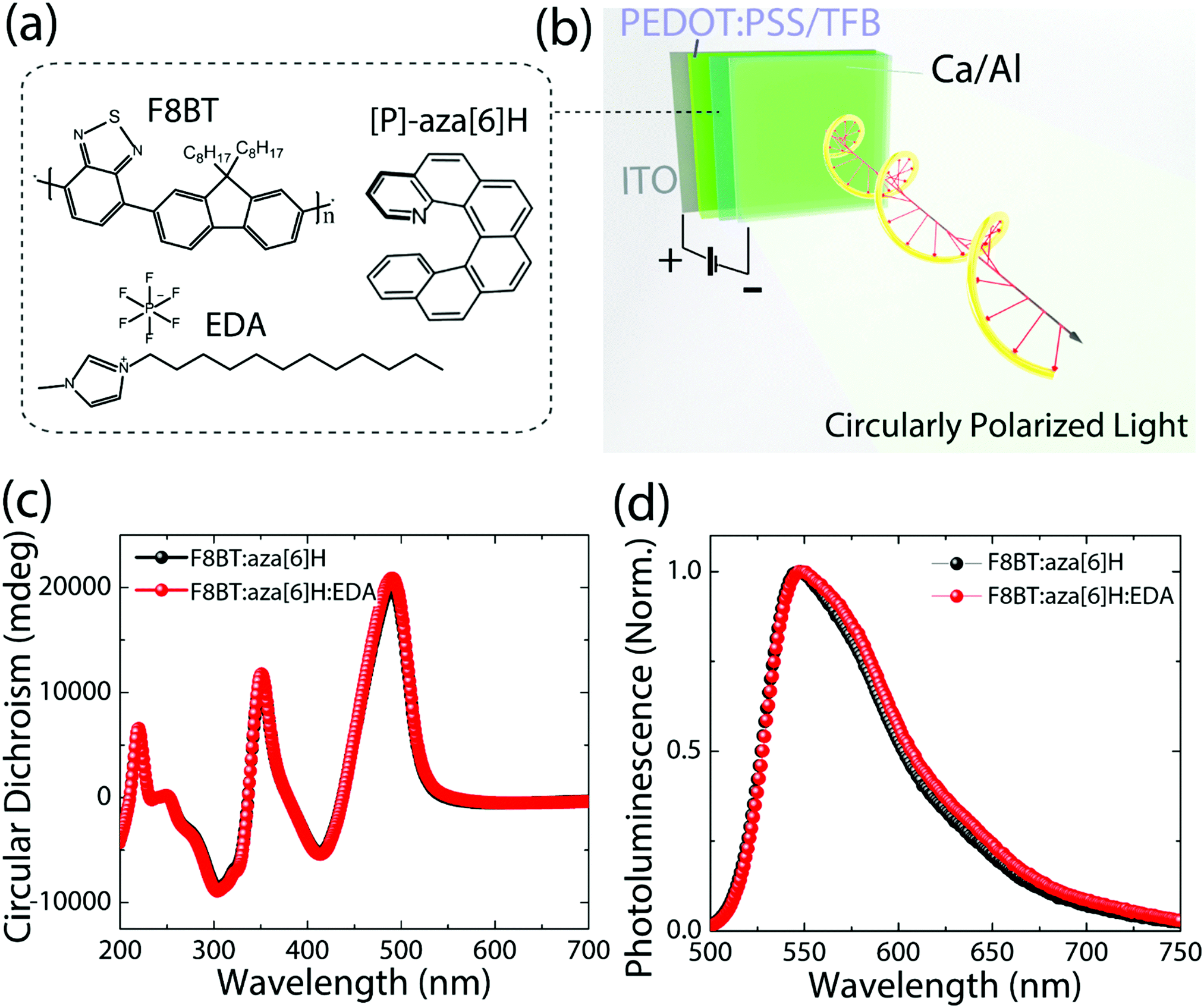 | ||
| Fig. 1 (a) and (b) Chemical structures of F8BT, EDA and [P]-aza[6]H in the conventional PLED device architecture of ITO/PEDOT:PSS/TFB/EML/Ca/Al. (c) and (d) CD spectra and normalized photoluminescence spectra of annealed F8BT:aza[6]H and F8BT:aza[6]H:EDA thin films. | ||
To study the energy levels of each component in the ternary blend system, we performed APS.23–26 The highest occupied molecular orbital (HOMO) levels of neat F8BT, F8BT:aza[6]H, F8BT:aza[6]H:EDA and neat aza[6]H films (all annealed, t = 190 nm on top of an Au substrate) were extracted by the extrapolation of the photoemission signals (Fig. 2). The HOMO levels of neat F8BT, F8BT:aza[6]H and F8BT:aza[6]H:EDA were determined to be ∼5.71 eV. The same HOMO levels measured for the neat and blend samples indicated that the energetics of the blend films were not disturbed by the aza[6]H nor EDA.15 The HOMO level of neat aza[6]H is measured to be ∼5.9 eV using an extrapolation of the photoemission signals in the linear regime, as used in other organic molecules. Interestingly, it is often observed that below the HOMO threshold, there is an additional area (shaded area down to ∼5.7 eV for aza[6]H) in which measurable photoemission signals still exist. These signals indicate energetic disorder of aza[6]H small molecules in a neat thin film, possibly originated from different orientations of aza[6]H molecules in the thin film leading to energetic inhomogeneity. Such orientation dependent HOMO energy levels are also observed in other small molecules such as a-6T (see ESI,‡ Fig. S3).26
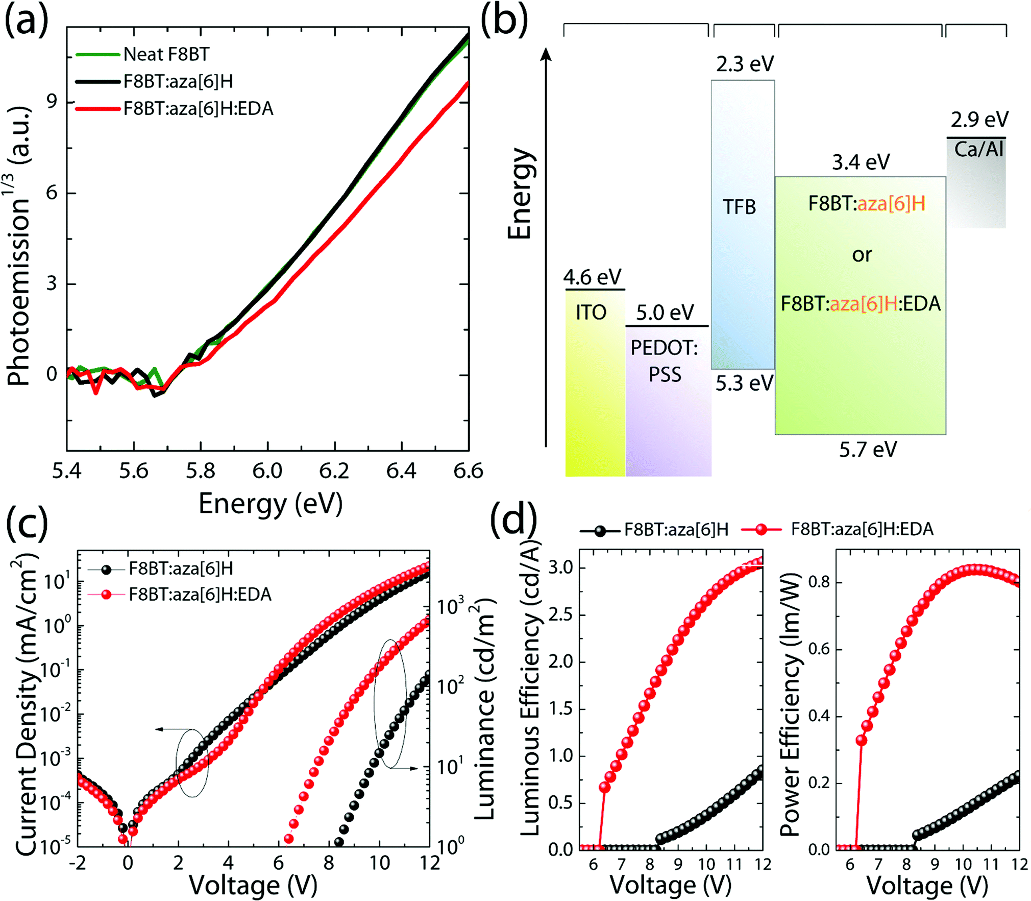 | ||
| Fig. 2 (a) APS spectra of the neat F8BT, F8BT:aza[6]H and F8BT:aza[6]H:EDA. (b) Energy diagram of each layer in the F8BT:aza[6]H or F8BT:aza[6]H:EDA CP-PLED architecture. (c) Comparison of the current density–voltage–luminance (J–V–L) characteristics of the F8BT:aza[6]H and F8BT:aza[6]H:EDA CP-PLEDs. (d) Comparison of the luminance efficiency and power efficiency. | ||
To compare the performances of F8BT, F8BT:aza[6]H and F8BT:aza[6]H:EDA PLEDs, current density–voltage–luminance (J–V–L) characteristics were measured (Fig. 2(c)). Compared with the neat F8BT devices, the current density and luminance of F8BT:aza[6]H PLEDs are reduced by more than one order of magnitude (from 102 mA cm−2 to 16 mA cm−2, and from 3723 cd m−2 to 141 cd m−2 at 12 V) with increased VL from 4.9 V to 8.3 V (see the details in ESI,‡ Table S1 and Fig. S4), which reduces the luminous and power efficiencies from 3.8 cd A−1 to 0.8 cd A−1 and from 1.4 lm W−1 to 0.2 lm W−1, respectively. Interestingly, such reduced device performance in F8BT:aza[6]H blends was partly recovered in F8BT:aza[6]H:EDA ternary blends. With the addition of 1.5 wt% EDA, the VL of F8BT:aza[6]H:EDA was reduced from 8.3 V to 6.3 V with improved efficiencies from 0.8 cd A−1 to 3.1 cd A−1 and from 0.2 lm W−1 to 0.9 lm W−1. At the same current density (70 mA cm−2), the luminance of F8BT:aza[6]H:EDA PLEDs increased from 1018 cd m−2 to 2115 cd m−2, which is comparable to that of the neat F8BT PLEDs (2549 cd m−2) (see ESI,‡ Fig. S4c). This indicates that residual charge carriers exist in F8BT:aza[6]H without contributing to useful radiative recombination. The addition of the EDA facilitates more efficient charge carrer recombination. Notably, F8BT:aza[6]H:EDA PLEDs exhibited clear and sharp current turn-on at 3.5 V, which indicates efficient hole injection (discussed more below), thereby reducing VL (Fig. 2(c) and (d)). To establish whether the improvement in device performance due to the EDA held across all F8BT polymer molecular weights (i.e., not specific to the low molecular weight F8BT discussed above), the same device characterization was performed with F8BT with a higher molecular weight (MW = 21 K) (see ESI,‡ Fig. S5), and the same improvement in charge injection, luminous and power efficiencies was observed.
Impact of the EDA on the CP emission of F8BT:aza[6]H PLEDs
Maintaining strongly dissymmetric emission (high gEL) is essential to demonstrate that EDAs can be added to improve the performance of CP optoelectronic devices. As seen in Fig. 3, the F8BT:aza[6]H and F8BT:aza[6]H:EDA PLEDs both achieve gEL = 0.50@580 nm, compared with negiligible gEL of the neat F8BT PLED (see ESI,‡ Fig. S6).3,27 Owing to formation of a chiral phase in F8BT after blending with aza[6]H, the EL lineshape of F8BT:aza[6]H is different to that of the neat F8BT, and there is a considerable increase in the intensity of left-handed CP-EL (IL).14,22 For the F8BT:aza[6]H:EDA blend, there is a slight broadening in the left-handed emission and a dramatic change in the relative intensity of the emission peaks (525 nm and 580 nm) for right-handed EL. These differences lead to an inverted dissymmetry factor (gEL = −0.65@525 nm). To understand this additional peak at 525 nm for F8BT:aza[6]H:EDA, the thickness-dependent EL spectra for neat F8BT are shown in the ESI,‡ Fig S8. The thick (t = 110 nm) neat F8BT PLED show strong microcavity effects with a main emission peak at 580 nm and a shoulder at 525 nm. Upon doping 1.5 wt% EDA, the EL lineshape changes significantly, due to either strong enhanced emission at 525 nm or quenched emission at 580 nm (ESI,‡ Fig S8b). These can be attributed to the shifted recombination zone that arises due to the EDA, which results in enhanced charge injection and balance and a weak microcavity effect. This result might indicate a preferred interaction of EDA molecules with neat, achiral F8BT instead of F8BT in the chiral phase, which enhances charge injection and maintains strong gEL, thereby changing the EL shape (see ESI,‡ Fig. S7) and inverting the handedness of CP light.14,27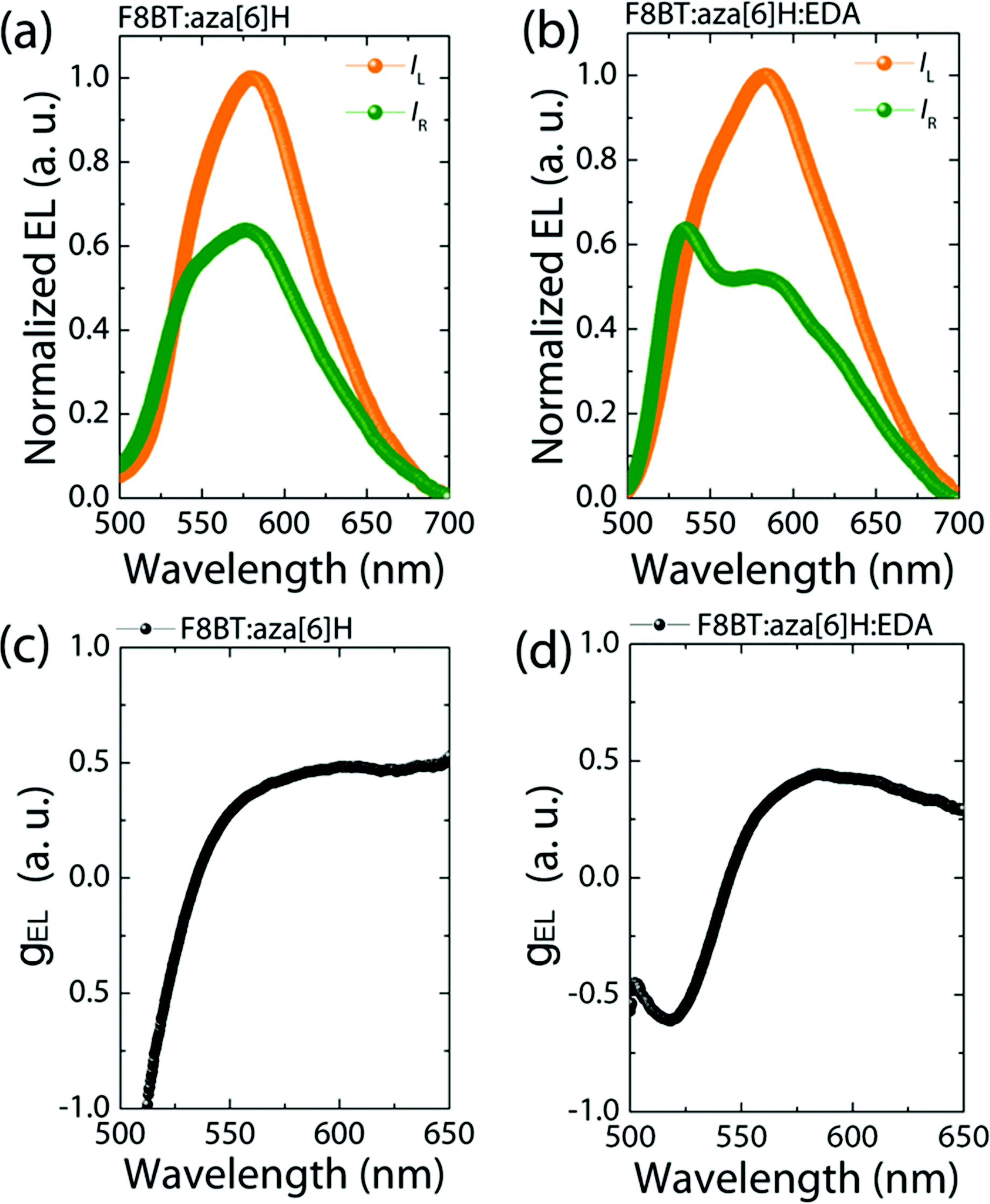 | ||
| Fig. 3 Measured CP-EL spectra (a), (b) and corresponding calculated gEL values (c) (d) of F8BT:aza[6]H and F8BT:aza[6]H:EDA CP-PLEDs. | ||
To investigate the effects of energetic disorder in blends and the EDA electrochemical doping on charge injection, hole-only devices ITO/PEDOT:PSS/TFB/active layer/MoO3/Au were fabricated (detailed information provided in the Experimental section).28–30 The combination of efficient hole injection from the ITO/PEDOT:PSS/TFB interface and effective electron blocking at the MoO3/Au interface resulted in the F8BT:aza[6]H:EDA devices exhibiting a sharper turn-on at 3 V and a 3-order-of-magnitude higher current density at 10 V than the F8BT:aza[6]H device (Fig. 4(a)). In particular, the current turn-on voltage of hole-only device was in exact coincidence with that of F8BT:aza[6]H:EDA CP-PLEDs (Vturn-on ∼ 3.5 V) in Fig. 2(d). These features described above supports the idea that the EDA induces strong electrochemical doping of F8BT, even in a ternary blend system, which leads to a significant increase in hole current and improved charge balance.31
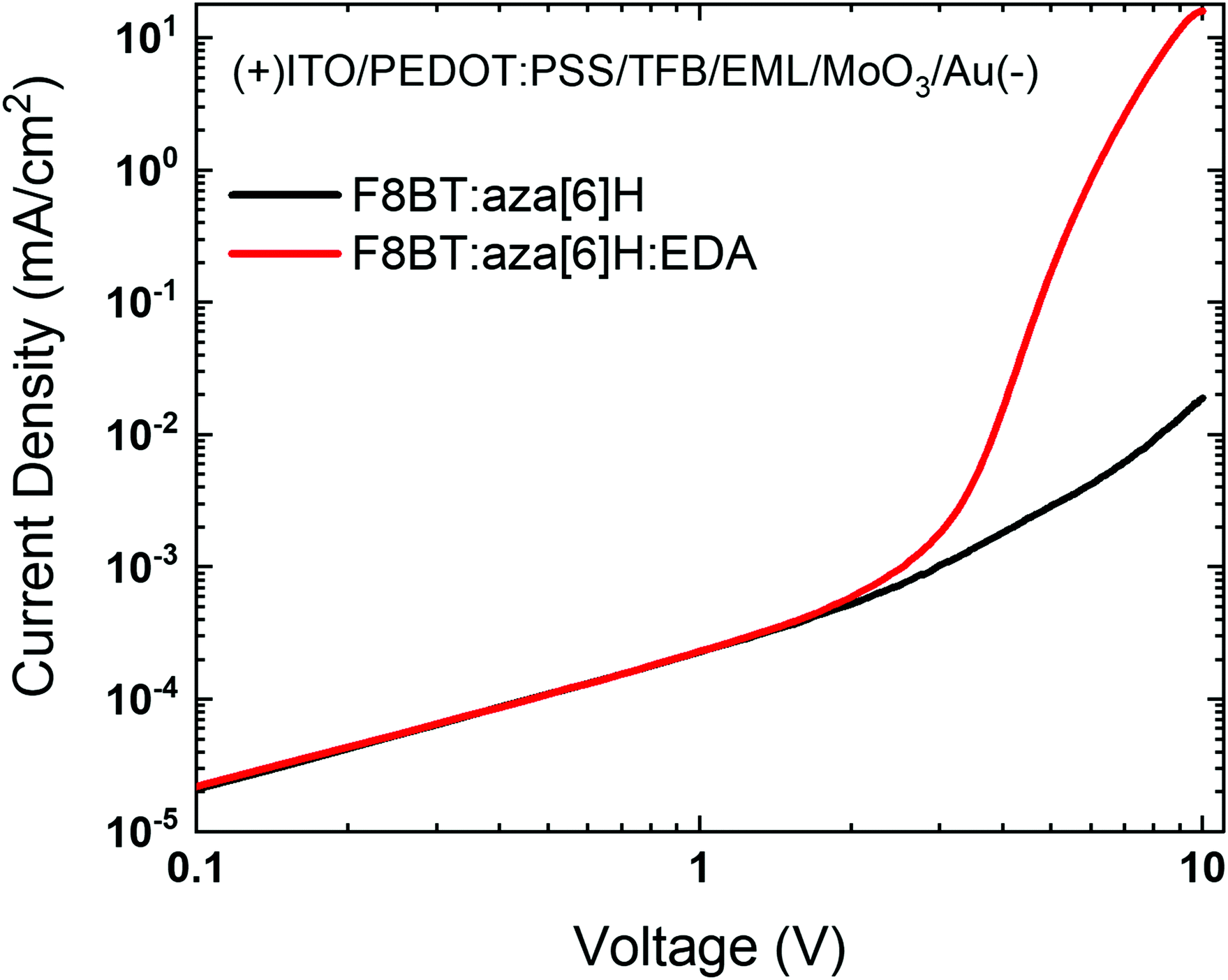 | ||
| Fig. 4 (a) J–V characteristics of the F8BT:aza[6]H and F8BT:aza[6]H:EDA hole-only devices (ITO/PEDOT:PSS/TFB/EML/MoO3/Au). | ||
Proposed mechanism for improved device efficiency via electrochemical doping in ternary electroactive blends
We have previously suggested aza[6]H acts as a hole trap as it aggregates close to the hole injection interface.15,32,33 To further study whether the spatial distribution of aza[6]H throughout the active layer may influence charge carrier injection, we turned to surface-enhanced Raman spectroscopy (SERS).15,32,33 The localized electric field generated by surface plasmons on the gold substrate can result in the selective enhancement of the Raman modes of the molecules accumulated at that interface. Whilst the Raman spectra are dominated by Raman modes associated with the F8BT (e.g. 1341, 1545 and 1608 cm−1), a vibrational signature of aza[6]H occurs at 1360 cm−1.14 Owing to the localized electric field generated by surface plasmons on gold substrates, the relative intensity of the aza[6]H peak intensity (1360 cm−1) is enhanced strongly in F8BT:aza[6]H Au films (I1360/I1341 increases from 1.1 to 1.9) compared to those deposited on a quartz substrate. The increase in I1360/I1341 is maintained upon annealing. This indicates that aza[6]H is mainly accumulated at the gold/F8BT interface for both pristine and annealed films (ESI,‡ Fig. S9). As the shallow tail states and HOMO of the aza[6]H are close to the HOMO of F8BT (see ESI,‡ Fig. S3), holes injected from the PEDOT:PSS/TFB anode become trapped in this aza[6]H layer, thereby limiting direct hole injection to the F8BT during device operation.34To further probe the mechanisms that underpin the improved charge injection and balance, we performed electric field dependent Raman spectroscopy. Here, we monitored the intermolecular interactions and/or electronic coupling in PLEDs under applied bias (0 V to 10 V). Fig. 5(a) and 5(b) shows the Raman spectra of the main backbone ring stretching modes of F8BT (1545 cm−1 and 1608 cm−1 for BT and F8 units, respectively) in F8BT:aza[6]H and F8BT:aza[6]H:EDA PLEDs.3,35,36 For F8BT:aza[6]H PLED, the Raman spectrum does not show any significant changes when the applied voltage was increased from 0 to 10 V. In contrast, the overall intensity of the main F8BT peaks of F8BT:aza[6]H:EDA PLEDs decrease gradually as a function of applied bias. As the applied voltage increases from 0 to 10 V, the intensities of the 1545 cm−1 and 1608 cm−1 peaks decrease by ∼5% and ∼10%, respectively (Fig. 5(b)). Such a reduction in F8BT peak intensity is an important signature of the formation of hole polarons in F8BT.3,5,6 Note the larger quenching of the F8 ring mode, which indicates that during F8BT:aza[6]H:EDA device operation, the electrochemical doping process occurs between the F8 unit and EDA, generating more hole polarons in F8 units.3,5 There is no further quenching of the 1608 cm−1 peak at high voltages (9 V and 10 V).
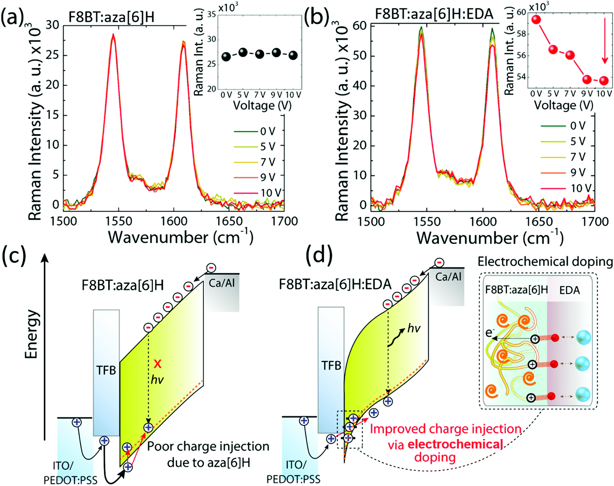 | ||
| Fig. 5 (a) and (b) In situ electric-field-dependent Raman spectra of the F8BT:aza[6]H and F8BT:aza[6]H:EDA devices, respectively. The inset figures indicate the changes in the selective Raman peaks at 1608 cm−1 under an electric field ranging from 0 V to 10 V. (c) and (d) The proposed mechanism of poor charge injection in F8BT:aza[6]H and improved charge injection and charge balance in an EDA-doped device via the electrochemical doping by EDA molecules (inset), respectively. | ||
Based on the results above, owing to the similar HOMO level of aza[6]H to the F8BT, the holes injected from the PEDOT:PSS/TFB anode can be trapped by the aza[6]H in F8BT:aza[6]H PLEDs, which limits direct charge injection to the emissive F8BT and reduces radiative recombination (Fig. 5(c)). However, when an EDA is introduced, a strong electrochemical interaction with F8BT increases charge injection and charge balance, without sacrificing important CP-EL, and thereby considerably improving device performance (Fig. 5(d)).
Conclusions
In conclusion, we have demonstrated a simple and efficient approach for producing single-layer, solution-processed CP-PLEDs based on a ternary synergetic system comprising an achiral conjugated polymer, chiral small molecules and electrochemical dopants. We found that the EDA with strong hydrophobicity and ionic properties can enable the stable and molecular-level electrochemical doping of F8BT even in F8BT:aza[6]H blends, which improves charge injection, reduces VL and ultimately improves device efficiencies without compromising CP-EL emission. The results demonstrate EDAs as a simple but effective way to improve the charge injection and transport properties of many other organic devices such as organic solar cells, transistors and sensors.5,6,37,38Experimental
Materials
F8BT was synthesized by Cambridge Display Technology, Inc., UK and used as received. The average molecular weight of F8BT was 9 kg mol−1. Aza[6]H was prepared as previously reported.9 The EDA, [C1C12IM]+[PF6]− was synthesized through a conventional method described elsewhere.3,6Solution preparation
F8BT, aza[6]H and the EDA were directly dissolved in toluene. All solutions were stirred for 10 h in the dark under ambient conditions.UV-vis absorption, photoluminescence spectroscopy and thin-film characterization
Quartz substrates were cleaned using acetone and isopropyl alcohol via sequential sonication for 5 min. F8BT:aza[6]H or F8BT:aza[6]H:EDA layers were spin-coated on quartz substrates using the same solutions and were annealed at 140 °C/10 min for both thin films and PLEDs. UV-vis absorption was measured using a Shimadzu UV-2550 UV-visible spectrophotometer. Photoluminescence spectra (PL) were recorded in a reflection geometry using a Jobin Yvon Horiba Fluoromax-3 spectrofluorometer (excitation wavelength: 420 nm).Device fabrication and characterization for PLED applications
ITO-patterned glass substrates (size: 12 mm × 8 mm) were cleaned in an ultrasonic bath using acetone, isopropyl alcohol and detergent (15 min), followed by washing in DI water two times and baking at 115 °C (10 min). After a 3 min UV-ozone treatment, a 40 nm-thick PEDOT:PSS layer was spin-coated onto the ITO substrate, which was then heated at 145 °C (15 min). Then, a 15 nm-thick hole-transporting and electron-blocking TFB interlayer was spin-coated on top of the PEDOT:PSS layer, and the assembly was baked under nitrogen at 180 °C (1 h). Subsequently, an emissive layer of F8BT:aza[6]H or F8BT:aza[6]H:EDA was spin-coated from a toluene solution and annealed at 140 °C (10 min). Finally, calcium (25 nm) and aluminum (100 nm) cathodes were deposited via thermal evaporation under vacuum conditions (1 × 10⁻⁷ Torr). For SCLC measurements, F8BT:aza[6]H or F8BT:aza[6]H:EDA in a 40 mg ml−1 solution was used to obtain 190 nm-thick layers. The thicknesses of the MoO3 and Au layers deposited by evaporation were 10 nm and 100 nm, respectively.For the CP-PLED device measurements, the J–V–L characteristics and efficiencies were measured using a Keithley 2400 source meter and a Minolta LS100 spot luminance meter under dark conditions. EL spectra were recorded using an Ocean Optics universal serial bus 2000 (USB 2000) charge-coupled device (CCD) spectrometer equipped with a fiber light collection bundle. All PLED measurements were carried out within a nitrogen-filled test chamber.
APS and SPV measurements
A Kelvin Probe technology APS-04 instrument was used to evaluate the energetics of neat F8BT, F8BT:aza[6]H and F8BT:aza[6]H:EDA thin films. For APS measurements, the gold substrate-based sample was illuminated with UV light from a monochromatic deuterium lamp source (4–7 eV). Test samples were ∼190 nm-thick organic thin films spin-coated on SiO2/Au substrates. The metal Au substrate ensured proper grounding of the organic thin films so that correct values of the tip-sample potential difference could be obtained.In situ electric-field-dependent Raman spectroscopy measurements
In situ Raman spectra of the PLED samples were collected using a specially designed chamber equipped with a probe station and a Renishaw inVia Raman microscope (50X objective lens). Measurements were performed with a 633 nm excitation laser source operated at 0.5 mW using an acquisition time of 2 seconds and an applied external voltage from 0 V to 10 V. A defocused laser beam with a diameter of 8 μm and flowing N2 gas were used to avoid photodegradation of the samples.Conflicts of interest
A. Campbell and M. Fuchter are inventors on a patent concerning chiral blend materials (WO2014016611).Acknowledgements
We acknowledge the UK Engineering and Physical Sciences Research Council (EPSRC), Plastic Electronics Doctoral Training Centre (EP/G037515/1) and Cambridge Display Technology Ltd. for supplying the TFB and F8BT polymers. MJF acknowledges the EPSRC for an Established Career Fellowship (EP/R00188X/1). In addition, we gratefully acknowledge support from the Global Research Laboratory Program of the National Research Foundation (NRF) funded by the Ministry of Science, ICT & Future Planning (NRF-2017K1A1A2013153) and the Young Researchers Program of the NRF funded by the Ministry of Science, ICT & Future Planning (NRF-2021R1A2C4001904).References
- S. Bai, P. Da, C. Li, Z. Wang, Z. Yuan, F. Fu, M. Kawecki, X. Liu, N. Sakai, J. T. Wang, S. Huettner, S. Buecheler, M. Fahlman, F. Gao and H. J. Snaith, Nature, 2019, 571, 245–250 CrossRef CAS PubMed.
- C. Li, X. Liu, D. Tu, Q. Yang, X. Chen, C. Li and X. Guo, Chem. Commun., 2019, 55, 2956–2959 RSC.
- H. Yan, S. Limbu, X. Wang, J. Nightingale, I. Hamilton, J. Wade, S. Kwon, K. Lee and J. S. Kim, Adv. Funct. Mater., 2019, 29, 1904092 CrossRef.
- S. Sato, S. Ohisa, Y. Hayashi, R. Sato, D. Yokoyama, T. Kato, M. Suzuki, T. Chiba, Y. J. Pu and J. Kido, Adv. Mater., 2018, 30, 1705915 CrossRef PubMed.
- K. Stewart, S. Limbu, J. Nightingale, K. Pagano, B. Park, S. Hong, K. Lee, S. Kwon and J.-S. Kim, J. Mater. Chem. C, 2020, 8, 15268–15276 RSC.
- S. Kwon, Y. Pak, B. Kim, B. Park, J. Kim, G. Kim, Y. R. Jo, S. Limbu, K. Stewart, H. Kim, B. J. Kim, S. Y. Jang, H. Kang, J. W. Min, J. S. Kim, G. Y. Jung and K. Lee, J. Mater. Chem. A, 2020, 8, 16884–16891 RSC.
- C. Hoven, R. Yang, A. Garcia, A. J. Heeger, T. Q. Nguyen and G. C. Bazan, J. Am. Chem. Soc., 2007, 129, 10976–10977 CrossRef CAS PubMed.
- S. Wood, J. R. Hollis and J. S. Kim, J. Phys. D: Appl. Phys., 2017, 50, 073001 CrossRef.
- Y. Yang, R. C. da Costa, D. M. Smilgies, A. J. Campbell and M. J. Fuchter, Adv. Mater., 2013, 25, 2624–2628 CrossRef CAS PubMed.
- J. M. Han, S. Guo, H. Lu, S. J. Liu, Q. Zhao and W. Huang, Adv. Opt. Mater., 2018, 6, 1800538 CrossRef.
- M. Li, S. H. Li, D. Zhang, M. Cai, L. Duan, M. K. Fung and C. F. Chen, Angew. Chem., Int. Ed., 2018, 57, 2889–2893 CrossRef CAS PubMed.
- F. Y. Song, Z. Xu, Q. S. Zhang, Z. Zhao, H. K. Zhang, W. J. Zhao, Z. J. Qiu, C. X. Qi, H. Zhang, H. H. Y. Sung, I. D. Williams, J. W. Y. Lam, Z. J. Zhao, A. J. Qin, D. G. Ma and B. Z. Tang, Adv. Funct. Mater., 2018, 28, 1800051 CrossRef.
- D. W. Zhang, M. Li and C. F. Chen, Chem. Soc. Rev., 2020, 49, 1331–1343 RSC.
- L. Wan, J. Wade, F. Salerno, O. Arteaga, B. Laidlaw, X. Wang, T. Penfold, M. J. Fuchter and A. J. Campbell, ACS Nano, 2019, 13, 8099–8105 CrossRef CAS PubMed.
- L. Wan, J. Wade, X. Shi, S. Xu, M. J. Fuchter and A. J. Campbell, ACS Appl. Mater. Interfaces, 2020, 12, 39471–39478 CrossRef CAS PubMed.
- J. Wade, J. N. Hilfiker, J. R. Brandt, L. Liiro-Peluso, L. Wan, X. Shi, F. Salerno, S. T. J. Ryan, S. Schoche, O. Arteaga, T. Javorfi, G. Siligardi, C. Wang, D. B. Amabilino, P. H. Beton, A. J. Campbell and M. J. Fuchter, Nat. Commun., 2020, 11, 6137 CrossRef CAS PubMed.
- L. Wan, J. Wade, X. Wang, A. J. Campbell and M. J. Fuchter, J. Mater. Chem. C, 2022, 10, 5168–5172 RSC.
- L. Wan, X. Shi, J. Wade, A. J. Campbell and M. J. Fuchter, Adv. Opt. Mater., 2021, 9, 2100066 CrossRef CAS.
- D. Kabra, L. P. Lu, M. H. Song, H. J. Snaith and R. H. Friend, Adv. Mater., 2010, 22, 3194–3198 CrossRef CAS PubMed.
- B. R. Lee, E. D. Jung, J. S. Park, Y. S. Nam, S. H. Min, B. S. Kim, K. M. Lee, J. R. Jeong, R. H. Friend, J. S. Kim, S. O. Kim and M. H. Song, Nat. Commun., 2014, 5, 4840 CrossRef CAS PubMed.
- D. Di Nuzzo, C. Kulkarni, B. Zhao, E. Smolinsky, F. Tassinari, S. C. J. Meskers, R. Naaman, E. W. Meijer and R. H. Friend, ACS Nano, 2017, 11, 12713–12722 CrossRef CAS PubMed.
- D. M. Lee, J. W. Song, Y. J. Lee, C. J. Yu and J. H. Kim, Adv. Mater., 2017, 29, 1700907 CrossRef PubMed.
- M. Daboczi, I. Hamilton, S. Xu, J. Luke, S. Limbu, J. Lee, M. A. McLachlan, K. Lee, J. R. Durrant, I. D. Baikie and J. S. Kim, ACS Appl. Mater. Interfaces, 2019, 11, 46808–46817 CrossRef CAS PubMed.
- M. Daboczi, J. Kim, J. Lee, H. Kang, I. Hamilton, C. T. Lin, S. D. Dimitrov, M. A. McLachlan, K. Lee, J. R. Durrant and J. S. Kim, Adv. Funct. Mater., 2020, 30, 2001482 CrossRef CAS.
- J. Y. Wu, J. Lee, Y. C. Chin, H. F. Yao, H. Cha, J. Luke, J. H. Hou, J. S. Kim and J. R. Durrant, Energy Environ. Sci., 2020, 13, 2422–2430 RSC.
- Y. Dong, V. C. Nikolis, F. Talnack, Y. C. Chin, J. Benduhn, G. Londi, J. Kublitski, X. Zheng, S. C. B. Mannsfeld, D. Spoltore, L. Muccioli, J. Li, X. Blase, D. Beljonne, J. S. Kim, A. A. Bakulin, G. D'Avino, J. R. Durrant and K. Vandewal, Nat. Commun., 2020, 11, 4617 CrossRef PubMed.
- M. Suh, J. Bailey, S. W. Kim, K. Kim, D. J. Yun, Y. Jung, I. Hamilton, N. Chander, X. Wang, D. D. Bradley, D. Y. Jeon and J. S. Kim, ACS Appl. Mater. Interfaces, 2015, 7, 26566–26571 CrossRef CAS PubMed.
- Y. A. Zhang and P. W. M. Blom, Appl. Phys. Lett., 2011, 98, 143504 CrossRef.
- A. J. Campbell, D. D. C. Bradley and D. G. Lidzey, J. Appl. Phys., 1997, 82, 6326–6342 CrossRef CAS.
- X. Shi, V. Nádaždy, A. Perevedentsev, J. M. Frost, X. Wang, E. von Hauff, R. C. I. MacKenzie and J. Nelson, Phys. Rev. X, 2019, 9, 021038 CAS.
- N. B. Kotadiya, H. Lu, A. Mondal, Y. Ie, D. Andrienko, P. W. M. Blom and G. A. H. Wetzelaer, Nat. Mater., 2018, 17, 329–334 CrossRef CAS PubMed.
- J. Razzell-Hollis, Q. Thiburce, W. C. Tsoi and J. S. Kim, ACS Appl. Mater. Interfaces, 2016, 8, 31469–31481 CrossRef CAS PubMed.
- S. D. Chao-Yu Li, J. Yi, C. Wang, P. M. Radjenovic, Z.-Q. Tian and J.-F. Li, Sci. Adv., 2020, 6, eaba6012 CrossRef PubMed.
- Q. Niu, R. Rohloff, G. A. H. Wetzelaer, P. W. M. Blom and N. I. Craciun, Nat. Mater., 2018, 17, 557–562 CrossRef CAS PubMed.
- C. L. Donley, J. Zaumseil, J. W. Andreasen, M. M. Nielsen, H. Sirringhaus, R. H. Friend and J. S. Kim, J. Am. Chem. Soc., 2005, 127, 12890–12899 CrossRef CAS PubMed.
- H. Yan, T. W. Tseng, S. Omagari, I. Hamilton, T. Nakamura, M. Vacha and J. S. Kim, J. Chem. Phys., 2022, 156, 074704 CrossRef CAS PubMed.
- J. Li, C. Hou, C. Huang, S. Xu, X. Peng, Q. Qi, W. Y. Lai and W. Huang, Research, 2020, 2020, 3839160 CAS.
- J. Li, X. Peng, C. Huang, Q. Qi, W.-Y. Lai and W. Huang, Polym. Chem., 2018, 9, 5278–5285 RSC.
Footnotes |
| † Dedication: to the memory of Professor Alasdair James Campbell. |
| ‡ Electronic supplementary information (ESI) available. See DOI: https://doi.org/10.1039/d2tc01010k |
| § Deceased. |
| This journal is © The Royal Society of Chemistry 2022 |