
Light-emitting Ti2N (MXene) quantum dots: synthesis, characterization and theoretical calculations†
Anir S.
Sharbirin
 a,
Shrawan
Roy
a,
Trang Thu
Tran
a,
Sophia
Akhtar
a,
Jaspal
Singh
a,
Dinh Loc
Duong
*ab and
Jeongyong
Kim
*a
a,
Shrawan
Roy
a,
Trang Thu
Tran
a,
Sophia
Akhtar
a,
Jaspal
Singh
a,
Dinh Loc
Duong
*ab and
Jeongyong
Kim
*a
aDepartment of Energy Science, Sungkyunkwan University, Suwon 16419, Korea. E-mail: j.kim@skku.edu
bCenter for Integrated Nanostructure Physics (CINAP), Institute for Basic Science (IBS), Suwon 16419, Republic of Korea. E-mail: ddloc@skku.edu
First published on 30th March 2022
Abstract
MXene-based quantum dots (MQDs), which are obtained by fragmenting MXenes into a nanometer scale, can display photoluminescence (PL), suggesting light-emitting applications for bandgap-less MXenes. However, despite the diverse possible formations of MXene components, only carbide MXene-based MQDs have been reported to emit light. In this study, we synthesized water-soluble MQDs with an average diameter of 3.14 nm using the titanium nitride (Ti2N) MXene. Ti2N MQDs exhibited efficient PL, with a maximum quantum yield of 7.5%, upon light absorption over the deep UV wavelength range of 400–230 nm. The density functional theory calculations and PL excitation measurements identified a bandgap of 3.8 eV and the existence of an unfulfilled band (E1) between the occupied low-energy (E0) and unoccupied high-energy (E2) bands, which induces strong absorption in deep UV energy originating from the E0–E2 transition. Light-emitting nitride MQDs expand and facilitate the UV optoelectronic applications of MQDs.
1. Introduction
Two-dimensional (2D) MXenes (general formula: Mn+1XnTx, where M is an early transition metal, X is either C, N, or C and N, and Tx is the notation of the surface-terminating functional groups, such as O, OH, F, and H)1–6 have the properties of high conductivity, flexibility, and non-toxicity.1,7–10 MXenes are obtained by chemically etching out A-elements from MAX phases and there are approximately 150 different types of MAX phases currently available.11 Thus, MXenes with various combinations of constituting elements have been studied for energy storage devices, sensors, electromagnetic interference, solar cells, catalysis, transparent conductors, and photothermal and plasmonic applications.1,2,6–8,12–16 However, MXenes are generally absent in the bandgap and only theoretical calculations predict a very small bandgap (<0.1 V),1 limiting their use in optoelectronic applications.In 2017, Xue et al. obtained the Ti3C2 MXene via a hydrothermal process. The resulting Ti3C2 MXene was several nanometers in size and displayed efficient photoluminescence (PL), which originated from the quantum confinement effect.13 These MXene-based quantum dots (MQDs)13,17–23 have been extensively studied for applications in light-emitting diodes (LEDs), catalysis, biosensors, photothermal therapy, energy storage, and bioimaging.13,17–32 While mostly carbide group MQDs have been studied so far,13,17,25,33–35 nitride or carbonitride MXenes have higher expected electronic conductivity and better stability in solution than carbide MXenes3,5 and are thus promising precursors of MQDs. Recently, Shao et al. synthesized MQDs based on the Ti2N MXene and demonstrated their biodegradability and biocompatibility; however, their light-emitting properties were not discussed.23
In this study, we report the synthesis of light-emitting Ti2N MQDs, which displayed a strong PL upon deep UV absorption down to a wavelength of 230 nm. Light emission was confirmed from both the aqueous solution and film dispersion. The PL excitation (PLE) measurements and density functional theory (DFT) calculations revealed the origins of efficient light emission and absorption in deep UV energy. Our results substantially expand the application of MQDs in UV optoelectronic devices.
2. Experimental
Materials
Ti2AlN MAX phase powder (200-mesh) and Ti2AlC MAX phase powder (200-mesh) were purchased from Shanghai Xinglu Chemical Technology Co. Ltd, Shanghai, China. Hydrochloric acid (HCl) and potassium fluoride (KF) were purchased from Merck Korea, Seoul, Republic of Korea. All other chemicals were of analytical grade and directly used as is.Sample preparation
The Ti2N MXene was prepared by etching the Al layer of the Ti2AlN MAX phase using a mixture of HCl and KF powder.5,23 Specifically, 6 M HCl (100 mL) was added to KF powder (6 g) and continuously stirred until the solution was well mixed. The solution (20 mL) was added to the Ti2AlN MAX phase powder and left at room temperature for 3 h to selectively etch the Al layer. Afterward, the solution was heated at 40 °C with bath sonication (1 h) to promote intercalation, which aided the exfoliation process. The obtained suspension of Ti2N MXene was washed multiple times using deionized water and centrifuged (12![[thin space (1/6-em)]](https://www.rsc.org/images/entities/char_2009.gif) 000 rpm) for 20 min to remove the soluble fluorides. Fluoride removal was performed until the pH was close to 6 to obtain the Ti2N MXene powder. Ti2N MQDs were synthesized from Ti2N MXene powder based on a previous procedure for synthesizing carbide MQDs by adjusting chemical concentrations.13 Specifically, the Ti2N MXene powder (1.1 g) was dispersed in deionized water (10 mL) and added to a 50 mL Teflon-lined stainless-steel autoclave. Ammonium hydroxide (NH4OH) was added slowly until the solution reached a pH of 10. Then, the autoclave was kept in a vacuum oven at 100 °C for 6 h. The resulting mixture was centrifuged at 10000 rpm for 20 min and the supernatant of Ti2N MQDs was collected. Ti2C MQDs were prepared using the same procedure as that used for synthesizing Ti2N MQDs. Ti2C MXene precursor was obtained from the Ti2AlC MAX phase with 10% HF as the etchant.
000 rpm) for 20 min to remove the soluble fluorides. Fluoride removal was performed until the pH was close to 6 to obtain the Ti2N MXene powder. Ti2N MQDs were synthesized from Ti2N MXene powder based on a previous procedure for synthesizing carbide MQDs by adjusting chemical concentrations.13 Specifically, the Ti2N MXene powder (1.1 g) was dispersed in deionized water (10 mL) and added to a 50 mL Teflon-lined stainless-steel autoclave. Ammonium hydroxide (NH4OH) was added slowly until the solution reached a pH of 10. Then, the autoclave was kept in a vacuum oven at 100 °C for 6 h. The resulting mixture was centrifuged at 10000 rpm for 20 min and the supernatant of Ti2N MQDs was collected. Ti2C MQDs were prepared using the same procedure as that used for synthesizing Ti2N MQDs. Ti2C MXene precursor was obtained from the Ti2AlC MAX phase with 10% HF as the etchant.
Structural characterization
The structural characterization of powder X-ray diffraction (XRD) was performed using an X-ray diffractometer (D2 Phaser, Bruker). The images of the exfoliated layers of Ti2N and Ti2N MXene were obtained using scanning electron microscopy (SEM) (JSM-7600F, JEOL) and the etching of Al was confirmed using energy-dispersive X-ray spectroscopy (EDS) (X-Max, Oxford Instrument). The morphologies of the Ti2N MQDs were further analyzed using high-resolution transmission electron microscopy (HRTEM) (JEM-3010, JEOL) and atomic force microscopy (AFM) (XE-120, Park Systems).Optical characterization
The vibration modes and crystal structures of the Ti2N MXene-based samples were determined using a Raman confocal microscope (alpha300 SR, WITec GmbH). The UV-Vis absorption and PL spectra of the Ti2N MQD solutions were analyzed using an absorption spectrometer (Optizen, K Lab) and a fluorescence spectrophotometer (Cary Eclipse, Agilent), respectively. A thin film of Ti2N MQDs was prepared by drop-casting on top of a quartz substrate, and the confocal PL was measured using a lab-made laser confocal microscope combined with a spectrometer. The laser light was focused using an objective lens (100×, 0.95 NA), and the scattered light was collected using the same objective lens and then guided to a 50 cm long monochromator equipped with a cooled charge-coupled device (CCD) (PIXIS 400, Princeton Instruments). A diode laser with an excitation wavelength of 405 nm was employed for confocal PL measurements. For quantum yield (QY) measurements, a commercial QY spectrometer (Quantaurus-QY, Hamamatsu Photonics) and a lab-made QY measurement system, which consisted of an integrating sphere (819C-SL-3.3, Newport) combined with a spectrometer equipped with a CCD (PIXIS 400, Princeton Instruments), were used and Rhodamine 6G (R6G) was used as the reference.36 Epifluorescence images were captured using an electron-multiplying CCD (EMCCD) camera (Photon MAX 512, Princeton Instruments) cooled to −70 °C. A mercury halide lamp was used as the light source and a 430 nm dichroic mirror was used to send the light into the sample through the objective lens. The light was then collected into the objective lens and a 450 nm long-pass filter was used to separate the emission from the light source.3. Results and discussion
Synthesis and structural analysis of the Ti2N MXene
The synthesis of light-emitting Ti2N MQDs is schematically presented in Fig. 1A (details are provided in the Methods section). The Ti2N MXene was obtained by chemically etching the Al layer of the Ti2AlN MAX phase, followed by a hydrothermal method, to produce the light-emitting Ti2N MQDs. The XRD results for the Ti2N MXene and Ti2AlN are presented in Fig. 1B. First, we note that most of the characteristic XRD peaks of Ti2AlN MAX phases, such as the (106), (110), and (0010) peaks, disappeared in the Ti2N XRD spectrum. Furthermore, Ti2N displayed the broadening of the (002) peak (denoted as (002*) here) and the emergence of a new (002) peak at 9.52°, which indicates that the Al layer was mostly removed from the Ti2AlN MAX phase, expanding the distance between the Ti2N layers. The small upshift of the (103) peak is also attributed to the expansion of the Ti2N layers along the (002) plane.37 A broad peak at around 30° is the reflection from the (004) plane, the presence of which is consistent with previous XRD results of the Ti2N MXene.5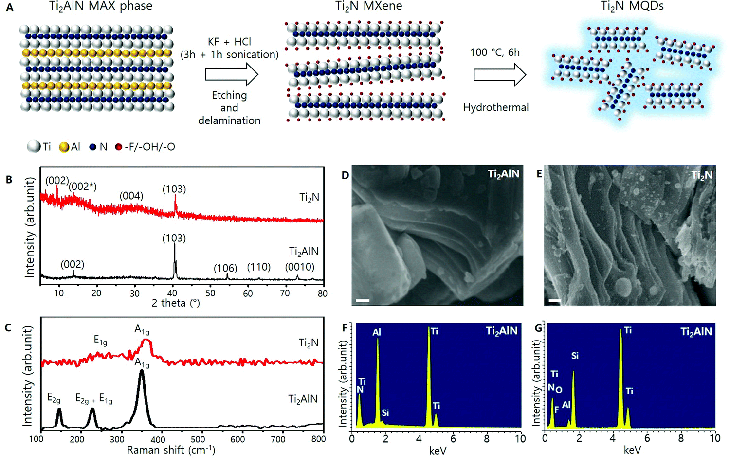 | ||
| Fig. 1 (A) Schematic of the synthesis of Ti2N MXene-based quantum dots (MQDs). (B) XRD spectra of the Ti2AlN MAX phase and Ti2N MXene. (C) Raman spectra of Ti2AlN and Ti2N. (D) SEM image of Ti2AlN (scale bar = 100 nm). (E). SEM image of Ti2N (scale bar = 100 nm). (F) EDS spectrum of the Ti2AlN MAX phase. G. EDS spectrum of the Ti2N MXene. | ||
Fig. 1C illustrates the Raman spectra of Ti2AlN and the Ti2N MXene. The Raman spectrum of the Ti2AlN samples (black curve) exhibited three Raman modes at 146, 224.4, 228.4, and 349.9 cm−1, which were identified as E2g, E2g + E1g, and A1g modes, respectively.5 The Raman spectrum of the Ti2N MXene sample (red curve) showed peaks at 250.4 and 359.7 cm−1 which can be assigned to E1g and A1g modes, originating from in-plane and out-of-plane vibrations, respectively, concerning the Ti atomic planes. The absence of the E2g mode at 146 cm−1 (generated from Ti–Al bonding) ensured the removal of Al from Ti2AlN during chemical etching. Thus, the Raman studies confirmed the successful etching of Al atoms from Ti2AlN and the formation of the Ti2N MXene.
The surface morphologies of Ti2AlN and Ti2N were analyzed by SEM and are presented in Fig. 1D and 1E, which show the compact morphology of Ti2AlN and the delamination of the crystals by the etching process in the Ti2N MXene, respectively. With the etched Al atoms, the layers between the MXene were readily intercalated. During the sonication process, the intercalation of water and K+ rigorously helped to exfoliate the MXene layers and avoid restacking during etching.5,23 To determine the variations in the atomic percentages between the Ti2AlN and Ti2N MXene, EDS measurements were performed, and the results are shown in Fig. 1F and G, respectively. The relative intensity of the Al peak at 1.5 keV was significantly reduced for Ti2N compared to Ti2AlN. The EDS spectrum of the Ti2N MXene also exhibited minor signals for O and F due to the terminating groups, –OH, −F or both, that may have emerged during exfoliation, which also indicates the successful exfoliation of Ti2AlN and formation of the Ti2N MXene.5,23
Transmission electron microscopy (TEM) images of the Ti2N MQDs are shown in Fig. 2A, where the average diameter was estimated to be 3.14 nm (Fig. 2C), substantially smaller than that (∼5 nm) of previously reported Ti2N MQDs.23 The standard deviation was only 0.2 nm, showing good uniformity of diameter. We also fabricated Ti2C MQDs via the same hydrothermal route as that used for Ti2N MQD synthesis and the obtained MQDs were relatively small with a lateral size of 2.75 nm and a narrower lattice spacing of 0.16 nm, as shown in Fig. S1 (ESI†). The observed diameter and lattice spacing were consistent with those of previous carbide MQDs.13,17,38 The MQDs were easily dispersed on a glass substrate, which also showed an average height of ∼3.5 nm in the AFM image (Fig. 2D), consistent with the estimation of the MQD diameter by TEM.
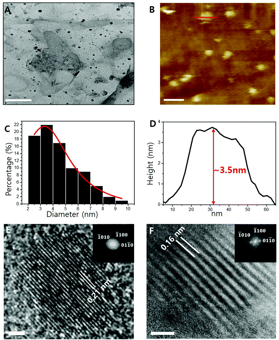 | ||
| Fig. 2 (A) TEM image of Ti2N MQDs (scale bar = 100 nm). (B) AFM image of Ti2N MQDs (scale bar = 50 nm). (C) Size distribution histogram of Ti2N MQDs obtained from the TEM image. The solid line is the Gaussian fit of the distribution (A). (D) Cross-sectional height profile of Ti2N MQDs (along the red line shown in the AFM image [B]). (E). HR-TEM image of Ti2N MQDs (scale bar = 1 nm). (F) HR-TEM image of the Ti2N MXene (scale bar = 5 nm). Insets of (E) and (F) are the corresponding FFT patterns of the HR-TEM images. | ||
HRTEM revealed the crystal structure of the as-prepared Ti2N MQDs, exhibiting lattice fringes with an inner-plane spacing of 0.21 nm (Fig. 2E), corresponding to the (01![[1 with combining macron]](https://www.rsc.org/images/entities/char_0031_0304.gif) 0) facet of the MXene. This value was slightly larger than 0.16 nm for the same inner-plane spacing of Ti2N MXene (Fig. 2F), which could be due to the effect of the intracrystalline pressure induced by the surface oxide layers of each MQD repelling each other.37,39 The repelling-induced equivalent negative pressure40 expands the lattice spacing with the decreasing size of the MQDs. This effect is more prevalent in which the lattice spacing is expanded because of the relatively higher surface-to-volume ratio of the Ti2N MQDs.37,39,40 The fast Fourier transform (FFT) pattern of MQDs (inset of Fig. 2E) shows that the Ti2N MQDs retain the hexagonal structure of the pristine Ti2N MXene. The Ti2N MQDs maintained the (010), (100), and (010) facets of the Ti2N MXene, confirming that Ti2N MQDs mostly preserve the crystal structure of the precursor Ti2N MXene. The low reaction temperature and surface-terminated -NH groups from the NH4OH solution help to maintain the crystal structure of the pristine MXene, preventing the formation of TiO2 or TiO2 quantum dots.13 The absence of C atoms in the chemical formula of the Ti2N MXene, which was further confirmed by the EDS results, ruled out the formation of light-emitting carbon dots which may occur during the synthesis of carbide-group MQDs.
0) facet of the MXene. This value was slightly larger than 0.16 nm for the same inner-plane spacing of Ti2N MXene (Fig. 2F), which could be due to the effect of the intracrystalline pressure induced by the surface oxide layers of each MQD repelling each other.37,39 The repelling-induced equivalent negative pressure40 expands the lattice spacing with the decreasing size of the MQDs. This effect is more prevalent in which the lattice spacing is expanded because of the relatively higher surface-to-volume ratio of the Ti2N MQDs.37,39,40 The fast Fourier transform (FFT) pattern of MQDs (inset of Fig. 2E) shows that the Ti2N MQDs retain the hexagonal structure of the pristine Ti2N MXene. The Ti2N MQDs maintained the (010), (100), and (010) facets of the Ti2N MXene, confirming that Ti2N MQDs mostly preserve the crystal structure of the precursor Ti2N MXene. The low reaction temperature and surface-terminated -NH groups from the NH4OH solution help to maintain the crystal structure of the pristine MXene, preventing the formation of TiO2 or TiO2 quantum dots.13 The absence of C atoms in the chemical formula of the Ti2N MXene, which was further confirmed by the EDS results, ruled out the formation of light-emitting carbon dots which may occur during the synthesis of carbide-group MQDs.
Optical properties and characterization of Ti2N MQDs
Solubility in water is an important property, especially for biomedical applications.13,17,18,22,27,29,34 The synthesized Ti2N MQDs were all well dispersed in water. Fig. S2 (ESI†) shows the blue emission from Ti2N MQDs dispersed in water upon illumination with an UV (250 nm) LED. Fig. 3A shows the PL spectra of the Ti2N MQDs with varying excitation energies. Our Ti2N MQDs displayed PL emission at an excitation wavelength of less than 280 nm. To our knowledge, this is the first demonstration of PL emission from MQDs with an excitation wavelength of less than 280 nm. A large energy difference between the excitation and emission in the range of 0.5–2 eV was previously observed for MQDs13,17,22,25,27,28,30,35 and other 2D material-derived QDs41,42 which have been attributed to surface state-aided exciton recombination. The PL emission peak was observed at approximately 3.0 eV with an excitation wavelength between 230 and 270 nm and then gradually red-shifted with increasing excitation wavelength, similar to previously developed carbide MQDs.13,17,25,35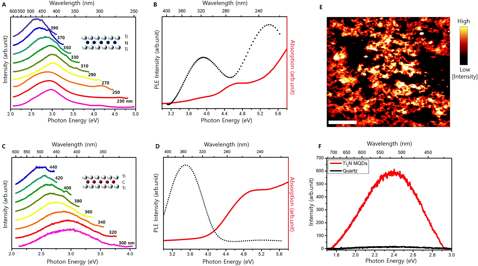 | ||
| Fig. 3 (A) PL spectra of Ti2N MQDs with varying excitation wavelengths from 230 nm to 390 nm. (B) UV-Vis absorption and PLE spectra of Ti2N MQDs. (C) PL spectra of Ti2C MQDs with varying excitation wavelengths from 260 nm to 440 nm. (D) UV-Vis absorption and PLE spectra of Ti2C MQDs. (E) Epifluorescence image of Ti2N MQDs (scale bar = 20 μm). (F) The corresponding PL spectrum of thin film Ti2N MQDs under 405 nm laser excitation. | ||
Absorption and PLE spectroscopy were performed on the Ti2N MQDs and the results are shown in Fig. 3B (black curve). Two peaks at 3.9 and 5.4 eV were observed, which is consistent with the observation of two absorption edges of the absorption spectrum (red curve). The efficient absorption of UV light below 280 nm and the consequent PL emission have not been previously observed in MQDs. A previously developed carbide MQD, Ti3C2 MQDs, displayed a PL emission peak at 3.0 eV, with a PLE peaking at 3.9 eV.13 V2C and Nb2C MQDs displayed PL-emission peaks at 2.8 and 2.4 eV, respectively.34,35 We prepared MQDs using the Ti2C MXene as the main precursor and Fig. 3C shows a series of normalized PL spectra of the Ti2C MQDs obtained with laser excitation of varying wavelengths (300–440 nm). We observed a similar gradual redshift of the PL peak with increasing excitation wavelength. The highest PL emission was obtained with a laser excitation of 350 nm, where only one peak of PLE of Ti2C MQDs was observed at 3.5 eV (Fig. 3D), which is consistent with previous Ti2C MQDs.38 Below 300 nm, PL was too weak to be detected consistently, with only one absorption edge at approximately 4.0 eV, in contrast to the presence of two absorption edges and two PLE peaks of the Ti2N MQDs. Our results indicate that Ti2N MQDs are more efficient in deep UV absorption and the consequent light emission than carbide MQDs, which suggests the advantage of Ti2N MQDs for UV applications compared to carbide MQDs.
The QY of Ti2N MQDs was estimated using the comparative method and the highest QY was estimated to be 7.5% with 320 nm (∼3.9 eV) excitation, where the peak was observed in the PLE (details of QY estimation and the plot of QY vs. excitation energy are given in Fig. S4, ESI†). The QY of our Ti2N MQDs was observed to be stable for ten days in aqueous solution under ambient conditions (Fig. S5, ESI†). We dispersed the Ti2N MQDs on a quartz substrate and observed a clear PL upon 430 nm excitation, as shown in the epifluorescence image of dispersed MQDs (Fig. 3E). The confocal scanning PL of solid dispersed Ti2N MQDs excited with a 405 nm wavelength laser was performed, and the PL intensity map is shown in Fig. S3 (ESI†).
Fig. 3F shows a PL peak at 2.4 eV, with slightly less energy than the PL peak at 2.6 eV obtained from the solution-dispersed Ti2N MQDs at 400 nm excitation. This discrepancy in the PL peak position is attributed to the variation of the dielectric environment, where the PL peak energy tends to decrease in the solid form compared to the polar solvent.43,44 To the best of our knowledge, this is the first report of PL emission and the spectra of solid dispersed MQDs. Our developed Ti2N MQDs can be excited and emitted in the form of a thin film with a wide range of excitation wavelengths. Our Ti2N MQDs demonstrated high tolerance in pH variation and the PL and QY were virtually constant for the pH range of 2–12 (Fig. S6, ESI†). On contrary, the PL intensity of Ti2N MQDs was drastically quenched when solutions of Co2+ or Mn2+ ions were added (Fig. S7, ESI†), exhibiting an outstanding capability to detect environmentally harmful heavy metal ions.
Origins of the light absorption and emission of Ti2N MQDs
DFT calculations of the density of states (DOS) of a Ti2NO2 MQD were performed as shown in Fig. 4A. The surface of the Ti2N MXene or MQD requires functionalization by O2, -OH, or -F to be stabilized in structure.1,5,17 In our case of MQDs in water environment, O2 is the most likely functional group of Ti2N MQDs. We also conducted the calculation of band structure without O2 functionalization and found that Ti–O bonding has a critical effect on the band structure of Ti2NO2 MQDs (Fig. S9, ESI†). DOS calculations of Ti2NO2 identified three energy bands of the valence band, conduction band, and higher-energy conduction band which are denoted as E0, E1, and E2, respectively. Normally, absorption occurs between E0 (N (2p) and O (2p)) and E1 (Ti (3d)) or E0 and E2 (Ti (3d)) but PL is observed only by the transition between E1 and E0.41,45–48 We also observed a single peak PL around 3.0 eV and two absorption edges at 3.8 and 5.4 eV, which is consistent with the DFT calculation results discussed above. Furthermore, the values of E1–E0 (3.8 eV) and E2–E0 (5.3 eV) given by the calculated DOS are in good agreement with the observed PLE peaks. The almost constant PL peak position above 3.9 eV excitation observed in the excitation wavelength-dependent PL measurement in Fig. 3C is the result of the absorption from E0 to E2 and the consequent electron relaxation, followed by exciton recombination at the conduction band edge. We observed a similar gradual redshift (blueshift) of the PL peak with increasing excitation wavelength (energy) due to the involvement of DOS at higher energy states within the conduction band (E1).17,28–30 Additionally, we calculated the band structure of the Ti2NO2 MQDs that were 3.0 nm in diameter (Fig. S8, ESI†), which showed a similar result, including the bandgap energy. This implies that varying the size of the MQDs is not an efficient way to tune the bandgap of the Ti2N MQDs.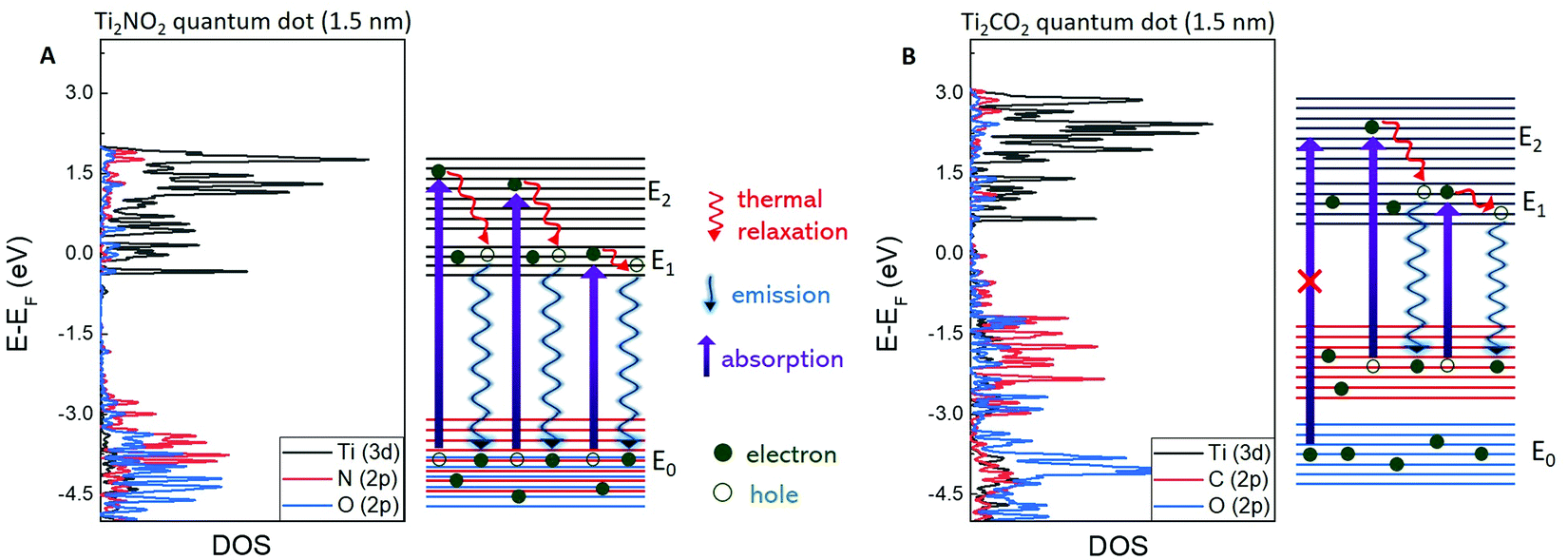 | ||
| Fig. 4 DFT calculation results of 1.5 nm Ti2NO2 (A) and Ti2CO2 (B) MQDs. The valence band, conduction band, and higher-energy conduction band are denoted as E0, E1, and E2, respectively. | ||
One interesting feature of the Ti2NO2 quantum dots is the high PLE at high-energy excitation (5.4 eV) which is absent in Ti2CO2. To understand this feature, we further investigated the DOS of Ti2CO2. Three main differences in the DOS between Ti2NTx and Ti2CTx were observed. First, the Fermi level in Ti2NO2 was located inside E1, whereas it was in the gap between E0 and E1 in Ti2CO2. Second, the bandgap between E0 and E1 of Ti2NO2 was 0.5 eV larger than that of Ti2CO2. Third, the DOS of N (2p) and O (2p) states in Ti2NO2 were strongly merged, inducing a strong absorption from E0 to both E1 and E2 at 3.8 and 5.4 eV, respectively. In contrast, the DOS of the C (2p) and O (2p) states in Ti2CO2 (Fig. 4B) were weakly merged and more dispersed over a large energy range. Consequently, the absorption from C (2p) to E1 and E2 (Ti (3d)) may appear at 3.3 and 4.3 eV, respectively, rather than in a higher energy range from O (2p) to E1 and E2, explaining the absence of PLE at energies higher than 4 eV in Ti2CO2. Further symmetry analysis for the selection rules should be performed to clarify this scenario.
4. Conclusions
We fabricated light-emitting Ti2N MQDs that were water-soluble with a QY of 7.5%. TEM and AFM analyses showed that the MQDs maintained the crystal structure of the MXene and had an average diameter of 3.14 nm. The PLE and excitation energy-dependent PL measurements suggested that the bandgap was 3.8 eV and that the deep-UV absorption originated from the electronic transition to the higher-lying conduction band (E2). The optical properties of the nitride MQDs were compared with those of the carbide MQDs. Nitride MQDs exhibited more efficient UV absorption and emitted PL with higher energy excitation. DFT calculations of DOS confirmed the band structure suggested by the optical measurements. Our progress in the fabrication of light-emitting MQDs with a nitride-based MXene and improved understanding of the origin of light emission will expand the application of MQDs in optoelectronic devices.Conflicts of interest
The authors declare no competing financial interests.Acknowledgements
J. K. acknowledges the support of the National Research Foundation of Korea (NRF), funded by the Ministry of Education (2021R1A6A1A03039696 and 2022R1A2C2009412). D. L. D. acknowledges the Institute for Basic Science (IBS-R011-D1) and Advanced Facility Center for Quantum Technology.Notes and references
- M. Naguib, M. Kurtoglu, V. Presser, J. Lu, J. Niu, M. Heon, L. Hultman, Y. Gogotsi and M. W. Barsoum, Adv. Mater., 2011, 23, 4248–4253 CrossRef CAS PubMed
.
- M. Naguib, R. R. Unocic, B. L. Armstrong and J. Nanda, Dalton Trans., 2015, 44, 9353–9358 RSC
- P. Urbankowski, B. Anasori, T. Makaryan, D. Er, S. Kota, P. L. Walsh, M. Zhao, V. B. Shenoy, M. W. Barsoum and Y. Gogotsi, Nanoscale, 2016, 8, 11385–11391 RSC
- T. Zhang, L. Pan, H. Tang, F. Du, Y. Guo, T. Qiu and J. Yang, J. Alloys Compd., 2017, 695, 818–826 CrossRef CAS
- B. Soundiraraju and B. K. George, ACS Nano, 2017, 11, 8892–8900 CrossRef CAS PubMed
- K. Hantanasirisakul and Y. Gogotsi, Adv. Mater., 2018, 30, e1804779 CrossRef PubMed
- K. Chaudhuri, M. Alhabeb, Z. Wang, V. M. Shalaev, Y. Gogotsi and A. Boltasseva, ACS Photonics, 2018, 5, 1115–1122 CrossRef CAS
- J. Cui, Q. Peng, J. Zhou and Z. Sun, Nanotechnology, 2019, 30, 345205 CrossRef CAS PubMed
- Y. Dong, Z. S. Wu, S. Zheng, X. Wang, J. Qin, S. Wang, X. Shi and X. Bao, ACS Nano, 2017, 11, 4792–4800 CrossRef CAS PubMed
- Q. Yang, W. Gao, W. Zhong, M. Tao, Y. Qi, S. J. Bao and M. Xu, New J. Chem., 2020, 44, 3072–3077 RSC
- M. Naguib, M. W. Barsoum and Y. Gogotsi, Adv. Mater., 2021, 33, 2103393 CrossRef CAS PubMed
- M. Naguib, V. N. Mochalin, M. W. Barsoum and Y. Gogotsi, Adv. Mater., 2014, 26, 992–1005 CrossRef CAS PubMed
- Q. Xue, H. Zhang, M. Zhu, Z. Pei, H. Li, Z. Wang, Y. Huang, Y. Huang, Q. Deng, J. Zhou, S. Du, Q. Huang and C. Zhi, Adv. Mater., 2017, 29, 1604847 CrossRef PubMed
- H. An, T. Habib, S. Shah, H. Gao, M. Radovic, M. J. Green and J. L. Lutkenhaus, Sci. Adv., 2018, 4, eaaq0118 CrossRef PubMed
- X. Jiang, A. V. Kuklin, A. Baev, Y. Ge, H. Ågren, H. Zhang and P. N. Prasad, Phys. Rep., 2020, 848, 1–58 CrossRef CAS
- E. Satheeshkumar, T. Makaryan, A. Melikyan, H. Minassian, Y. Gogotsi and M. Yoshimura, Sci. Rep., 2016, 6, 32049 CrossRef CAS PubMed
- Q. Xu, L. Ding, Y. Wen, W. Yang, H. Zhou, X. Chen, J. Street, A. Zhou, W.-J. Ong and N. Li, J. Mater. Chem. C, 2018, 6, 6360–6369 RSC
- X. Chen, X. Sun, W. Xu, G. Pan, D. Zhou, J. Zhu, H. Wang, X. Bai, B. Dong and H. Song, Nanoscale, 2018, 10, 1111–1118 RSC
- M. Liu, J. Zhou, Y. He, Z. Cai, Y. Ge, J. Zhou and G. Song, Mikrochim. Acta, 2019, 186, 770 CrossRef CAS PubMed
- A. Rafieerad, W. Yan, G. L. Sequiera, N. Sareen, E. Abu-El-Rub, M. Moudgil and S. Dhingra, Adv. Healthcare Mater., 2019, 8, 1900569 CrossRef PubMed
- G. Cai, Z. Yu, P. Tong and D. Tang, Nanoscale, 2019, 11, 15659–15667 RSC
- Q. Guan, J. Ma, W. Yang, R. Zhang, X. Zhang, X. Dong, Y. Fan, L. Cai, Y. Cao, Y. Zhang, N. Li and Q. Xu, Nanoscale, 2019, 11, 14123–14133 RSC
- J. Shao, J. Zhang, C. Jiang, J. Lin and P. Huang, Chem. Eng. J., 2020, 400, 126009 CrossRef CAS
- Y. Li, L. Ding, Y. Guo, Z. Liang, H. Cui and J. Tian, ACS Appl. Mater. Interfaces, 2019, 11, 41440–41447 CrossRef CAS PubMed
- Q. Xu, W. Yang, Y. Wen, S. Liu, Z. Liu, W. J. Ong and N. Li, Appl. Mater. Today, 2019, 16, 90–101 CrossRef
- X. Chen, J. Li, G. Pan, W. Xu, J. Zhu, D. Zhou, D. Li, C. Chen, G. Lu and H. Song, Sens. Actuators, B, 2019, 289, 131–137 CrossRef CAS
- M. L. Desai, H. Basu, R. K. Singhal, S. Saha and S. K. Kailasa, Colloids Surf., A, 2019, 565, 70–77 CrossRef CAS
- B. Shao, Z. Liu, G. Zeng, H. Wang, Q. Liang, Q. He, M. Cheng, C. Zhou, L. Jiang and B. Song, J. Mater. Chem. A, 2020, 8, 7508–7535 RSC
- Q. Zhang, Y. Sun, M. Liu and Y. Liu, Nanoscale, 2020, 12, 1826–1832 RSC
- A. S. Sharbirin, S. Akhtar and J. Kim, Opto-Electronic Adv., 2021, 4, 20007701–20007715 Search PubMed
- X. Yu, X. Cai, H. Cui, S. W. Lee, X. F. Yu and B. Liu, Nanoscale, 2017, 9, 17859–17864 RSC
- W. Dai, H. Dong and X. Zhang, Materials, 2018, 11, 1776 CrossRef PubMed
- S. Lu, L. Sui, Y. Liu, X. Yong, G. Xiao, K. Yuan, Z. Liu, B. Liu, B. Zou and B. Yang, Adv. Sci., 2019, 6, 1801470 CrossRef PubMed
- Q. Xu, J. Ma, W. Khan, X. Zeng, N. Li, Y. Cao, X. Zhao and M. Xu, Chem. Commun., 2020, 56, 6648–6651 RSC
- D. Huang, Y. Xie, D. Lu, Z. Wang, J. Wang, H. Yu and H. Zhang, Adv. Mater., 2019, 31, 1901117 CrossRef PubMed
- S. Roy, A. S. Sharbirin, Y. Lee, W. Bin Kim, T. S. Kim, K. Cho, K. Kang, H. S. Jung and J. Kim, Nanomaterials, 2020, 10, 1032 CrossRef CAS PubMed
- J. Sheng, U. Welzel and E. J. Mittemeijer, Appl. Phys. Lett., 2010, 97, 95–98 CrossRef
- J. Gou, L. Zhao, Y. Li and J. Zhang, ACS Appl. Nano Mater., 2021, 4, 12308–12315 CrossRef CAS
- P. Vaqueiro and M. A. López-Quintela, J. Mater. Chem., 1998, 8, 161–163 RSC
- D. Schroeer and R. C. J. Nininger, Phys. Rev. Lett., 1967, 19, 1966–1968 CrossRef
- Y. Xu, X. Wang, W. L. Zhang, F. Lv and S. Guo, Chem. Soc. Rev., 2018, 47, 586–625 RSC
- S. Roy, G. P. Neupane, K. P. Dhakal, J. Lee, S. J. Yun, G. H. Han and J. Kim, J. Phys. Chem. C, 2017, 121, 1997–2007 CrossRef CAS
- R. M. Al Mohaimeed, A. A. Ansari and A. Aldwayyan, J. Spectrosc., 2018, 2018, 1–9 CrossRef
- T. E. Saraswati, U. H. Setiawan, M. R. Ihsan, I. Isnaeni and Y. Herbani, Open Chem., 2019, 17, 1198–1212 CAS
- Q. Xu, L. Ding, Y. Wen, W. Yang, H. Zhou, X. Chen, J. Street, A. Zhou, W.-J. Ong and N. Li, J. Mater. Chem. C, 2018, 6, 6360–6369 RSC
- Y. Wang and A. Hu, J. Mater. Chem. C, 2014, 2, 6921–6939 RSC
- B. O. Dabbousi, J. Rodriguez-Viejo, F. V. Mikulec, J. R. Heine, H. Mattoussi, R. Ober, K. F. Jensen and M. G. Bawendi, J. Phys. Chem. B, 1997, 101, 9463–9475 CrossRef CAS
-
J. E. Pelayo-Ceja, A. Zazueta-Raynaud, R. Lopez-Delgado, E. Saucedo-Flores, R. Ruelas-Lepe, F. Orona-Magallanes, R. Guerrero-Gonzalez and A. Ayon, 2018 Symposium on Design, Test, Integration & Packaging of MEMS and MOEMS (DTIP), IEEE, 2018, pp. 1–4 Search PubMed
Footnote |
| † Electronic supplementary information (ESI) available: TEM image of Ti2C MQDs (S1); fluorescence of Ti2N MQDs dispersed in water (S2); PL spectrum of Ti2N MQD solution and thin film under 375 nm laser excitation. Confocal image of thin-film Ti2N MQDs under 405 nm laser excitation. Thin-film Ti2N MQDs drop-casted on a quartz substrate illuminated with an UV (250 nm) LED (S3); plot of Ti2N MQDs’ QY (%) estimation vs. excitation energy (S4); PL intensity and QY of Ti2N MQDs in 10 days (S5); PL spectra and QY of Ti2N MQDs at different pH values ranging from 2 to 12 (S6); UV-Vis absorption spectra, PL spectra and QY of Ti2N MQDs in the presence of Co2+ and Mn2+ ions (S7); DFT calculation of Ti2NO2 MQDs with sizes of 1.5 nm and 3 nm (S8); DFT calculation of Ti2N MQDs (S9). See https://doi.org/10.1039/d2tc00568a |
| This journal is © The Royal Society of Chemistry 2022 |