
An asymmetric A–DA′D–π-A type non-fullerene acceptor for high-performance organic solar cells†
Zhe
Zhang‡
a,
Dawei
Li‡
a,
Huarui
Zhang
b,
Xueqin
Ma
b,
Ya-Nan
Chen
c,
Andong
Zhang
c,
Xiaoyun
Xu
d,
Yahui
Liu
*c,
Zaifei
Ma
 d and
Zhishan
Bo
*bc
d and
Zhishan
Bo
*bc
aKey Laboratory of Eco-functional Polymer Materials of the Ministry of Education, Key Laboratory of Eco-environmental Polymer Materials of Gansu Province, College of Chemistry and Chemical Engineering, Northwest Normal University, Lanzhou 730070, China
bBeijing Key Laboratory of Energy Conversion and Storage Materials, College of Chemistry, Beijing Normal University, Beijing 100875, China. E-mail: zsbo@bnu.edu.cn
cCollege of Textiles & Clothing, Qingdao University, Qingdao 266071, China. E-mail: liuyh@qdu.edu.cn
dCenter for Advanced Low-Dimension Materials, State Key Laboratory for Modification of Chemical Fibers and Polymer Materials, College of Materials Science and Engineering, Donghua University, Shanghai 201620, China
First published on 17th November 2021
Abstract
Under the guidance of a symmetry-breaking and π-bridge-extending strategy, three asymmetric and symmetric non-fullerene acceptors (L1, L2, and L3) with DA′D core units and two 2-(5,6-difluoro-3-oxo-2,3-dihydro-1H-inden-1-ylidene)malononitrile electron-withdrawing units (A) have been designed and synthesized via changing the alkoxy-substituted thiophene bridge unit. The asymmetric A–DA′D–π-A-type non-fullerene acceptor (NFA) L2 displays much improved solubility and a slightly larger molar absorption coefficient than its symmetric counterparts (L1 and L3). In addition, blend film based on the asymmetric NFA L2 shows suitable nanoscale phase morphology and much higher and more balanced hole and electron mobilities. Hence, compared with L1- and L3-based organic solar cells (OSCs), optimal L2-based devices can deliver a high power-conversion efficiency (PCE) of 14.06% with simultaneously enhanced current density and fill factor values. Our study indicates that a combined symmetry-breaking and π-bridge-extending strategy is powerful for the design of high-performance NFAs.
Introduction
Organic solar cells (OSCs) have attracted much attention during the past several years due to their intrinsic advantages, such as being lightweight and flexible, having roll-to-roll processing capacity, etc.1–6 In the past several decades, fullerene-derivative acceptors have become prevalent in the field of OSCs. However, the inherent drawbacks of fullerene derivatives, such as their narrow and weak absorption, nonadjustable energy levels, poor stability, etc., have limited further improvements in the photovoltaic performances of OSCs. By 2016, the power conversion efficiencies (PCEs) of OSCs had reached a bottleneck of approximately 11%. However, in recent years, researchers have focused on alternative acceptors, so-called non-fullerene acceptors (NFAs), promoting the rapid development of OSCs. Nowadays, the PCEs of single-junction OSCs have reached over 18%,7,8 demonstrating great potential for commercial applications.Typical high-performance NFAs have A–D–A-type molecular configurations, which usually consist of three parts:9–12 a large planar electron-donating multi-fused-ring core unit (D); electron-withdrawing terminal groups (A); and out-of-plane side chains. The insertion of a π-bridge unit between the D and A units is a possible way to reduce the size of the central core unit. The introduction of a π-bridge unit has many advantages, such as reducing the synthetic complexity, adjusting the molecular planarity, regulating the crystallinity of acceptors, facilitating π-electron delocalization, enhancing the charge transport capacity, and, finally, improving the photovoltaic performance. A large number of high-performance A–π-D–π-A acceptors have been reported.13–15
Recently, Zou et al. reported a series of high-performance NFAs with A–DA′D–A-type molecular structures, termed Y-series acceptors.16 These acceptors further promoted the photovoltaic performances of OSCs. Compared with typical A–D–A-type acceptors (like ITIC and IT-4F), the fused DA′D central core with two pyrrole rings and “V”-shaped molecular geometry leads to Y-series acceptors with more π–π stacking possibilities, stronger near-infrared absorption, and larger photoluminescence quantum yields.10,17–20
Since we reported the first fused-ring acceptors with asymmetric side chains, symmetry-breaking strategies have drawn a lot of attention in the design of fused-ring acceptors.21 Various asymmetric acceptors with asymmetric core units, asymmetric side chains, and asymmetric terminal groups have been developed. Asymmetric molecular design can regulate the dipole moment, solubility, electron mobility, absorption spectrum, crystallization behaviour, etc.22–28 State-of-the-art devices based on asymmetric acceptors have achieved power conversion efficiencies (PCEs) of over 17%.29–31 However, integrated investigations involving symmetry breaking, π-bridge extension, and A–DA′D–A structures are still rare.32
Inspired by the above-mentioned knowledge, symmetric and asymmetric NFAs (L1, L2, and L3), as shown in Chart 1, with DA′D cores and 2-(5,6-difluoro-3-oxo-2,3-dihydro-1H-inden-1-ylidene)malononitrile electron-withdrawing units (A) are designed and synthesized via regulating the alkoxy-substituted thiophene bridge unit. Unexpectedly, the asymmetric acceptor L2 displays much higher solubility than the two symmetric acceptors (L1 and L3). The molar absorption coefficient of L2 is also slightly larger than those of L1 and L3. Unlike L3, which adopts a dominant edge-on molecular orientation, L2 has a dominant face-on molecular orientation in neat film. As expected, L2-based blend film exhibits appropriate nanoscale phase separation, with high and balanced hole and electron mobilities. By comparison, L1-based blend film displays very low hole and electron mobilities, and L3-based blend film exhibits very large phase separation. Finally, OSCs based on the asymmetric acceptor L2 can deliver an excellent PCE of 14.06%, with a high short-circuit current (Jsc) of 24.01 mA cm−2 and a fill factor (FF) of 71.73%, much higher than the PCEs of OSCs based on the symmetric acceptors L1 (2.07%) and L3 (1.78%). With a combination of symmetry breaking, π-bridge extension, and the use of an A–DA′D–A structure, our results provide a new molecular design strategy for high-performance NFAs.
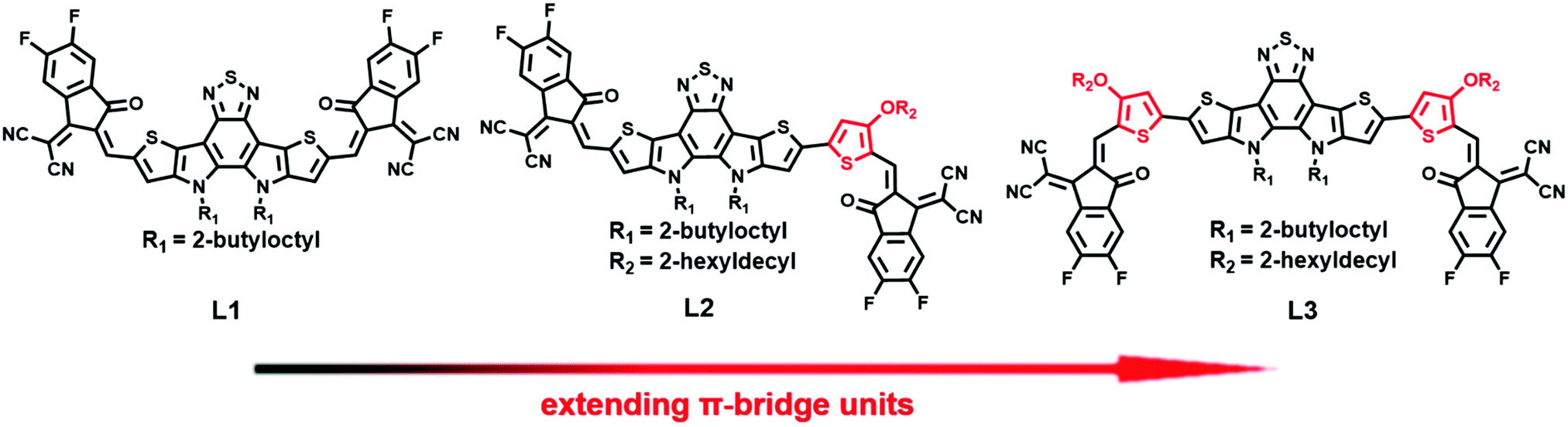 | ||
| Chart 1 The chemical structures of L1, L2, and L3. | ||
Results and discussion
The chemical structures of L1, L2, and L3 are shown in Chart 1, the synthetic routes to L2 and L3 are described in Scheme 1, and detailed procedures are provided in the ESI.† The starting material (compound 1) and small molecule acceptor (L1) were prepared based on the previous literature.33 The bromination of compound 1 with NBS gave a mixture of compounds 2 and 3, which can be used for the next step without purification. Stille coupling of this mixture (2 and 3) and (4-((2-hexyldecyl)oxy)thiophen-2-yl)trimethylstannane with Pd(PPh3)4 as the catalyst precursor afforded a mixture of intermediates (4 and 5).34 Subsequently, the Vilsmeier–Haack reaction was employed to furnish compounds 6 and 7, which can be easily separated via column chromatography. The target acceptors (L2 and L3) were synthesized via the Knoevenagel condensation of the dialdehyde intermediates (6 and 7) with 2-(5,6-difluoro-3-oxo-2,3-dihydro-1H-inden-1-ylidene)malononitrile, resulting in yields of 70% and 60%, respectively. 1H- and 13C-NMR spectroscopy and high-resolution mass spectrometry were used to verify the chemical structures of these acceptors. Furthermore, the solubilities of L1, L2, and L3 in chlorobenzene were estimated to be 20.50, 52.90, and 13.84 mg mL−1, respectively. Obviously, the asymmetric acceptor (L2) displays much better solubility than its symmetric counterparts (L1 and L3). It is well known that good solubility is favourable for achieving better active layer morphology when blending with a donor polymer.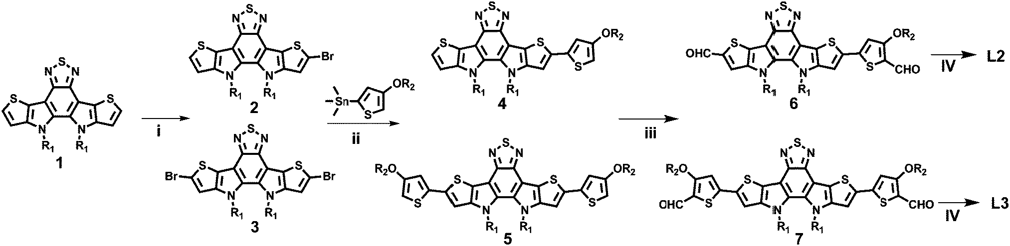 | ||
| Scheme 1 Synthetic routes to L2 and L3. (i) NBS, THF, 0 °C; (ii) (4-((2-hexyldecyl)oxy)thiophen-2-yl)trimethylstannane, Pd(PPh3)4, toluene, reflux; (iii) POCl3, 1,2-dichloroethane, DMF, 80 °C; (iv) 2-(5,6-difluoro-3-oxo-2,3-dihydro-1H-inden-1-ylidene)malononitrile, pyridine, CHCl3, rt. | ||
The UV-vis absorption behaviours of L1, L2, and L3 in dilute chloroform solutions and as thin films were investigated, and spectra are shown in Fig. 1. In solution form, L1, L2, and L3 display a broad absorption band, with the maximum absorption peaks located at 697, 724, and 738 nm, respectively. It can be found that the absorption peak is obviously redshifted upon increasing the conjugation length. The asymmetric acceptor L2 exhibits the largest molar absorption coefficient (1.7 × 10⁵ M−1 cm−1) among these three acceptors (L1: 1.56 × 10⁵ M−1 cm−1; and L3: 1.56 × 10⁵ M−1 cm−1). In going from solution to thin film, the absorption spectra of these acceptors are all redshifted, with two clear absorption peaks, indicating strong aggregation in the solid state. The maximum absorption peaks of L1, L2, and L3 in thin-film form are located at 746, 776, and 814 nm, respectively. The optical bandgaps (Eoptg) of L1, L2, and L3 are calculated to be 1.49, 1.45, and 1.42 eV from the onset of film absorption based on the equation: Eoptg =1240/λedge. Cyclic voltammetry (CV) measurements were used to estimate the energy levels of the acceptors. The highest occupied molecular orbital (HOMO) and lowest unoccupied molecular orbital (LUMO) energy levels can be calculated based on the equation: EHOMO/LUMO = −e(Eox/red − E(Fc/Fc+) + 4.8) (eV). As shown in Fig. 2, the HOMO/LUMO energy levels were determined to be −5.68/−3.79 eV for L1, −5.56/−3.88 eV for L2, and −5.38/−3.87 eV for L3. The introduction of π-bridge units can significantly lift the HOMO energy levels due to electron-donating features. In addition, the detailed electrochemical and optical properties are summarized in Table 1.
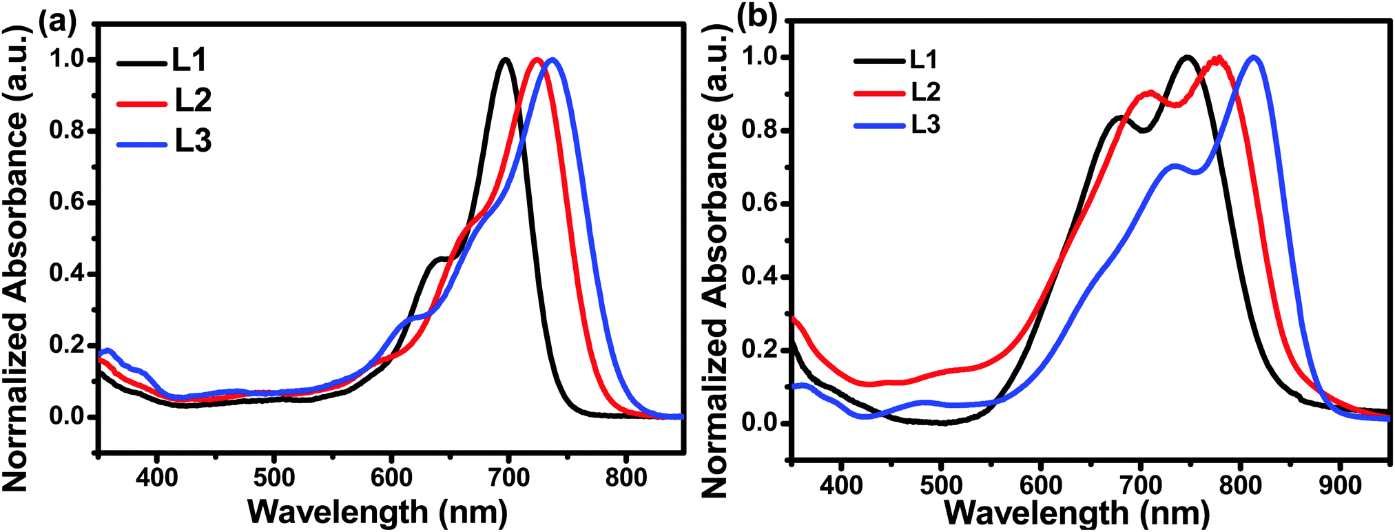 | ||
| Fig. 1 UV-Vis absorption spectra of L1, L2, and L3 in CHCl3 solutions (a) and as thin films (b). | ||
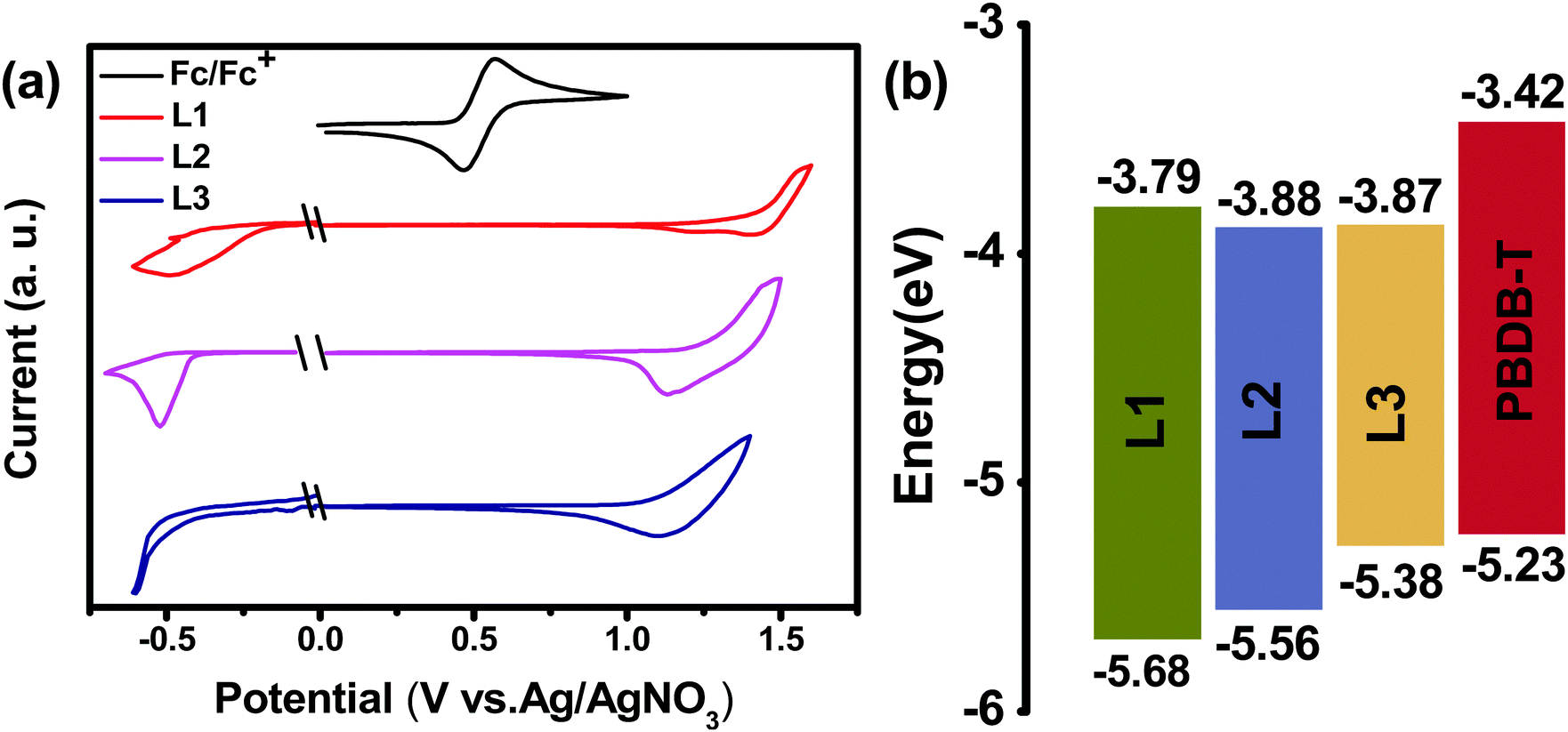 | ||
| Fig. 2 (a) The electrochemical properties of L1, L2, and L3 from cyclic voltammetry. (b) An energy band diagram showing the acceptor and donor HOMO/LUMO positions. | ||
The molecular geometries and energy levels of these three acceptors were investigated based on density functional theory (DFT) calculations at the B3LYP/6-31G(d) level. The alkyl and alkoxyl side chains were simplified to methyl and methoxy to reduce the complexity of calculations. The calculated molecular conformations, HOMO/LUMO wave function distributions, and energy levels are shown in the ESI.† These three acceptors all display planar molecular geometries, which is beneficial for electron delocalization. The electron clouds of the HOMOs and LUMOs are uniformly distributed along the molecular backbones of the acceptors. The theoretical LUMO/HOMO energy levels are determined to be −3.93/−6.06 eV for L1, −3.77/−5.81 eV for L2, and −3.62/−5.63 eV for L3, which is consistent with the CV measurements.
The photovoltaic performances of L1, L2, and L3 can be evaluated using inverted devices with an ITO/ZnO/polymer:acceptor/MoO3/Ag configuration, where commonly used PBDB-T was chosen as the donor polymer due to its complementary absorption and matched energy levels with these acceptors. The ZnO layer was prepared according to a procedure in the literature.35 The synthesis conditions, such as the polymer concentration, active layer composition, spin-coating rate, and additive, are systematically optimized. The detailed optimization process is described in the ESI.† As shown in Fig. 3 and Table 2, the device based on the asymmetric acceptor L2 exhibits the highest PCE of 14.06%, with an open-circuit voltage (Voc,) of 0.82 V, a short-circuit current (Jsc) of 24.01 mA cm−2, and a fill factor (FF) of 71.73%, which is much higher than the PCEs of OSCs based on the symmetric acceptors L1 (2.07%) and L3 (1.78%). It is obvious that small structural variations in the acceptor molecules caused huge differences in device performance. The main reason for the very low power conversion efficiency of the device based on L1 is probably its extremely low charge mobility, whereas the low efficiency of the device based on L3 is probably caused by its poor blend film morphology (vide infra). With an increase in the conjugation length, the Voc values of the devices increased from 0.69 V for L1 to 0.82 V for L2 to 0.91 V for L3. External quantum efficiency (EQE) measurements are used to verify the accuracy of the Jsc values obtained from J–V curves. As shown in Fig. 3, L2-based devices possess the best photo-to-current response among these three acceptors, and the maximum EQE value approaches approximately 80%, which is consistent with the J–V curve results. To reveal the reasons behind the huge device performance differences between these three acceptors, detailed characterization, including morphology, charge mobility, charge recombination behavior, and energy loss analysis, of the devices was carried out (vide infra). Moreover, the stability of the L2-based device arrangement is also measured. As shown in the ESI,† the PCE of an L2-based device maintains 86% of its initial value after being placed in a glove box for 168 h, which implies the good stability of the asymmetric acceptor.
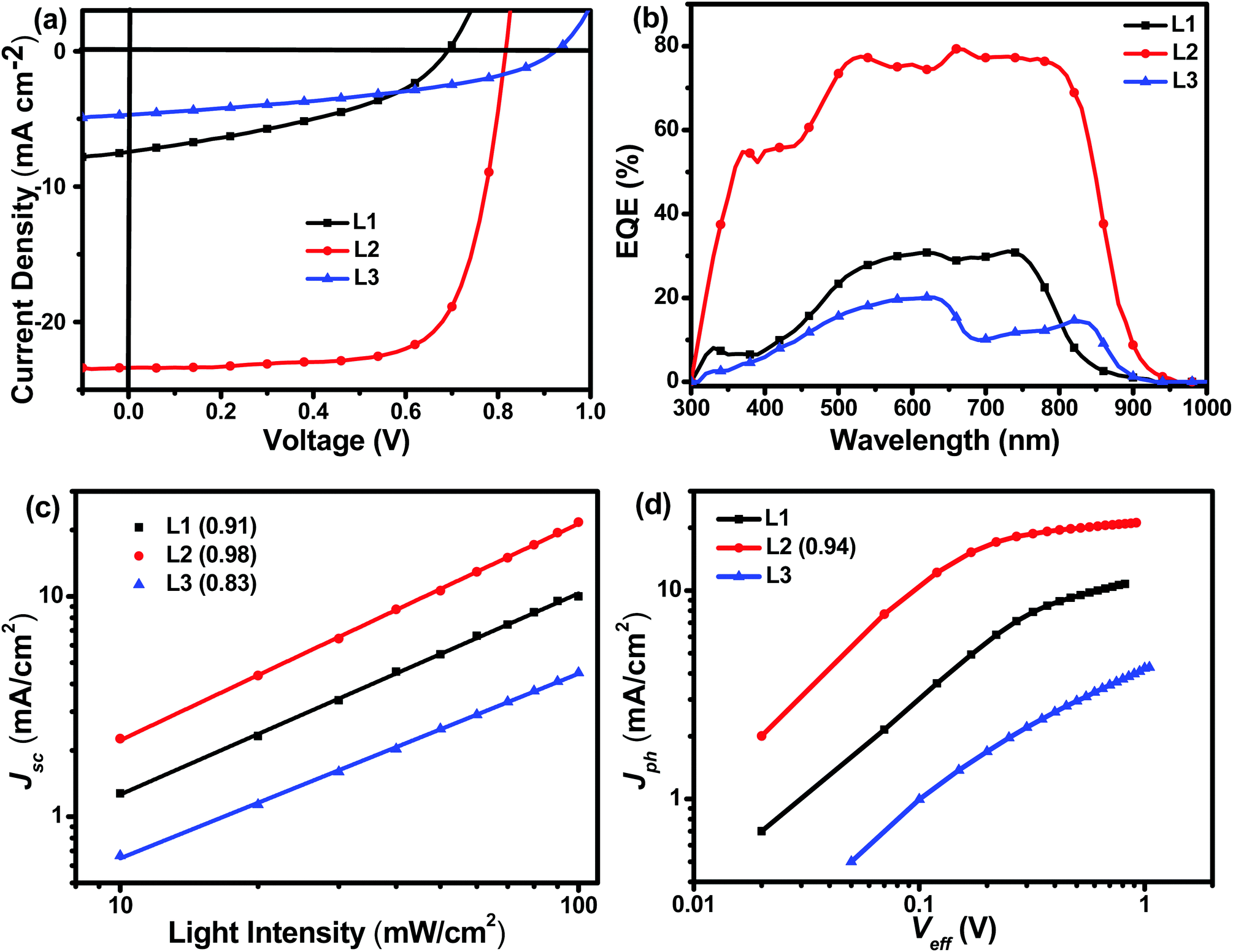 | ||
| Fig. 3 (a) J–V and (b) EQE curves of L1-, L2-, and L3-based devices, (c) the dependence of Jsc on Plight, and (d) the dependence of Jph on Veff. | ||
A systematic investigation of the charge recombination behaviour can provide better understanding of the significant difference in FF values between OSCs based on L1, L2, and L3. The relationship between Jsc and light intensity (Plight) can be described as Jsc ∝ Plightα, in which α is an exponential factor representing bimolecular recombination. As shown in Fig. 3, Jsc and Plight were plotted in a log–log plot. The α values of the L1- and L3-based devices are 0.91 and 0.83, respectively, much lower than that of a device based on L2 (0.98). Typically speaking, a higher α value, especially approaching 1, means more efficient photogenerated exciton transport and much reduced geminate recombination loss, which is beneficial for achieving a higher FF.36 Therefore, Jscvs. Plight measurements can explain well why the L2-based device has the highest FF among these three acceptors. Further, the photocurrent density (Jph) and effective voltage (Veff) are also measured and used to reveal the charge recombination processes in the OSCs. Using the equation Jph = JL − JD, Jph can be calculated, where JL and JD represent the photocurrent densities under light and in the dark, respectively. Similarly, in the equation Veff = Vo − V, Vo represents the voltage when JL = JD, and V is the applied voltage. As shown in Fig. 3, L1- and L3-based OSCs cannot achieve saturated photocurrent density (Jsat) even when Veff approaches 1, indicating serious charge recombination in the devices. In comparison, L2-based devices reach Jsat with a Jph/Jsat ratio of 0.94, indicating efficient exciton dissociation and suppressed charge recombination. All in all, these charge recombination behaviour investigations can reveal well the reasons for the much higher FF of L2-based devices than L1- and L3-based ones.
Energy loss (Eloss) analysis is conducted based on highly sensitive external quantum efficiency (sEQE) and electroluminescence (EL) measurements to understand the Voc differences between OSCs based on these different acceptors. Eloss can be calculated based on the equation Eloss = Eg − qVoc, where Eg is the corresponding cross-point of UV-vis and photoluminescence (PL) spectra.37 As shown in Table 3, L1-, L2-, and L3-based devices display Eloss values of 0.85, 0.68, and 0.55 eV, respectively. As shown in Fig. 4, the charge transfer state energy (Ect) of the blend films can be estimated based on the cross-point of Gaussian fitting curves of the sEQE and EL curves. Accordingly, the Ect values of L1-, L2-, and L3-based devices are 1.29, 1.36, and 1.39 eV, respectively. The tendencies of the Eloss and Ect variations can explain the Voc trend; that is, the higher Ect and lower Eloss values of the L3-based device result in it showing the highest Voc value among the devices based on these three acceptors. Furthermore, the energy loss of OSCs can be divided into three parts: radiative energy loss (ΔE1), charge generation energy loss (ΔE2), and nonradiative energy loss (ΔE3).38–40 The ΔE2 values, the difference between Eg and Ect, of L1-, L2-, and L3-based devices are 0.25, 0.13, and 0.08 eV. ΔE3 can be determined according to the equation ΔE3 = kBT/qln(1/EQEEL), where kB, T, and q represent the Boltzmann constant, temperature, and elementary charge, respectively. The ΔE3 values of L1-, L2-, and L3-based devices are 0.32, 0.27, and 0.20 eV, respectively. Finally, the ΔE1 values, defined via removing ΔE2 and ΔE3 from Eloss, of L1-, L2-, and L3-based devices are 0.28, 0.28, and 0.27 eV, respectively. Above all, the asymmetric L2-based device displays medium energy loss. Our results demonstrate that asymmetric molecular design can achieve a balance between energy loss and photovoltaic performance.
| Active layer | E g [eV] | E ct [eV] | EQEEL [%] | E loss [eV] | ΔE1 [eV] | ΔE2 [eV] | ΔE3 [eV] |
|---|---|---|---|---|---|---|---|
| PBDB-T:L1 | 1.54 | 1.29 | 1.13 × 10⁻⁴ | 0.85 | 0.28 | 0.25 | 0.32 |
| PBDB-T:L2 | 1.49 | 1.36 | 6.99 × 10⁻⁴ | 0.68 | 0.28 | 0.13 | 0.27 |
| PBDB-T:L3 | 1.47 | 1.39 | 2.61 × 10⁻² | 0.55 | 0.27 | 0.08 | 0.20 |
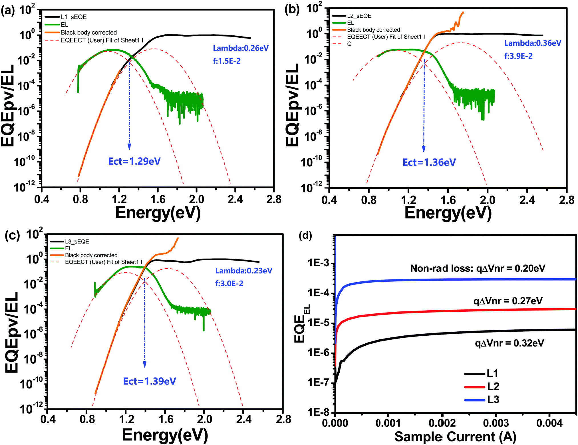 | ||
| Fig. 4 Normalized sEQE spectra of solar cells based on L1 (a), L2 (b), and L3 (c), and EL curves (d). | ||
The blend film morphologies are investigated via atomic force microscopy (AFM) and transmission electron microscopy (TEM) to understand the photovoltaic performances of the OSCs based on these acceptors. As shown in Fig. 5, AFM images of blend films based on PBDB-T:L1 and PBDB-T:L2 show homogeneous surface morphologies without apparent large-scale phase separation, while the blend film based on PBDB-T:L3 shows large-scale phase separation. The root-mean-square (RMS) roughness values of 2.11 nm for PBDB-T:L1, 1.48 nm for PBDB-T:L2, and 5.65 nm for PBDB-T:L3 are obtained from AFM height images. Obviously, L2-based blend film has a more homogenous phase morphology, with the lowest RMS value. In addition, the TEM results are consistent with the AFM measurements. PBDB-T:L3 blend film displays apparent larger-scale phase separation, with large dark and light regions, which are more obvious in the inset of Fig. 5f. As for PBDB-T:L1 blend film, moderate phase separation morphology is seen, with sparse and burly fibrils. PBDB-T:L2 blend film exhibits appropriate phase separation, with fibrils having diameters of 10 to 20 nm, which is beneficial for charge transport, thus leading to the high Jsc and FF values of related OSCs. We speculate that the reason for the formation of different morphologies is the varied solubilities of acceptors. More specifically speaking, the asymmetric acceptor L2 possesses the best solubility among these acceptors (vide supra), which can delay precipitation during the film-deposition process, thus, better film morphology can be formed.41 To investigate the charge-transport properties of the devices, the space-charge limited current (SCLC) method was utilized to estimate the hole (μh) and electron (μe) transport mobilities based on typical device configurations of ITO/PEDOT:PSS/active layer/Au and ITO/ZnO/active layer/Al, respectively. As shown in the ESI,† PBDB-T:L1 blend film displays inferior μh and μe values of 7.57 × 10⁻⁶ cm2 V−1 s−1 and 1.47× 10⁻⁶ cm2 V−1 s−1, respectively. For PBDB-T:L3 blend film, the μh and μe values are slightly higher, with values of 3.49 × 10⁻⁵ cm2 V−1 s−1 and 3.28 × 10⁻⁶ cm2 V−1 s−1, respectively. More impressively, PBDB-T:L2 blend film possesses the highest μh and μe values of 1.52 × 10⁻⁴ cm2 V−1 s−1 and 1.48 × 10⁻⁴ cm2 V−1 s−1, with a μh/μe ratio of 1.03. The significantly higher and more balanced hole and electron transport mobilities of the L2-based device can explain its superior Jsc and FF values, which lead to the observably higher photovoltaic performance out of these three acceptors.
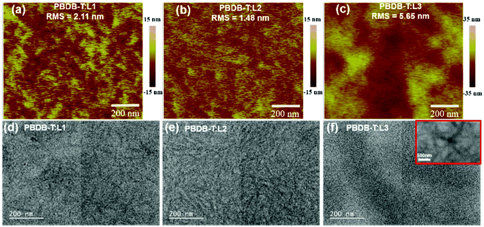 | ||
| Fig. 5 AFM and TEM images of PBDB-T:L1 film (a and d), PBDB-T:L2 film (b and e), and PBDB-T:L3 film (c and f). | ||
Grazing-incidence wide-angle X-ray scattering (GIWAXS) measurements are used to investigate molecular orientation and packing. As shown in Fig. 6, neat L1 and L2 films display an obvious (010) diffraction peak in the out-of-plane (OOP) direction and a (100) diffraction peak in the in-plane (IP) direction, indicating the formation of a predominantly face-on orientation. In particular, neat L2 film exhibits much stronger (010) diffraction, based on the 2D GIWAXS pattern and 1D profile, indicating the high crystallinity of L2. Conversely, a dominant edge-on molecular orientation is formed in neat L3 film, with observable (010) and (100) diffraction peaks in the IP and OOP directions, respectively. The π–π stacking distances of L1, L2, and L3 are quite similar, all about 3.50 Å. The lamellar stacking distance is gradually increased from L1 (17.44 Å) to L2 (18.48 Å) to L3 (19.63 Å), probably reflecting the molecular backbone lengths of the acceptors. Both L1 and L2 in blend films with PBDB-T adopt preferential face-on orientations. Also, the (010) diffraction of L2-based blend film is much stronger than that of the L1-based example. However, PBDB-T:L3 blend film displays mixed molecular orientations (face-on and edge-on) based on the 2D GIWAXS pattern and 1D profile. In addition, the crystal coherence length (CCL) is estimated to analyse the crystallinity quality.42,43 Based on the equation CCL = 2π/FWHM, the CCL values of the (010) diffraction peaks in the OOP direction were 21.83, 22.09, and 16.34 Å for PBDB-T:L1, PBDB-T:L2, and PBDB-T:L3 films, respectively, indicating that L2-based blend film has the best crystallinity quality.44 All in all, molecular orientation and stacking analysis can explain well the excellent photovoltaic performance of the L2-based device.
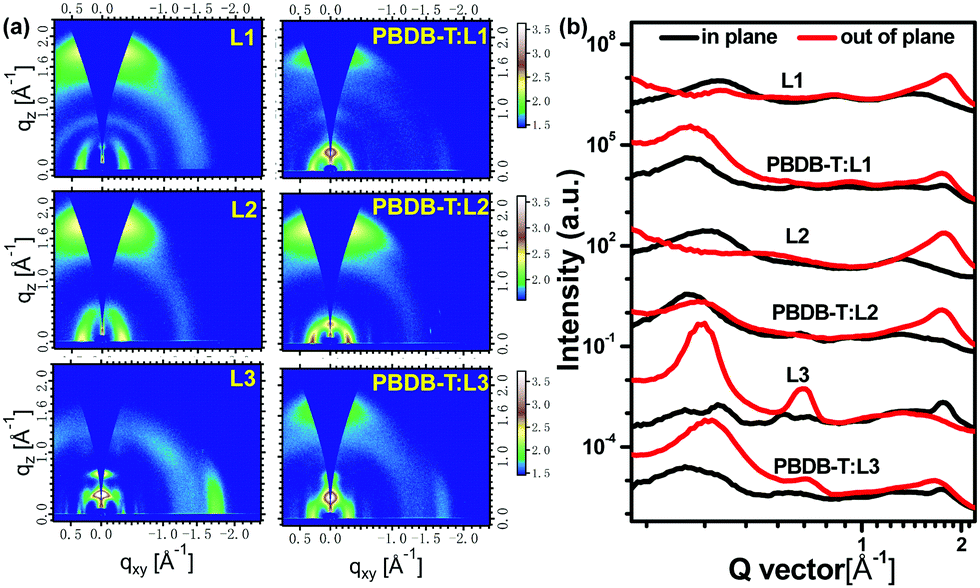 | ||
| Fig. 6 (a) 2D GIWAXS patterns and (b) 1D scattering profiles of neat L1, L2, and L3 films and corresponding blend films. | ||
Conclusions
In summary, three low-bandgap non-fullerene acceptors (L1, L2, and L3) are designed and synthesized via regulating the π-bridge units. Assisted by a symmetry-breaking strategy, the asymmetric acceptor L2, with one π-bridge thiophene unit, displays the best solubility among these three acceptors, which helps form appropriate phase morphology. In addition, L2 possesses a higher molar absorption coefficient in solution. In particular, asymmetric L2 and its corresponding blend film exhibit a predominantly face-on orientation and strong crystallinity, which can facilitate charge transport. As expected, much higher and more balanced hole and electron mobilities are achieved in L2-based devices. Hence, a high PCE of 14.06% is achieved in a device based on the asymmetric acceptor L2, which is much higher than those obtained using its symmetric counterparts (2.17% for L1 and 1.78% for L3). Device physics investigations reveal that L2-based devices exhibit low charge recombination and moderate energy loss. All in all, our work provides an effective way to fabricate high-performance non-fullerene acceptors via a symmetry-breaking strategy.Conflicts of interest
There are no conflicts to declare.Acknowledgements
The authors gratefully acknowledge financial support from the National Natural Science Foundation of China (51933001) and China Postdoctoral Science Foundation (2018M641033).Notes and references
- A. Armin, W. Li, O. J. Sandberg, Z. Xiao, L. Ding, J. Nelson, D. Neher, K. Vandewal, S. Shoaee, T. Wang, H. Ade, T. Heumüller, C. Brabec and P. Meredith, Adv. Energy Mater., 2021, 11, 20003570 CrossRef.
- K. Sreedhar Ram, H. Mehdizadeh-Rad, D. Ompong, D. D. Y. Setsoafia and J. Singh, Nanomaterials, 2021, 11, 209 CrossRef PubMed.
- Y. Un Kim, G. Eun Park, S. Choi, D. Hee Lee, M. Ju Cho and D. H. Choi, J. Mater. Chem. C, 2017, 5, 7182–7190 RSC.
- R. Li, G. Liu, R. Xie, Z. Wang, X. Yang, K. An, W. Zhong, X.-F. Jiang, L. Ying, F. Huang and Y. Cao, J. Mater. Chem. C, 2018, 6, 7046–7053 RSC.
- Y. Cui, H. Yao, L. Hong, T. Zhang, Y. Tang, B. Lin, K. Xian, B. Gao, C. An, P. Bi, W. Ma and J. Hou, Natl. Sci. Rev., 2020, 7, 1239–1246 CrossRef CAS.
- L. Huo, T. Liu, B. Fan, Z. Zhao, X. Sun, D. Wei, M. Yu, Y. Liu and Y. Sun, Adv. Mater., 2015, 27, 6969–6975 CrossRef CAS PubMed.
- Q. Liu, Y. Jiang, K. Jin, J. Qin, J. Xu, W. Li, J. Xiong, J. Liu, Z. Xiao, K. Sun, S. Yang, X. Zhang and L. Ding, Sci. Bull., 2020, 65, 272–275 CrossRef CAS.
- Y. Cui, Y. Xu, H. Yao, P. Bi, L. Hong, J. Zhang, Y. Zu, T. Zhang, J. Qin, J. Ren, Z. Chen, C. He, X. Hao, Z. Wei and J. Hou, Adv. Mater., 2021, 33, 2102420 CrossRef CAS PubMed.
- Z. Liu, X. Zhang, P. Li and X. Gao, Sol. Energy, 2018, 174, 171–188 CrossRef CAS.
- J. Miao, B. Meng, J. Liu and L. Wang, Chem. Commun., 2018, 54, 303–306 RSC.
- K. Jin, C. Deng, L. Zhang, D. Li, T. Li, F. Wang, Y. Yuan, Z. Xiao and L. Ding, Mater. Chem. Front., 2018, 2, 1716–1719 RSC.
- Y.-N. Chen, R. Zheng, J. Wang, H. Wang, M. Li, Y. Wang, H. Lu, Z. Zhang, Y. Liu, Z. Tang and Z. Bo, J. Mater. Chem. C, 2021, 9, 6937–6943 RSC.
- Y. Liu, C. e. Zhang, D. Hao, Z. Zhang, L. Wu, M. Li, S. Feng, X. Xu, F. Liu, X. Chen and Z. Bo, Chem. Mater., 2018, 30, 4307–4312 CrossRef CAS.
- C. He, Y. Li, Y. Liu, Y. Li, G. Zhou, S. Li, H. Zhu, X. Lu, F. Zhang, C.-Z. Li and H. Chen, J. Mater. Chem. A, 2020, 8, 18154–18161 RSC.
- H. Yao, Y. Cui, R. Yu, B. Gao, H. Zhang and J. Hou, Angew. Chem., Int. Ed., 2017, 56, 3045–3049 CrossRef CAS PubMed.
- J. Yuan, Y. Zhang, L. Zhou, G. Zhang, H.-L. Yip, T.-K. Lau, X. Lu, C. Zhu, H. Peng, P. A. Johnson, M. Leclerc, Y. Cao, J. Ulanski, Y. Li and Y. Zou, Joule, 2019, 3, 1140–1151 CrossRef CAS.
- S. Pang, X. Zhou, S. Zhang, H. Tang, S. Dhakal, X. Gu, C. Duan, F. Huang and Y. Cao, ACS Appl. Mater. Interfaces, 2020, 12, 16531–16540 CrossRef CAS.
- H. Yu, Z. Qi, X. Li, Z. Wang, W. Zhou, H. Ade, H. Yan and K. Chen, Sol. RRL, 2020, 4, 200421 Search PubMed.
- X. Liu, Y. Wei, X. Zhang, L. Qin, Z. Wei and H. Huang, Sci. China: Chem., 2020, 64, 228–231 CrossRef.
- G. Chai, Y. Chang, J. Zhang, X. Xu, L. Yu, X. Zou, X. Li, Y. Chen, S. Luo, B. Liu, F. Bai, Z. Luo, H. Yu, J. Liang, T. Liu, K. S. Wong, H. Zhou, Q. Peng and H. Yan, Energy Environ. Sci., 2021, 6, 3469–3479 RSC.
- S. Feng, C. Zhang, Y. Liu, Z. Bi, Z. Zhang, X. Xu, W. Ma and Z. Bo, Adv. Mater., 2017, 29, 1703527 CrossRef.
- J. Yang, Q. Li and Z. Li, Phys. Chem. Chem. Phys., 2021, 23, 12321–12328 RSC.
- C. Li, J. Song, L. Ye, C. Koh, K. Weng, H. Fu, Y. Cai, Y. Xie, D. Wei, H. Y. Woo and Y. Sun, Sol. RRL, 2019, 3, 1800246 CrossRef.
- J. Song, C. Li, L. Ye, C. Koh, Y. Cai, D. Wei, H. Y. Woo and Y. Sun, J. Mater. Chem. A, 2018, 6, 18847–18852 RSC.
- Z. Luo, G. Li, K. Wu, Z.-G. Zhang, X. Chen, B. Qiu, L. Xue, Y. Li and C. Yang, Org. Electron., 2018, 62, 82–88 CrossRef CAS.
- Y. Yin, J. Song, F. Guo, Y. Sun, L. Zhao and Y. Zhang, ACS Appl. Energy Mater., 2018, 1, 6577–6585 CrossRef.
- C. Li, Y. Xie, B. Fan, G. Han, Y. Yi and Y. Sun, J. Mater. Chem. C, 2018, 6, 4873–4877 RSC.
- F. Chen, G. Ding, A. Tang, B. Xiao, J. Li and E. Zhou, J. Mater. Chem. C, 2018, 6, 2580–2587 RSC.
- W. Gao, H. Fu, Y. Li, F. Lin, R. Sun, Z. Wu, X. Wu, C. Zhong, J. Min, J. Luo, H. Y. Woo, Z. Zhu and A. K. Y. Jen, Adv. Energy Mater., 2020, 11, 2003177 CrossRef.
- Y. Chen, F. Bai, Z. Peng, L. Zhu, J. Zhang, X. Zou, Y. Qin, H. K. Kim, J. Yuan, L. K. Ma, J. Zhang, H. Yu, P. C. Y. Chow, F. Huang, Y. Zou, H. Ade, F. Liu and H. Yan, Adv. Energy Mater., 2020, 11, 2003141 CrossRef.
- S. Li, L. Zhan, N. Yao, X. Xia, Z. Chen, W. Yang, C. He, L. Zuo, M. Shi, H. Zhu, X. Lu, F. Zhang and H. Chen, Nat. Commun., 2021, 12, 4627 CrossRef CAS.
- Q. Guo, J. Lin, H. Liu, X. Dong, X. Guo, L. Ye, Z. Ma, Z. Tang, H. Ade, M. Zhang and Y. Li, Nano Energy, 2020, 74, 104861 CrossRef CAS.
- B. Fan, D. Zhang, M. Li, W. Zhong, Z. Zeng, L. Ying, F. Huang and Y. Cao, Sci. China: Chem., 2019, 62, 746–752 CrossRef CAS.
- X. Ji, T. Zhou, X. Ke, W. Wang, S. Wu, M. Zhang, D. Lu, X. Zhang and Y. Liu, J. Mater. Chem. C, 2020, 8, 5163–5170 RSC.
- Y. Sun, J. H. Seo, C. J. Takacs, J. Seifter and A. J. Heeger, Adv. Mater., 2011, 23, 1679–1683 CrossRef CAS PubMed.
- M. Lenes, M. Morana, C. J. Brabec and P. W. M. Blom, Adv. Funct. Mater., 2009, 19, 1106–1111 CrossRef CAS.
- R. Yu, H. Yao, Y. Cui, L. Hong, C. He and J. Hou, Adv. Mater., 2019, 31, 1902302 CrossRef.
- Z. Zhou, S. Xu, J. Song, Y. Jin, Q. Yue, Y. Qian, F. Liu, F. Zhang and X. Zhu, Nat. Energy, 2018, 3, 952–959 CrossRef CAS.
- J. Yao, T. Kirchartz, M. S. Vezie, M. A. Faist, W. Gong, Z. He, H. Wu, J. Troughton, T. Watson, D. Bryant and J. Nelson, Phys. Rev. Appl., 2015, 4, 014020 CrossRef.
- S. M. Menke, N. A. Ran, G. C. Bazan and R. H. Friend, Joule, 2018, 2, 25–35 CrossRef CAS.
- J. J. Franeker, H. L. Heintges, C. Schaefer, G. Portale, W. Li, M. M. Wienk, P. Schoot and A. J. Janssen, J. Am. Chem. Soc., 2015, 137, 11783–11794 CrossRef.
- L. Yang, S. Zhang, C. He, J. Zhang, Y. Yang, J. Zhu, Y. Cui, W. Zhao, H. Zhang, Y. Zhang, Z. Wei and J. Hou, Chem. Mater., 2018, 30, 2129–2134 CrossRef CAS.
- Y. Yang, Z. G. Zhang, H. Bin, S. Chen, L. Gao, L. Xue, C. Yang and Y. Li, J. Am. Chem. Soc., 2016, 138, 15011–15018 CrossRef CAS PubMed.
- T. J. Aldrich, S. M. Swick, F. S. Melkonyan and T. J. Marks, Chem. Mater., 2017, 29, 10294–10298 CrossRef CAS.
Footnotes |
| † Electronic supplementary information (ESI) available. See DOI: 10.1039/d1tc04425g |
| ‡ These authors contributed equally to this work. |
| This journal is © The Royal Society of Chemistry 2022 |