
 Open Access Article
 This Open Access Article is licensed under a
 Creative Commons Attribution 3.0 Unported Licence
Inverted organic photovoltaics with a solution-processed Mg-doped ZnO electron transport layer annealed at 150 °C†‡
Ioannis
Ierides
 a,
Giovanni
Ligorio
b,
Martyn A.
McLachlan
c,
Kunping
Guo
a,
Emil J. W.
List-Kratochvil
bd and
Franco
Cacialli
*a
a,
Giovanni
Ligorio
b,
Martyn A.
McLachlan
c,
Kunping
Guo
a,
Emil J. W.
List-Kratochvil
bd and
Franco
Cacialli
*a
aDepartment of Physics and Astronomy and London Centre for Nanotechnology, University College London, London, WC1E 6BT, UK. E-mail: f.cacialli@ucl.ac.uk; Tel: +44 (0)20 7679 4467
bInstitut für Physik, Institut für Chemie & IRIS Adlershof, Humboldt-Universität zu Berlin, Zum Großen Windkanal 2, Berlin 12489, Germany
cDepartment of Materials and Centre for Processable Electronics, Molecular Science Research Hub, Imperial College, London W12 0BZ, UK
dHelmholtz-Zentrum Berlin für Materialien und Energie GmbH, Hahn-Meitner-Platz 1, Berlin 14109, Germany
First published on 6th May 2022
Abstract
The use of dopants is an effective strategy to improve ZnO electron transport layers (ETLs) for application in solution-processed opto-electronic devices. Mg, in particular, has shown significant promise as a dopant and Mg-doped ZnO ETLs have been used to enhance the performance of a number of solution-processed light-emitting diodes and photovoltaics. However, such a use of Mg to dope ZnO ETLs for organic photovoltaics (OPVs) has remained limited, and only investigated in connection with annealing temperatures of 300 °C or so. In this work, with a view to increase sustainability and compatibility with soft and flexible or foldable substrates, we present OPVs incorporating Mg-doped ZnO ETLs fabricated with annealing temperatures of 150 °C. We demonstrate that Mg doping (≈1% at%) in the ZnO ETL reduces leakage currents and recombination losses in our devices, whilst leaving the morphology of the active layer and the work function of the ETL unaffected. A concomitant increase of the short circuit current density, open circuit voltage and fill factor is also observed, thereby leading to a relative enhancement of the power conversion efficiency by ≈18% compared to devices prepared using undoped ZnO.
Introduction
Solution-processed optoelectronics can offer cheap fabrication over large areas. To fully realise this attractive potential, it is essential to avoid high temperature processing of their various device components.1 Low temperature processing allows for significant energy savings that makes manufacturing more sustainable2 and reduces cost that can, in turn, lower the barriers to market entry.3 For the case of organic semiconductors (OS) in particular, a key opportunity to penetrate the market is via niche applications4,5 which in turn usually require the use of flexible substrates.6 In most cases such substrates are not compatible with “high temperatures” (i.e. >150 °C). While OS can be processed effectively at temperatures below 150 °C,7 other essential device components require high temperature processing, as in the case of certain electron transport layers (ETLs). The use of ETLs confers many advantages, including the reduction of recombination losses between the electrode and active layer, via the formation of an ohmic contact.8–12 Metal oxides are very attractive ETLs as they exhibit high optical transparency and good electron transport properties. However, to achieve long-term stability, metal oxide ETLs frequently require high temperature treatment. For some applications, such as internet of things (IOT) devices that can be used to power smart packaging on supermarket shelfs, a long lifetime may not be required. In other cases where long lifetimes are necessary, judicious selection and engineering of the precursor materials or techniques such as UV-ozone treatment13 have shown promise in prolonging the lifetime of devices based on metal oxide ETLs processed at low temperatures.ZnO is one of the most widely used metal oxide ETLs,14 especially in the case of organic photovoltaics (OPVs).15 There are a number of routes that enable the formation of a ZnO ETL such as atomic layer deposition,16 pulsed laser deposition,17 metal organic chemical vapor deposition,18 spray pyrolysis and electrodeposition19 but in most reports the facile sol–gel spin-coating method is used.20,21 Sol–gel ZnO has shown great promise as a low temperature processed metal oxide with reasonable stability. For example, Sun et al. fabricated devices using ZnO ETLs processed at 130 and 150 °C that retained 70% of the power conversion efficiency (PCE) after exposure in air at room temperature for more than 30 days and without encapsulation.22 In addition, low-temperature processed ZnO ETLs have been reported to outperform (in terms of PCE) ZnO ETLs annealed at higher temperatures.23–25 Nevertheless, sol–gel ZnO drawbacks include a poor interfacial contact with the bulk heterojunction active layer and surface defects that can act as electron trap sites and thus affect device performance. In addition, given the large number of different acceptor materials that have been developed for use in active layers of OPVs,5 having some degree of control over the properties of the ZnO ETL such as its work function or conductivity, so as to tailor it for the specific active layer blend has become crucial. To this end, three main strategies have been developed over time to remedy the shortcomings of ZnO ETLs and to enable control of its properties. One possibility is the treatment of the deposited ZnO with UV-ozone.13,26 We incidentally note that this is similar to oxygen-plasma treatments that are usually applied to indium-tin oxide (ITO) electrodes to increase their work function, smooth surfaces and increase their surface polarity.27 UV-ozone treatment can also adjust a layer's work function thereby potentially allowing better energy level alignment when required. Another effective strategy is to apply a modifying interlayer between ZnO and the active layer.28 However, the above processes require additional steps to obtain the final ETL. When considering the fabrication of solution-processed photovoltaics (PVs) at an industrial scale, a more streamlined approach is desirable or even required. For example, a more favourable strategy involves the direct addition of dopants in the precursor solution of the ZnO ETL so that the finalised improved ETL can be formed without the need of additional processing steps.
A number of different materials have been tested as dopants to be added to ZnO precursor solutions, and enabled formation of ETLs with superior characteristics when compared to their undoped ZnO ETL counterparts (specifically in terms of PCE of OPVs incorporating them). The list of such dopants is varied and includes, among others, organic molecules, 2-D materials, and metals. For example, Li and collaborators29 used the organic molecule 2,3,5,6-tetrafluoro-7,7,8,8-tetracyanoquinodimethane (F4TCNQ) as dopant, and found that it suppresses the non-geminate recombination in OPVs by filling the traps in ZnO and leads to a relative increase in the PCE by ≈15%. Trap filling has also been achieved by an alternative molecular dopant TPT-S as shown by Xia et al.30 Another successful organic molecule dopant for ZnO ETLs is an alcohol-soluble isoindigo derivative with thiophene groups and sulfobetaine zwitterions (IIDTh-NSB)31 that can improve the interfacial compatibility between ZnO and the active layer. The 2-D MXene Ti3C2TX has also been recently used effectively as dopant in ZnO ETLs.32 The Ti3C2TX nanosheets act as bridges between the ZnO nanocrystals and therefore provide additional charge transfer paths and passivate the surface of ZnO. These favourable changes lead to a relative increase in the PCE by ≈10%. Metals have also proved useful dopants for ZnO ETLs. Park, Kang & Cho33 added aluminium to ZnO to optimise the ETL conductivity, thereby also reducing the overall cell series resistance. Au nanoparticles have instead been used by Usmani et al.34 and Chi et al.35 to facilitate an increase in the optical absorption of the active layer via exploitation of plasmonic effects. Another transition metal, zirconium, has been employed by Song et al.36 to improve electron transport and transmittance of ZnO and concomitantly increase the relative PCE by ≈12%. Another recent example is the study by Wang et al.37 where alkali metal salts (lithium acetate or caesium acetate) were used to dope the ZnO ETL. The study indicated an improved crystallinity of the ETL and an increased shunt resistance, leading to a reduced current leakage. The open circuit voltage (VOC), fill factor (FF) and the short circuit current density (JSC) increased simultaneously for the devices with ETLs containing alkali metal salts.
Having used MgO successfully to form a bilayer ETL with ZnO in previous work28 (where a non-uniform ultrathin MgO layer ≈ 10 nm was inserted between ZnO and the active layer) we were interested to test whether direct addition of the MgO precursor to the ZnO precursor solution is a viable route to form a Mg-doped ZnO ETL for application to OPVs. Such an approach would obviously favour scalability at an industrial level, because it requires fewer steps and eliminates the need to control the MgO layer thickness to a few nm. Thickness control is in fact crucial, because we observed that MgO interlayers of ≈150 nm or so hinder performance significantly and that for an efficient device 10 nm thick (even if non-uniform) ETLs are necessary. It would be rather difficult to achieve such a layer with the required degree of accuracy and consistency in an industrial process. Hence, directly doping the ZnO layer with Mg would be advantageous over the bilayer approach as it is much easier to control the concentrations of precursor materials rather than film thickness in large scale processes.
Previous literature demonstrated how a Mg-doped ZnO ETL formed from a single solution can be employed in a variety of solution-processed devices to improve efficiency. For example, such a layer has been incorporated in quantum dot and perovskite light-emitting diodes, either on its own or in combination with another ZnO layer to inject electrons.38–46 Such studies have demonstrated that doping ZnO with Mg can lead to a more balanced injection and therefore an increase in the maximum external quantum efficiency and current efficiency. The improvement has been attributed to a decreased conductivity and an upward shift of the conduction band of the Mg-doped ZnO ETL compared to the undoped ZnO ETL. These findings are in-line with studies investigating the optical properties of Mg-doped ZnO films and nano-particles,47–49 which revealed that increasing the amount of Mg dopant results in an increase in the band gap of the ZnO thin film and that the work function of the Mg-doped ZnO film can be controlled based on the doping level of Mg. Sol–gel Mg-doped ZnO ETLs have also been used to improve the PCE of several PV systems. These include silicon50 and dye-sensitised solar cells51,52 as well as PVs based on Cu2O,53 quantum dots54 and perovskites.55,56 Since the working principle of these PV systems differs, the mechanism by which each PV system benefits from the presence of Mg dopants varies. For example, the dye-sensitised solar cells benefit from the upward shifting of the conduction band which leads to an increased VOC in the devices. This and that combined with an increase of JSC yields an optimised performance. For the case of perovskite absorbers, the carrier recombination at the interface between the ETL and perovskite active layer is suppressed due to the Mg doping leading to the enhanced performance. Depending on the materials used and on the preparation protocols the amount of Mg doping necessary to form the “optimum” Mg-doped ZnO ETL varies.
The Mg-doped ZnO single layer ETL has provided excellent results in all the above systems, however, its use for OPVs has remained limited.57 Only two works by Yin et al.58 and by MacLeod et al.59 have reported its application in bulk heterojunction OPVs. In both cases the Mg-doped ZnO ETL outperformed the corresponding undoped ZnO ETL in terms of PCE as a result of the reduced carrier recombination and increased charge-collection. In the case of MacLeod et al. blends of poly(3-hexylthiophene-2,5-diyl) (P3HT) as the donor and PC70BM or indene-C60 bisadduct (ICBA) as acceptors were used as active layers. The best PCE was achieved when a doping of 10 mol% (of Mg in precursor solids) was present in the ETL with the increase in PCE mainly resulting from an enhanced VOC and FF. In the study by Yin et al. the blend used as active layer consisted of PTB7 as the donor and PC70BM as the acceptor. In this case the best PCE was achieved with a 30% Mg substitutional doping, (i.e. with x = 0.3 in the zinc magnesium oxide layer with formula Zn1−xMgxO), with the biggest improvement observed in the JSC and FF of the devices. Both of these studies are excellent demonstrations of the potential of Mg as a dopant to improve ZnO ETLs for use in OPVs. However, the annealing temperatures used to form the Mg-doped ZnO ETLs are 290 °C and 300 °C for Yin et al. and MacLeod et al. respectively. These annealing temperatures are not favourable for industrial scale applications and may not be suitable where plastic flexible substrates are mandated by the application. In addition, reducing the processing temperature automatically increases the sustainability of the whole life cycle. For this reason, we investigated whether a lower annealing temperature of 150 °C could also be applied to form Mg-doped ZnO ETLs for application in bulk heterojunction OPVs. The lower processing temperature might also allow, in principle, fabrication of the electrodes on top of an already deposited active layer without the damaging effects connected, for example, with sputtering (e.g. of ITO).60
In particular, we show that such devices can outperform OPVs containing equivalent undoped ZnO ETLs by increasing the JSC, VOC and FF and therefore the PCE. The best results were obtained when the ZnO ETL is doped with ≈1% of Mg. Without changing the work function of the ETL or morphology of the active layer – as verified by ultraviolet photoemission spectroscopy (UPS), Kelvin probe and atomic force microscopy (AFM) – we show that this level of Mg doping enables the formation of an improved electrode that leads to reduced recombination losses in OPV devices. This is demonstrated by measurement of the dependence of the photocurrent on the so-called “effective voltage”, and by measurements of the open circuit voltage decay and rise. Further evidence of the improved electrode is provided via the current density vs. voltage measurements in the dark. These show that Mg doping enables a decrease in the current leakage with a corresponding increase in the shunt resistance. Furthermore, Hall measurements indicate that Mg doping of ZnO ETLs increases the concentration of charge carriers in the ETL. The reason behind the hindering of performance with excess addition of Mg dopant (≈5%) in the ZnO ETL, is also discussed.
Experimental
Device fabrication
![[thin space (1/6-em)]](https://www.rsc.org/images/entities/char_2009.gif) :PC70BM blend solution was formed by initially dissolving 15 mg of PTB7-Th in 1.5 mL chlorobenzene mixed with 45 μL of 1,8-diiodooctane. The solution was stirred at 70 °C for 4 hours. Then 22.5 mg of PC70BM were added to yield a 25 mg mL−1 concentration with blend ratio of 1:1.5. The solution was then allowed to stir overnight at room temperature. The PM6:Y6 blend solution was formed by dissolving 8 mg of PM6 and 9.6 mg of Y6 in 1.1 mL of chloroform to yield a 16 mg mL−1 concentration with blend ratio of 1:1.2. 1-Chloronaphthalene was added to the solution as a solvent additive (0.5%, v/v). The solution was then allowed to stir overnight at room temperature. All the above processes were carried out in a glovebox under a nitrogen environment. The various Mg-doped ZnO precursor solutions were formed by dissolving 0.1 g of a mixture of magnesium acetate tetrahydrate and zinc acetate dihydrate (with mass ratios of 0:100, 0.5:100, 1:100, 3:100, 5:100) along with 28 μL of ethanolamine in 1 mL of 2-methoxyethanol. The solutions were then stirred vigorously for 12 hours at room temperature.
:PC70BM was employed, this was deposited at 670 rpm for 60 seconds. When PM6-Y6 was employed this was deposited at 3800 rpm for 60 seconds and following the spin-coating the PM6:Y6 layer was annealed inside the glovebox at 80 °C for 5 minutes. After the formation of the active layer, samples were masked and loaded into a thermal evaporator (also housed in the nitrogen glovebox) evacuated to a residual pressure of 1.6 × 10⁻⁶ mbar before evaporation. A 9 nm thick MoO3 layer was thermally evaporated with a rate of 0.1 Å s−1. This was followed by thermal evaporation of 80 nm of Au at a rate of 0.2 Å s−1. The active area of the devices is 4.5 mm2. The OPV devices were completed by encapsulation with an epoxy resin and glass cover slips and by application of electrical connection legs. For the X-ray photoelectron spectroscopy (XPS), UPS, AFM, Kelvin probe, optical transmittance and DC Hall measurements, samples were prepared by following the exact same recipe detailed above up to the point before the deposition of the active layer. For part of the AFM and transmittance investigations the blend layer was deposited as well. For the transmittance measurements, ETLs were formed on a glass substrate without ITO.
:PC70BM blend solution was formed by initially dissolving 15 mg of PTB7-Th in 1.5 mL chlorobenzene mixed with 45 μL of 1,8-diiodooctane. The solution was stirred at 70 °C for 4 hours. Then 22.5 mg of PC70BM were added to yield a 25 mg mL−1 concentration with blend ratio of 1:1.5. The solution was then allowed to stir overnight at room temperature. The PM6:Y6 blend solution was formed by dissolving 8 mg of PM6 and 9.6 mg of Y6 in 1.1 mL of chloroform to yield a 16 mg mL−1 concentration with blend ratio of 1:1.2. 1-Chloronaphthalene was added to the solution as a solvent additive (0.5%, v/v). The solution was then allowed to stir overnight at room temperature. All the above processes were carried out in a glovebox under a nitrogen environment. The various Mg-doped ZnO precursor solutions were formed by dissolving 0.1 g of a mixture of magnesium acetate tetrahydrate and zinc acetate dihydrate (with mass ratios of 0:100, 0.5:100, 1:100, 3:100, 5:100) along with 28 μL of ethanolamine in 1 mL of 2-methoxyethanol. The solutions were then stirred vigorously for 12 hours at room temperature.
:PC70BM was employed, this was deposited at 670 rpm for 60 seconds. When PM6-Y6 was employed this was deposited at 3800 rpm for 60 seconds and following the spin-coating the PM6:Y6 layer was annealed inside the glovebox at 80 °C for 5 minutes. After the formation of the active layer, samples were masked and loaded into a thermal evaporator (also housed in the nitrogen glovebox) evacuated to a residual pressure of 1.6 × 10⁻⁶ mbar before evaporation. A 9 nm thick MoO3 layer was thermally evaporated with a rate of 0.1 Å s−1. This was followed by thermal evaporation of 80 nm of Au at a rate of 0.2 Å s−1. The active area of the devices is 4.5 mm2. The OPV devices were completed by encapsulation with an epoxy resin and glass cover slips and by application of electrical connection legs. For the X-ray photoelectron spectroscopy (XPS), UPS, AFM, Kelvin probe, optical transmittance and DC Hall measurements, samples were prepared by following the exact same recipe detailed above up to the point before the deposition of the active layer. For part of the AFM and transmittance investigations the blend layer was deposited as well. For the transmittance measurements, ETLs were formed on a glass substrate without ITO.
Device characterisation
Results and discussion
Formation of the Mg-doped ZnO electron transport layers
To form the Mg-doped ZnO ETLs, the ratio of magnesium acetate tetrahydrate to zinc acetate dihydrate precursors used in the precursor solution of the ETL is varied to influence the amount of Mg doping in the ETL. 5 Different precursor mass ratios were tested in the range of 0–5:100, namely 0:100 (undoped ZnO device), 0.5:100, 1:100, 3:100 and 5:100. To confirm that our experimental protocol yields the stoichiometrically predicted ratio of Zn to Mg in the finalised films, thin films of ITO/ETL with the aforementioned precursor ratios were characterised with XPS (see Fig. S1 and Table S1‡). In Table 1 we demonstrate that for the selected precursor materials, the precursor mass ratio results in a similar stoichiometric atomic ratio of Zn:Mg (and corresponding Mg doping level) in the ETLs. The ratio of the Zn atomic signal divided by the Mg atomic signal as obtained from XPS (evaluated by the area of the Zn 2p and Mg 1s core level peaks) matches the stoichiometry atomic ratios of Zn:Mg expected from the precursors used to form the ETL solutions within ≈20%. The 0.5:100 sample exhibits a larger deviation between XPS and stoichiometric prediction. We attribute such a discrepancy to the measurement uncertainty resulting from the weak XPS signal for the film containing a minute amount of Mg and to the difficulty of adding the exact weight of magnesium acetate tetrahydrate precursor, when measuring in the sub-milligram region. Having confirmed that the films have the expected amounts of doping, we employ them as ETLs in inverted OPVs as shown by the schematic in Fig. 1a.
:Mg content in the Mg-doped ZnO ETLs containing different amounts of the Mg dopant and the resulting doping level. The abbreviations Prec. and Stoic. are used for the words precursor and stoichiometric. The last column shows the ratio of Mg atoms to the sum of Mg and Zn atoms in each sample
| ETL (MgO:ZnO) |
Prec. mass ratio Zn:Mg |
Stoic. atom ratio Zn:Mg |
XPS ratio of Zn:Mg |
Stoic. Mg doping level (%) |
|---|---|---|---|---|
| (0.5:100) |
200.0 | 195.4 | 100.8 | 0.51 |
| (1:100) |
100.0 | 97.7 | 77.2 | 1.01 |
| (3:100) |
33.3 | 32.6 | 34.3 | 2.98 |
| (5:100) |
20.0 | 19.5 | 18.4 | 4.87 |
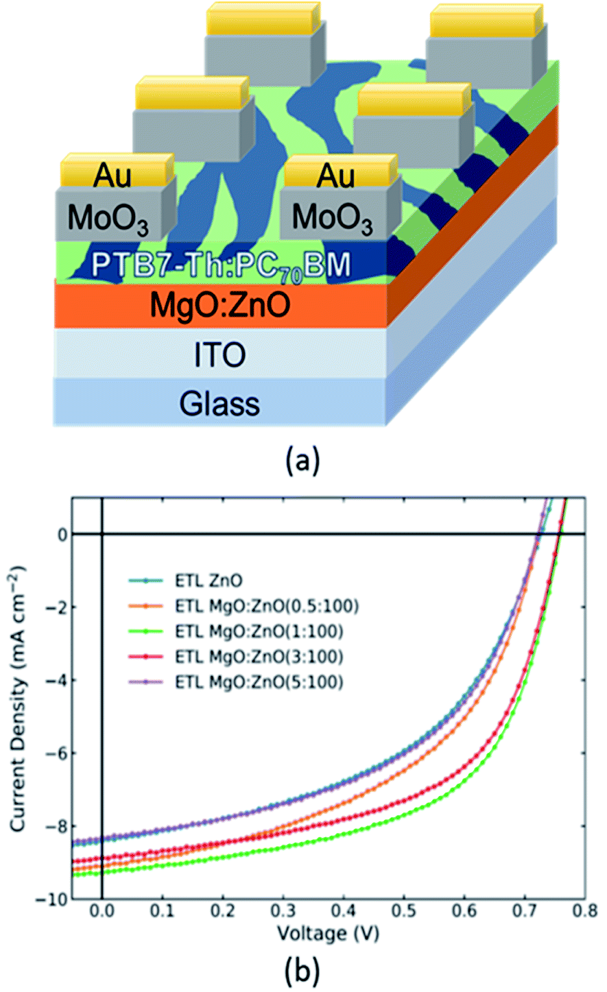 | ||
| Fig. 1 (a) Schematic of the multi-layered structure of the OPV device. 5 Types of OPVs were tested, 4 with ETLs containing different amounts of Mg-doping in ZnO and an undoped “control” device. (b) Representative current density vs. voltage curves under 1 sun. Corresponding average key performance indicators from 8 distinct devices for each type of ETL are reported in Table 2. | ||
Photovoltaic performance of Mg-doped ZnO based organic photovoltaics
The current density–voltage characteristics at 1 sun for PTB7-Th:PC70BM OPVs employing the undoped ZnO ETL vs. the Mg-doped ZnO ETLs with varying Mg content are shown in Fig. 1b. The corresponding average key PV performance indicators are displayed in Table 2. The results confirm that an enhancement in the efficiency of OPVs can be achieved by doping the ZnO ETL with Mg, via the direct addition of the MgO precursor to the ZnO precursor solution to form a single composite ETL using an annealing temperature of 150 °C. The best performing device employing the Mg-doped ZnO ETL was formed from a MgO:ZnO precursor ratio of 1:100 and has a relative increase in PCE of ≈18% with respect to the control device employing the undoped ZnO ETL. This is a consequence of an increase in the JSC, VOC and FF. The device with the ETL formed from a MgO:ZnO precursor ratio of 5:100, is exhibiting lower PCE than the undoped ZnO control. As the Mg content increases in the doped ZnO ETLs, the JSC and FF of the devices increase, reaching a peak value in the region of 1–3% Mg doping level. The values of JSC and FF then decrease with additional Mg doping. For the VOC there are slight variations between the devices, but similarly, the highest VOC is achieved at 1–3% doping. These results are consistent with findings for Mg-doped ZnO ETLs formed with an annealing temperature of 150 °C that were applied to perovskite PVs.56 The results reported herein demonstrate that this strategy can be viable in the case of OPVs as well. Further testing in a sub-divided region of 1–3% Mg doping can be used to obtain an “optimised” doping level. The applicability of the Mg-doped ZnO ETLs has also been tested and shown to be successful for the case where the non-fullerene acceptor PM6:Y6 system has been used as the active layer in OPV devices (see Fig. S2, Tables S3 and S4‡). Similarly, the optimum Mg-doping is found to be in the region of ≈1–3%.
| ETL (MgO:ZnO) |
PCE (%) | J SC (mA cm−2) | V OC (mV) | FF |
|---|---|---|---|---|
| ZnO | 3.21 ± 0.07 | 8.46 ± 0.04 | 736 ± 1 | 0.52 ± 0.01 |
| (0.5:100) |
3.32 ± 0.07 | 8.99 ± 0.04 | 721 ± 1 | 0.51 ± 0.01 |
| (1:100) |
3.79 ± 0.07 | 9.05 ± 0.04 | 742 ± 1 | 0.56 ± 0.01 |
| (3:100) |
3.71 ± 0.07 | 8.80 ± 0.04 | 739 ± 1 | 0.57 ± 0.01 |
| (5:100) |
3.08 ± 0.07 | 8.44 ± 0.04 | 734 ± 1 | 0.50 ± 0.01 |
To identify the possible reasons behind the observed trends, thin films of the undoped ZnO ETL as well as films of the Mg-doped ZnO ETLs formed from MgO:ZnO precursor ratios of 1:100 and 5:100 (that exhibited the biggest variations in OPV performance) have undergone further physical and optical characterisation. In addition, the corresponding OPV devices have been subject to further electrical testing.
It is important to note that the optimum doping level range for the ETL is dependent on the annealing temperature employed. To demonstrate this, we have also tested OPVs containing ETLs formed with an annealing temperature of 300 °C (see Fig. S3 and Table S5‡). The OPV devices employing the undoped ZnO ETL and the ETL formed from a MgO:ZnO precursor ratio of 1:100 show better performance when the ETL is annealed at 150 °C rather than 300 °C. At 300 °C the optimum Mg-doping is no longer in the range 1–3%.
As OPV devices approach commercial application, an increasingly important property to test for is stability. To test for stability, devices were measured on the day of fabrication and then kept under identical conditions before re-measurement after 45 days. The percentage decrease in PCE when re-measuring devices was 16.2% for the device containing the undoped ZnO ETL vs. 13.3% and 8.1% for the devices with ETLs formed from MgO:ZnO precursor ratios of 1:100 and 5:100 respectively. Therefore the presence of Mg is favourable in terms of device stability as well.
Characterisation of Mg-doped ZnO electrodes
| ETL (MgO:ZnO) |
Φ (eV) (Kelvin Probe) | Φ (eV) (UPS) | VB onset (eV) |
|---|---|---|---|
| ZnO | 4.2 ± 0.1 | 3.6 ± 0.1 | 3.6 ± 0.1 |
| (1:100) |
4.1 ± 0.1 | 3.6 ± 0.1 | 3.6 ± 0.1 |
| (5:100) |
4.1 ± 0.1 | 3.7 ± 0.1 | 3.6 ± 0.1 |
:PC70BM blend on top of the undoped and Mg-doped ZnO ETLs, via tapping mode AFM and we report the corresponding images in Figure 2(a–c). There are only insignificant variations in Sq between the films (smaller than the uncertainties), hence, it can be inferred that for the length scales investigated here, Mg-doping of the ETL does not influence the morphology of the blend. We report the AFM images of the corresponding ETL films without the blend on top in Fig. 2d–f respectively for the different Mg loadings. The variation in Sq between the ETL formed from a MgO:ZnO precursor ratio of 1:100 and the undoped ZnO ETL is smaller than the uncertainties in the measurements, however, there is a ≈ 20% increase in Sq for the ETL formed from a MgO:ZnO precursor ratio of 5:100. Such an increase in Sq is indicative of a less uniform and less homogeneous surface of the ETL at ≈5% loading, with potential phase separation and formation of MgO-rich regions which may influence negatively the OPV performance (vide infra).
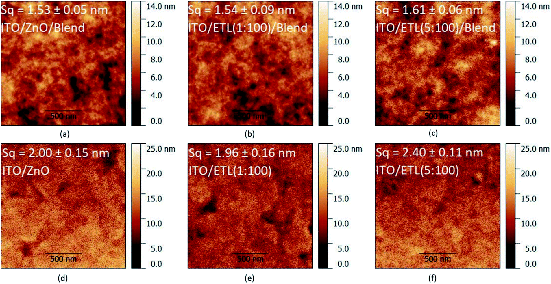 | ||
| Fig. 2 Tapping mode AFM images (1.6 μm × 1.6 μm, annotated with the corresponding root mean square roughness (Sq)) of the topography of (a) ITO/ZnO/PTB7-Th:PC70BM, (b) ITO/Mg-doped (1:100) ZnO/PTB7-Th:PC70BM, (c) ITO/Mg-doped (5:100) ZnO/PTB7-Th:PC70BM, (d) ITO/ZnO, (e) ITO/Mg-doped (1:100) ZnO and (f) ITO/Mg-doped (5:100) ZnO. There is no significant variation of Sq between the bare ITO/ZnO and ITO/Mg-doped (1:100) ZnO films, although Sq is ≈20% larger for the (5:100) MgO:ZnO films. Mg-doping of the ETL does not influence the morphology of the PTB7-Th:PC70BM blend for the investigated length scales. | ||
:ZnO precursor ratio of 1:100 exhibits a lower Hall mobility than the undoped ZnO film. The film formed from the MgO:ZnO precursor ratio of 5:100, even though expected to show an even lower Hall mobility, exhibits a Hall mobility that it is very similar to the undoped ZnO thin film. This might be the result of a potential phase separation between ZnO and MgO that appears to occur for this higher level of Mg doping, as suggested by the rougher morphology of these films observed in the AFM investigation. The resistivity of a film is proportional to the inverse of the product of carrier concentration and mobility. This leads to the highest resistivity obtained when the ETL is formed from the MgO:ZnO precursor ratio of 1:100.
| ETL (MgO:ZnO) |
Hall mobility (cm2 V−1 s−1) | Carrier concentration (×1021 cm−3) | Resistivity (×10−5 Ω cm) |
|---|---|---|---|
| ZnO | 39.8 ± 0.05 | 1.86 ± 0.03 | 8.44 ± 0.01 |
| (1:100) |
34.8 ± 0.05 | 2.00 ± 0.11 | 8.97 ± 0.01 |
| (5:100) |
40.9 ± 0.05 | 2.03 ± 0.06 | 7.51 ± 0.01 |
:PC70BM or PM6:Y6 blend layer on top of the undoped and Mg-doped ZnO ETLs (see Fig. S6‡). The samples incorporating the Mg-doped ZnO show a slightly increased transmittance (≈8% in relative terms) throughout the tested spectral region (300–900 nm). The increase in JSC observed in the OPV devices is thus not associated with increased absorption in the active layer blend.
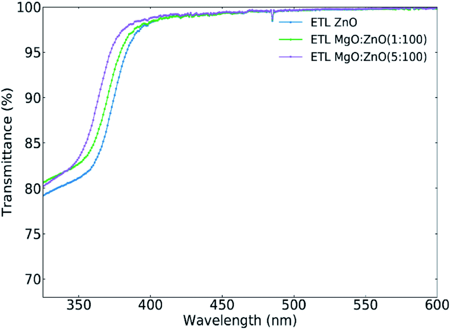 | ||
| Fig. 3 Transmission spectra of thin films of ZnO and Mg-doped ZnO. There is a blue-shift in the spectrum with increasing Mg-doping. | ||
:PC70BM based OPV devices. For the corresponding figure of the PM6:Y6 based OPV devices see Fig. S7.‡ The incremental addition of Mg in the ZnO ETL leads to a corresponding reduction in the current leakage in the OPV device. This is evidenced in Fig. 4a (Fig. S7a‡), where the (dark) current vs. voltage characteristics of the OPV diodes are shown. This reduced leakage is indicative of an increased shunt resistance (see Fig. S8‡). The average current density at −1 V is −1.41 × 10⁻³ mA cm−2 for the undoped ZnO ETL and decreases to −3.31 × 10⁻⁴ mA cm−2 for the Mg-doped ZnO ETL device formed from a MgO:ZnO precursor ratio of 1:100 and further decreases to −1.18 × 10⁻⁴ mA cm−2 for the Mg-doped ZnO ETL device formed from a MgO:ZnO precursor ratio of 5:100. A corresponding increase in Rsh is observed, with Rsh calculated as 4.35 × 10⁶ Ω cm2, 1.17 × 10⁷ Ω cm2 and 1.42 × 10⁷ Ω cm2 respectively. A similar trend is observed in the corresponding average current density at −1 V and resulting Rsh values for the PM6:Y6 devices as well (see Table S6‡). To gain further insight in the extraction properties and the recombination in these devices, we have investigated the dependence of the photocurrent density (JPH) on the effective voltage (VEFF)62 and measured the decay and rise times of the VOC. The JPH and VEFF can be calculated using the expressions JPH = |JL − JD| and VEFF = V0 − Va where JL and JD are the measured photocurrents under illumination and in the dark respectively, Va is the externally applied voltage and V0 is the (externally applied) voltage at JPH = 0. Fig. 4b (Fig. S7b‡) shows the variation of the JPH with VEFF. As expected from the PV characterisation, the Mg-doped ZnO ETL device formed from a MgO:ZnO precursor ratio of 1:100 shows the best performance. The extraction of JPH at saturation (JPH,SAT) which occurs at high VEFF (∼1.1 V where the device in reverse bias) as well its extraction at short circuit (JPH,SC) allow for the calculation of an indicator that can be used to quantify the variation in performance of the devices with differing Mg doping. Such an indicator is the ratio JPH,SC/JPH,SAT (PDISS) which some authors consider akin to the relative exciton dissociation efficiency.31,32,36 We note in this regard that since such a parameter is calculated as a ratio of collected currents it will not account for any recombination event taking place even at the strongest fields applied “in saturation” (as specified above). It does however provide information on the effectiveness with which dissociated excitons are extracted. We find PDISS increases from 95.85% for the undoped ZnO device to 96.76% for the 1:100 Mg-doped ZnO device before decreasing to 95.83% at 5:100 Mg loading. Similarly, for the case of PM6:Y6 devices, PDISS increases from 94.88% for the undoped ZnO device to 95.72% for the 1:100 Mg-doped ZnO device before decreasing to 94.37% at 5:100 Mg loading. Finally, Fig. 4c and d (Fig. S7c and S7d‡), demonstrate the time dependent VOC decay and rise for the OPV devices. The OPV device based on the Mg-doped ZnO ETL formed from a MgO:ZnO precursor ratio of 1:100 takes the longest time to be completely discharged in comparison to the other devices. This also holds for the PM6:Y6 based OPVs. In addition, it requires a shorter rise time to arrive at the maximum VOC (for PM6:Y6 rise times are similar between the undoped ZnO device and the 1:100 Mg-doped ZnO device and slower for the 5:100 doped ZnO device). The trends observed in the open circuit voltage and decay studies are indicative of reduced recombination in the 1:100 Mg-doped ZnO device.63,64
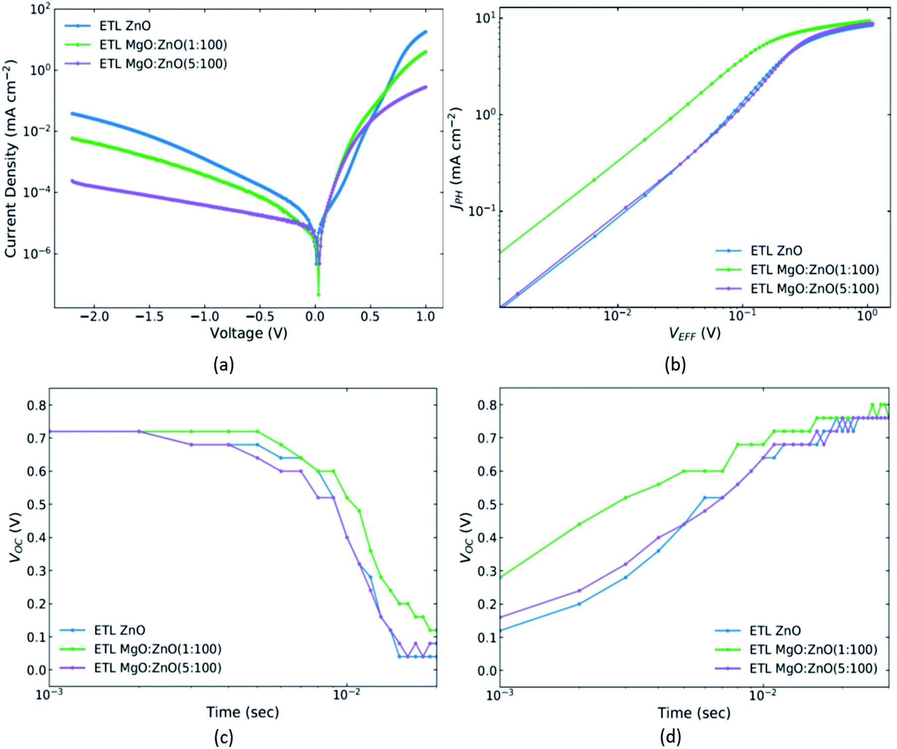 | ||
| Fig. 4 (a) Current density–voltage curves in the dark. (b) Photocurrent density–effective voltage curves. (c) Open circuit voltage decay curves (in the dark). (d) Open circuit voltage rise curves (under 1 sun). | ||
Discussion
The results above show that low-temperature annealing of a mixed MgO:ZnO precursor leads to a significant increase of the performance parameters of OPVs incorporating such an ETL, and in particular an ≈18% relative increase of the PCE with respect to undoped ZnO ETLs for films with a ≈ 1% atomic Mg doping.
Interestingly, analysis of the electrical properties of the OPVs reveal a higher shunt resistance (accounting for the reduced losses for such devices, also evidenced by the faster increase of the VOC upon light switch-on and the slower VOC decay after light switch-off, as well as by the decreased dark current in reverse bias (Fig. 4a)). The increased JPH on the other hand (Fig. 4b) indicates a reduction in the series resistance (Rs) which would also lead to an increase of both the JSC and of the FF, as indeed observed. Of course, the increased Rsh also accounts for the increased VOC, and JSC.
To gather some insight into the microscopic origin of such loss reductions we note that the properties of ZnO films are well-established to be highly dependent on the presence and/or concentration of defects such as oxygen vacancies, zinc interstitials and/or other dopants.65 For example, it has been proposed that Mg can reduce the density of oxygen vacancies in ZnO nanorods.66 In our case as well, we suggest that Mg doping compensates oxygen vacancies which may act as charge recombination centres. In addition, we note that bulk MgO is characterised by a rather large ionisation potential (∼10 eV) compared to ZnO (∼7.6 eV), thereby suggesting significantly better hole-blocking properties for any MgO-rich region of the modified electrodes, which would also contribute to reduction of PV losses linked to hole currents flowing through the electron-collecting electrode.
The question arises as to how much Mg will provide optimum results. Our data show that the best results are obtained with a Mg loading between ≈1 and 3%, but that when increasing this to ≈5%, despite a higher Rsh (expected for the more insulating nature of MgO) carrier recombination becomes significant (e.g. from Fig. 4c and d) eventually leading to a lower PCE. It is interesting that the Hall (lateral) resistivity at ≈5% Mg is decreased with respect to undoped and ≈1%-doped ETLS, with a concomitant increase of the electron mobility, thereby hinting at a potential overcompensation of the oxygen vacancies, with a concomitant increase of carrier recombination centres. This is also corroborated by the morphology changes visible in AFM images at such a concentration (Fig. 2).
In summary we propose that ≈1% Mg doping strikes the “right balance” between the various processes at play, i.e., extraction of the electrons, blocking of the holes and hole–electron recombination.
Conclusions
We have shown that Mg acetate can be directly added to ZnO precursor solutions to form Mg-doped ZnO ETLs for OPVs with a reduced annealing temperature of 150 °C. Not only is this appealing for low-temperature industrial manufacturing and greater sustainability, but also affords greater OPV PCEs. We obtained our best results with a 1:100 MgO:ZnO precursor concentrations and this yields a relative increase in efficiency of ≈18% compared to devices incorporating undoped ZnO ETLs. This exceeds the relative improvement in efficiency we have previously reported (≈10%) when MgO was used on top of ZnO (i.e. effectively forming a bilayer). The increase in PCE observed in this work, is a result of an enhanced JSC, VOC and FF, which we can trace down to an improved contact with the active layer exhibiting a decreased recombination and leakage current. Doping with low levels of Mg does not significantly affect the work function or blend morphology. Our results show that for achieving better performance the Mg doping needs to be limited when the annealing temperature used is 150 °C, as doping in the ETL formed from a MgO:ZnO precursor ratio of 5:100 is already excessive and can hinder performance. The Mg-doped devices show enhanced stability and this strategy is viable for OPVs based both on fullerene and non-fullerene acceptor active layer blends. Our work provides an industrially scalable approach to electrodes for high-performance OPVs and is in principle applicable to both top and bottom contact electrodes.
Conflicts of interest
“There are no conflicts to declare”.Acknowledgements
Special thanks to Natalie Stingelin and Marcello Righetto for useful discussions. We acknowledge use of the London Centre for Nanotechnology Atomic Force Microscope Facility. I. I. was supported by the EPSRC and SFI Centre for Doctoral Training in Advanced Characterisation of Materials (Grant Ref: EP/L015277/1). G. L. and E. L.-K. thank Professor N. Koch (HU Berlin) for granting access to photoemission tools, DFG (Project No. 182087777-SFB 951) and the HySPRINT Innovation Lab at Helmholtz-Zentrum Berlin (through the framework of the Joint Lab GEN_FAB) for financial support. K. G. acknowledges funding from the Royal Society through a Newton International Fellowship. F. C. thanks EPSRC for financial support via grant EP/P007767/1.Notes and references
- G. M. Lazzerini, F. Di Stasio, C. Flechon, D. J. Caruana and F. Cacialli, Appl. Phys. Lett., 2011, 99, 243305 CrossRef.
- N. S. Lewis and D. G. Nocera, Proc. Natl. Acad. Sci. U. S. A., 2007, 103, 15729–15735 CrossRef PubMed.
- C. J. Brabec, A. Distler, X. Y. Du, H. J. Egelhaaf, J. Hauch, T. Heumueller and N. Li, Adv. Energy Mater., 2020, 10, 2001864 CrossRef CAS.
- J. Barsotti, A. G. Rapidis, I. Hirata, F. Greco, F. Cacialli and V. Mattoli, Adv. Electron. Mater., 2021, 7, 2001145 CrossRef CAS.
- I. Ierides, A. Zampetti and F. Cacialli, Curr. Opin. Green Sustainable Chem., 2019, 17, 15–20 CrossRef.
- L. Kinner, T. Dimopoulos, G. Ligorio, E. J. W. List-Kratochvil and F. Hermerschmidt, RSC Adv., 2021, 11, 17324–17331 RSC.
- P. W. M. Blom, Adv. Mater. Technol., 2020, 5, 2000144 CrossRef CAS.
- R. Sorrentino, E. Kozma, S. Luzzati and R. Po, Energy Environ. Sci., 2021, 14, 180–223 RSC.
- Z. Yin, J. Wei and Q. Zheng, Adv. Sci., 2016, 3, 1500362 CrossRef PubMed.
- M. Graetzel, R. A. J. Janssen, D. B. Mitzi and E. H. Sargent, Nature, 2012, 488, 304–312 CrossRef CAS PubMed.
- K. Mahmood, S. Sarwar and M. T. Mehran, RSC Adv., 2017, 7, 17044–17062 RSC.
- H. L. Yip and A. K. Y. Jen, Energy Environ. Sci., 2012, 5, 5994–6011 RSC.
- C. Y. Chan, Y. F. Wei, H. T. Chandran, C. S. Lee, M. F. Luo and T. W. Ng, RSC Adv., 2015, 5, 77071–77074 RSC.
- J. C. D. Faria, A. J. Campbell and M. A. McLachlan, Adv. Funct. Mater., 2015, 25, 4657–4663 CrossRef CAS.
- Z. Liang, Q. Zhang, L. Jiang and G. Cao, Energy Environ. Sci., 2015, 8, 3442–3476 RSC.
- J. C. Wang, W. T. Weng, M. Y. Tsai, M. K. Lee, S. F. Horng, T. P. Perng, C. C. Kei, C. C. Yu and H. F. Meng, J. Mater. Chem., 2010, 20, 862–866 RSC.
- J. B. Franklin, B. Zou, P. Petrov, D. W. McComb, M. P. Ryan and M. A. McLachlan, J. Mater. Chem., 2011, 21, 8178–8182 RSC.
- A. Rivera, A. Mazady, K. Ahi and M. Anwar, Proc. SPIE, 2015, 9483, 948301–948307 CrossRef.
- S. Schumann, R. Da Campo, B. Illy, A. C. Cruickshank, M. A. McLachlan, M. P. Ryan, D. J. Riley, D. W. McComb and T. S. Jones, J. Mater. Chem., 2011, 21, 2381–2386 RSC.
- Y. Lin, Y. Firdaus, M. I. Nugraha, F. Liu, S. Karuthedath, A. H. Emwas, W. Zhang, A. Seitkhan, M. Neophytou, H. Faber, E. Yengel, I. McCulloch, L. Tsetseris, F. Laquai and T. D. Anthopoulos, Adv. Sci., 2020, 7, 1903419 CrossRef CAS PubMed.
- X. Du, Y. Yuan, L. Zhou, H. Lin, C. Zheng, J. Luo, Z. Chen, S. Tao and L. S. Liao, Adv. Funct. Mater., 2020, 30, 1909837 CrossRef CAS.
- Y. Sun, J. H. Seo, C. J. Takacs, J. Seifter and A. J. Heeger, Adv. Mater., 2011, 23, 1679–1683 CrossRef CAS PubMed.
- J. Zhang, H. Yang, X. Zhang, M. Morbidoni, C. H. Burgess, R. Kilmurray, S. Feng and M. A. McLachlan, Inorg. Chem. Front., 2020, 7, 2809–2817 RSC.
- J. Zhang, M. Morbidoni, C. H. Burgess, J. Wu, T. Du, K. Harrabi, D. J. Payne, J. R. Durrant and M. A. McLachlan, Cryst. Growth Des., 2017, 17, 6559–6564 CrossRef CAS.
- J. Zhang, J. C. D. Faria, M. Morbidoni, Y. Porte, C. H. Burgess, K. Harrabi and M. A. McLachlan, Adv. Electron. Mater., 2016, 2, 1600008 CrossRef.
- X. Zhang, Y. Sun, M. Wang, H. Cui, W. Xie, L. Shen and W. Guo, Sol. Energy, 2019, 181, 9–16 CrossRef CAS.
- T. M. Brown, G. M. Lazzerini, L. J. Parrott, V. Bodrozic, L. Burgi and F. Cacialli, Org. Electron., 2011, 12, 623–633 CrossRef CAS.
- I. Ierides, I. Squires, G. Lucarelli, T. M. Brown and F. Cacialli, J. Mater. Chem. C, 2021, 9, 3901–3910 RSC.
- M. Li, J. Li, L. Yu, Y. Zhang, Y. Dai, R. Chen and W. Huang, Front. Chem., 2020, 8, 399 CrossRef CAS PubMed.
- Y. Xia, C. Wang, B. Dong, G. Wang, Y. Chen, R. C. I. MacKenzie, W. Dong, S. Ruan, Y. Liu and S. Wen, ACS Appl. Mater. Interfaces, 2021, 13, 14423–14432 CrossRef CAS PubMed.
- B. Guo, J. Han, J. Qiu, C. Yu, Y. Sun, F. Li, Z. Hu and Y. Wang, ACS Appl. Mater. Interfaces, 2017, 9, 42969–42977 CrossRef CAS PubMed.
- C. Hou and H. Yu, Chem. Eng. J., 2021, 407, 127192 CrossRef CAS.
- S. Park, R. Kang and S. Cho, Curr. Appl. Phys., 2020, 20, 172–177 CrossRef.
- B. Usmani, R. Ranjan, Prateek, S. K. Gupta, R. K. Gupta, K. S. Nalwa and A. Garg, Sol. Energy, 2021, 214, 220–230 CrossRef CAS.
- D. Chi, S. Lu, R. Xu, K. Liu, D. Cao, L. Wen, Y. Mi, Z. Wang, Y. Lei, S. Qu and Z. Wang, Nanoscale, 2015, 7, 15251–15257 RSC.
- X. Song, G. Liu, P. Sun, Y. Liu and W. Zhu, J. Phys. Chem., 2021, 12, 10616–10621 CAS.
- M. Wang, Y. Sun, J. Guo, Z. Li, C. Liu and W. Guo, Org. Electron., 2019, 74, 258–264 CrossRef CAS.
- M. Chrzanowski, M. Kuchowicz, R. Szukiewicz, P. Sitarek, J. Misiewicz and A. Podhorodecki, Org. Electron., 2020, 80, 105656 CrossRef CAS.
- H. M. Kim, S. Cho, J. Kim, H. Shin and J. Jang, ACS Appl. Mater. Interfaces, 2018, 10, 24028–24036 CrossRef CAS PubMed.
- Y. Sun, Y. Jiang, H. Peng, J. Wei, S. Zhang and S. Chen, Nanoscale, 2017, 9, 8962–8969 RSC.
- L. Wang, J. Lin, X. Liu, S. Cao, Y. Wang, J. Zhao and B. Zou, J. Phys. Chem. C, 2020, 124, 8758–8765 CrossRef CAS.
- H. M. Kim, W. Jeong, J. H. Kim and J. Jang, Nanomaterials, 2020, 10, 2423 CrossRef CAS PubMed.
- L. Wang, J. Pan, J. Qian, W. Lei, Y. Wu, W. Zhang, D. K. Goto and J. Chen, J. Mater. Chem. C, 2018, 6, 8099–8104 RSC.
- M. M. Yan, Y. Li, Y. T. Zhou, L. Liu, Y. Zhang, B. G. You and Y. Li, IEEE Photonics J., 2017, 9, 8200508 Search PubMed.
- S. B. Heo, J. S. Shin, T. Y. Kim, S. Park, W. H. Jung, H. Kim, J. A. Hong, B. S. Kim, Y. Park, B. D. Chin, J. G. Kim and S. J. Kang, Curr. Appl. Phys., 2021, 29, 107–113 CrossRef.
- H. Wu, Y. Zhang, X. Zhang, M. Lu, C. Sun, T. Zhang and W. W. Yu, Adv. Opt. Mater., 2017, 5, 1700377 CrossRef.
- Y. J. Lin, P. H. Wu, C. L. Tsai, C. J. Liu, Z. R. Lin, H. C. Chang and C. T. Lee, J. Appl. Phys., 2008, 103, 113709 CrossRef.
- G. El Hallani, S. Nasih, N. Fazouan, A. Liba, M. Khuili, M. Sajieddine, M. Mabrouki, L. Laanab and E. H. Atmani, J. Appl. Phys., 2017, 121, 135103 CrossRef.
- A. Singh and P. Kumar, J. Optoelectron. Adv. Mater., 2014, 16, 311–316 Search PubMed.
- L. Meng, X. Yang, H. Chai, Z. Lv and T. Yang, Thin Solid Films, 2019, 672, 186–191 CrossRef CAS.
- A. Ringleb, R. Ruess, N. Hofeditz, W. Heimbrodt, T. Yoshida and D. Schlettwein, Phys. Chem. Chem. Phys., 2021, 23, 8393–8402 RSC.
- C. J. Raj, K. Prabakar, S. N. Karthick, K. V. Hemalatha, M. K. Son and H. J. Kim, J. Phys. Chem. C, 2013, 117, 2600–2607 CrossRef CAS.
- I. Biswas, P. Roy, U. Maity, P. K. Sinha and A. K. Chakraborty, Thin Solid Films, 2020, 711, 138301 CrossRef CAS.
- M. Xing, Y. Wei, D. Wang, Q. Shen and R. Wang, Curr. Appl. Phys., 2021, 21, 14–19 CrossRef.
- J. Song, E. Zheng, L. Liu, X. F. Wang, G. Chen, W. Tian and T. Miyasaka, Chemsuschem, 2016, 9, 2640–2647 CrossRef CAS PubMed.
- X. Li, J. Yang, Q. Jiang, W. Chu, J. Xin, J. Hou and H. Lai, Electrochim. Acta, 2018, 261, 474–481 CrossRef CAS.
- R. T. Ginting, C. C. Yap, M. Yahaya and M. M. Salleh, J. Alloys Compd., 2014, 585, 696–702 CrossRef CAS.
- Z. Yin, Q. Zheng, S. C. Chen, D. Cai, L. Zhou and J. Zhang, Adv. Energy Mater., 2014, 4, 1301404 CrossRef.
- B. A. MacLeod, P. Schulz, S. R. Cowan, A. Garcia, D. S. Ginley, A. Kahn and D. C. Olson, Adv. Energy Mater., 2014, 4, 1400073 CrossRef.
- N. Johansson, F. Cacialli, K. Z. Xing, G. Beamson, D. T. Clark, R. H. Friend and W. R. Salaneck, Synth. Met., 1998, 92, 207–211 CrossRef CAS.
- J. S. Kim, B. Lagel, E. Moons, N. Johansson, I. D. Baikie, W. R. Salaneck, R. H. Friend and F. Cacialli, Synth. Met., 2000, 111–112, 311–314 CrossRef CAS.
- V. D. Mihailetchi, H. Xie, B. de Boer, L. J. A. Koster and P. W. M. Blom, Adv. Funct. Mater., 2006, 16, 699–708 CrossRef CAS.
- J. Dagar, S. Castro-Hermosa, G. Lucarelli, F. Cacialli and T. M. Brown, Nano Energy, 2018, 49, 290–299 CrossRef CAS.
- J. Vollbrecht and V. V. Brus, Energies, 2021, 14, 4800 CrossRef CAS.
- A. Janotti and C. G. Van de Walle, Rep. Prog. Phys., 2009, 72, 126501 CrossRef.
- X. Yu, X. Yu, M. Yan, T. Weng, L. Chen, Y. Zhou and J. Wei, Sens. Actuators, A, 2020, 312, 112163 CrossRef CAS.
Footnotes |
| † Dedicated in memory of Alasdair J. Campbell. |
| ‡ Electronic supplementary information (ESI) available. See https://doi.org/10.1039/d1se02001c |
| This journal is © The Royal Society of Chemistry 2022 |