
Nano-engineering and nano-manufacturing in 2D materials: marvels of nanotechnology
Sharidya
Rahman
 *a and
Yuerui
Lu
*ab
*a and
Yuerui
Lu
*ab
aSchool of Engineering, College of Engineering and Computer Science, The Australian National University, Canberra, ACT 2601, Australia. E-mail: sharidya.rahman@anu.edu.au
bARC Centre for Quantum Computation and Communication Technology, Department of Quantum Science, School of Engineering, The Australian National University, Acton, ACT 2601, Australia. E-mail: yuerui.lu@anu.edu.au
First published on 27th June 2022
Abstract
Two-dimensional materials have attracted significant interest and investigation since the marvellous discovery of graphene. Due to their unique physical, mechanical and optical properties, van der Waals (vdW) materials possess extraordinary potential for application in future optoelectronics devices. Nano-engineering and nano-manufacturing in the atomically thin regime has further opened multifarious avenues to explore novel physical properties. Among them, moiré heterostructures, strain engineering and substrate manipulation have created numerous exotic and topological phenomena such as unconventional superconductivity, orbital magnetism, flexible nanoelectronics and highly efficient photovoltaics. This review comprehensively summarizes the three most influential techniques of nano-engineering in 2D materials. The latest development in the marvels of moiré structures in vdW materials is discussed; in addition, topological structures in layered materials and substrate engineering on the nanoscale are thoroughly scrutinized to highlight their significance in micro- and nano-devices. Finally, we conclude with remarks on challenges and possible future directions in the rapidly expanding field of nanotechnology and nanomaterial.
 Sharidya Rahman | Sharidya Rahman received his BEng Degree from the Faculty of Engineering, University of Malaya, Malaysia in 2017. Currently, he is a Research Scholar and Doctoral Candidate at the School of Engineering, Australian National University (ANU), Australia under the supervision of Professor Yuerui Lu in the NEMS Laboratory. His research interests focus on novel and emerging nanomaterials, magnetic properties of vdW multiferroics and low-dimensional materials, heterostructures and super lattices of layered nanomaterials, nano-manufacturing technologies, and 2D nanotechnology for future non-linear optics, photonics, spintronic, quantum science, optoelectronics, and solar cells. |
 Yuerui Lu | Yuerui Lu is a Professor at the Australian National University (ANU). He received his PhD Degree from Cornell University, School of Electrical and Computer Engineering. He holds a BS Degree in Applied Physics from the University of Science and Technology of China. Currently, he is leading the Nano-Electro-Mechanical System (NEMS) Lab at the ANU. His research interests include MEMS/NEMS sensors and actuators, nanomanufacturing technologies, renewable energy harvesting, biomedical novel devices, and 2D materials and devices. |
Introduction
The family of 2D materials has expanded, encompassing a wide variety of layered compounds with new additions occurring sporadically. Graphene and transition metal dichalcogenides (TMDCs) have been investigated extensively in the past decade,1–6 shedding light on several applications and fundamental physics.7–11 Recently, nano-engineering and nano manufacturing in the form of moiré heterostructures,12 wrinkle and fold formation13 and substrate modulation14 have led to numerous emergent and intriguing properties including superconductivity,15 correlated insulator states,16 topological conducting channels,17,18 ferromagnetism,19 enhanced electron mobility,20 harmonic generation and remarkable optoelectronic properties.18,21,22 This advancement in nanotechnology at the atomic level has been leveraged in a wide range of applications such as mechanically reconfigurable quantum materials, wearable electronics and nanosystems.23–26A moiré superlattice emerges when two similar materials are super positioned with different angles relative to each other, resulting in different periodicity-like moiré patterns.27 In the case of homogenous materials, the relative twist mainly affects the moiré superlattice, while in heterostructures, both the stacking angle and lattice mismatch have a noticeable effect. Therefore, altering the twist angle has been demonstrated as a powerful tool in the nano regime to modulate the lattice structure, topological properties and band structure of materials.28–32 In addition, the translation shift33,34 and stacking angle greatly stimulate the interlayer interaction and alter the phonon bands and charge distribution, resulting in a significant variation in the Raman signature of materials.27 This further provides an excellent platform for exploring interlayer coupling and Moire phonons.
Strain engineering is considered a vital technique for modulating the lattice and electronic structure of 2D materials, and thus tune their optoelectronic properties. Wrinkle and fold formation in atomically thin materials is the most straightforward way of nano-manufacturing.35,36 Compared to their 3D and bulk counterparts, thin 2D materials show greater potential for strain engineering due to their stronger deformation capacity and ability to withstand elevated elastic strain. For instance, monolayer graphene can withstand up to 25% elastic strain.37 Furthermore, small changes in the lattice strain can significantly modulate physical properties such as phonon structure and energy band, which results in a change in the Raman and photoluminescence (PL) peaks of 2D materials.38,39 In addition, strain can also manipulate the magnetism in layered ferromagnetic compounds and induce magnetism in non-magnetic materials.40,41 Therefore, self-assembled nanostructures are highly beneficial for the fabrication of stretchable optoelectronics owing to their unique morphology and ability to resist deformation.
The dielectric environment is also a critical modulating factor to entirely understand the properties of 2D materials and distinguish their intrinsic properties from extrinsic properties, which are largely dependent on the substrate interactions. Commonly, a high k dielectric is employed to mitigate Coulomb scattering, enhance the mobility of electrons and on/off ratio, either through encapsulation or through substrate choice.42,43 Furthermore, it can also stimulate the production of many body scattering in atomically thin materials.44 Freestanding materials over holes and patterned trenches also undergo strain, which can affect their physical and optoelectronics properties.45 Hence, substrate engineering is crucial in comprehending and manipulating the optical dynamics of layered materials.
In this review, we provide a comprehensive summary of the three major nano-engineering techniques employed in 2D materials, which have attracted proliferated interest and broadened their application sector. Existing reviews and the literature fail to address the significance and importance of these nano-engineering techniques in 2D materials, which have not been comprehensively reviewed to date. Although the literatures addresses multiple structural engineering and quantum confinement technologies in 2D materials,46,47 an in-depth review on moiré phonons, topological structures and thermal transport through suspended structures has not been presented in a single work. Firstly, we briefly present the methods to fabricate moiré superlattices, and then deeply investigate the moiré phonons and crystallographic related phonons in twisted layered materials, which are characterized mostly through Raman spectroscopy.48 Next we highlight wrinkle and folded nanostructures in 2D materials, focusing on their formation methods and mechanisms, structural features and non-linear optical properties. Finally, we provide an insight into suspended materials using trenched substrates, which has prevailed as another common form of nano-engineering. We outline the importance of the dielectric environment on basic linear and nonlinear optical properties, in addition to thermal transport and conductivity properties. In the concluding remarks, we outline some technological challenges and possible future studies in this exciting direction of nanotechnology.
Marvels of moiré
Formation and fabrication of moiré superlattice
The surfaces of 2D materials lack dangling bonds, unlike traditional semiconductors, and in layered systems, van der Waals interaction bind monolayers together. Therefore, the so-called vdW heterostructures are generated when two or more specific 2D materials with distinct symmetry or cell length are stacked vertically. In a vdW system, monolayers can be stacked with a certain or random orientation, resulting in a sophisticated structure with certain interlayer twist angle. Furthermore, it is possible for individual monolayers to possess different crystal structures and cell lengths, and during heterostructure formation, they can generate long-range quasi-periodic patterns. The resulting structures are known as moiré patterns and moiré superlattices (MSL) refer to the quasi-periodic cells.49–51 The MSL of heterostructures and few-layered materials can drastically impact their intralayer properties, which alter the properties of the entire system. Reciprocal lattices of MSL can modulate the momentum space and interlayer separation, which can alter the phonon modes and charge distribution. This leads to a prominent transition in spin states, band structures and topological phases.27 Moiré patterns can also be formed in homostructures, where a relative twist exists between the same constituents. For instance, bilayer graphene is known to exhibit a twisted homostructure,12 where a moiré pattern can profoundly alter its physical properties. The moiré pattern can further affect the mini Brillion zone, where the weak quasi-periodic potential of the MSL with a long wavelength can trigger the formation of minibands.52–54 In bilayer graphene, it leads to the formation of secondary Dirac cones,55–57 and in special cases, arising at specific interlayer twist angles, the first and second moiré band can flatten completely when filled partially and form strongly correlated states.58,59 For instance, a twist angle of ∼1.1°, also known as the magic angle, in bilayer graphene can lead to astounding physical properties such as superconductivity at 4 K and Mott states.15,60 Hence, the advantages of moiré structures are immense and in many cases outweigh the functional benefits of monolayer 2D materials, where these distinct properties cannot be detected. Thus, it is important to create and realize MSL with precise control of the angle between the layers.Moiré structures can be fabricated via multiple creative strategies. However, the vdW technique remains the most popular and straightforward procedure to prepare moiré patterns. Fig. 1a–c outline the steps in this technique, which is mostly dependant on polymer transfer involving mechanical exfoliation, transferring and stacking materials using a polymer stamp.61,62 Graphene or a TMD monolayer can be prepared initially either by exfoliation or CVD process,63,64 and subsequently a polydimethylsiloxane (PDMS) film can be used to pick up hBN from a prepared substrate. This will also successfully lift some part of the graphene or TMDC monolayer. It is required that PDMS be coated with a polymer firm (PPC) for this purpose and the operating temperature must be about ∼70 °C. Consequently, the part of graphene or TMDC remaining on the substrate can be rotated at a controlled angle, which then can be picked up again with a PDMS stamp, leading to the generation of twisted bilayer graphene (TBG) or TMDC (Fig. 1a–c). Multiple works have reported emerging properties in twisted TMDCs49,65 and devices based on TBG15,60 using this vdW transfer technique.66,67 Also, this stack can be processed for further examination such as transmission electron microscopy by transferring it to another hBN layer or a thin SiN membrane and encapsulating it.
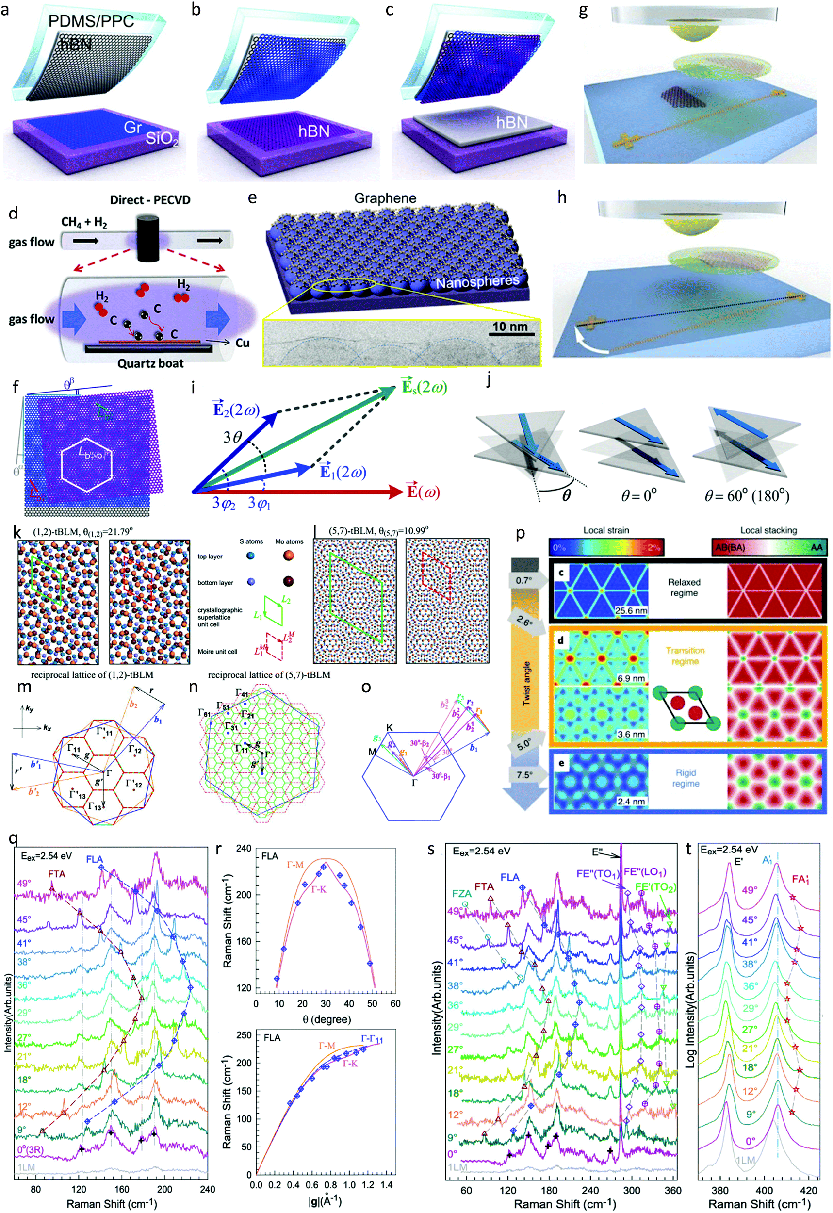 | ||
| Fig. 1 Moiré patterns and moiré phonons in vdW-twisted materials. (a–c) Schematic illustration of vdW assembly process to fabricate twisted Gr/hBN heterostructure and encapsulation by hBN. Reprinted with permission from ref. 61 Copyright 2019, AAAS. (d) Schematic drawing of the PECVD process adopted by Chen et al. to prepare large-area moiré heterostructures. Reprinted with permission from ref. 68 Copyright 2020, Elsevier. (e) Diagram showing nanosphere systems containing graphene. Top panel represents graphene deposited on hcp-SiO2 nanospheres (NS). Bottom panel magnifies a cross-sectional bright field scanning transmission electron microscopy image of graphene on 20 nm NSs. Reprinted with permission from ref. 74 Copyright 2018, the American Chemical Society. (f) Schematic view of two individual moiré patterns and super-moiré patterns for three overlapping hexagonal lattices. Reprinted with permission from ref. 61 Copyright 2019, AAAS. (g) Characterization of twist angle using a metallic line deposited on the substrate and hemispherical handle. Reprinted with permission from ref. 78 Copyright 2017, Proc. Natl. Acad. Sci. U. S. A. (i) Illustration of vector superposition of the second harmonic (SH) electric fields, where E1(2ω) is the electric field of the fundamental light, E1(2ω)[E2(2ω)] is the SH electric field from flake 1 (flake 2), and Es(2ω) is the resulting SH electric field from the stacking region. (j) Schematic of stacked bilayers with an arbitrary stacking angle θ, θ = 0° and θ = 60° (or θ = 180°). Reprinted with permission from ref. 78 Copyright 2017, the American Chemical Society. (k and l) Crystallographic superlattices and moiré unit cells of (k) (1, 2)-tBLM and (l) (5, 7)-tBLM with twist angles of 21.79° and 10.99°, respectively. (m and n) Reciprocal lattices of (1, 2)-tBLM and (5, 7)-tBLM, where the orange and blue hexagons represent the first Brillouin zone of the bottom- and top-layer MoS2, while the green and red hexagons demonstrate the reciprocal lattices of the crystallographic superlattices and moiré unit cells, respectively. Reprinted with permission from ref. 83 Copyright 2018, the American Chemical Society. (o) Calculated patterns of local strain and stacking in bilayer MoS2. Reprinted permission from ref. 84 Copyright 2021, Springer Nature. Moiré basic vectors of tBLM with twist angle θ < 30°. (p) Twist angle-dependent Raman spectra of tBLM under laser excitation of 2.54 eV. (q and r) Raman shifts of FLA modes as a function of twist angle θ and moiré basic vector |g|. (s and t) Raman spectra of tBLM in both low and high frequency regime. Reprinted with permission from ref. 83 Copyright 2018, the American Chemical Society. | ||
CVD growth is another promising alternative to mechanical exfoliation for fabricating smooth and reliable moiré patterns. Fig. 1d shows a schematic of the plasma-enhanced CVD (PECVD) process used by Chen et al. to grow large-area twisted bilayer graphene, where the growth was done directly on Cu foil and millimetre-size samples were achieved.68 Other researchers have also used a similar CVD growth technique to realize a wide range of 2D materials with enormous surface areas, which cannot be accomplished through mechanical exfoliation.69–73 Furthermore, they discovered that the pressure ratio between the flowing reactant gases CH4 can affect the twist angle to a significant extent. Patterned substrates can be manifested as another remarkable technique to produce moiré heterostructures. Specially designed nanospheres or micro-patterns can be fabricated on substrates, resulting in a periodic pattern. Transferring 2D materials on the periodic substrates can also lead to the formation of a moiré superlattice, as reported by Zhang et al.74–77 (Fig. 1e).
The characterization or correctly determining the twist angle is of utmost importance to properly judge the effect of the moiré pattern on the physical and molecular properties of materials. Hence, multiple methods have been developed and adopted over the past few years to measure the stacking angle with the lowest error. Primarily, most researchers use the edge angle of each layer to determine the relative twist, where microscopy and SEM images are employed for this purpose, as depicted in Fig. 1f.61 Other groups devoted further efforts and developed a more efficient method, which involves depositing a metal ruler on the substrate to measure the controlled twist angle78 (Fig. 1g and h). However, both methods suffer from an uncertainty of up to 1° due to obscure images, which make it difficult to identify the monolayer boundaries. Hence, more reliable approaches are essential to measure the twist angle. This led to the addition of a non-invasive optical mechanism in characterizing moiré patterns, such as Raman spectroscopy and second harmonic generation (SHG). Raman spectra collect extensive amount of data, especially the relative intensity ratio of different signature modes at various polarization of the incident laser. This can be utilized as a function of the twist angle to decrease the error in detecting the relative stacking angle between monolayer constituents.68 In addition, scanning tunnelling microscopy (STM), with resolution at the atomic level, can also assist in reducing the uncertainty. The SHG method has been widely adopted by several researchers in determining the crystallographic orientation of materials.79,80 It can decouple the coherent superposition of SHG signals obtained from each monolayer constituent, and this decoupled signal from the bottom and top layer can provide significant information on the twist angle. Therefore a combination of both Raman and SHG spectroscopy (Fig. 1I and j) can significantly decrease the uncertainty of the measured twist angle to around 0.01°,63,79,81 which is imperative to comprehend the emerging properties in twisted bilayer samples.
Moiré phonons
MSL has been known to exist in few-layered TMDC and its heterostructures in addition to conventional graphene and graphene-based bilayer structures. Complex molecular bonding and lattice arrangements lead to the formation of a distinct superlattice structure. This gives rise to special features and spectral properties that can be detected through numerous characterization techniques, for instance, moiré excitons, band structure, topological transitions, and most importantly moiré phonons, which appears to be very sensitive to the periodic modulation.The unit cell of the moiré superlattice in few-layered TMDC and heterostructures are often different and modified compared to monolayer TMDC; hence, they exhibit modified phonon properties, resulting in remarkable contrast in non-linear optical spectroscopy especially Raman spectroscopy. Moiré phonons are commonly referred to as phonons arising from modulated moiré patterns. The simplest prototype to investigate these features is bilayer MoS2, where twisted MSL results in differences in phonon properties. Twisted bilayer MoS2 (tBLM) was probed and investigated in early 2016, which lead to the observation of multiple new vibrational peaks in Raman spectroscopy. Specifically, low frequency shearing and breathing modes were clear evidence of the strong interlayer interaction and formation of a moiré pattern.82 Further theoretical analysis and experimental outcomes in tBLM related to moiré phonons were reported by Lin et al.83Fig. 1k and l present the crystallographic superlattice and moiré patterns of tBLM, as an example, with two distinct twist angles of 21.79° and 10.99°, respectively. They exhibit very different reciprocal lattices, as depicted in Fig. 1m and n, respectively. Paired prime numbers (m, n), where m and n are unequal, can be employed to represent the crystallographic superlattices with multiple stacking angles of tBLM, and the resulting lattice constant can be depicted by  , whereas for the MSL, the lattice constant translates to
  . This means that L and LM can be equal when |m − n| is equal to one. Therefore, (1, 2)-tBLM (θ(1,2) = 21.79°) shows equal lattice constants for the moiré unit cell and crystallographic superlattice; in contrast, (5, 7)-tBLM (θ(5,7) = 10.79°) manifests a variation in the lattice constants for the two unit cells (Fig. 1k and l). Eventually the structures transform into the same Wigner–Seitz cells of reciprocal lattices equivalent to the crystallographic superlattice and moiré lattice of (1, 2)-tBLM; however, they are disparate in (5, 7)-tBLM (Fig. 1m and n). When the twist angle is less than 30°, the difference between the basic vectors of the top and bottom reciprocal lattices is equal to the basic vectors of the moiré reciprocal lattices (Fig. 1o). Therefore, Raman spectroscopy can be directly employed to explore the phonic signatures that result from the folding and overlapping of phonons in the centre of Wigner Seitz cells at the centre of the Brillion zone.27Fig. 1p demonstrates simulated images of the atomic reconstruction that would result in a moiré pattern using the same platform of tBLM.84 The prevailing completion between the strain and interlayer coupling dominates the emergence of the periodicity. Researchers highlighted the existence of three possible molecular states, namely the relaxed and rigid regime with a transition state between which greatly alters the moiré unit cell and alters the favourability of the stacking configuration. This implies that strain is also a prominent factor affecting the moiré pattern, thus increasing the complexity in assigning and determining the phonon peaks that cause variations in the atomic configuration and local strain, which are both expected to stimulate the lattice vibration.84
Fig. 1q shows the Raman spectrum from the bilayer MoS2 interface investigated by Lin et al.83 for various twisted samples. The folded transverse acoustic (FTA) and longitudinal acoustic (FLA) phonons exhibit a similar gradual shift with an increase in the twist angle and a quadratic dependence. When the twist angle increases beyond 30°, the FTA and FLA modes demonstrate mirror symmetric behaviours (Fig. 1r and s, respectively). In addition, the twist-dependant FLA mode positions can vary between double segments of longitudinal acoustic (LA) phonon dispersion in atomically thin MoS2 projected towards the Γ–M and Γ–K directions. The FLA mode positions show a similar distribution between the Γ–M and Γ–K branches due to the fact that the basic vectors of the moiré reciprocal lattices are dependent on the twist angles (Fig. 1r). In every phonon branch of tBLM, there still exists six moiré phonons due to the similar reliance between the twist angle and basic vectors of the moiré reciprocal lattice. These phonons can degenerate to one folded mode similar to the FLA and FTA modes regardless of the interlayer interaction.83Fig. 1s and t show the moiré phonons observed in tBLM related to other phonon branches in addition to the LA phonon branch. The prominent peaks at 385 and 405 cm−1 are attributed to the non-folded E12g and A1g modes; in addition, the second order Raman modes of A1(M)–TA(M) can also be observed in tBLM. The E′′(Γ) mode is related to the degenerate LO and TO phonons at the zone centre, and hence is Raman active and absent in the monolayer constituent in the backscattering configuration. Due to the very complex nature of moiré patterns, it is very difficult to assign any peak to a phonon for bilayer TMDCs, where the complications increase in the case of folded modes that are more dependent on moiré superlattices. Furthermore, moiré phonons become difficult to investigate in thin layered TMDCs (more than two layers) and their heterostructures due to their intensely complex superlattice unit cell and computational models. However, a few experimental works have emerged in this field to help further understand moiré phonons, where in all cases, Raman spectra remain inevitable to identify any changes and modes related to the MSL.
Over the past few years, the platforms to scrutinize moiré phonons have been extended to a few other TMDC with remarkable phononic responses probed through Raman scattering. Advancements in high-density optical filters and attenuators have made it significantly convenient to observe low frequency breathing and shearing modes in Raman spectra, where researchers have also used them as a sensitive probe for the twist angle. Fig. 2a and b show the low-frequency Raman spectra of twisted bilayer WSe2 as a function of twist angle recorded by Lin et al.85 The interlayer breathing modes depict a strong scattering signature and shift in position with an increase in the stacking angle. The dependence of the breathing mode on the stacking angle, as summarized in Fig. 2a, has been found to match coincidentally with the calculated moiré period. Fig. 2c extends the Raman spectrum of bilayer WSe2 to a broader frequency regime, indicating multiple peaks besides moiré phonons. The majority of them are related to the LA and TA phonons of the twisted bilayer WSe2. Nevertheless, the appearance of moiré phonons in Raman spectra is considered direct evidence of MSL and the shifting of the phonon bands with twist angles further implies the sensitivity of the breathing modes to MSL. Evidence of atomic reconstruction is conceived at a twist below 3°, where shear modes are dominant in addition to breathing modes.
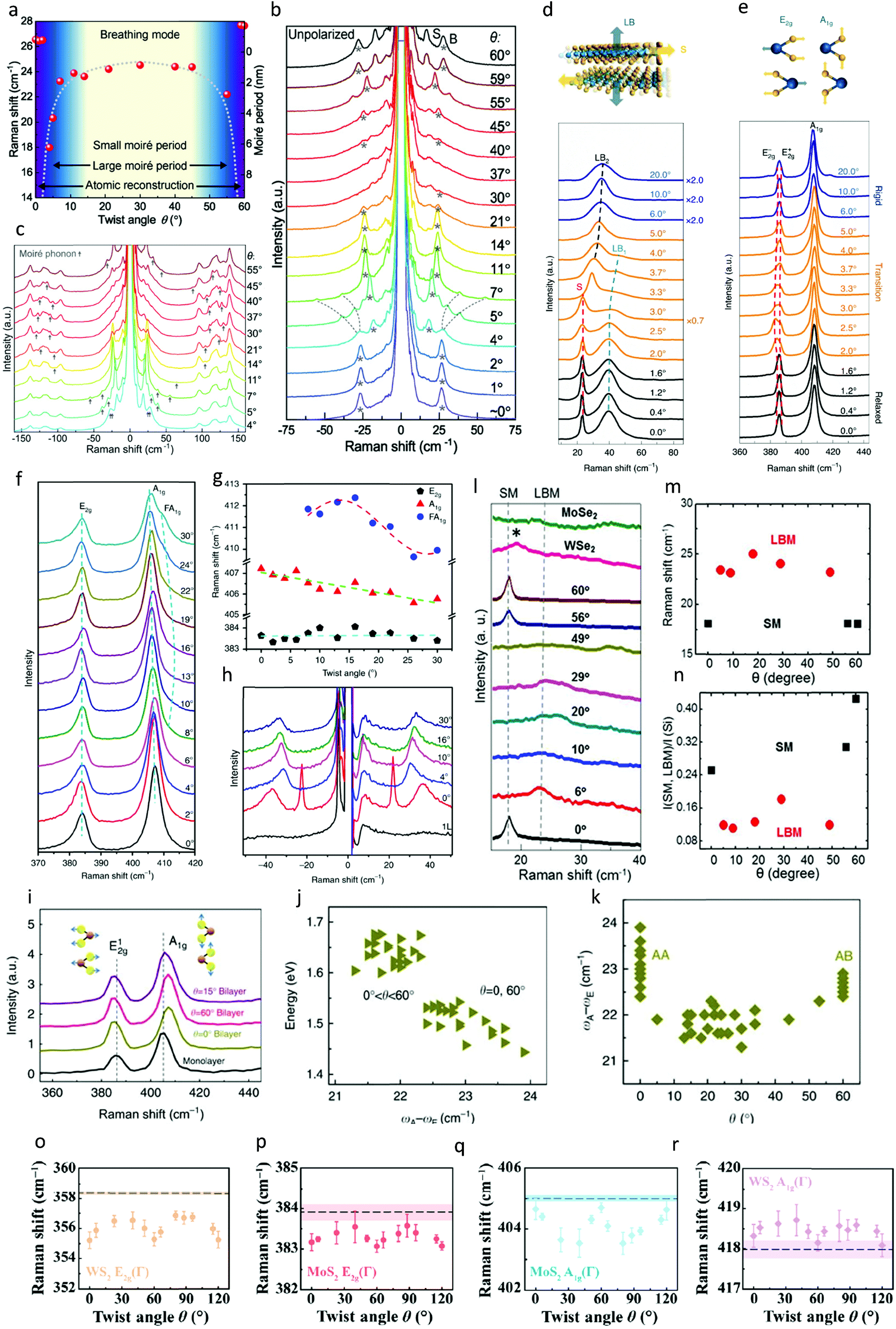 | ||
| Fig. 2 Raman signatures of moiré phonons. (a) Twist angle dependence of the breathing mode frequency identifying three regions: small moiré period, large moiré unit cells and atomic reconstruction. (b and c) Raman spectrum of twisted bilayer WSe2 as a function of twist angle, for (b) low and (c) high frequency regime. Interlayer breathing modes are marked by asterisks and moiré phonons are indicated by dashed line. Reprinted with permission from ref. 85 Copyright 2021, Wiley-VCH GmbH. (d and e) Interlayer and intralayer phonon modes from twist bilayer MoS2, respectively. Interlayer vibration results in the S and LB mode, while the intralayer mode conceives the E12g and A1g peak, including doublet splitting due to strain. Reprinted permission from ref. 84 Copyright 2021, Springer Nature. (f) Raman spectra from a series of MoS2 films with varying twist angles. (g and h) Position and intensity of E2g, A1g and FA1g peak as a function of twist angle. Dashed lines are either linear and sinusoidal or exponential fitting. Reprinted with permission from ref. 92 Copyright 2020, Springer Nature. (i) Characterization of interlayer mechanical coupling in twisted MoS2 bilayer using Raman spectrum from monolayer and bilayer twisted samples. Raman spectra of an MoS2 monolayer and bilayers with twist angles of θ = 0°, 15° and 60°. (j) Raman peak separation between the A1g and E2g (ωA − ωB) in MoS2 bilayers with different twist angles, which is the largest for AA or AB stacking and nearly constant for other twist angles. (k) Relation between Raman peak separation and PL peak. Reprinted with permission from ref. 94 Copyright 2014, Macmillan Publishers Limited. (l–n) Low-frequency Raman signatures on MoSe2/WSe2 heterostructure, focusing on the breathing and shearing mode. Reprinted with permission from ref. 95 Copyright 2017, the American Chemical Society. (o–r) Summary of E2g peak and A1g peak dependence on twist angle in WS2/MoS2 twisted heterostructure. Error bars are obtained from fitting and statistics. The horizontal dashed lines and shaded areas represent the average value and standard deviation of the initial peak positions of E2g and A1g of pristine monolayer MoS2 and WS2, respectively. Reprinted with permission from ref. 96 Copyright 2021, Springer Nature. | ||
Emergence of moiré patterns also effects the common vibrational modes relating to the in-plane and out-of-plane vibration, as evidenced by Quan et al.84Fig. 2d and e represent the Raman spectra of a twisted MoS2 homostructure divided into a low and high frequency regime. Here, the researchers accommodated the effect of strain in addition to the periodic modulation to meticulously investigated the occurrence of moiré phonons. The low frequency regime exhibited interlayer shearing and breathing modes, where the relative motion of the individual monolayer is parallel and perpendicular to the 2D layers, respectively.86–89 Interestingly, the two dominant intralayer modes in the high frequency regime showed twist dependence, in particular the in-plane mode. The E2g mode, originating from the in-plane vibration of sulphur atoms, evolved into a doublet between 2° and 6° twist, providing direct evidence of atomic reconstruction. The local strain evolves from this type of moiré pattern in a transition regime (Fig. 1p), which can distort the hexagonal unit cell and disrupt the three-fold rotational symmetry, causing mode splitting.90,91 They further utilized piezo microscopy measurements (PFM) to confirm the presence of the MSL structure.
Although the vdW technique provides the cleanest and pristine interface to analyse moiré phonons, advanced CVD techniques and transfer methods can be manifested to realize this type of nano-engineering at the atomic level. The epitaxial growth technique allows the fabrication of large-area MoS2 homostructures and trilayer junctions, which demonstrate similar moiré patterns. Lia et al. observed the alluring dependence of the out-of-plane mode (A1g) on the twist angle in CVD-grown samples92 (Fig. 2f–h). Interlayer vdW interactions and long range coulombic interaction account for the distinct angle dependence of the A1g peak. In addition, interlayer coupling was determined to be the strongest at near-zero twist based on the softening of the A1g phonon with an increase in the twist. Moiré phonons were also observed in these CVD-grown samples, originating from the off-centre phonons of the monolayer linked with lattice vectors of the moiré reciprocal space.83 Researchers also recorded a gradual change in the intensity of the Raman peaks with the twist angle, which was attributed to the stronger electron phonon coupling.93 However, Liu et al. recorded a slightly different response in twisted MoS2 bilayers grown by CVD (Fig. 2i–k). Albeit no intensity variation in the Raman modes was observed with the twist, interesting blue- and red-shifts were detected for the E12g and A1g modes, respectively.94 This twist dependence of the Raman modes provided an excellent platform to investigate the interlayer mechanical coupling strength. The separation between the E12g and A1g peak was used to characterize the effective interlayer coupling strength, where stronger coupling resulted in further separation. The investigation of 44 twisted MoS2 samples (Fig. 2j) revealed that the mechanical coupling follows a similar pattern to that of electronic coupling as a function of twist, where the small twisted samples manifested the strongest coupling.
The marvels of moiré phonons have also been extended to other material systems involving different TMDC and their heterostructures. Nayak et al.95 examined the effect of coherently stacked angles in the MoSe2/WSe2 bilayer system, as summarized in Fig. 2l–n. The Heterostructures with twist angles close to 0° and 60° exhibit shear modes in their Raman spectra due to the high symmetry stacking configuration, whereas that with intermediate angles manifests layer breathing modes owing to the mismatched atomic alignment.95 Similarly, low-frequency modes show greater sensitivity to the twist and interlayer stacking than the high-frequency E12g and A1g, peaks which appeared to be almost independent of the stacking angle and yielded less information. However, in the MoS2 and WS2 heterostructure, shifts and linewidths in the E2g and A1g phonon modes were found be twist angle-dependant by Wu et al.96Fig. 2o–r summarize the evolution of the in-plane and out-of-plane mode as a function of twist for both MoS2 and WS2 in the vdW heterostructure. Noticeably, the E2g mode was softened by up to 2 and 0.6 cm−1 in the heterostructure for WS2 and MoS2, respectively, when the twist was close to 0°, 60°, or 120°; in contrast, the A1g mode softened by 1.5 cm−1 and stiffened by 0.7 cm−1 for the 30° and 90° twisted samples. In these cases, carrier doping and charge transfer had a drastic effect due to the band alignment, which mainly modulated the dynamics of the A1g peak.96,97 Researchers have also made similar observation regarding the interlayer mechanical coupling strength, which was significantly dependant on the twist. The separation in peak position between E12g and A1g was utilized to depict this behaviour, which was attributed to the space-related repulsion between the sulphur atoms.
Nano-engineering based on a simple variation in stacking angle can result in immense change in the physical and mechanical properties of materials, where moiré phonons are an integral part to widen the aspect of studying the dynamics of twisted samples. Raman scattering investigation in twisted heterostructures have recently expanded to a wide variety of systems, mainly focusing on phonon-based interlayer interactions. This implies the importance of the resulting commensurate patterns and diverse modulation of the molecular and atomic arrangements in moiré heterostructures, which can have a variety of applications. For instance, moiré structures can be strong candidates for building photovoltaic devices or emitters due to the high binding energy of their interlayer excitons and their long lifetimes.12,98 MSL can have potential applications in valleytronics because moiré structures affect the topological order in TMDC monolayers and form a densely arranged 1D array. These helical channel arrays can transport valley currents.12,99 In addition to optoelectronic and electronic devices, amazingly these stacked heterostructures can also be applied as lubricants. Technological advances have confirmed that moiré patterns can introduce superlubricity and are robust to angle modulation of the stacking angle in a wide range.100,101 The ultralow friction in twisted bilayer graphene has been experimentally confirmed.102 These applications in the mechanical sector will be life changing and drastically beneficial to daily life.
Topological nanostructures and strain induction
One of the most common methods of inducing strain in 2D materials is through the formation of nanostructures such as wrinkles, leading to rough structures, which exhibit novel physical properties compared to their flat counterpart. Wrinkle engineering is a powerful and competent tool to tune electronic properties such as the energy gap of 2D materials and planar mobility of electrons.103–106 In addition, their optical properties can be also heavily manipulated such as PL, Raman spectra and second harmonic generation (SHG). Furthermore, wrinkles significantly improve the flexibility of materials including their twist, bending and stretchability.107 Therefore, multiple methods for the fabrication of wrinkles have been investigated to induce strain in atomically thin layered materials. Although some methods induce random wrinkles, others can generate controlled wrinkles, which usually involves transferring 2D materials to secondary substrates that possess ordered microstructures. Additionally, pre-stretched polymers and thermally induced shrinkable substrates can also induce patterned wrinkles.108–110 Flexible substrates can also generate ordered wrinkle structures by just bending or as a result of the mismatch of elastic modulus and thermal expansion.35 Based on the architecture of wrinkles, the mechanical, electrical, thermal and optical properties can be facilely tuned.
Fig. 3a and b present a schematic outline and route for the formation of patterned wrinkles in flexible and bendable substrates. ReSe2 and InSe were primarily used as the model platform by Yang et al.111 and Zhao et al.,112 respectively, to achieve patterned wrinkles in layered compounds. The PDMS substrate is commonly used, which can be pre-stretched before transferring the 2D material.39,112,113 Consequently, when the prestrain is relieved, periodic wrinkles in 2D materials are generated along the direction of the initial strain axis. This happens as result of the buckling-induced delamination resulting from the differences in both elastic modulus and ability of the 2D material and PDMS substrate to recover (Fig. 3b). The prestrain can be mathematically defined as114 , where L and ΔL correspond to the initial and stretched length of the PDMS substrate, respectively. However, it is important to note that the formation of 3D wrinkles can be induced if the prestrain is inserted simultaneously along the x and y directions of the substrate. When this type of prestrain is applied in multiple directions and released, it causes crumpling of the adhered 2D materials and provokes the formation of 3D wrinkles.115 A similar alternative to produce wrinkled nanostructures in 2D materials, besides pre-stretching flexible substrates, is by transferring 2D materials to the topmost surface of a pre-bent PDMS substrate. This installs uniaxial compressive strain when the prestrain is released (Fig. 3a). The maximum induced strain, ε, on top of the wrinkle can be computed theoretically as follows:13,116
 , where δ and λ are the height and width of the wrinkles, respectively, h corresponds to the thickness of the 2D material and σ is Poisson's ratio. The basic parameters can be obtained from AFM topography or SEM images. Fig. 3c shows the optical image and AFM image of InSe wrinkles and the SEM image of ReSe2 wrinkles is shown in Fig. 3d, where both images provide detailed information on the material topography.
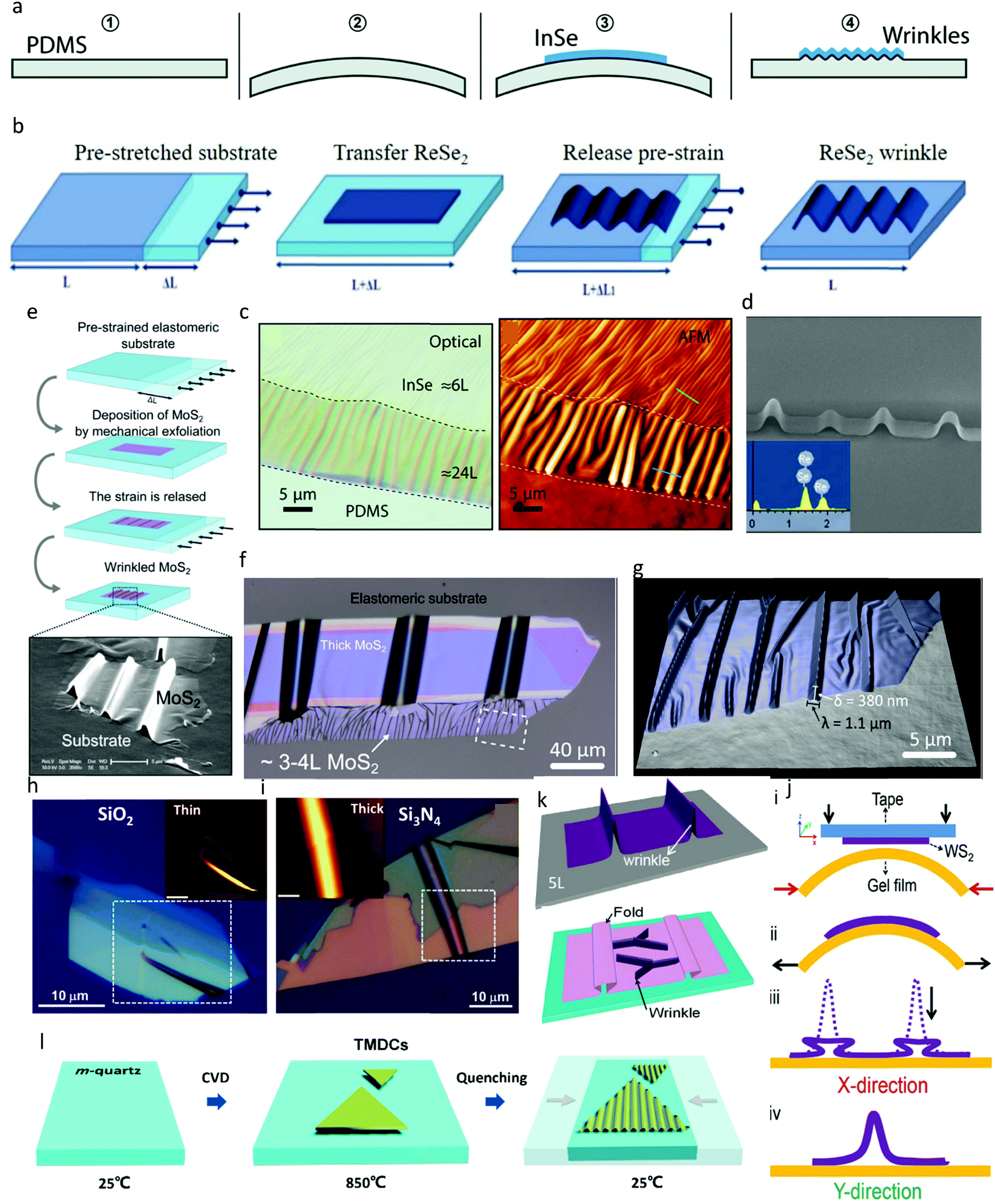 | ||
| Fig. 3 Nanostructure and wrinkle fabrication. (a) Step-by-step process of forming wrinkles in InSe using a pre-bent PDMS substrate. Reproduced with permission from ref. 111 Copyright 2019, The Royal Society of Chemistry. (b) Wrinkle formation in thin ReSe2 layers using pre-stretched PDMS substrate. Reprinted with permission from ref. 112 Copyright 2015, the American Chemical Society. (c) Optical microscopy image in transmission mode and surface topography of InSe2 wrinkles, respectively, showing the uniform Gaussian-like structure of the strained regions. Reprinted with permission from ref. 111 Copyright 2019, The Royal Society of Chemistry. (d) Scanning electron microscopy (SEM) image of ReSe2 wrinkles. Inset shows the energy dispersive X-ray spectrum (EDX) of ReSe2. Reprinted with permission from ref. 112 Copyright 2015, the American Chemical Society. (e) Schematic diagram of the fabrication process of wrinkled MoS2 nano-layers to induce localized uniaxial strain. An elastomeric substrate is stretched prior depositing MoS2 by mechanical exfoliation. The strain is released afterward, producing buckling-induced delamination of the MoS2 flakes. (f) Optical microscopy image of wrinkled MoS2 flake fabricated by buckling-induced delamination. (g) AFM topography image of the region marked by the dashed rectangle in f. Reprinted with permission from ref. 39 Copyright 2013, the American Chemical Society. Optical images of MoS2 wrinkle on (h) SiO2 substrate and (i) Si3N4 substrate. Inset shows the AFM image of the respective wrinkles. Reprinted with permission from ref. 120 Copyright 2017, the American Chemical Society. (j) Schematic diagram of fabricating wrinkles using mechanical buckling of PDMS substrate. (k) 3D representation of strained sample wrinkles and fold. Reprinted with permission from ref. 121 Copyright 2020, Wiley VCH. (l) Schematic outline of the route for the fabrication of wrinkle arrays in CVD-grown WS2. Reprinted with permission from ref. 124 Copyright 2021, the American Chemical Society. | ||
Gradually, the research into strain induction and nanostructures has been extended by multiple groups to other 2D materials and TMDC systems. Well-aligned wrinkles were generated in MoS2 flakes using an elastomeric substrate by Gomez et al.39 (Fig. 3e). They found that large-scale wrinkles were generated and were reproducible using this method. Fig. 3f and g show the optical and AFM images of the wrinkle MoS2 induced on different layer numbers, from the bulk to nanoscale regime, respectively. They also found that in monolayer and bilayer, the wrinkles tend to collapse and form folds due to their instability. It is worth noting that wrinkles can also be randomly generated during the mechanical exfoliation of 2D materials due to their nonhomogeneous breaking forces. When the material size is large than 10 nm, it is more prone to produce wrinkles.117,118 Deng et al.119 manifested that smaller flakes with fewer wrinkles can be obtained if the tape is released at a slower speed. However, the dimensions of the wrinkles were affected by the interfacial adhesion energy, which can be measured by transferring the wrinkled flake to other substrates such as SiO2 and Si3N4.120Fig. 3h and i show wrinkled MoS2 on multiple opaque substrates, which allows nano-indentation and other characterizations to take place. Khan et al. provided another simple strategy to produce nano-wrinkles in TMDCs but the process is similar to the mechanical buckling of flexible substrates.13 They also confirmed that the stability of the wrinkles is higher in multilayer TMDCs (>4L), whereas in atomically thin layers, the wrinkles collapse to folds due to their bending rigidity. Fig. 3j outlines the fabrication process and Fig. 3k schematically models the folds and wrinkles that are consequently formed. Big wrinkles are able unable maintain their curvature, which collapse to form folds and are formed in the direction perpendicular to the compressive forces. Tiny wrinkles can maintain their curvature and are generated in the direction parallel to the compressive force.121
Wrinkles can also be generated during CVD growth and by altering the thermal parameters during the growth process. This mainly originates from the mismatch in the lattice coefficients between the growth of the substrate and TMDCs, where during cooling, thermal expansion takes place, which can generate wrinkle patterns.118 Large-area wrinkled MoS2 was synthesized on graphene substrates by Kim et al. and modulated by the grain boundaries and nucleation density of graphene, including its thickness.122 Patterned sapphire substrates can also generate wrinkle MoS2, where wrinkled thin films of MoS2 were deposited on patterned substrates using a high vacuum co-evaporation method,123 which also enabled the lateral periodicity of the film thickness to be tuned. Fig. 3l provides an illustration of producing large-area wrinkles in monolayer WS2, which were epitaxially grown on an m-plane single-crystal quartz substrate.124 Initially, monolayer WS2 was grown via the CVD process on m-plane quartz at a very high temperature (850 °C).125 Then, the high temperature of the furnace was quenched, which could provoke the formation of wrinkle structures in epitaxial WS2. Alternatively, if the cooling process was allowed to occur naturally, then flat samples would be achieved.124
Fig. 4 depicts some nano-indentations of wrinkles, which were imaged using AFM. Fig. 4a–h show some height profiles of the wrinkles, including their thickness in MoS2 flakes. It is imperative to transfer these samples to SiO2 or other similar substrates that allow this type of characterization. The cross-sectional line profiles illustrate the small height to width ratio and also show the smooth and symmetric nature of the wrinkles.120Fig. 4i shows an AFM of the wrinkles fabricated by Khan et al., which show a large height. The SEM image (inset) further confirmed that the wrinkles could maintain their curvature in thicker layers when exfoliated mechanically using a flexible substrate.13 In addition, the height of wrinkles varied significantly based on the layer numbers, as depicted in Fig. 4j. Fig. 4k and l depict the AFM and SEM image of the wrinkles in monolayer WS2 grown by CVD, respectively, where neighbouring wrinkles are separated by distance of about 3 μm, indicating a quasi-periodic mechanical trend. However, these nano-wrinkles in the monolayer exhibited a much lower height of about ∼5 nm, which is much smaller than that in few layers.13Fig. 4m–o show the AFM image of the wrinkles on WSe2 monolayer fabricated on a piezoelectric substrate. The profiles also indicate the Gaussian shape of the wrinkles, which are the typical and commonly observed geometry of this type of nanostructure.126 However, an uncontrolled exfoliation procedure can create other complex geometries, which may lead to different deformation behaviours.
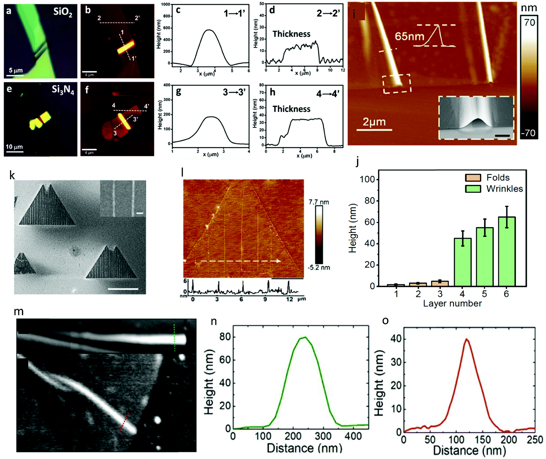 | ||
| Fig. 4 Nanoscale mapping of wrinkles and nanostructures. (a) Optical microscopy image of MoS2 wrinkled flake in SiO2 substrate. (b) Corresponding AFM image of the same flake. (c and d) Height profiles along the dashed lines in b, showing the profile of nano-wrinkles. (e) Similar microscopy image of MoS2 wrinkled flake on Si3N4. (f) Corresponding AFM image. (g and h) Height profiles along the dashed line in f upholding the wrinkle structure. Reprinted with permission from ref. 120 Copyright 2017, the American Chemical Society. (i) AFM image of wrinkles in WS2 thin layers. (j) AFM height deviation of wrinkles based on layer number. Smaller layers usually form folds. Reprinted with permission from ref. 13 Copyright 2020, the American Chemical Society. (k) SEM image of monolayer WS2 with aligned wrinkles epaxially grown on m-quartz. The bright contrast on the monolayer WS2 flake indicates the wrinkled array; the scale bar is 20 μm. The inset figure shows an enlarged SEM image of the wrinkle array with a scale bar of 1 μm. (l) AFM image of monolayer WS2 flake with aligned wrinkles. The scale bar is 6 μm. Line scan across the parallel wrinkles is shown below. Reprinted with permission from ref. 124 Copyright 2021, the American Chemical Society. (m–o) AFM images and height profiles of wrinkles in WSe2 monolayers. Reprinted with permission from ref. 126 Copyright 2019, the American Chemical Society. | ||
Strain-induced non-linear interaction
As mentioned earlier, the introduction of strain through wrinkles and nanostructures can significantly module numerous properties of a material. In particular, the non-linear interaction127 is significantly transformed under these strained conditions. Fig. 5a shows the Raman spectrum of MoS2 wrinkles and Fig. 5b and c depict the AFM and Raman mapping of multiple MoS2 wrinkles, respectively.39 The peak position of both the in-plane and out-of-plane mode are substantially shifted compared to their flat counterpart. In particular, the in-plane mode shows greater sensitivity to the uniform tensile uniaxial strain than the A1g mode, which is mostly related to the carrier doping.93,128 Liang et al. also investigated the non-linear optical properties of wrinkles in MoSe2, highlighted mostly by SHG.129 They calculated the amplitude of the strain directly from the curving geometry of the substrate (Fig. 5d) and monitored the strain primarily through the PL peak energy. Given that MoSe2 belongs to the non-centrosymmetric D3h point group, it emits a large SHG.80,130Fig. 5d and e show the SHG recorded with increasing strain from MoSe2, indicating that SHG is very sensitive to strain. In addition, normalized SHG provides a compelling linear fit to the strain amplitude, and also a platform to monitor strain amplitude. Fig. 5f shows the SHG intensity from the 2H bilayer region and monolayer region under strain. It establishes the fact the bilayer is much less sensitive to strain due to the low effective SHG, whereas the monolayer SHG increases rapidly under strain. A similar SHG analysis was also done on wrinkles in WS2 by Wang et al., where an 830 nm wavelength laser was used for excitation.124Fig. 5g–i show the SHG spectrum and mapping of a wrinkle in WS2, respectively, where the strained region exhibits a larger emission of second harmonics. An approximately 2-fold enhancement in SHG signal was obtained compared to the flat area. This amazing observation was attributed to the modified electric field in the wrinkle structure under the effect of strain.129Fig. 5j and k show the similar SHG maps recorded using a 900 nm femtosecond laser by Khan et al. In contrast, the wrinkles in 5L WS2 can undergo both an enhancement and quenching based on the wavelength of the excitation laser. They also resolved the anisotropic response of the wrinkle nanostructures by investigating the polarization-resolved SHG, where the distorted pattern obtained was explained using the photoelastic effect (Fig. 5l and m).131 It can be noted that the crystal quality of 2D materials and the complex morphology of wrinkles can provoke a variation in the characterization of the nanostructures in the same material.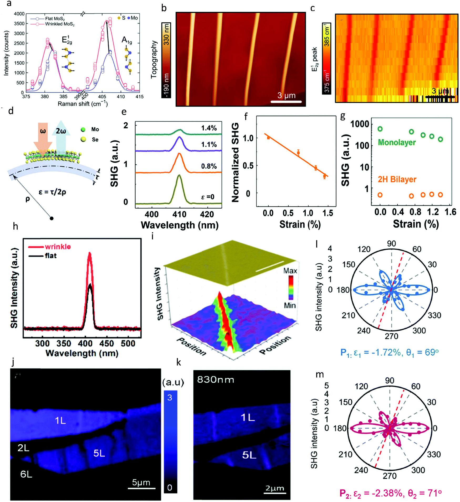 | ||
| Fig. 5 Non-linear optical characterization of wrinkle-based strained nanostructures. (a) Raman spectra of both the flat and wrinkled regions in vdW MoS2. Thickness is equivalent to 4 layers. Both in-plane E12g and out-of-plane A1g modes show a shift in Raman position toward a lower wavenumber; however, the in-plane mode exhibited greater sensitivity. (b) AFM topography image of wrinkles in MoS2. (c) Raman mapping of wrinkled regions showing the large shift in in-plane mode. Reprinted with permission from ref. 39 Copyright 2013, the American Chemical Society. (d) Illustration of the procedure used to apply strain in thin layers of MoSe2 by Liang et al. Arrows highlight the SHG process under uniaxial strain. (e) SHG spectra under increasing uniaxial strain. (f) Normalized SHG intensity as a function of strain. Straight line shows linear fit to the data. The error bars represent the standard measurement error from 12 samples. (g) Log plot of SHG intensity from monolayer or 2H bilayer MoSe2 as a function of strain. The negligible SHG response in bilayer reveals the perfect transfer of strain from the bottom layer to the top layer. Reprinted with permission from ref. 129 Copyright 2017, the American Chemical Society. (h and i) SHG spectra taken from the flat and wrinkled regions in WS2. Wrinkle WS2 exhibited a higher SHG. (i) SHG intensity mapping of wrinkles in WS2, showing an enhancement in wrinkles compared to the flat regions. Reprinted with permission from ref. 124 Copyright 2021, the American Chemical Society. (j) SHG map obtained using a 900 nm excitation laser for both flat and wrinkled regions in 5L WS2. (k) Similar SHG map but using 830 nm excitation. The change in excitation wavelength resulted in an enhancement and quenching in wrinkled WS2 regions. (l and m) Polarization-resolved SHG intensity corresponding to strained winkles in j and k, respectively. Fitted lines show the fitting to the experimental values, revealing a distorted pattern. Reprinted with permission from ref. 13 Copyright 2020, the American Chemical Society. | ||
Therefore, wrinkles have been accepted as the most straightforward way to induce strain in 2D materials and modulate their optical properties. Field-effect transistors (FETs) and photodetectors based on wrinkled nanostructures have already been demonstrated to show improved responses. Strained FETs show a higher mobility at 30 K, which is attributed to the reduced lattice and impurity scattering of the wrinkled regions. Photodetectors based on wrinkles show an enhanced photo-response due to their increased light absorption and indirect gap transition.119 The high stretchability of 2D materials realizes the dynamic tenability of these properties by stretching. Hence, flexible electronics based on wrinkle structures have attracted immense attention. Their applications have also extended to wearable electronic devices, artificial skins, panel displays, health surveillance, touch screen technology and environmental monitoring.132–138 Flexible energy sources and electrodes are also demanded when waterproof and anti-oxidation properties are required. It is expected that strained-based flexible devices will encompass a large sector of future low power household appliances. Derivatives of graphene with wrinkles have shown promising applications in intelligent devices, biomedicine and water treatment.139 Wrinkled graphene oxide serves as a remarkable biosensor, and in addition, due to its tuneable optics, it can modify transmittance by scattering light. In biotechnology, topological structures can assist as possible bacterial growth inhibitors,140 and also serve as promising alternative adsorbents for minimizing micro-pollutants in complicated water environments. Wrinkled graphene has been idealized as suitable electrodes in supercapacitors due to its increased surface area and reduced stiffness, while inhibiting stacking.141 Stretchable supercapacitors developed by stacking wrinkled graphene can be used in most electronic devices. In addition, wrinkled graphene can also be applied as a scaffold to attach nanoparticles for energy applications.142 Wrinkles have further attracted attention in field electron emission (FEE) cathodes. Topological structures in layered materials, which also offer ultralow thickness and high transparency, are attractive emitters for application in FEE.103 In summary, 2D materials with wrinkled nanostructures should be selected based on the application.
Substrate modulation: trenches and microcavities
The dielectric environment is a very sensitive factor to regulate various properties of 2D materials and is critical for judging device performances. Freely standing and suspended nanomaterials provide greater potential for exploring innovative physical phenomena and allow more avenues for applications such as NEMS-based sensors. Engineering the substrate to reduce dielectric screening and suspending the 2D material eliminate substrate interaction and provide a greater degree of freedom for motion when excited by a laser. In addition, it also increases their thermal isolation and results in novel changes to optical properties and thermal conductivities, where Raman spectroscopy is a fundamental examination tool. Hence, multiple attempts have been made to engineer substrates in the nanoscale regime, including uniquely designed trenches, microcavities and pre-patterned holes, and to create freestanding 2D materials, numerous transfer techniques have been adopted and implemented.Fig. 6a shows a schematic outline of the fabrication of microcavities in the commonly used Si/SiO2 substrate. Bae et al.143 used photolithography and dry etching (inductively coupled plasma, ICP) to pattern microcavities on an Au-deposited Si/SiO2 substrate. Fig. 6b shows the cross-sectional SEM image of the patterned structure, indicating that the holes are 5 μm deep with a diameter of 3.5 μm. In addition, the bottom surface sustained a rough morphology, which assists in avoiding interference when a laser is reflected from it.143 Also, the edge of the cavity is relatively clean and sharp, which allows the contact between the Au film and 2D material to be conformal. Pei et al.44 also patterned circular holes on an Si/SiO2 substrate to reduce the dielectric screening on atomically thin MoSe2. As shown in Fig. 6c, 3 μm-deep holes were installed on the SiO2 substrate through plasma etching, thus achieving circular trenches with different diameters. 2L MoSe2 was eventually transferred using the vdW transfer method to the trenched substrate, after it was exfoliated mechanically, to obtain freestanding MoSe2. The corresponding PL mapping (Fig. 6d) implies that the suspended region exhibited greater photoluminescence owing to the dielectric reduction.
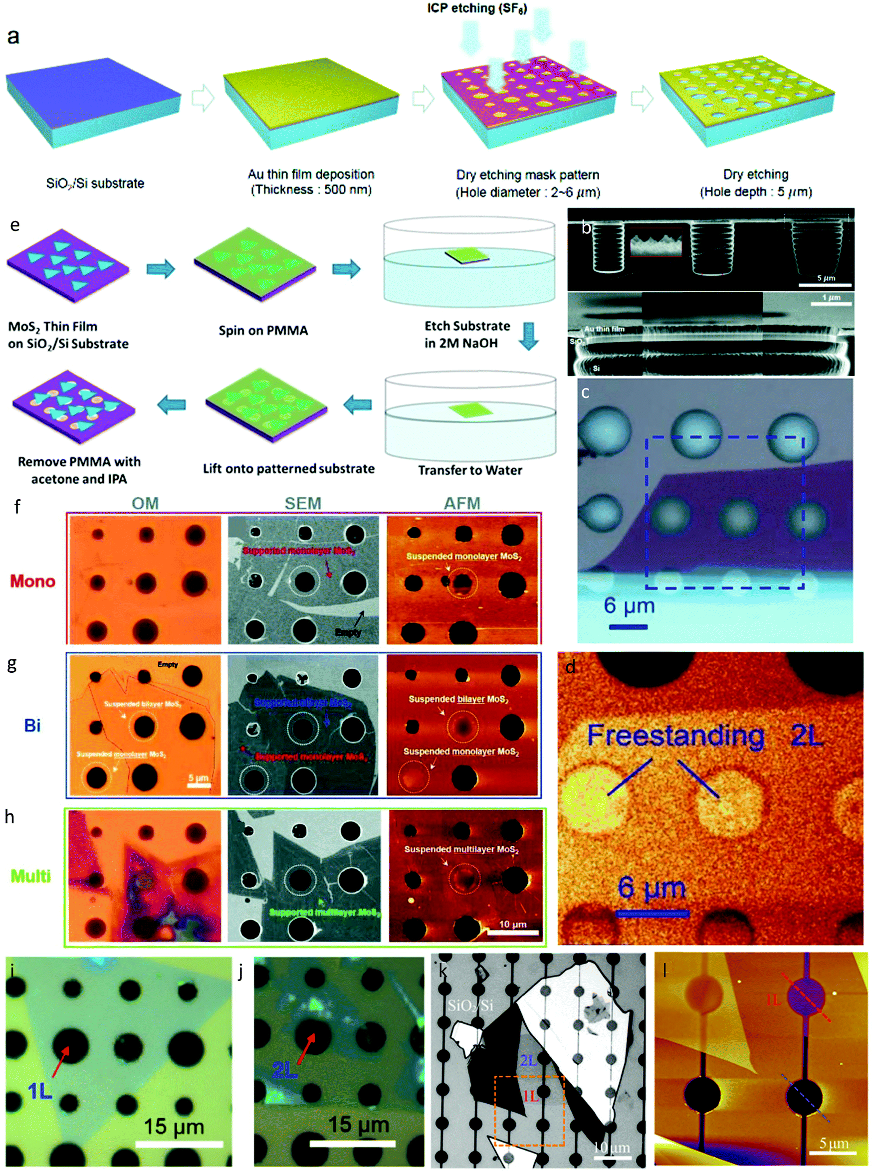 | ||
| Fig. 6 Substrate engineering in nanoscale regime. (a) Schematic outline of the process for the fabrication of Si/SiO2/Au substrate with microcavities or circular trenches. (b) SEM image of cross-sectional view, showing the trench. The inset shows the bottom surface of the microcavity, marked by the red dash line. Reprinted with permission from ref. 143 Copyright 2017, The Royal Society of Chemistry. (c) Top view of Si/SiO2 substrate with similar circular trenches or holes and bilayer MoSe2 transferred mechanically on the substrate. (d) PL mapping of freestanding 2L MoSe2, corresponding to the blue rectangular box in c. Reprinted with permission from ref. 44 Copyright 2017, the American Chemical Society. (e) Schematic of wet-transfer method to fabricate freestanding 2D materials. MoS2, grown by CVD, was transferred using a polymer support to pre-etched substrate. Reprinted with permission from ref. 45 Copyright 2017, Wiley-VCH. (f–h) Optical image, AFM topography and SEM image of suspended and supported monolayer, bilayer and multilayer MoS2 films, respectively. White dashed line indicates suspended regions of MoS2. Reprinted with permission from ref. 143 Copyright 2017, The Royal Society of Chemistry. (i and j) Optical image of freestanding 1L and 2L WS2 on Si/SiO2 substrate. Array of holes ranges from 3 μm to 6 μm in diameter. Reprinted with permission from ref. 144 Copyright 2015, Springer. (k and l) Optical and AFM images of 1–2L hBN on Si/SiO2 substrate with prefabricated micro-wells for fabricating freestanding samples. Reprinted with permission from ref. 146 Copyright 2019, AAAS. | ||
Although exfoliation and dry transfer are widely used for the fabrication of supported and suspended 2D materials, wet transfer has also gained momentum for achieving large surface areas and surface to volume ratios for suspended materials. Fig. 6e schematically depicts an example of the wet transfer process45 widely used for transferring CVD-grown films. Usually the 2D material, in this case MoS2, is grown beforehand using the CVD process on a normal SiO2 substrate. Then, a polymer is used to transfer the materials, where initially polymethyl methacrylate (PMMA) is spin-coated on the grown MoS2 and baked using a hot plate at high temperature for 5 min. It is also common to use a different polymer film than PMMA. Then, the films are dipped on 2 M NaOH at 80 °C, which causes the MoS2/PMMA film to detach from the substrate and float on the surface of the solution. Subsequently, the films can be cleaned using deionized water and transferred to another SiO2 substrate pre-patterned with holes and trenches. To allow the water to evaporate completely, the new substrate with transferred films can be placed in a desiccator for drying. Subsequently, the PMMA layer on top can be removed by immersing the substrate in a beaker containing acetone for 20 min. Further rinsing can be done by gradual immersion in a beaker of IPA and deionized water, and the films are eventually left to dry in a desiccator until all the solvents have evaporated. It may be important to note that adopting a gentler cleaning and lifting strategy for films assists in maintaining the structure and size of the as-grown materials because the wet transfer process has the tendency to drag the films down the hole or trenches.45 A similar process was used by Bae et al.143 to transfer MoS2 films on a pre-patterned Au substrate. Fig. 6f–h show the optical microscopy, SEM image and AFM topography of the different MoS2 layers transferred by the wet technique, respectively. Imaging techniques help to confirm the success of the transfer on prepatterned substrates. In addition, the images also ensure that the wet transfer technique works for all layer numbers, from atomically thin to multilayer.
Fig. 6i and j show suspended and freestanding samples of other TMDCs such as 1L and 2L WS2 grown by CVD and transferred by the wet method. The reactive ion etching technique was used by Peimyoo et al.144 to engineer the substrate and accomplish patterned holes. The as-grown WS2 was then transferred chemically to it. In this case, the researchers used 1 M potassium hydroxide (KOH) solution after spin-coating PMMA to detach the film from the substrate. However, KOH is a strong etching agent, which can easily erode the SiO2 epilayer, casing the chips to dissolve.145 This would leave the MoS2 and PMMA films floating on the surface. Furthermore, they removed the PMMA coating from the top by baking in an ultrahigh vacuum heater for 10 min instead of dipping in a beaker of acetone.145 Therefore, it is common to modify the steps of the wet transfer technique (shown in Fig. 6e) and implement different agents for each process. Due to the ease and precision of this process, it can also be used to fabricate suspended samples of other 2D materials. However, wet transfer involves the use of corrosive chemicals and the transferred samples are prone to contamination.146Fig. 6k and l show freestanding hBN on Si/SiO2, which was simply transferred using the dry method. Cai et al.146 highlighted the importance of contamination- and defect-free surfaces for characterizing other properties such as thermal transport. Thus, the absence of any polymer in the dry method caused the hBN sheets to be free from defects and grain boundaries.147,148
Substrate engineering through holes and trenches results in a significant variation in optical properties of layered materials. Both photoluminescence and lattice vibration undergo tremendous modulation when the dielectric screening is reduced. In addition, it can also trigger the mechanism of many-body interaction149–151 and lead to the emission of complex particles. Fig. 7a shows a schematic of freestanding 2L MoSe2 fabricated mechanically by Pei et al.44 and Fig. 7b shows the PL spectra taken from the suspended and substrate bound regions at 6 K. A new biexciton peak was observed from the freestanding region only, which is the result of binding trions and excitons. Reduced dielectric screening was key to this observation of many-body particles, which is also modified by the density of trion states and laser power. Fig. 7c–e show the Raman spectra in the high-frequency regime taken from the supported and suspended MoS2 layers. The obvious contrast between the individual spectra implies that the substrate can modulate the lattice symmetry and molecular vibrations.45 The shift in the Raman peak and change in mode intensities are prominent even in 5L MoS2. Brien et al. attributed this Raman shift to the induced strain in the MoS2 layers suspended over the holes; in addition, the lack of substrate inhibition also proliferated the out-of-plane motion of the layers, which further affected the intensity of the Raman spectrum.45
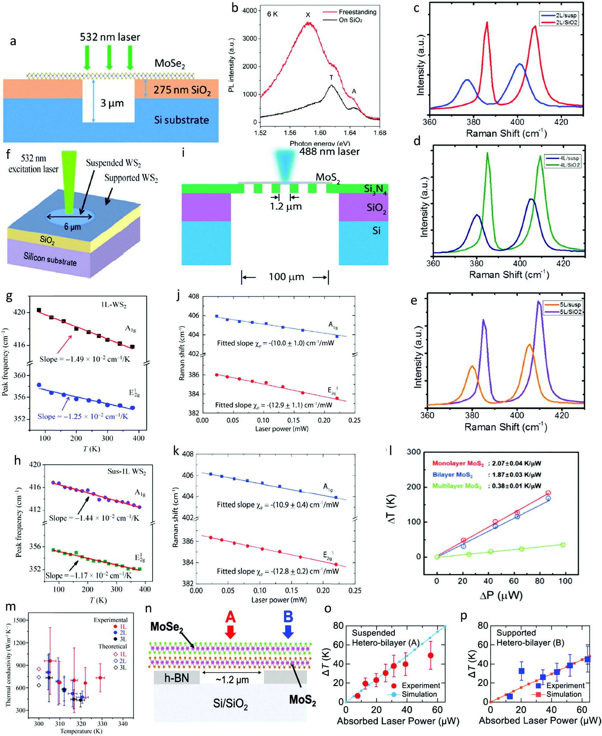 | ||
| Fig. 7 Non-linear characterization and thermal conductivity of freestanding 2D material. (a) Schematic view of freestanding MoSe2 bilayer used for optical characterization by 532 nm laser. The circular holes were pre-patterned before transferring the MoSe2 layer. Depth of holes is 3 μm. (b) Measured PL spectra from supported and suspended MoSe2 at 6 K. X marks the appearance of a new peak (biexciton) due to substrate modulation. Reprinted with permission from ref. 44 Copyright 2017, the American Chemical Society. (c–e) High-frequency Raman spectra obtained from both substrate-bound and freestanding 2L, 4L and 5L MoS2, respectively. Reprinted with permission from ref. 45 Copyright 2017, Wiley-VCH. (f) Schematic representation of suspended and supported WS2 on Si/SiO2 substrate prepared for Raman measurements using 532 nm laser excitation. (g and h) Temperature-dependant Raman spectra recorded experimentally from substrate-bound and suspended monolayer WS2, respectively. Thermal dependence of E12g and A1g peak movement is labelled, where the slope of A1g is more sensitive to the substrate. These measurements were eventually used for calculating the thermal transport in WS2. Reprinted with permission from ref. 144 Copyright 2015, Springer. (i) Schematic depiction of monolayer MoS2 on Si/SiO2/Si3N4 substrate. (j and k) Raman spectra recorded with increasing laser power for supported and suspended monolayer MoS2. Similarly, the A1g peak showed greater sensitivity to local heating from the laser. These measurements were used for calculating the thermal conductivity of MoS2. Reprinted with permission from ref. 152 Copyright 2014, the American Chemical Society. (m) Thermal conductivity of atomically thin hBN as a function of temperature. Reprinted with permission from ref. 146 Copyright 2019, AAAS. (n) Schematic cross-section of MoS2/MoSe2 heterostructure sample fabricated using Si/SiO2 substrate with pre-patterned holes to obtain suspended heterostructure. (o and p) Experimentally recorded rise in temperature, ΔT, with local laser heating from both supported and suspended heterostructure, respectively. Heat equation model was used for simulation. Thermal conductivity extracted was 115 W m K−1. Reprinted with permission from ref. 155 Copyright 2020, The Japan Society of Applied Physics. | ||
Suspended materials also respond differently when the thermal conditions are changed compared to supported materials. Therefore, temperature-dependant Raman spectroscopy is an integral platform to investigate the thermal transport and conductivity of layered materials. Fig. 7f shows a schematic of probing the atomic vibrations of layered WS2 using 532 nm laser excitation. Fig. 7g and h show the Raman spectra taken from supported and suspended monolayer WS2 as a function of temperature, respectively, where the A1g mode shows greater sensitivity to the substrate modulation though holes and microcavities. The slope for the E12g mode remained roughly constant with a variation in temperature due to the in-plane atomic vibration being less sensitive to the substrate. Finally, the calculated thermal conductivity (K) was 32 W (m K)−1 and 53 W (m K)−1 for monolayer and bilayer, respectively, at RT.144 This optothermal Raman method involving suspended 2D materials is indeed very common and can reliably estimate the thermal conductivity (K) and thermal expansion coefficient of layered compounds beyond graphene and TMDCs. Fig. 7i shows a similar assembly used by Yan et al.152 to characterize the lattice vibrational properties, and eventually thermal conductivity of atomically thin MoS2 using Raman spectroscopy. Fig. 7j and k show the Raman spectra of both supported and suspended MoS2 with an increase in laser power, which causes local heating. Similarly, the slope of the A1g peak is more sensitive to the local temperature rise from laser irradiation. The temperature and laser power coefficients of the Raman shift form the basis of computing the thermal conductivity by analysing the ΔT vs. ΔP curve, as shown in Fig. 7l. Usually, the A1g mode is used to calculate the thermal conductivity given that it is not sensitive to any strain effect.91 The thermal conductivity of monolayer MoS2 is 13.3 ± 0.3 W m−1 K−1, as recorded by Bae et al. at RT, which is slightly different from that of 34.5 W m−1 K−1 extracted by Yan et al., also at RT. Multiple works have used a similar approach to estimate the thermal transport of pristine 2D materials, which confirms the popularity of this method. However, the discrepancies between different reports can be attributed to the uncertainty in the Raman shift recorded from the measurement setup, leading to errors in the first-order linear coefficients.153 In addition, PMMA residue left on the sample surface and air surrounding the sample can also effect the extracted thermal conductivity value.154
The optothermal Raman method involving suspended materials has also been used to measure the thermal conductivity of different layered compounds. Fig. 7m shows the thermal conductivity of high-quality HbN obtained experimentally and using DFT simulations by Cai et al. Similar trenched substrates were used to record the phonon movement with temperature. As shown, the value of K deviated non-linearly with a change in the operating temperature. Also, K for hBN decreased with an increase in thickness.146 Mouri et al. characterized the thermal properties of a 2D heterostructure, where they fabricated a suspended heterostructure of 1L MoS2/1L MoSe2 encapsulated with hBN. Fig. 7n shows a schematic of the assembly and the ΔT vs. ΔP curves are presented in Fig. 7o and p. The supported and freestanding samples exhibited different gradients, where the latter was higher than the former. This implies that the samples transferred over the trenched substrate underwent rapid increase in temperature with local laser heating. The K of the hetero-bilayer was determined to be 115 (±25) W m−1 K−1 from the Raman scattering spectroscopy method.155 Understanding heat dissipation is crucial for applying 2D materials in future power electronic devices, where trenched substrates form the ideal platform for studying the thermal transport.
Future road map, challenges, perspective and conclusion
This review provided a comprehensive summary of three major techniques of nanoengineering in layered two-dimensional materials, which has far been heavily explored and scrutinized in the materials science community and received proliferated interest in the last decade. The stacking of two or mode layered materials at different twist, manufacturing nanostructures in 2D materials to induce strain and customizing the substrate provide a suitable platform to examine the fundamental physics, modulate the physical and optical properties and realize innovative devices. We focused mainly on the non-linear optical properties influenced largely by nanoengineering, such as Raman scattering and second harmonic generation, which have not been reviewed properly to date. Although there are multiple other methods to engineer 2D materials on the nanoscale, the methods discussed herein remain fundamental and straightforward to diversify the practical applications of layered compounds. However, few challenges still prevail among them, which still need to be addressed.It is evident that field of 2D material itself has substantial challenges, although it is dominating the landscape of nanotechnology and has made great strides. One major concern is the development of facile and low-cost fabrication methods for the synthesis layered materials on the wafer-scale with controllable thickness, which must be straightforward with minimum complications to meet the industrial demands. More investigations are needed on the surface science of 2D materials, which is directly related and immensely sensitive to their intrinsic characteristics; in addition, neighbouring material interfaces in heterojunctions and hidden substrates must also be examined thoroughly because in the atomic regime, most atoms reside at the surface.156 Voids, substitutional impurity and grain limits may act as extended flaws in 2D nanomaterials, where defective structures create leakage routes that limit the thickness of the material, and hence restrict its device applications.157,158 These flaws in nanomaterials including 0D points defects and dislocations, can also modulate their optical, electrical and mechanical properties.156 Growth and assembly methods that can regulate defective structures must be formulated with utmost priority. For emerging and new layered crystals, challenges remain in transferring the materials to nanopore chips or updating methods for growing materials over apertures for membrane applications.159 In terms of electronic devices, 2D materials are yet to be integrated into commercial integrated circuits (IC). Two vital challenges are manufacturing defect-free, ultra-thin, homogenous optical gate insulators that are excellent in quality and achieving restive elemental connections. In addition, reliable methods to create good dielectric layers using atomic layer deposition need further attention.
The area of moiré physics and moiré quantum materials is relatively new and the hunt for stable 2D materials needs to be investigated more thoroughly through encapsulation or interfacial engineering, without manipulating the twisted heterostructure. Also mechanical exfoliation is mostly used to fabricate moiré patterns, leading to a major challenge in designing large-area twisted heterostructure. The precision control of a small twist angle between two 2D materials, with diminished uncertainty remains a major goal for meticulously visualizing the MSL and characterizing quantum phenomena.160 Furthermore, it may also be alluring to investigate the role of defects, strain, nucleation density and doping in 2D materials in the architecture of MSL and related phenomena. Finally, to multiply the functionality of these materials, more research is required into the integration of moiré quantum materials in electronic and photonics devices. Nevertheless, vdW twisted heterostructures and moiré physics remain a promising area with a multitude of possibilities and unknown properties. Unconventional superconductivity and resonant tunnelling are among the exciting new phenomena observed in moiré materials. Further research can unveil more mysteries that still exist in the area of twisted materials. For instance, enhancing strategies and developing techniques to grow large-area twisted superlattices with in situ twist control and stability will further increase our understanding in this field. Also, increasing the ability to isolate, stack and dynamically rotate the twist angle in a wider range of 2D compounds and remodelling fabrication methods may lead to innovative applications in nanoelectronics, quantum physics, computing and communication.
Nano-manufacturing topological structures such as wrinkles in 2D materials is fundamental for the application of strain, which in turn significantly modulates different properties, photoelectricity in TMD and the energy band structure and electrical property.118 These strained nanomaterials act as a great resource for tuning interlayer coupling, fabricating hybridized functional materials, optical SHG and strain-tuneable single photon sources.119,126,161,162 However, it is a challenge to fabricate this type of topological structure in a controllable fashion, which has still eluded the scientific community. It is important and essential to develop fabrication methods for generating topological structures in a particular direction with a definitive location, dimension and density, which can significantly contribute to the magnetic, optical, mechanical and electrical properties. Prior reports have indicated that the wrinkles generated using pre-stretched elastomeric substrates are not controllable in any aspect and are also small; in addition, their fabrication is restricted to flexible substrates. Therefore, for practical applications, it is imperative that the methods for the fabrication of nanostructures can freely transfer them to any substrate. This will overcome their significant limitations in optoelectronic devices. Although 2D materials possess strong deformation capacity, the strain in 2D materials cannot reach the range predicted through simulations. One major reason for this may be the lack of understanding of the interfacial interaction strength between the substrate and material. Sometimes, strain may not be effectively conveyed to 2D materials. Therefore, it is imperative to further investigate the interfacial mechanical behaviour, particularly interface adhesion and friction behaviours, in relation to substrate and material. Furthermore, it may be of value to optimise existing methods or explore new methods for the application of strain, enabling even higher strain to be achieved in the future. It is worth noting that strain application has some limitations in modulating certain properties of 2D materials. For examples, strain in magnetic 2D materials has been mostly applied at the theoretical level, which is difficult in experiment, hindering spintronic applications. The next possible step in strain-based research is the analysis of the intrinsic character between the structure and property of 2D materials under strained conditions, which can lead to more breakthroughs in property modulation through strain and wrinkle formation.
Topological structures in 2D materials have been largely used in FETs and photodetectors and their usage can be extended to supercapacitors, electrodes, energy storage and memory resistance.103 TMDCs are a vital candidate in wearable and stretchable devices but their applications are limited due to their poor chemical stability and mechanical strength. Nano-engineering of TMDCs through their topological structure enhances the avenues for their applications in wearable electronics, given that the mechanically deformed wrinkles and folds are stable and can operate fully under strain. Although this field requires further research and development, wrinkled structures improve the ability of TMDCs to stretch, which diversifies their application fields to strain sensors, health monitors and electronic skins.118,163 Hence, it can be anticipated that strained 2D materials and their topological nanostructures provide new dimensions for applications in energy harvesters and wearable electronics. In the case of flexible device application, the feeble adhesion between the metal electrode and flexible substrate may be an issue in terms of device stability and longevity because it is easy for the material to fall off from the flexible substrate. Therefore, immense development of integration technology is the key to the more robust application of multifarious flexible devices.
Substrate modulation such as trenches and microcavities remains a popular method to tune the optical and electronic properties of layered materials. Different reports have implemented micropatterns and holes of various sizes, shapes and geometries in substrates. However, most studies remain limited to silicon oxide and Si substrates. It is important to extend these microcavities and nanopatterns to other substrates including transparent ones such as sapphire, glass, and quartz. Also, the materials used for photolithography and plasma etching must accommodate metal-plated Si substrates including, Au, palladium, Si3N4, and aluminium. Furthermore, challenges also persist when transferring 2D materials on top of the trenches and holes. Although vdW assembly is commonly and rapidly used, its yield and success rate are relatively low and samples are prone to breaking during the process. Also, the surface area obtained using this method is reduced, which impedes the practical application of suspended structures. Although the wet transfer technique provides a reliable alternative, it causes chemical contamination of the layered materials; in addition, remnant residues and deposits from polymers and etching agents can further modify the structural and chemical properties of the 2D materials. Hence, designing methods to generate large-scale suspended and freestanding 2D materials remains imperative for industrial applications. Multiple reports have provided proof-of-concept devices and NEMS sensors based on suspended 2D materials, where a large surface area may not be imminent. These nanodevices based on freestanding layered materials offer miniaturized dimensions, increased sensitivity and novel functionality compared to conventional silicon-based devices.14 However more research is required to extend NEMS devices to potential and more beneficial applications such as Internet of Things and autonomous mobility.
2D materials have emerged as the backbone of modern devices, which can meet multiple industrial demands, such as high-speed transceivers for information processing. Although silicon photonics can be greatly integrated into complementary metal oxide (CMOS) circuits, due to its low cost and high integratability it can suffer drawbacks such as difficulty to manufacture efficiently and complexity to detect and modulate in integrated silicon chips. Graphene, black phosphorus (BP) and TMDCs offer an alternate platform for real-life device applications, where multiple layered materials have been applied in optical communication,164 biosensing,165 laser sources,166 photodetectors164 and biomedical components.167 Given that these 2D materials can be easily transferred to integrated silicon chips, it allows them to be applied in high-speed silicon chips and telecommunication sectors.168,169 Other applications of 2D materials include waveguide-based hybrid structures, photonic crystal waveguides, microring resonators and plasmonic waveguides.170 It may be worth realizing the immense importance of layered materials in laser sources, where 2D material-based nanoscale lasers can operate at room temperature. For instance, monolayer and multilayer MoTe2 and MoS2/WSe2 heterostructures have been converted into laser devices,171,172 in addition to several other TMDCs. Furthermore, they are also good sources for single-photon generators and can overcome the drawbacks caused by conventional ones, for instance, quantum dot-based single photon sources suffer from weaker confinement and long spin coherence, which restrict their further development. TMDCs and hBN offer high-performing single photon generators that can be operated at RT.170,173 In addition to graphene, BP and TMDCs have been found to have remarkable application in telecom systems as optical modulators, which convert signals from the electrical to optical domain, forming the foundation of the signal processing chain.170 Due to their high carrier mobility and CMOS compatibility, 2D material-based devices meet the requirements of ideal optical modulators, i.e., large bandwidth and low energy consumption. Furthermore, layered materials have shown promising prospects in high-speed thermo-optic modulators.174 Also, state of art photodetectors have already been established using various 2d materials.170
Therefore, it is evident that nanoengineering 2D materials provides immense opportunities for various applications in nanotechnology. Many scientists believe that it could be the key to solve global climate change by absorbing carbon dioxide (CO2) from air and converting it to useful products. Some small-scale and conceptual devices have shown nanoCO2 harvesters. Further, nanotechnology can also reduce the reliance on fossil fuels. Technological development on the nanoscale has already remodelled solar cells into more efficient and cheaper ones and developed electric car batteries with higher storage efficiency. Furthermore, nanomaterials can also be used to produce energy from vibration, temperature, wind, etc. Nanoengineered 2D materials have also witnessed real-life applications in bioelectronics,175,176 such as wearable and flexible electronics, and imaging, which includes vital technologies such as magnetic resonance imaging (MRI) and X-ray tomography (CT-scan) used for diagnosing various diseases.177 For instance, functionalized MoS2 nanosheets can be used as a contrast agent in CT imaging,178 providing a prominent signal enhancement. Furthermore, these nanomaterials have great potential in drug delivery applications such as chemotherapy due to their high surface to mass ratio, sufficient cell intake and multiple routes for chemical functionalization.177 Nanoengineered MoS2 has been demonstrated as efficient drug nanocarriers, which can be used for cancer treatment.178 Another intriguing prospect of nano-engineered 2D materials is in tissue engineering and implants.179 Graphene based 2D materials serve as a suitable platform for artificial neural tissue engineering for nerve regeneration and preventing bacterial growth in dental tissues.180,181 Overall, joint efforts from both academia and industry can revolutionize the implementation of engineered 2D materials into commercial electronics and optical products. This will result in immense investment and interest for further development in this field.
Conflicts of interest
Authors declare no conflict of interest.Acknowledgements
We acknowledge funding support from National Heart Foundation Australia (Grant No. 102018), Australian Research Council (ARC) Discovery Project (DP180103238), and ARC Centre of Excellence in Quantum Computation and Communication Technology (project number CE170100012). We also would like to acknowledge the financial support from an ANU PhD Student Scholarship.References
- J. Liu, H. Cao, B. Jiang, Y. Xue and L. Fu, Newborn 2d materials for flexible energy conversion and storage, Sci. China Mater., 2016, 59, 459–474, DOI:10.1007/s40843-016-5055-5.
- K. S. Novoselov, et al., A roadmap for graphene, Nature, 2012, 490, 192–200, DOI:10.1038/nature11458.
- K. S. Novoselov, A. Mishchenko, A. Carvalho and A. H. Castro Neto, 2d materials and van der Waals heterostructures, Science, 2016, 353, aac9439, DOI:10.1126/science.aac9439.
- M. Zeng, Y. Xiao, J. Liu, K. Yang and L. Fu, Exploring two-dimensional materials toward the next-generation circuits: From monomer design to assembly control, Chem. Rev., 2018, 118, 6236–6296, DOI:10.1021/acs.chemrev.7b00633.
- T. Zhang and L. Fu, Controllable chemical vapor deposition growth of two-dimensional heterostructures, Chem, 2018, 4, 671–689, DOI:10.1016/j.chempr.2017.12.006.
- S. Rahman, B. Liu, B. Wang, Y. Tang and Y. Lu, Giant photoluminescence enhancement and resonant charge transfer in atomically thin two-dimensional Cr2Ge2Te6/WS2 heterostructures, ACS Appl. Mater. Interfaces, 2021, 13, 7423–7433, DOI:10.1021/acsami.0c20110.
- P. Ajayan, P. Kim and K. Banerjee, Two-dimensional van der Waals materials, Phys. Today, 2016, 69, 38–44, DOI:10.1063/PT.3.3297.
- D. J. Late, B. Liu, H. S. S. R. Matte, V. P. Dravid and C. N. R. Rao, Hysteresis in single-layer MoS2 field effect transistors, ACS Nano, 2012, 6, 5635–5641, DOI:10.1021/nn301572c.
- M. Si, P.-Y. Liao, G. Qiu, Y. Duan and P. D. Ye, Ferroelectric field-effect transistors based on MoS2 and CuInP2S6 two-dimensional van der Waals heterostructure, ACS Nano, 2018, 12, 6700–6705, DOI:10.1021/acsnano.8b01810.
- J. W. You, S. R. Bongu, Q. Bao and N. C. Panoiu, Nonlinear optical properties and applications of 2d materials: Theoretical and experimental aspects, Nanophotonics, 2019, 8, 63–97, DOI:10.1515/nanoph-2018-0106.
- A. R. Khan, et al., Optical harmonic generation in 2d materials, Adv. Funct. Mater., 2022, 32, 2105259, DOI:10.1002/adfm.202105259.
- K. Tang and W. Qi, Moiré-pattern-tuned electronic structures of van der Waals heterostructures, Adv. Funct. Mater., 2020, 30, 2002672, DOI:10.1002/adfm.202002672.
- A. R. Khan, et al., Direct measurement of folding angle and strain vector in atomically thin WS2 using second-harmonic generation, ACS Nano, 2020, 14, 15806–15815, DOI:10.1021/acsnano.0c06901.
- M. C. Lemme, et al., Nanoelectromechanical sensors based on suspended 2d materials, Research, 2020, 8748602, DOI:10.34133/2020/8748602.
- Y. Cao, et al., Unconventional superconductivity in magic-angle graphene superlattices, Nature, 2018, 556, 43–50, DOI:10.1038/nature26160.
- X. Zhang, et al., Correlated insulating states and transport signature of superconductivity in twisted trilayer graphene superlattices, Phys. Rev. Lett., 2021, 127, 166802, DOI:10.1103/PhysRevLett.127.166802.
- G. X. Ni, et al., Soliton superlattices in twisted hexagonal boron nitride, Nat. Commun., 2019, 10, 4360, DOI:10.1038/s41467-019-12327-x.
- S. Huang, et al., Topologically protected helical states in minimally twisted bilayer graphene, Phys. Rev. Lett., 2018, 121, 037702, DOI:10.1103/PhysRevLett.121.037702.
- F. He, et al., Moiré patterns in 2d materials: A review, ACS Nano, 2021, 15, 5944–5958, DOI:10.1021/acsnano.0c10435.
- S. E. Thompson, et al., A 90-nm logic technology featuring strained-silicon, IEEE Trans. Electron Devices, 2004, 51, 1790–1797, DOI:10.1109/TED.2004.836648.
- G. Hu, A. Krasnok, Y. Mazor, C.-W. Qiu and A. Alù, Moiré hyperbolic metasurfaces, Nano Lett., 2020, 20, 3217–3224, DOI:10.1021/acs.nanolett.9b05319.
- G. X. Ni, et al., Plasmons in graphene moiré superlattices, Nat. Mater., 2015, 14, 1217–1222, DOI:10.1038/nmat4425.
- Y. Pang, Z. Yang, Y. Yang and T.-L. Ren, Wearable electronics based on 2d materials for human physiological information detection, Small, 2020, 16, 1901124, DOI:10.1002/smll.201901124.
- J. Q. Quach, C.-H. Su, A. M. Martin, A. D. Greentree and L. C. L. Hollenberg, Reconfigurable quantum metamaterials, Opt. Express, 2011, 19, 11018–11033, DOI:10.1364/OE.19.011018.
- T. Jin, et al., Two-dimensional reconfigurable electronics enabled by asymmetric floating gate, Nano Res., 2022, 15, 4439–4447, DOI:10.1007/s12274-022-4070-7.
- J. Pei, J. Yang, T. Yildirim, H. Zhang and Y. Lu, Many-body complexes in 2d semiconductors, Adv. Mater., 2019, 31, 1706945, DOI:10.1002/adma.201706945.
- Y. Xiao, J. Liu and L. Fu, Moiré is more: Access to new properties of two-dimensional layered materials, Matter, 2020, 3, 1142–1161, DOI:10.1016/j.matt.2020.07.001.
- A. Weston, et al., Atomic reconstruction in twisted bilayers of transition metal dichalcogenides, Nat. Nanotechnol., 2020, 15, 592–597, DOI:10.1038/s41565-020-0682-9.
- M. R. Rosenberger, et al., Twist angle-dependent atomic reconstruction and moiré patterns in transition metal dichalcogenide heterostructures, ACS Nano, 2020, 14, 4550–4558, DOI:10.1021/acsnano.0c00088.
- M. H. Naik and M. Jain, Ultraflatbands and shear solitons in moire patterns of twisted bilayer transition metal dichalcogenides, Phys. Rev. Lett., 2018, 121, 266401, DOI:10.1103/PhysRevLett.121.266401.
- C. R. Woods, et al., Commensurate–incommensurate transition in graphene on hexagonal boron nitride, Nat. Phys., 2014, 10, 451–456, DOI:10.1038/nphys2954.
- M. Tebyetekerwa, et al., Twist-driven wide freedom of indirect interlayer exciton emission in Mos2/Ws2 heterobilayers, Cell Rep. Phys. Sci., 2021, 2, 100509, DOI:10.1016/j.xcrp.2021.100509.
- J. Lin, et al., Ac/Ab stacking boundaries in bilayer graphene, Nano Lett., 2013, 13, 3262–3268, DOI:10.1021/nl4013979.
- S. Alden Jonathan, et al., Strain solitons and topological defects in bilayer graphene, Proc. Natl. Acad. Sci. U. S. A., 2013, 110, 11256–11260, DOI:10.1073/pnas.1309394110.
- S. Yang, Y. Chen and C. Jiang, Strain engineering of two-dimensional materials: Methods, properties, and applications, InfoMat, 2021, 3, 397–420, DOI:10.1002/inf2.12177.
- E. Blundo, et al., Engineered creation of periodic giant, nonuniform strains in MoS2 monolayers, Adv. Mater. Interfaces, 2020, 7, 2000621, DOI:10.1002/admi.202000621.
- G. Cocco, E. Cadelano and L. Colombo, Gap opening in graphene by shear strain, Phys. Rev. B: Condens. Matter Mater. Phys., 2010, 81, 241412, DOI:10.1103/PhysRevB.81.241412.
- C. R. Zhu, et al., Strain tuning of optical emission energy and polarization in monolayer and bilayer Mos2, Phys. Rev. B: Condens. Matter Mater. Phys., 2013, 88, 121301, DOI:10.1103/PhysRevB.88.121301.
- A. Castellanos-Gomez, et al., Local strain engineering in atomically thin MoS2, Nano Lett., 2013, 13, 5361–5366, DOI:10.1021/nl402875m.
- C. Ma, et al., Landau quantization of a narrow doubly-folded wrinkle in monolayer graphene, Nano Lett., 2018, 18, 6710–6718, DOI:10.1021/acs.nanolett.8b02243.
- S. Rahman, J. F. Torres, A. R. Khan and Y. Lu, Recent developments in van der Waals antiferromagnetic 2d materials: Synthesis, characterization, and device implementation, ACS Nano, 2021, 15, 17175–17213, DOI:10.1021/acsnano.1c06864.
- T. Jin, J. Kang, E. Su Kim, S. Lee and C. Lee, Suspended single-layer Mos2 devices, J. Appl. Phys., 2013, 114, 164509, DOI:10.1063/1.4827477.
- X. Cui, et al., Multi-terminal transport measurements of Mos2 using a van der Waals heterostructure device platform, Nat. Nanotechnol., 2015, 10, 534–540, DOI:10.1038/nnano.2015.70.
- J. Pei, et al., Excited state biexcitons in atomically thin MoSe2, ACS Nano, 2017, 11, 7468–7475, DOI:10.1021/acsnano.7b03909.
- M. O'Brien, N. Scheuschner, J. Maultzsch, G. S. Duesberg and N. McEvoy, Raman spectroscopy of suspended Mos2, Phys. Status Solidi B, 2017, 254, 1700218, DOI:10.1002/pssb.201700218.
- Z. Zhang, Z. Tian, Y. Mei and Z. Di, Shaping and structuring 2d materials via Kirigami and Origami, Mater. Sci. Eng.: R, 2021, 145, 100621, DOI:10.1016/j.mser.2021.100621.
- S. Liu, et al., Nanopatterning technologies of two-dimensional materials for integrated electronic and optoelectronic devices, Adv. Mater., 2022, 2200734, DOI:10.1002/adma.202200734.
- H. Malekpour and A. A. Balandin, Raman-based technique for measuring thermal conductivity of graphene and related materials, J. Raman Spectrosc., 2018, 49, 106–120, DOI:10.1002/jrs.5230.
- C. Jin, et al., Observation of moiré excitons in Wse2/Ws2 heterostructure superlattices, Nature, 2019, 567, 76–80, DOI:10.1038/s41586-019-0976-y.
- B. Shi, et al., Exotic physical properties of 2d materials modulated by moiré superlattices, Mater. Adv., 2021, 2, 5542–5559, 10.1039/D1MA00263E.
- S. K. Behura, et al., Moiré physics in twisted van der Waals heterostructures of 2d materials, Emergent Mater., 2021, 4, 813–826, DOI:10.1007/s42247-021-00270-x.
- J. R. Wallbank, A. A. Patel, M. Mucha-Kruczyński, A. K. Geim and V. I. Fal'ko, Generic miniband structure of graphene on a hexagonal substrate, Phys. Rev. B: Condens. Matter Mater. Phys., 2013, 87, 245408, DOI:10.1103/PhysRevB.87.245408.
- J. Jung, et al., Moiré band model and band gaps of graphene on hexagonal boron nitride, Phys. Rev. B: Condens. Matter Mater. Phys., 2017, 96, 085442, DOI:10.1103/PhysRevB.96.085442.
- K. Tran, et al., Evidence for moiré excitons in van der Waals heterostructures, Nature, 2019, 567, 71–75, DOI:10.1038/s41586-019-0975-z.
- L. A. Ponomarenko, et al., Cloning of Dirac Fermions in graphene superlattices, Nature, 2013, 497, 594–597, DOI:10.1038/nature12187.
- G. L. Yu, et al., Hierarchy of Hofstadter states and replica quantum Hall ferromagnetism in graphene superlattices, Nat. Phys., 2014, 10, 525–529, DOI:10.1038/nphys2979.
- M. Yankowitz, et al., Emergence of superlattice dirac points in graphene on hexagonal boron nitride, Nat. Phys., 2012, 8, 382–386, DOI:10.1038/nphys2272.
- R. Bistritzer and H. MacDonald Allan, Moiré bands in twisted double-layer graphene, Proc. Natl. Acad. Sci. U. S. A., 2011, 108, 12233–12237, DOI:10.1073/pnas.1108174108.
- F. Wu, T. Lovorn, E. Tutuc and A. H. MacDonald, Hubbard model physics in transition metal dichalcogenide Moiré bands, Phys. Rev. Lett., 2018, 121, 026402, DOI:10.1103/PhysRevLett.121.026402.
- Y. Cao, et al., Correlated insulator behaviour at half-filling in magic-angle graphene superlattices, Nature, 2018, 556, 80–84, DOI:10.1038/nature26154.
- Z. Wang, et al., Composite super-moiré lattices in double-aligned graphene heterostructures, Sci. Adv., 2019, 5, eaay8897, DOI:10.1126/sciadv.aay8897.
- L. Wang, et al., One-dimensional electrical contact to a two-dimensional material, Science, 2013, 342, 614–617, DOI:10.1126/science.1244358.
- E. M. Alexeev, et al., Resonantly hybridized excitons in moiré superlattices in van der Waals heterostructures, Nature, 2019, 567, 81–86, DOI:10.1038/s41586-019-0986-9.
- J. Zhang, et al., Vanadium-doped monolayer Mos2 with tunable optical properties for field-effect transistors, ACS Appl. Nano Mater., 2021, 4, 769–777, DOI:10.1021/acsanm.0c03083.
- J. Zhang, et al., Observation of strong interlayer coupling in MoS2/WS2 heterostructures, Adv. Mater., 2016, 28, 1950–1956, DOI:10.1002/adma.201504631.
- A. Mishchenko, et al., Twist-controlled resonant tunnelling in graphene/boron nitride/graphene heterostructures, Nat. Nanotechnol., 2014, 9, 808–813, DOI:10.1038/nnano.2014.187.
- Z. Yi, S. Xueqian, T. Yilin, F. Lan and L. Yuerui, Two-dimensional materials for light emitting applications: Achievement, challenge and future perspectives, Nano Res., 2021, 14, 1912–1936, DOI:10.1007/s12274-020-3126-9.
- Y.-C. Chen, et al., Direct growth of mm-size twisted bilayer graphene by plasma-enhanced chemical vapor deposition, Carbon, 2020, 156, 212–224, DOI:10.1016/j.carbon.2019.09.052.
- Y. Zhang, et al., Controlled growth of high-quality monolayer WS2 layers on sapphire and imaging its grain boundary, ACS Nano, 2013, 7, 8963–8971, DOI:10.1021/nn403454e.
- Y.-H. Lee, et al., Synthesis of large-area MoS2 atomic layers with chemical vapor deposition, Adv. Mater., 2012, 24, 2320–2325, DOI:10.1002/adma.201104798.
- N. Liu, et al., Universal segregation growth approach to wafer-size graphene from non-noble metals, Nano Lett., 2011, 11, 297–303, DOI:10.1021/nl103962a.
- X. Li, et al., Large-area synthesis of high-quality and uniform graphene films on copper foils, Science, 2009, 324, 1312–1314, DOI:10.1126/science.1171245.
- Z. Lu, et al., 2d materials based on main group element compounds: Phases, synthesis, characterization, and applications, Adv. Funct. Mater., 2020, 30, 2001127, DOI:10.1002/adfm.202001127.
- Y. Zhang, et al., Strain modulation of graphene by nanoscale substrate curvatures: A molecular view, Nano Lett., 2018, 18, 2098–2104, DOI:10.1021/acs.nanolett.8b00273.
- J. H. Hinnefeld, S. T. Gill and N. Mason, Graphene transport mediated by micropatterned substrates, Appl. Phys. Lett., 2018, 112, 173504, DOI:10.1063/1.5027577.
- Y. Zhang, Y. Kim, M. J. Gilbert and N. Mason, Magnetotransport in a strain superlattice of graphene, Appl. Phys. Lett., 2019, 115, 143508, DOI:10.1063/1.5125462.
- C. Forsythe, et al., Band structure engineering of 2d materials using patterned dielectric superlattices, Nat. Nanotechnol., 2018, 13, 566–571, DOI:10.1038/s41565-018-0138-7.
- K. Kim, et al., Tunable moiré bands and strong correlations in small-twist-angle bilayer graphene, Proc. Natl. Acad. Sci. U. S. A., 2017, 114, 3364–3369, DOI:10.1073/pnas.1620140114.
- W.-T. Hsu, et al., Second harmonic generation from artificially stacked transition metal dichalcogenide twisted bilayers, ACS Nano, 2014, 8, 2951–2958, DOI:10.1021/nn500228r.
- Y. Li, et al., Probing symmetry properties of few-layer Mos2 and H-Bn by optical second-harmonic generation, Nano Lett., 2013, 13, 3329–3333, DOI:10.1021/nl401561r.
- X. Lu, et al., Superconductors, orbital magnets and correlated states in magic-angle bilayer graphene, Nature, 2019, 574, 653–657, DOI:10.1038/s41586-019-1695-0.
- S. Huang, et al., Low-frequency interlayer Raman modes to probe interface of twisted bilayer Mos2, Nano Lett., 2016, 16, 1435–1444, DOI:10.1021/acs.nanolett.5b05015.
- M.-L. Lin, et al., Moiré phonons in twisted bilayer Mos2, ACS Nano, 2018, 12, 8770–8780, DOI:10.1021/acsnano.8b05006.
- J. Quan, et al., Phonon renormalization in reconstructed Mos2 moiré superlattices, Nat. Mater., 2021, 20, 1100–1105, DOI:10.1038/s41563-021-00960-1.
- K.-Q. Lin, et al., Large-scale mapping of moiré superlattices by hyperspectral Raman imaging, Adv. Mater., 2021, 33, 2008333, DOI:10.1002/adma.202008333.
- A. Molina-Sánchez and L. Wirtz, Phonons in single-layer and few-layer Mos2 and Ws2, Phys. Rev. B: Condens. Matter Mater. Phys., 2011, 84, 155413, DOI:10.1103/PhysRevB.84.155413.
- P. H. Tan, et al., The shear mode of multilayer graphene, Nat. Mater., 2012, 11, 294–300, DOI:10.1038/nmat3245.
- X. Zhang, et al., Raman spectroscopy of shear and layer breathing modes in multilayer Mos2, Phys. Rev. B: Condens. Matter Mater. Phys., 2013, 87, 115413, DOI:10.1103/PhysRevB.87.115413.
- Y. Zhao, et al., Interlayer breathing and shear modes in few-trilayer Mos2 and Wse2, Nano Lett., 2013, 13, 1007–1015, DOI:10.1021/nl304169w.
- J.-U. Lee, et al., Strain-shear coupling in bilayer Mos2, Nat. Commun., 2017, 8, 1370, DOI:10.1038/s41467-017-01487-3.
- Y. Wang, C. Cong, C. Qiu and T. Yu, Raman spectroscopy study of lattice vibration and crystallographic orientation of monolayer Mos2 under uniaxial strain, Small, 2013, 9, 2857–2861, DOI:10.1002/smll.201202876.
- M. Liao, et al., Precise control of the interlayer twist angle in large scale Mos2 homostructures, Nat. Commun., 2020, 11, 2153, DOI:10.1038/s41467-020-16056-4.
- B. Chakraborty, et al., Symmetry-dependent phonon renormalization in monolayer Mos2 transistor, Phys. Rev. B: Condens. Matter Mater. Phys., 2012, 85, 161403, DOI:10.1103/PhysRevB.85.161403.
- K. Liu, et al., Evolution of interlayer coupling in twisted molybdenum disulfide bilayers, Nat. Commun., 2014, 5, 4966, DOI:10.1038/ncomms5966.
- P. K. Nayak, et al., Probing evolution of twist-angle-dependent interlayer excitons in Mose2/Wse2 van der Waals heterostructures, ACS Nano, 2017, 11, 4041–4050, DOI:10.1021/acsnano.7b00640.
- L. Wu, et al., Raman scattering investigation of twisted Ws2/Mos2 heterostructures: Interlayer mechanical coupling versus charge transfer, Nano Res., 2021, 14, 2215–2223, DOI:10.1007/s12274-020-3193-y.
- M. Okada, et al., Direct and indirect interlayer excitons in a van der Waals heterostructure of Hbn/Ws2/Mos2/Hbn, ACS Nano, 2018, 12, 2498–2505, DOI:10.1021/acsnano.7b08253.
- P. Rivera, et al., Observation of long-lived interlayer excitons in monolayer Mose2–Wse2 heterostructures, Nat. Commun., 2015, 6, 6242, DOI:10.1038/ncomms7242.
- Q. Tong, et al., Topological mosaics in moiré superlattices of van der Waals heterobilayers, Nat. Phys., 2017, 13, 356–362, DOI:10.1038/nphys3968.
- L.-F. Wang, et al., Superlubricity of two-dimensional fluorographene/Mos2 heterostructure: A first-principles study, Nanotechnology, 2014, 25, 385701, DOI:10.1088/0957-4484/25/38/385701.
- Y. Guo, J. Qiu and W. Guo, Reduction of interfacial friction in commensurate graphene/H-Bn heterostructures by surface functionalization, Nanoscale, 2016, 8, 575–580, 10.1039/C5NR05806F.
- M. Dienwiebel, N. Pradeep, G. S. Verhoeven, H. W. Zandbergen and J. W. M. Frenken, Model experiments of superlubricity of graphite, Surf. Sci., 2005, 576, 197–211, DOI:10.1016/j.susc.2004.12.011.
- W. Chen, X. Gui, L. Yang, H. Zhu and Z. Tang, Wrinkling of Two-dimensional materials: Methods, properties and applications, Nanoscale Horiz., 2019, 4, 291–320, 10.1039/C8NH00112J.
- J.-K. Lee, et al., Modification of electrical properties of graphene by substrate-induced nanomodulation, Nano Lett., 2013, 13, 3494–3500, DOI:10.1021/nl400827p.
- K.-K. Bai, et al., Creating one-dimensional nanoscale periodic ripples in a continuous mosaic graphene monolayer, Phys. Rev. Lett., 2014, 113, 086102, DOI:10.1103/PhysRevLett.113.086102.
- E. Blundo, et al., Evidence of the direct-to-indirect band gap transition in strained two-dimensional Ws2, Mos2, and Wse2, Phys. Rev. Res., 2020, 2, 012024, DOI:10.1103/PhysRevResearch.2.012024.
- W. Chen, et al., Controllable fabrication of large-area wrinkled graphene on a solution surface, ACS Appl. Mater. Interfaces, 2016, 8, 10977–10984, DOI:10.1021/acsami.6b00137.
- A. Reserbat-Plantey, et al., Strain superlattices and macroscale suspension of graphene induced by corrugated substrates, Nano Lett., 2014, 14, 5044–5051, DOI:10.1021/nl5016552.
- J. Zang, et al., Multifunctionality and control of the crumpling and unfolding of large-area graphene, Nat. Mater., 2013, 12, 321–325, DOI:10.1038/nmat3542.
- W.-K. Lee, et al., Multiscale, hierarchical patterning of graphene by conformal wrinkling, Nano Lett., 2016, 16, 7121–7127, DOI:10.1021/acs.nanolett.6b03415.
- Q. Zhao, R. Frisenda, T. Wang and A. Castellanos-Gomez, Inse: A two-dimensional semiconductor with superior flexibility, Nanoscale, 2019, 11, 9845–9850, 10.1039/C9NR02172H.
- S. Yang, et al., Tuning the optical, magnetic, and electrical properties of Rese2 by nanoscale strain engineering, Nano Lett., 2015, 15, 1660–1666, DOI:10.1021/nl504276u.
- K. P. Dhakal, et al., Local strain induced band gap modulation and photoluminescence enhancement of multilayer transition metal dichalcogenides, Chem. Mater., 2017, 29, 5124–5133, DOI:10.1021/acs.chemmater.7b00453.
- Y. Wang, et al., Super-elastic graphene ripples for flexible strain sensors, ACS Nano, 2011, 5, 3645–3650, DOI:10.1021/nn103523t.
- P. Kang, M. C. Wang, P. M. Knapp and S. Nam, Crumpled graphene photodetector with enhanced, strain-tunable, and wavelength-selective photoresponsivity, Adv. Mater., 2016, 28, 4639–4645, DOI:10.1002/adma.201600482.
- D. Vella, J. Bico, A. Boudaoud, B. Roman and M. Reis Pedro, The macroscopic delamination of thin films from elastic substrates, Proc. Natl. Acad. Sci. U. S. A., 2009, 106, 10901–10906, DOI:10.1073/pnas.0902160106.
- J. Zhang, et al., Free folding of suspended graphene sheets by random mechanical stimulation, Phys. Rev. Lett., 2010, 104, 166805, DOI:10.1103/PhysRevLett.104.166805.
- W. Zhang, Y. Zhang, J. Qiu, Z. Zhao and N. Liu, Topological structures of transition metal dichalcogenides: A review on fabrication, effects, applications, and potential, InfoMat, 2021, 3, 133–154, DOI:10.1002/inf2.12156.
- S. Deng, S. Che, R. Debbarma and V. Berry, Strain in a Single Wrinkle on an Mos2 Flake for in-Plane Realignment of Band Structure for Enhanced Photo-Response, Nanoscale, 2019, 11, 504–511, 10.1039/C8NR05884A.
- S. Deng, E. Gao, Z. Xu and V. Berry, Adhesion energy of Mos2 thin films on silicon-based substrates determined via the attributes of a single Mos2 wrinkle, ACS Appl. Mater. Interfaces, 2017, 9, 7812–7818, DOI:10.1021/acsami.6b16175.
- A. R. Khan, T. Lu, W. Ma, Y. Lu and Y. Liu, Tunable optoelectronic properties of Ws2 by local strain engineering and folding, Adv. Electron. Mater., 2020, 6, 1901381, DOI:10.1002/aelm.201901381.
- S. J. Kim, O. Kwon, D. W. Kim, J. Kim and H.-T. Jung, Influence of graphene thickness and grain boundaries on Mos2 wrinkle nanostructures, Phys. Chem. Chem. Phys., 2018, 20, 17000–17008, 10.1039/C8CP02460J.
- S. J. Yang, et al., Single-step synthesis of wrinkled Mose2 Thin films, Curr. Appl. Phys., 2019, 19, 273–278, DOI:10.1016/j.cap.2018.12.004.
- J. Wang, et al., Strained epitaxy of monolayer transition metal dichalcogenides for wrinkle arrays, ACS Nano, 2021, 15, 6633–6644, DOI:10.1021/acsnano.0c09983.
- J. Wang, et al., Multiple regulation over growth direction, band structure, and dimension of monolayer Ws2 by a Quartz substrate, Chem. Mater., 2020, 32, 2508–2517, DOI:10.1021/acs.chemmater.9b05124.
- O. Iff, et al., Strain-tunable single photon sources in Wse2 monolayers, Nano Lett., 2019, 19, 6931–6936, DOI:10.1021/acs.nanolett.9b02221.
- A. R. Khan, et al., Extraordinary Temperature dependent second harmonic generation in atomically thin layers of transition-metal dichalcogenides, Adv. Opt. Mater., 2020, 8, 2000441, DOI:10.1002/adom.202000441.
- N. Mao, Y. Chen, D. Liu, J. Zhang and L. Xie, Solvatochromic effect on the photoluminescence of Mos2 monolayers, Small, 2013, 9, 1312–1315, DOI:10.1002/smll.201202982.
- J. Liang, et al., Monitoring local strain vector in atomic-layered Mose2 by SECOND-HARMONIC GENERAtion, Nano Lett., 2017, 17, 7539–7543, DOI:10.1021/acs.nanolett.7b03476.
- K. F. Mak, C. Lee, J. Hone, J. Shan and T. F. Heinz, Atomically thin Mos2: A new direct-gap semiconductor, Phys. Rev. Lett., 2010, 105, 136805, DOI:10.1103/PhysRevLett.105.136805.
- L. Mennel, et al., Optical imaging of strain in two-dimensional crystals, Nat. Commun., 2018, 9, 516, DOI:10.1038/s41467-018-02830-y.
- G. Fiori, et al., Electronics based on two-dimensional materials, Nat. Nanotechnol., 2014, 9, 768–779, DOI:10.1038/nnano.2014.207.
- H. Jang, et al., Graphene-based flexible and stretchable electronics, Adv. Mater., 2016, 28, 4184–4202, DOI:10.1002/adma.201504245.
- M. Park, et al., Mos2-Based tactile sensor for electronic skin applications, Adv. Mater., 2016, 28, 2556–2562, DOI:10.1002/adma.201505124.
- Z. Bao and X. Chen, Flexible and stretchable devices, Adv. Mater., 2016, 28, 4177–4179, DOI:10.1002/adma.201601422.
- D. Jariwala, V. K. Sangwan, L. J. Lauhon, T. J. Marks and M. C. Hersam, Emerging device applications for semiconducting two-dimensional transition metal dichalcogenides, ACS Nano, 2014, 8, 1102–1120, DOI:10.1021/nn500064s.
- D. Tyagi, et al., Recent advances in two-dimensional-material-based sensing technology toward health and environmental monitoring applications, Nanoscale, 2020, 12, 3535–3559, 10.1039/C9NR10178K.
- M. Gao, et al., Power generation for wearable systems, Energy Environ. Sci., 2021, 14, 2114–2157, 10.1039/D0EE03911J.
- X. Zeng, et al., A review of the preparation and applications of wrinkled graphene oxide, New Carbon Mater., 2022, 37, 290–302, DOI:10.1016/S1872-5805(22)60594-8.
- F. Perreault, A. Fonseca de Faria and M. Elimelech, Environmental applications of graphene-based nanomaterials, Chem. Soc. Rev., 2015, 44, 5861–5896, 10.1039/C5CS00021A.
- S. Deng and V. Berry, Wrinkled, rippled and crumpled graphene: An overview of formation mechanism, electronic properties, and applications, Mater. Today, 2016, 19, 197–212, DOI:10.1016/j.mattod.2015.10.002.
- H. Li, C. Lu, C. Ma and B. Zhang, Wrinkled-graphene wrapped silicon nanoparticles synthesized through charged colloidal assembly for enhanced battery performance, Funct. Mater. Lett., 2014, 7, 13500677, DOI:10.1142/S1793604713500677.
- J. J. Bae, et al., Thickness-dependent in-plane thermal conductivity of suspended Mos2 grown by chemical vapor deposition, Nanoscale, 2017, 9, 2541–2547, 10.1039/C6NR09484H.
- N. Peimyoo, et al., Thermal conductivity determination of suspended mono- and bilayer Ws2 by Raman spectroscopy, Nano Res., 2015, 8, 1210–1221, DOI:10.1007/s12274-014-0602-0.
- A. M. van der Zande, et al., Grains and grain boundaries in highly crystalline monolayer molybdenum disulphide, Nat. Mater., 2013, 12, 554–561, DOI:10.1038/nmat3633.
- Q. Cai, et al., High thermal conductivity of high-quality monolayer boron nitride and its thermal expansion, Sci. Adv., 2019, 5, eaav0129, DOI:10.1126/sciadv.aav0129.
- A. Falin, et al., Mechanical properties of atomically thin boron nitride and the role of interlayer interactions, Nat. Commun., 2017, 8, 15815, DOI:10.1038/ncomms15815.
- L. H. Li, J. Cervenka, K. Watanabe, T. Taniguchi and Y. Chen, Strong oxidation resistance of atomically thin boron nitride nanosheets, ACS Nano, 2014, 8, 1457–1462, DOI:10.1021/nn500059s.
- G. Soavi, et al., Exciton–exciton annihilation and biexciton stimulated emission in graphene nanoribbons, Nat. Commun., 2016, 7, 11010, DOI:10.1038/ncomms11010.
- G. Chen, et al., Biexciton quantum coherence in a single quantum dot, Phys. Rev. Lett., 2002, 88, 117901, DOI:10.1103/PhysRevLett.88.117901.
- T. G. Pedersen, K. Pedersen, H. D. Cornean and P. Duclos, Stability and signatures of biexcitons in carbon nanotubes, Nano Lett., 2005, 5, 291–294, DOI:10.1021/nl048108q.
- R. Yan, et al., Thermal conductivity of monolayer molybdenum disulfide obtained from temperature-dependent Raman spectroscopy, ACS Nano, 2014, 8, 986–993, DOI:10.1021/nn405826k.
- A. A. Balandin, Thermal properties of graphene and nanostructured carbon materials, Nat. Mater., 2011, 10, 569–581, DOI:10.1038/nmat3064.
- S. Chen, et al., Raman measurements of thermal transport in suspended monolayer graphene of variable sizes in vacuum and gaseous environments, ACS Nano, 2011, 5, 321–328, DOI:10.1021/nn102915x.
- S. Mouri, K. Matsuda, Y. Nanishi and T. Araki, Thermal conductivity of van der Waals Hetero-bilayer of Mos2/Mose2, Appl. Phys. Express, 2020, 13, 075001, DOI:10.35848/1882-0786/ab939d.
- S. Alam, M. Asaduzzaman Chowdhury, A. Shahid, R. Alam and A. Rahim, Synthesis of emerging two-dimensional (2d) materials – Advances, challenges and prospects, FlatChem, 2021, 30, 100305, DOI:10.1016/j.flatc.2021.100305.
- X. Liu, et al., Rotationally commensurate growth of Mos2 on epitaxial graphene, ACS Nano, 2016, 10, 1067–1075, DOI:10.1021/acsnano.5b06398.
- X. Liu, I. Balla, H. Bergeron and M. C. Hersam, Point defects and grain boundaries in rotationally commensurate Mos2 on epitaxial graphene, J. Phys. Chem. C, 2016, 120, 20798–20805, DOI:10.1021/acs.jpcc.6b02073.
- P. Waduge, et al., Direct and scalable deposition of atomically thin low-noise Mos2 membranes on apertures, ACS Nano, 2015, 9, 7352–7359, DOI:10.1021/acsnano.5b02369.
- A. Nimbalkar and H. Kim, Opportunities and challenges in twisted bilayer graphene: A review, Nano-Micro Lett., 2020, 12, 126, DOI:10.1007/s40820-020-00464-8.
- T. Vogl, Y. Lu and P. Koy Lam, Room temperature single photon source using fiber-integrated hexagonal boron nitride, J. Phys. D: Appl. Phys., 2017, 50, 295101, DOI:10.1088/1361-6463/aa7839.
- T. Vogl, M. W. Doherty, B. C. Buchler, Y. Lu and P. K. Lam, Atomic localization of quantum emitters in multilayer hexagonal boron nitride, Nanoscale, 2019, 11, 14362–14371, 10.1039/C9NR04269E.
- C. Wang, et al., Synthesis of atomically thin gase wrinkles for strain sensors, Front. Phys., 2016, 11, 116802, DOI:10.1007/s11467-015-0522-9.
- T. Mueller, F. Xia and P. Avouris, Graphene photodetectors for high-speed optical communications, Nat. Photonics, 2010, 4, 297–301, DOI:10.1038/nphoton.2010.40.
- D. Rodrigo, et al., Mid-infrared plasmonic biosensing with graphene, Science, 2015, 349, 165–168, DOI:10.1126/science.aab2051.
- M. Zhang, et al., 2d black phosphorus saturable absorbers for ultrafast photonics, Adv. Opt. Mater., 2019, 7, 1800224, DOI:10.1002/adom.201800224.
- M. Qiu, et al., Omnipotent phosphorene: A next-generation, two-dimensional nanoplatform for multidisciplinary biomedical applications, Chem. Soc. Rev., 2018, 47, 5588–5601, 10.1039/C8CS00342D.
- J. Li, et al., Hybrid silicon photonic devices with two-dimensional materials, Nanophotonics, 2020, 9, 2295–2314, DOI:10.1515/nanoph-2020-0093.
- T. Fryett, A. Zhan and A. Majumdar, Cavity nonlinear optics with layered materials, Nanophotonics, 2018, 7, 355–370, DOI:10.1515/nanoph-2017-0069.
- Z. Cheng, et al., 2d materials enabled next-generation integrated optoelectronics: From fabrication to applications, Adv. Sci., 2021, 8, 2003834, DOI:10.1002/advs.202003834.
- Y.-Q. Bie, et al., A Mote2-based light-emitting diode and photodetector for silicon photonic integrated circuits, Nat. Nanotechnol., 2017, 12, 1124–1129, DOI:10.1038/nnano.2017.209.
- Y. Liu, et al., Room temperature nanocavity laser with interlayer excitons in 2d heterostructures, Sci. Adv., 2019, 5, eaav4506, DOI:10.1126/sciadv.aav4506.
- Y.-M. He, et al., Single quantum emitters in monolayer semiconductors, Nat. Nanotechnol., 2015, 10, 497–502, DOI:10.1038/nnano.2015.75.
- M. W. Geis, S. J. Spector, R. C. Williamson and T. M. Lyszczarz, Submicrosecond submilliwatt silicon-on-insulator thermooptic switch, IEEE Photonics Technol. Lett., 2004, 16, 2514–2516, DOI:10.1109/LPT.2004.835194.
- Y.-T. Kwon, et al., All-printed nanomembrane wireless bioelectronics using a biocompatible solderable graphene for multimodal human-machine interfaces, Nat. Commun., 2020, 11, 3450, DOI:10.1038/s41467-020-17288-0.
- M. Qiu, et al., Biocompatible and biodegradable inorganic nanostructures for nanomedicine: Silicon and black phosphorus, Nano Today, 2019, 25, 135–155, DOI:10.1016/j.nantod.2019.02.012.
- M. Derakhshi, et al., Two-dimensional nanomaterials beyond graphene for biomedical applications, J. Funct. Biomater., 2022, 13 DOI:10.3390/jfb13010027.
- W. Yin, et al., High-throughput synthesis of single-layer MoS2 nanosheets as a near-infrared photothermal-triggered drug delivery for effective cancer therapy, ACS Nano, 2014, 8, 6922–6933, DOI:10.1021/nn501647j.
- K. Kostarelos and K. S. Novoselov, Graphene devices for life, Nat. Nanotechnol., 2014, 9, 744–745, DOI:10.1038/nnano.2014.224.
- W. Guo, J. Qiu, J. Liu and H. Liu, Graphene microfiber as a scaffold for regulation of neural stem cells differentiation, Sci. Rep., 2017, 7, 5678, DOI:10.1038/s41598-017-06051-z.
- Q. Zhou, P. Yang, X. Li, H. Liu and S. Ge, Bioactivity of periodontal ligament stem cells on sodium titanate coated with graphene oxide, Sci. Rep., 2016, 6, 19343, DOI:10.1038/srep19343.
| This journal is © The Royal Society of Chemistry 2022 |