
Applications of biomemristors in next generation wearable electronics
Shuangsuo
Mao
ab,
Bai
Sun
 *abcd,
Guangdong
Zhou
e,
Tao
Guo
f,
Jiangqiu
Wang
cd and
Yong
Zhao
*abcd
*abcd,
Guangdong
Zhou
e,
Tao
Guo
f,
Jiangqiu
Wang
cd and
Yong
Zhao
*abcd
aFujian Provincial Collaborative Innovation Center for Advanced High-Field Superconducting Materials and Engineering, Fujian Normal University, Fuzhou, Fujian 350117, China. E-mail: bsun@swjtu.edu.cn; zhaoyong@fjnu.edu.cn
bCollege of Physics and Energy, Fujian Normal University, Fuzhou, Fujian 351007, China
cSchool of Physical Science and Technology, Key Laboratory of Advanced Technology of Materials, Southwest Jiaotong University, Chengdu, Sichuan 610031, China
dSuperconductivity and New Energy R&D Center, Southwest Jiaotong University, Chengdu, Sichuan 610031, China
eScholl of Artificial Intelligence, Southwest University, Chongqing, 400715, China
fDepartment of Mechanical and Mechatronics Engineering, Waterloo Institute for Nanotechnology, Centre for Advanced Materials Joining, University of Waterloo, Waterloo, Ontario N2L 3G1, Canada
First published on 12th May 2022
Abstract
With the rapid development of mobile internet and artificial intelligence, wearable electronic devices have a great market prospect. In particular, information storage and processing of real-time collected data are an indispensable part of wearable electronic devices. Biomaterial-based memristive systems are suitable for storage and processing of the obtained information in wearable electronics due to the accompanying merits, i.e. sustainability, lightweight, degradability, low power consumption, flexibility and biocompatibility. So far, many biomaterial-based flexible and wearable memristive devices were prepared by spin coating or other technologies on a flexible substrate at room temperature. However, mechanical deformation caused by mechanical mismatch between devices and soft tissues leads to the instability of device performance. From the current research and practical application, the device will face great challenges when adapting to different working environments. In fact, some interesting studies have been performed to address the above issues while they were not intensively highlighted and overviewed. Herein, the progress in wearable biomemristive devices is reviewed, and the outlook and perspectives are provided in consideration of the existing challenges during the development of wearable biomemristive systems.
 Shuangsuo Mao | Shuangsuo Mao is pursuing a PhD Degree at the College of Physics and Energy, Fujian Normal University (Fuzhou, Fujian, China), under the supervision of Professor Yong Zhao. He received the MS degree in Condensed Matter Physics from Southwest Jiaotong University in 2020. His research focuses on the design of memristive devices and fabrication of nanomaterials for memory applications. |
 Bai Sun | Dr Bai Sun received his PhD degree in the Faculty of Materials and Energy from Southwest University (China) in 2015, and conducted postdoctoral research in the University of Waterloo (Canada) from 2018 to 2021. Currently, he is an associate professor at Southwest Jiaotong University. His research interests mainly focus on the development of new energy materials, the preparation of memristive devices and their applications in brain-like chips, neural synapses, neural networks, neuromorphic computing, information sensing, intelligent electronic skin, etc. |
 Guangdong Zhou | Dr Guangdong Zhou has received his PhD degree in the Faculty of Materials and Energy from Southwest University (China) in 2018. He conducted postdoctoral research in Southwest University. His research focuses on the physical mechanism of memristor and memristor-based functions including the memory logics, displays and synapses. His memristor related research studies were supported by the Postdoctoral Program for Innovative Talent Support of Chongqing. During the past 10 years, he published more than 80 peer-reviewed papers. |
 Tao Guo | Tao Guo is pursuing a PhD Degree at the Department of Mechanical and Mechatronics Engineering, University of Waterloo (Canada). He received his MS degree in materials science and engineering from Southwest Jiaotong University in 2018, and worked in Changchun Institute of Optical, Fine Mechanics and Physics, Chinese Academy of Sciences from 2018–2019. His main research interests are the design and fabrication of heterostructures and nanomaterials for memristive memory applications. |
 Jiangqiu Wang | Jiangqiu Wang has received a BS degree of physics from China West Normal University in 2021, and now he is pursuing the Master Degree at the College of Physical Science and Technology, Southwest Jiaotong University, under the supervision of Professor Bai Sun. His research mainly focuses on the application and preparation of memristive devices. |
 Yong Zhao | Dr Yong Zhao is currently a Professor of Physics at Fujian Normal University, and a Chair Professor at Southwest Jiaotong University (SWJTU). He received his PhD degree from the University of Science and Technology of China in 1988. During 1988–1990, he was a Lecturer and an Associate Professor in the School of Physics at Zhejiang University. During 1992–2003, he was a Senior Researcher Fellow and Research Professor at the University of New South Wales. Since 2003, he has been a Chair Professor and Director of the Superconductivity R&D center at SWJTU. He has been working on superconductivity and functional devices in the last 40 years. |
1. Introduction
1.1 Memristors
In 1971, a memristor (M) based on the completeness of a circuit was predicted by Chua as the fourth basic component besides resistance (R), capacitance (C) and inductance (L),1 which was employed to illustrate the relationship between magnetic flux (φ) and charge (q).2 A memristor has the dimension of resistance because voltage (v) is the integral of magnetic flux (φ) over time (t) and current (i) is the integral of electric charge (q) over time (t). Different from a resistor, the resistance value of a memristor is determined by the charge flowing through it. In 2008, the first physical model of a memristor was demonstrated by Strukov et al. in Hewlett-Packard (HP) laboratory, and the memristive memory behavior was observed in Pt/TiO2/Pt structured devices.2 Specifically, the memory characteristic of memristors can be presented by a pinched hysteretic current–voltage (I–V) behavior curve.3 Memristors have attracted considerable attention since the resistive switching logic operation and neuromorphic synapse based on memristor devices were proposed in 2010.4,5The emerging memory devices, e.g. flash memory, ferroelectric random access memory (FRAM), phase change random access memory (PCRAM), and magnetic random access memory (MRAM), have shown some deficiencies, e.g. limited storage space, low density data storage and slow read-write access speed.6–9 However, a resistive random access memory device (RRAM or memristor) is the most potential candidate as a next generation nonvolatile memory device because it breaks storage limits of traditional memory devices.10–12 Furthermore, memristors have some merits, e.g. a simple structure, fast switching speed, high storage density and low power consumption.13–16 Based on the retention time of switching to the low resistance state (LRS), memristors can be divided into two types: volatile and nonvolatile memristors.17 There is no obvious difference between volatile and nonvolatile memristors in the device structure and material selection. Under appropriate operating conditions, the resistive switching behaviors of volatile and nonvolatile memristors can coexist and switch to each other in the same device.18,19
Volatile memristors can spontaneously return to the original high resistance state (HRS) in a very short time after removing the working voltage. Such volatile devices can be used as fast-selection devices in memory crosspoint arrays or sensor device switches because of their lifetimes in the microsecond to millisecond range. Chen et al. prepared a memristor with a dielectric layer consisting of silk fibroin (SF) and silver nanowires.20 The memristor device exhibits both volatile and nonvolatile properties, which can be controlled by adjusting the compliance current. This work provides a quantitative criterion for determining the behavior of volatile and nonvolatile memory devices according to the size of the conductive filament, e.g. a conductive filament with an atomic width of ∼0.2 nm has a lifetime of 10 μs, which causes the volatile behavior. The simulation results show that a conductive filament with ∼14 nm has a 16 years lifetime at room temperature, and it will lead to nonvolatile behavior. Furthermore, the device can be used in selector devices with volatile switching properties and neuromorphic computing with adjustable lifetime. However, the resistance state of nonvolatile memristors can remain either in the HRS or LRS after removing the operating voltage. A lignin-based memristor was fabricated, which exhibits nonvolatile properties and can be used to simulate some synaptic behaviors, such as memory switching, short-term/long-term plasticity, etc.21 In addition, Sun et al. constructed logic gate functions using nonvolatile biomemristors, and also studied the thermal response properties of bio-proteins.22 Tristable to bistable resistive switching behavior can be exhibited during heating from room temperature to 358 K. This as-fabricated device presented a data retention of 104 s and a HRS/LRS resistance ratio of 105.
Moreover, memristors have shown an extensive application prospect in various fields, such as high-density data storage,23,24 artificial neural networks,5,25 logic computing,26,27 and randomness sources for hardware security.28,29 Both synapses and memristor units possess a similar sandwich structure. The conductance state of a memristor can be changed by controlling the charge or flux flowing through it, and the memory behavior of the memristor is similar to synaptic characteristics. Based on this characteristic, a memristor can be used as an artificial synapse to construct neural networks, as shown in Fig. 1. The top electrode and bottom electrode of a memristor unit are similar to the presynaptic and postsynaptic neurons. The carriers in the active layer of a device cell are similar to neurotransmitters, and electrical signal transportation is similar to biosignal transmission between neurons.30 In addition, the digital logical state ‘0’ and ‘1’ can be represented by the resistance value of the memristor device at the HRS and LRS, respectively.26 Therefore, the memristor-based resistance switching properties can be used for information storage and processing.
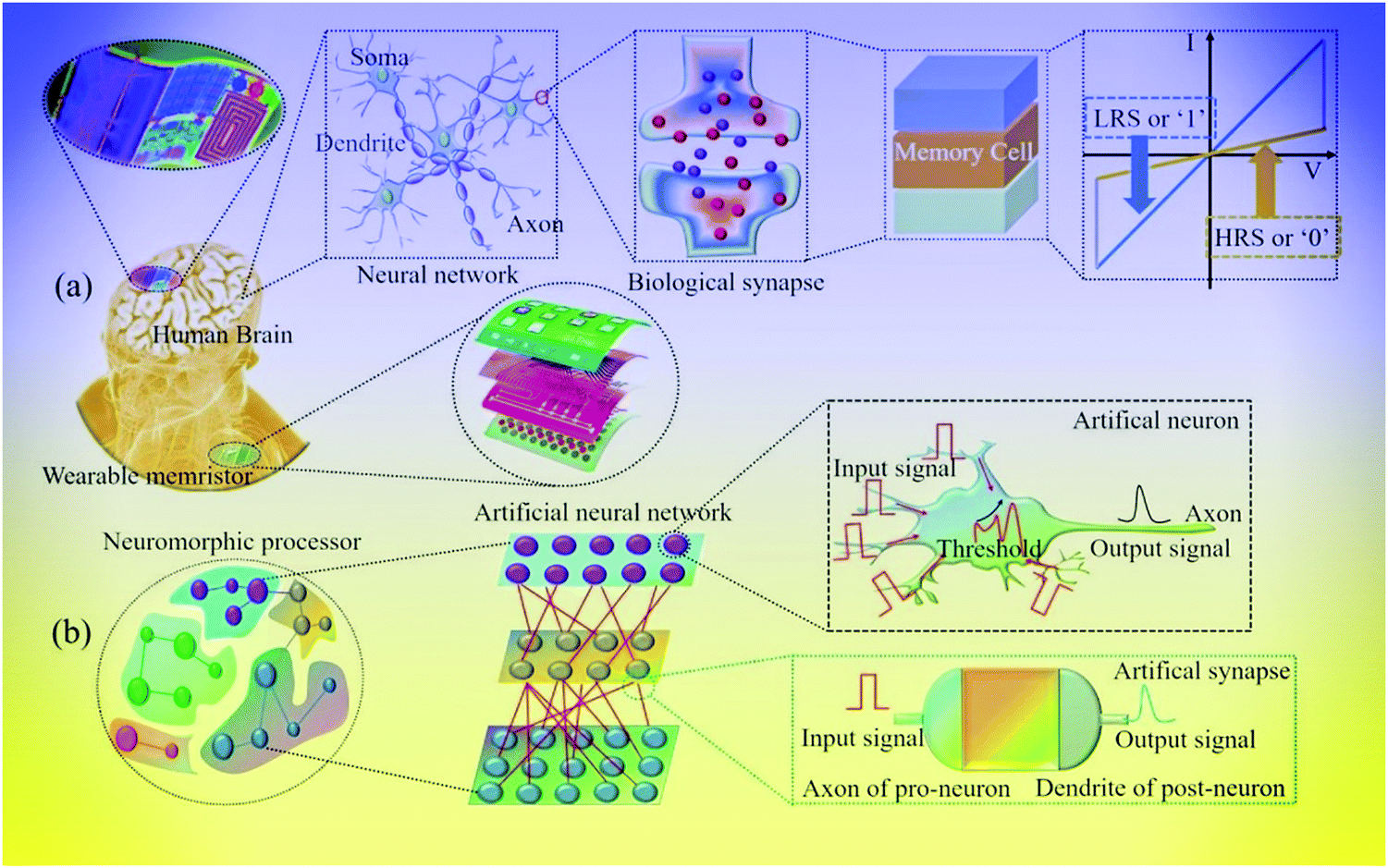 | ||
| Fig. 1 Main applications of memristors in information storage, artificial neural networks and neuromorphic computing. | ||
1.2 Biomaterial-based memristors
After more than ten years of development, many materials exhibit resistive switching behaviors when stimulated by electrical signals. The active materials of memristor devices can be divided into inorganic materials, organic materials and organic–inorganic materials as shown in Fig. 2. Organic materials mainly include natural biomaterials (lignin,28 egg,31 leaf32etc.) and polymer materials (glucose,33 polydopamine,34 PEI35etc.). Inorganic materials mainly include metal oxides (TiO2,36 HfO2,37 ZnO,38etc.), low dimensional materials (PbS quantum dots,39 Ag@AgOx nanowires,40 graphene oxidized,41etc.) and others (CsPbClxBr3−x,42 C3N4,43 TiOxFy,44etc.). In recent years, some organic–inorganic material heterojunctions (polymethylmethacrylate/Cs3Cu2I,45 poly{2,2-(2,5-bis(2-octyldodecyl)-3,6-dioxo-2,3,5,6-tetrahydropyrrolo[3,4-c]pyrrole-1,4-diyl)-dithieno[3,2-b]thiophene-5,5-diyl-alt-thiophen-2,5-diyl}/ZnO,46 TiO2/Cs0.05(FAxMA1−x)0.95PbBryI3−y,47etc.) have also been used as active layer materials to preparing memristor devices. Among these materials, due to the excessive consumption of some inorganic materials, it is urgent to find some environmental-friendly, sustainable and non-polluting biomaterials to replace them. Therefore, organic biomaterials have attracted researchers' interest due to their advantages, such as light weight, flexibility, ease of processing, and being pollution-free and recyclable.47–52 In fact, the research on the memory effect of organic materials can be traced back to the 1970s. At that time, Segui et al. prepared organic polystyrene films by a glow-discharge technique, and it showed reproducible bi-stable resistive switching behavior.53 Subsequently, the resistive switching memory behavior was observed in copper-tetracyanoquinodimethane polycrystalline films.54 From then on, great progress has been made by organic materials in the resistive switching memory behavior. Recently, organic polymeric materials and natural biomaterials inheriting the advantages of each material component become promising again to develop memristors with high performance.35,55–59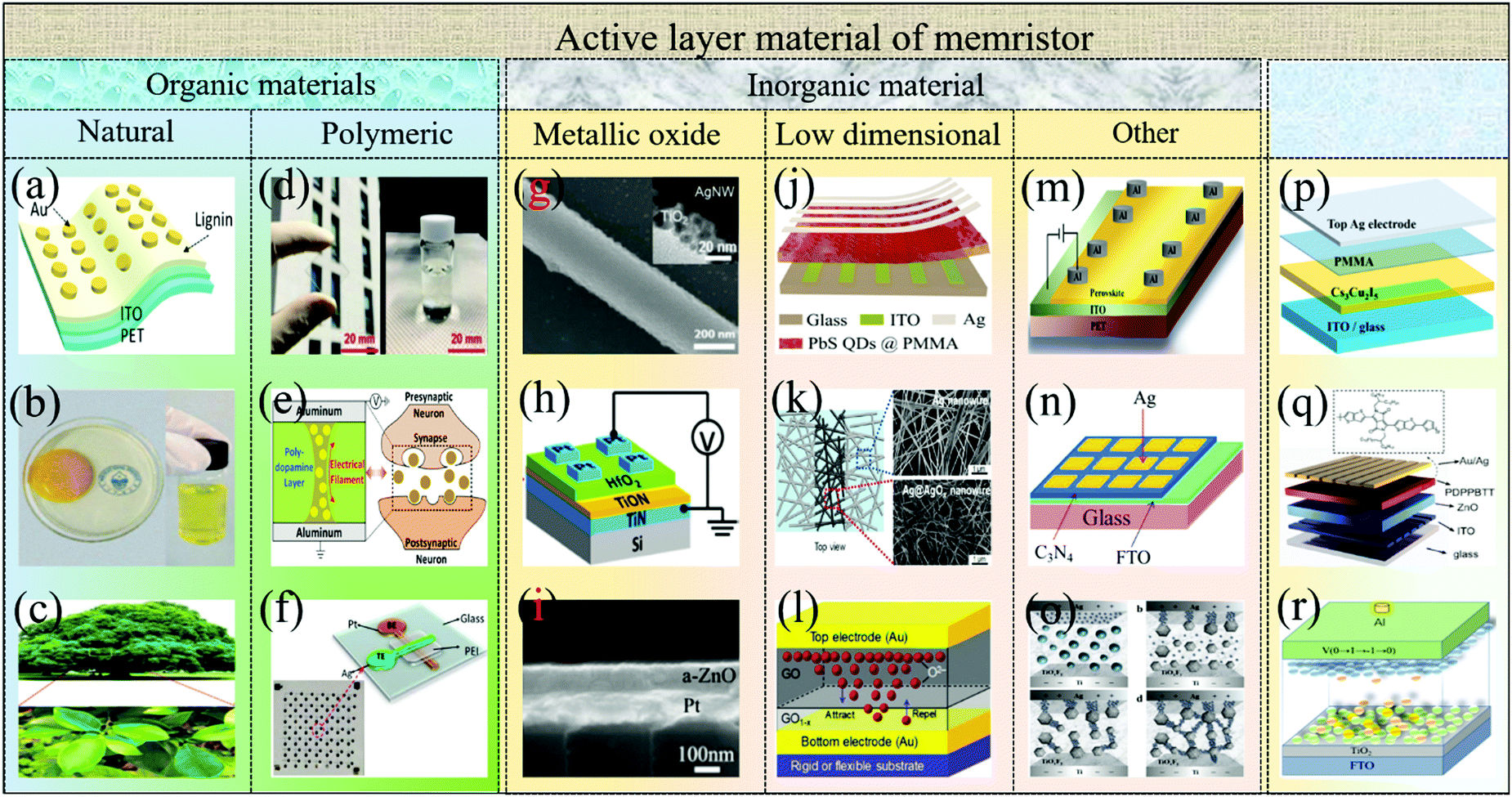 | ||
| Fig. 2 Memristor active layer material classification. (a) Lignin. Panel a reproduced with permission.28 Copyright 2017, American Chemical Society. (b) Egg. Panel b reproduced with permission.31 Copyright 2017, Royal Society of Chemistry. (c) Leaf. Panel c reproduced with permission.32 Copyright 2017, Elsevier. (d) Glucose. Panel d reproduced with permission.33 Copyright 2018, Wiley-VCH. (e) Polydopamine. Panel e reproduced with permission.34 Copyright 2019, Wiley-VCH. (f) PEI. Panel f reproduced with permission.35 Copyright 2019, Wiley-VCH. (g) TiO2. Panel g reproduced with permission.36 Copyright 2020, Elsevier. (h) HfO2. Panel h reproduced with permission.37 Copyright 2019, Royal Society of Chemistry. (i) ZnO. Panel i reproduced with permission.38 Copyright 2016, Royal Society of Chemistry. (j) PbS quantum dots. Panel j reproduced with permission.39 Copyright 2020, Royal Society of Chemistry. (k) Ag@AgOx nanowires. Panel k reproduced with permission.40 Copyright 2017, American Chemical Society. (l) Graphene oxidized. Panel l reproduced with permission.41 Copyright 2020, Royal Society of Chemistry. (m) CsPbClxBr3−x. Panel m reproduced with permission.42 Copyright 2017, American Chemical Society. (n) C3N4. Panel n reproduced with permission.43 Copyright 2018, Elsevier. (o) TiOxFy. Panel o reproduced with permission.44 Copyright 2016, American Chemical Society. (p) polymethylmethacrylate/Cs3Cu2I. Panel p reproduced with permission.45 Copyright 2020, American Chemical Society. (q) poly{2,2-(2,5-bis(2-octyldodecyl)-3,6-dioxo-2,3,5,6-tetrahydropyrrolo[3,4-c]pyrrole-1,4-diyl)-dithieno[3,2-b]thiophene-5,5-diyl-alt-thiophen-2,5-diyl}/ZnO. Panel q reproduced with permission.46 Copyright 2020, Elsevier. (r) TiO2/Cs0.05(FAxMA1−x)0.95PbBryI3−y. Panel R reproduced with permission.47 Copyright 2021, Elsevier. | ||
In recent years, many biomaterials have shown fascinating promise in the field of memristors.60–64 Most of these materials can be extracted from plants or animals by simple manipulation.65–73 Among them, some wastes, such as dead leaves, banana peels, orange peels, eggshells, etc., can be reasonably reused, which can alleviate current environmental problems. Therefore, multifunctional electronic devices with high-performance derived from biomaterials deserve more attention. When discarded, these electronic devices can degrade naturally without causing any pollution to the environment. Biomaterials as active layer materials of memristor devices can sustain the long-term development of memristor devices because they are renewable. The preparation of memristor devices using biomaterials not only enriches the candidate materials of electronic devices, but also expands the application prospect of memristor devices. In recent years, great progress has been made in the preparation of memristor devices based on biomaterials. Biomaterials are also ideal substrates for the fabrication of wearable devices because of their generally good ductility, transparency, and biocompatibility.
1.3 Applications of biomemristors
Flexible and transparent biomemristors are beneficial for implantable and wearable devices.74–78 Currently, biomemristors show fascinating application prospects in some scenarios, e.g. information storage,79–81 artificial electronic synapses,82 neural networks,83 and neuromorphic computing.61,62 In particular, there are many studies on the application of biomemristors to simulate the properties of artificial electronic synapses.82 For synapses, their plasticity reflects changes in the activity of neuronal connection strengths, and the synaptic plasticity is considered an important component of memory and learning.84 The resistance states of biomemristors can be modulated to increasing or decreasing, which is similar to bio-synaptic plasticity. Yan et al. prepared porous silk fibroin from bovine serum albumin and used it as the dielectric layer of biomemristors.82 They used the porous silk protein-based biomemristor device to simulate the excitation, inhibition, learning and memory behavior of synapses. This work provides a solution for developing biomemristors with simulated synaptic behavior.With the rapid development of science and technology, wearable and implantable electronic devices can be employed for health monitoring, disease diagnosis and treatment in future, as shown in Fig. 3. In 2019, Han et al. designed an artificial haptic neuron system by integration with a piezoresistive sensor and memristor.85 In this work, a piezoresistive sensor as a receptor converted mechanical signals into electrical signals, and a memristor as a synapse realized information transmission and processing. The device shows good durability (>7000 cycles) and high sensitivity, which are important factors for wearable applications. Therefore, some basic properties of wearable biomemristor devices and material characteristics are discussed in this section. Firstly, mechanical flexibility and biocompatibility are necessary for wearable biomemristive systems and potential applications. Second, it still needs to have relatively stable memory behavior under extreme conditions of bending or pulling up compared to the flat conditions. In the development of wearable biomemristor devices, some factors, such as printability, transparency, compatibility with various substrates, and mass production of biomaterials, must be considered. Raeis-Hosseini et al. designed and fabricated a flexible biomemristor whose resistive state did not degrade after 1000 cycles.86 In this work, data retention, durability, mechanical flexibility, and uniformity of wearable biomemristor-based memory devices have been demonstrated. Lee et al. fabricated a fully flexible high-density biomemristor using silk protein as the device dielectric layer on a 10 μm-thick Parylene-C substrate.65 The resistance values of the memristor devices at the HRS and LRS are almost indistinguishable in the flat and rolled states. In short, for wearable biomemristor devices, relatively reliable performance in any bending state is required. This outstanding flexibility and reliability have laid the groundwork for the commercialization of biomemristive devices.
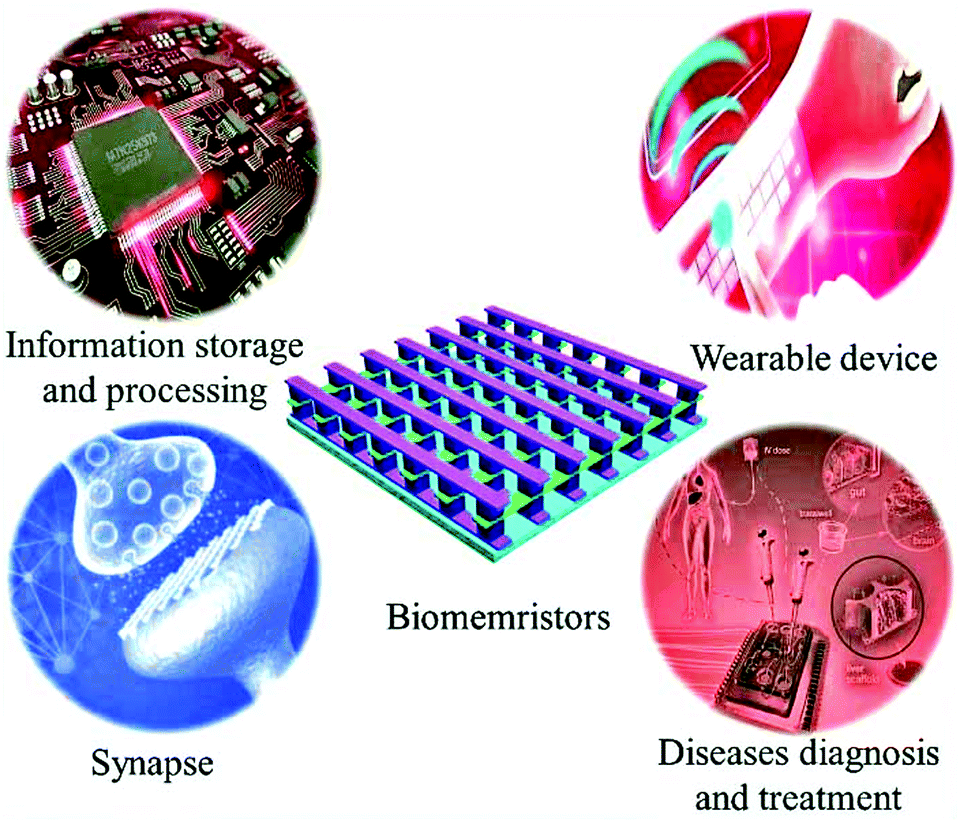 | ||
| Fig. 3 Application prospects of biomemristors. | ||
The illustration of a bio-perception system is presented in Fig. 4a. The artificial sensory nerve was constructed by using a piezoresistive sensor connected with a memristor as in Fig. 4a. This artificial sensory nervous system is expected to be used in biomimetic sensing systems and prosthetics. This work demonstrates that the piezoresistive pressure sensor connected to a memristor-fabricated artificial tactile neuron system has excellent durability and flexible sensitivity. The artificial sensory system materials and fabrication processes may be conducive to brain-machine interfaces. The human skin nervous system provides various protective and sensitive functions.87 When an external stimulus signal acts on the skin, the corresponding mechanoreceptors encode the signal as an ion transport-induced action potential. The induced action potential will be transmitted to the synapse through the nerve fibers as in Fig. 4b. Therefore, the electronic skin technology is a frontier research for the development of wearable electronic devices.
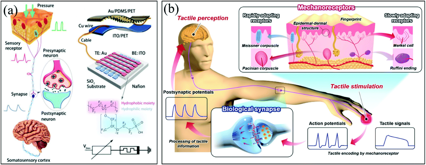 | ||
| Fig. 4 (a) Bio-haptic perception system and its composition. Panel a reproduced with permission.85 Copyright 2019, Wiley-VCH. (b) Schematic diagram of the human tactile perception system. Panel b reproduced with permission.87 Copyright 2020, Wiley-VCH. | ||
Although the application performance of the currently reported biomemristors still needs to be further improved, it is expected to achieve greater applications and play an important role in the era of artificial intelligence. With the development of biomemristors, many advantages will be revealed compared with that of other nonvolatile memory devices. Most importantly, the successful production of biomemristors provides a new route to material sources of electronic devices, as biomaterials are renewable and naturally abundant.21,88–94 In addition, some biomemristors are self-degradable in aqueous environments, which makes them attractive for personal privacy information protection and military applications.21,88 Moreover, these biomaterials are compatible with organisms. Thus, biomemristor devices based on biomaterials can be implanted into a living body for disease diagnosis and treatment without any other potential side-effects. Of course, the extreme flexibility of biomemristors makes them attractive in wearable electronic systems, which is difficult with inorganic materials. With the development of information technology, the wearable electronic systems will become an indispensable part of our daily life. The characteristics of flexibility, lightness, non-toxicity, and environmental protection are the basic requirements of wearable electronic devices. A wearable system automatically identifies the user's behavior, activity state and surrounding activity, and adjusts the functions or parameters of the system through these states. Therefore, we mainly discuss the research progress, working mechanism, potential applications, challenges and insights of biomemristors in this review.
2. Research progress
Natural biomaterials have attracted extensive attention in the field of wearable memristors due to their environmental friendliness, excellent mechanical properties, easy processing, biocompatibility, and degradability.89,95–97 Kundu et al. used silk fibroin to fabricate a biomemristor that exhibited a highly nonlinear dynamic response behavior in 2012.98 Since then, many studies based on biomemristors have been reported, and they have shown some attractive application prospects in bio-synapses and information storage. The development of biomemristors based on typical biomaterials is shown in Fig. 5, which provides a timeline for the development of biomemristors based on various biomaterials. In addition, this section also discusses the fabrication process, performance, and potential applications of biomemristors based on biomaterials, which contributes to a comprehensive understanding of biomemristors in terms of materials, structures, mechanisms, and properties.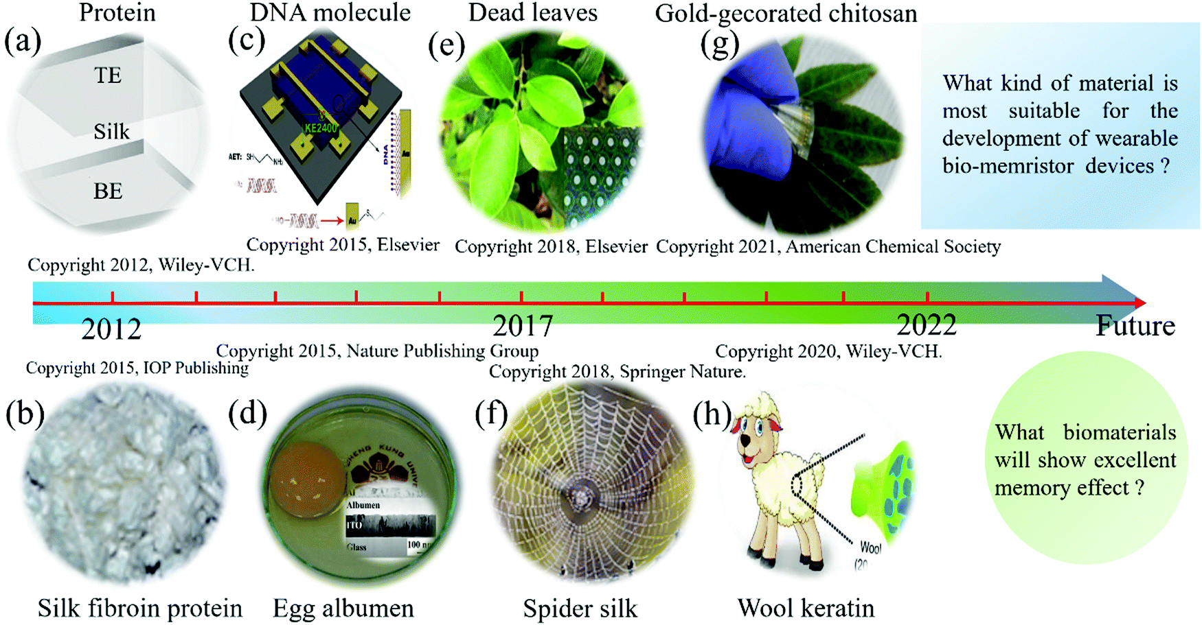 | ||
| Fig. 5 Brief schedule of the development of the biomemristor based on typical biomaterials. (a) Silk. Panel a reproduced with permission.98 Copyright 2012, Wiley-VCH. (b) Silk fibroin. Panel b reproduced with permission.90 Copyright 2013, Wiley-VCH. (c) DNA. Panel c reproduced with permission.79 Copyright 2015, Elsevier. (d) Egg albumen. Panel d reproduced with permission.91 Copyright 2015, Nature Publishing Group. (e) Dead leaves. Panel e reproduced with permission.32 Copyright 2017, Elsevier. (f) Spider silk. Panel f reproduced with permission.92 Copyright 2018, Springer Nature. (g) Gold-decorated chitosan. Panel g reproduced with permission.86 American Chemical Society. (h) Wool keratin. Panel h reproduced with permission.115 Copyright 2020, Wiley-VCH. | ||
2.1 Protein-based biomemristors
In all typical biomaterials, proteins, which are the building blocks of tissues, are important nutrients for the human body.93 Proteins possess many excellent properties, such as biocompatibility, electrical insulation, controllable mechanical properties, and biodegradability, and show attractive application prospects in the development of flexible and wearable electronics.65,86,99 In recent years, proteins have been extensively studied for their unique properties in the field of memristors. Herein, we will discuss the performance and potential applications of protein-based memristors.Silk protein has attracted extensive attention as a raw material for electronic devices due to its unique advantages such as photoelectricity, degradability, and mechanical strength.98–102 Initially, Kundu et al. fabricated a highly flexible and transparent biomemristor from silk cocoon silk protein, which exhibited a highly nonlinear dynamic response.98 Silk protein was used as the active layer of biomemristive devices, exhibiting resistive switching behavior under the stimulation of an electric field. The resistive switching mechanism of the device involves the formation and breaking of conductive filaments, while the switching of filaments between oxidized and reduced states also plays an important role. This work demonstrates the great potential application of the biomaterial silk protein in resistive switching memory. The silk fibroin from silkworm cocoons opens up new prospects for the next generation of novel concepts of memory. Then, by analyzing the resistance switching behavior in detail, they found that the conduction mechanism of silk fibroin was controlled by multiple charge transport, and pointed out that the amide I region is the main reason for the changes in silk fibroin conductivity at appropriate bias voltages.90
Different from the atomic functionalization of solid materials, mesoscopic functionalization involves incorporating mesoscopic dopants, namely functional molecules or nano materials or quantum dots, into the mesoscopic network of soft materials to give the material special properties without damaging its original properties. In 2017, Liu et al. fabricated electronic devices using wool keratin molecules incorporating gold nanoclusters as mediator molecules into the silk fibroin mesoscopic network.103 In this work, the wool keratin with gold-nanocluster @silk-fibroin (AuNC@SF) was used as an active layer to fabricate the memristive devices. The wool keratin with gold nanoclusters is rich in electrons, which can act as electronic charges to bridge the growth of conductive channels in biodegradable memristors. Fig. 6a demonstrates the WK@AuNC complexes on the SF material thin film with a size of about 70 nm. Fig. 6b shows the micrograph of the Ag top electrode with a diameter of about 90 μm. The structural schematic diagram and I–V behavior curve test circuit diagram of the biomemristor are shown in Fig. 6c. The role of gold nanoclusters in the mesoscopic network of silk fibroin was studied by comparing memristors fabricated without and with gold nanocluster-doped silk fibroin under the same conditions, and the corresponding performance is shown in Fig. 6d–i, respectively. In Fig. 6d, the process of switching the device from the HRS to the LRS is called set. Conversely, the process of switching the resistance state from the LRS to the HRS is called reset. It can be found that gold nanoclusters embedded into the mesoscopic network of silk fibroin can improve the stability of memristor devices, e.g. endurance, and set and reset threshold voltage. Furthermore, the threshold voltage value of set and reset becomes smaller but the HRS/LRS ratio (∼100) becomes higher. This higher HRS/LRS ratio can avoid misreading memory operation. The resistance switching behavior was studied by cycle sweep voltage, and the I–V behavior curve is shown in Fig. 6j. Initially, the set-stop voltage is continuously set (increased) and the resistance of the device gradually decreases from the HRS to the LRS. The absolute value of the set (boost) and reset (drop) voltages increases as the scan sequence voltage range increases. This means that biomemristors can act as synaptic devices, a modulation property that has never been reported in pure silk-prepared devices. This type of I–V curve with analog signals can express changes of synaptic weights by potentiating or depressing stimulation. In Fig. 6k, this gradual conductance tuning behavior of biomemristors was investigated by applying a pulse stimulation mode. It can be found that the conductance increases with the increase of the positive pulse sequence. In contrast, it shows the opposite characteristics under a negative pulse. The synapse weight change of spike-timing-dependent plasticity (STDP) was tested and is fitted in Fig. 6l. The resistive switching behavior of this biomemristor was explained by the formation and fracture of conductive filaments. This work showed that mesoscopic functionalization can not only greatly improve the electrochemistry properties of materials, but also endow them with new functions. Compared with pure SF-based devices, it possesses unique synaptic properties and synaptic learning ability, which are of great significance for non-volatile memory devices. The mesoscopic functionalization will endow SF materials with specific functions, which provides a promising prospect for the preparation of wearable electronic devices with biocompatibility and controllable biodegradability.
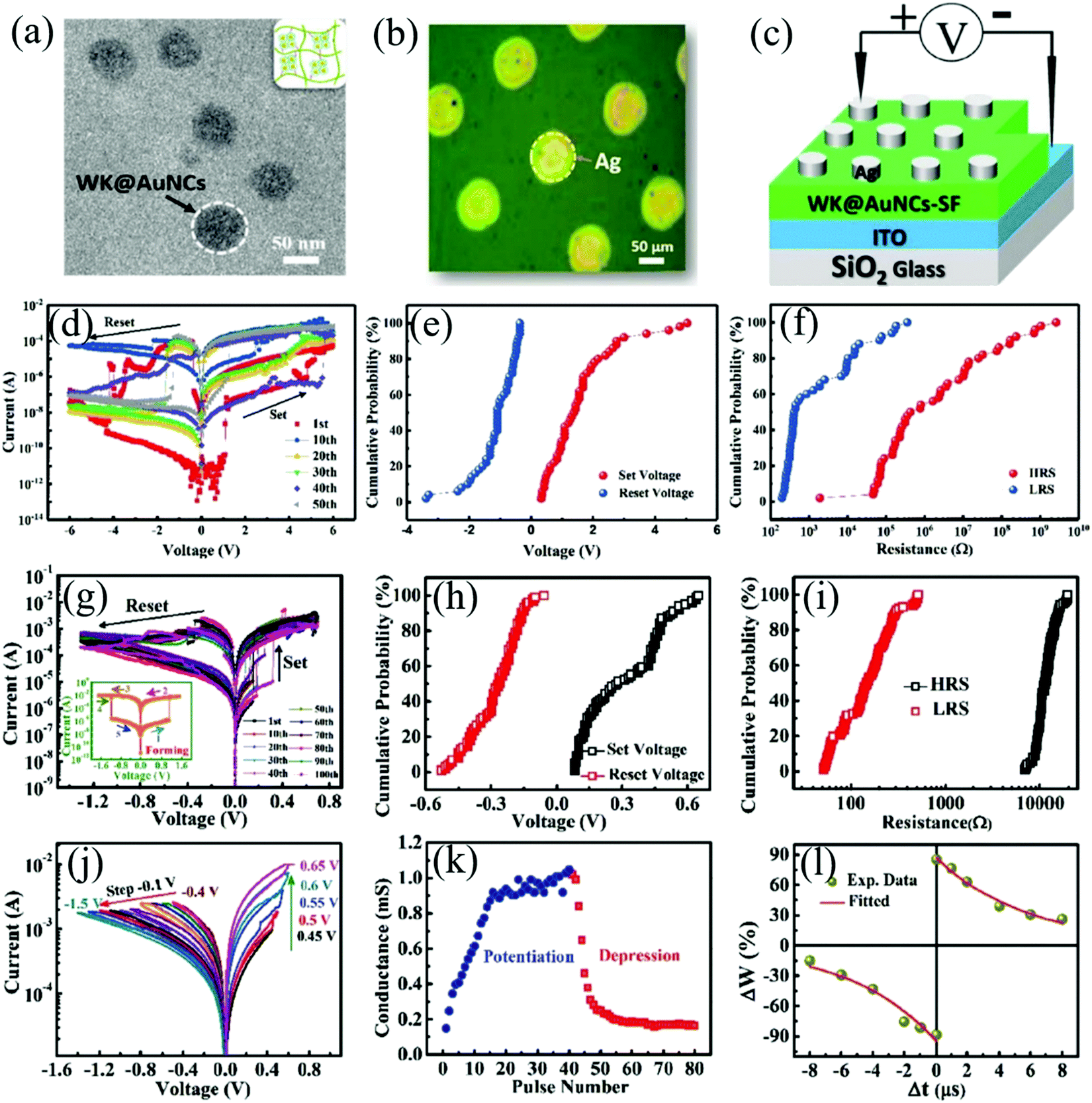 | ||
| Fig. 6 (a) TEM image of SF materials WK@AuNCs. (b) The biomemristor device top electrode Ag microscope photograph. (c) Device structure and I–V curve test circuit diagram. (d–f) Neat-SF fabricated device I–V curves, set and reset voltage distribution, HRS and LRS distribution, respectively. (g–i) The Ag/WK@AuNCs@SF/ITO device I–V curves, set and reset voltage distribution, HRS and LRS distribution, respectively. (j) The device continuous modulation I–V curve. (k) The device potentiation and depression properties in the pulse stimulation mode. (l) The device spike-timing-dependent plasticity behavior. Panels (a–l) reproduced with permission.103 Copyright 2017, Wiley-VCH. | ||
Metal ions in proteins play important roles in charge transfer and storage.104 Ferritin also belongs to a kind of silk protein which has distinctive properties.105 In 2014, Chen et al. fabricated a memristor with stable and tunable properties by assembling ferritin within the ∼12 nm gap created by in-line lithography.105 The ferritin-based memristor fabricated by a bioengineering process is shown in Fig. 7a. Firstly, FeSO4 solution was added in 0.1% HCl, and it was incubated at room temperature for 1 h. Next, the mixture solution was incubated overnight at 4 °C. These unbound metal ions were removed using desalting technology, and the encapsulated metal quantity has been characterized using inductively coupled plasma spectrometry technology. Finally, these protein materials with various Fe loads were used as the dielectric layer of memristor devices. The accuracy of preparing nanogaps using chemical methods is higher than that when using physical methods, and using electrochemical deposition methods nanogaps down to 1 nm can be prepared.106,107Fig. 7b shows the I–V curves of biomemristor devices with ∼12 nm on-wire lithography-fabricated gaps before and after immobilization of recombinant Archaeoglobus fulgidus ferritin with 1200, 2400, 4800 and 7200 Fe loading, respectively, and the I–V curve suggests that protein loaded Fe atoms play an important role in the memory effect of the device. With the increase of Fe loading in proteins, the I–V behavior curve of a biomemristor device is more obvious, and its resistance ratio was gradually changed from 1 to 4 at an operating voltage of 0.6 V. In contrast, empty nanogap or 3-mercaptopropionic acid-modified nanogap devices exhibited no conductance within a certain noise limit, indicating that ferritin was successfully immobilized in the nanogap. Notably, the biomemristor achieved tunable resistance switching behavior by controlling loading Fe atom content in protein, and the ION/IOFF ratio and memory behavior are schematically shown in Fig. 7c. The resistive switching mechanism of this device is attributed to the higher redox activity of the inorganic Fe composite core at higher iron loadings. This work shows that bioengineering techniques can significantly achieve higher application functions of memristor devices. Furthermore, in 2016, Li et al. fabricated a biomemristor based on ferritin, and it shown excellent resistance switching behavior with a high HRS/LRS ratio (>105) and long term stability (>6 × 10³ s).108 The schematic diagram of ferritin and the I–V curve of the biomemristor at different compliance currents are shown in Fig. 7d, and the resistance switching behavior and threshold switching performance of the biomemristor were realized by setting different compliance currents. Normally, iron ions are stored in the core, and protein substances are wrapped around the iron ions to form a spherical shell. The iron ions in ferritin can be released from the spherical shell under the action of an electric field, which may lead to the resistive switching behavior.105 The memory switching behavior of the biomemristor with a Pt/ferritin/Pt/SiO2/Si structure and threshold switching can be controlled by adjusting the compliance current. Threshold switching was observed at a compliance current of 100 nA and direct current voltage sweeps (0 → 4 V → 0). In the 0 → 4 V sequence, the current suddenly increases to achieve the LRS at ∼1 V. This process is called the set process, and the corresponding voltage is called Vth. When the voltage sequence is 4 V → 0, the current suddenly decreases at ∼0.15 V, and the resistance state switches from the LRS to the HRS. This process is called the reset process, and the corresponding voltage is called Vhold. When the compliance current is 100 μA, this biomemristor device presents memory switching behavior. The performance of the biomemristor from threshold switching to memory switching is shown in Fig. 7e, which shows that threshold switching and memory switching are mutually converted by controlling the compliance current. Considering that Pt is an inert electrode, the Fe ions may be the source of conductive filaments in ferritin films. The low compliance current (<5 μA) may limit the growth of conductive filaments, and it further leads to the natural fracture of conductive filaments and the emergence of volatile switching.109,110 This biomemristor with both nonvolatile memory switching and volatile threshold switching properties makes it promising for novel logic function applications.
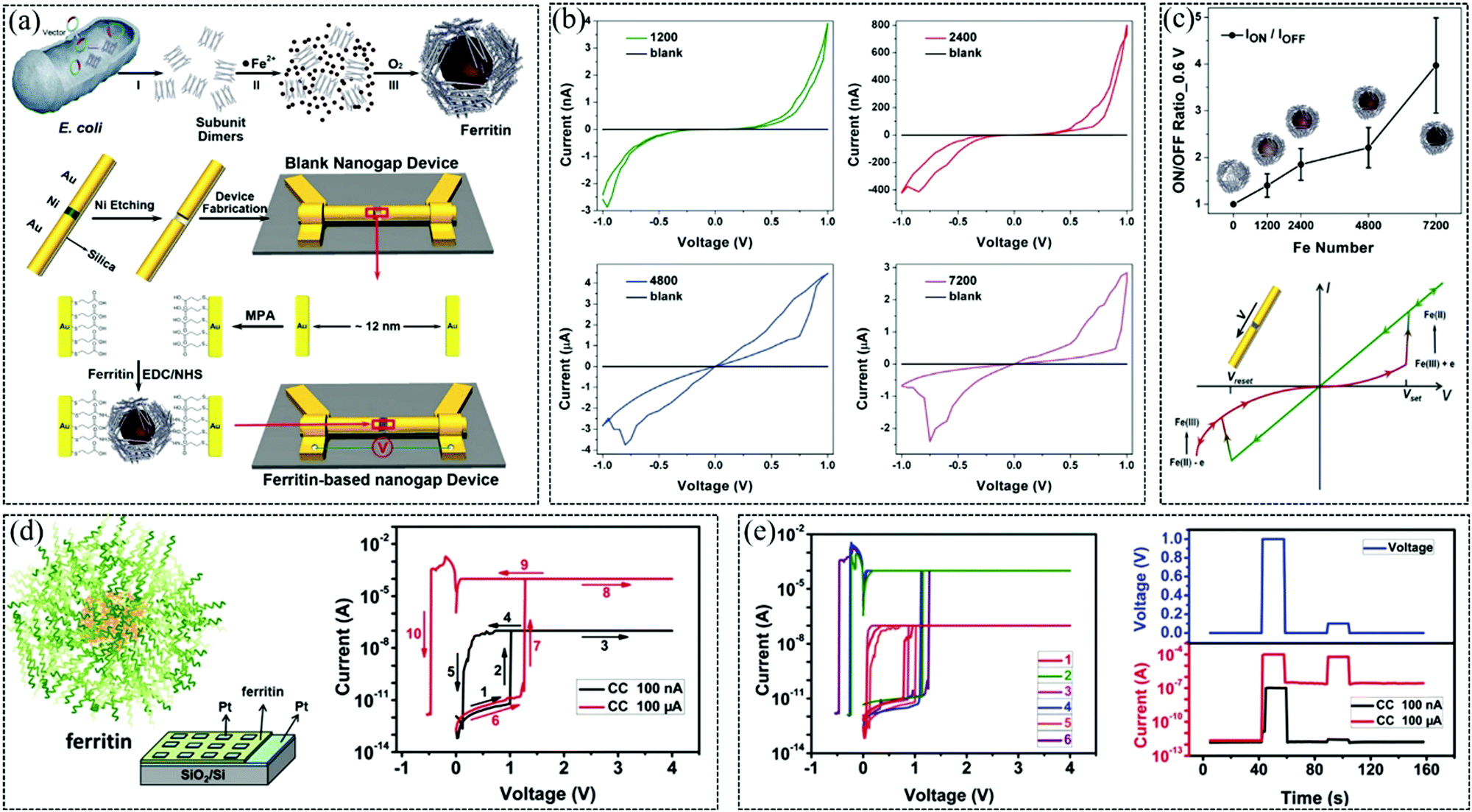 | ||
| Fig. 7 (a) Fabrication of a ferritin-based memristor using bioengineering. (b) I–V curves of ∼12 nm on-wire lithography-fabricated gaps before and after immobilization of recombinant Archaeoglobus fulgidus ferritin with 1200, 2400, 4800 and 7200 Fe loading. (c) The Ion/Ioff ratio of the memristor with different Fe loadings at 0.6 V and I–V curve. Panels (a–c) reproduced with permission.105 Copyright 2014, Wiley-VCH. (d) Schematic diagram of ferritin and the I–V curve of the biomemristor with different compliance currents. (e) Switching between volatile and nonvolatile and responding currents under a voltage pulse with 100 nA and 100 mA compliance current, respectively. Panels d and e reproduced with permission.108 Copyright 2016, Royal Society of Chemistry. | ||
Although previous studies have demonstrated the feasibility and potential advantages of protein materials in fabricating wearable biomemristors, still there is a need for further improvement before commercialization. The resistive switching of memristor devices between the HRS and LRS mainly depends on the formation and rupture of conductive channels between the two electrodes. To meet the requirements of sustainable wearable electronics, new approaches must be employed to comprehensively and accurately control the formation and rupture of conductive filaments embedded in biomaterials. In 2018, Lee et al. successfully prepared a nonvolatile biocompatible biomemristor device by drop-cast technology, and the device structure is Cu/recombinant molecular chaperone DnaJ (rDnaJ)/Pt/SiO2/Si.111 The as-prepared biomemristor shows ultra-low operation voltage (VSet ∼ 0.12 V, VReset ∼ −0.88 V), and the conductive bridges can be controlled by adjusting the protein protonation state. The storage and processing of real-time data information are an indispensable part of wearable electronic systems. This excellent memory behavior of biomemristor devices can be used to construct sequential logic circuits. Fig. 8a and b shows the schematic diagram of a sequential logic circuit (SR latch) and operation, which consisted of two memristor cells. The SR latch has two output signal states (Q and ![[Q with combining macron]](https://www.rsc.org/images/entities/i_char_0051_0304.gif) ), and they can be controlled and stored by input signals: S (set) and R (reset). The output signals of this device will maintain a previous value when both input signals S and R are low. When one input signal is high and the other is low, the Q is forced to be high or low, in which the Q remains fixed until the S or R changes. The above results show that the rDnaJ-6 biomemristor can be used to build logic sequential circuits, and it also suggested that the device can build the basic modules for future electronic devices. Fig. 8c shows that the biomemristor device has multilevel resistance state characteristics by setting different compliance currents. When the compliance current is changed, the VSet and VReset values almost maintained a constant but the current of the LRS was increased from 1 to 60 μA. In addition, the resistance state can be completely returned from the LRS to the HRS by the reset process. For wearability, a flexible polyethylene terephthalate (PET) substrate was used in the fabrication of this electronic device. In Fig. 8d, the mechanical stability of biomemristors based on PET substrates was investigated by resistance values of the LRS and HRS as a function of bending radius. Fig. 8d demonstrates that the resistance of the biomemristor has a high HRS/LRS ratio (∼106) at different bending radii and does not change significantly, indicating the excellent flexibility of the biomemristor. Therefore, this highly flexible biomemristor device is well suited for wearable electronics.
), and they can be controlled and stored by input signals: S (set) and R (reset). The output signals of this device will maintain a previous value when both input signals S and R are low. When one input signal is high and the other is low, the Q is forced to be high or low, in which the Q remains fixed until the S or R changes. The above results show that the rDnaJ-6 biomemristor can be used to build logic sequential circuits, and it also suggested that the device can build the basic modules for future electronic devices. Fig. 8c shows that the biomemristor device has multilevel resistance state characteristics by setting different compliance currents. When the compliance current is changed, the VSet and VReset values almost maintained a constant but the current of the LRS was increased from 1 to 60 μA. In addition, the resistance state can be completely returned from the LRS to the HRS by the reset process. For wearability, a flexible polyethylene terephthalate (PET) substrate was used in the fabrication of this electronic device. In Fig. 8d, the mechanical stability of biomemristors based on PET substrates was investigated by resistance values of the LRS and HRS as a function of bending radius. Fig. 8d demonstrates that the resistance of the biomemristor has a high HRS/LRS ratio (∼106) at different bending radii and does not change significantly, indicating the excellent flexibility of the biomemristor. Therefore, this highly flexible biomemristor device is well suited for wearable electronics.
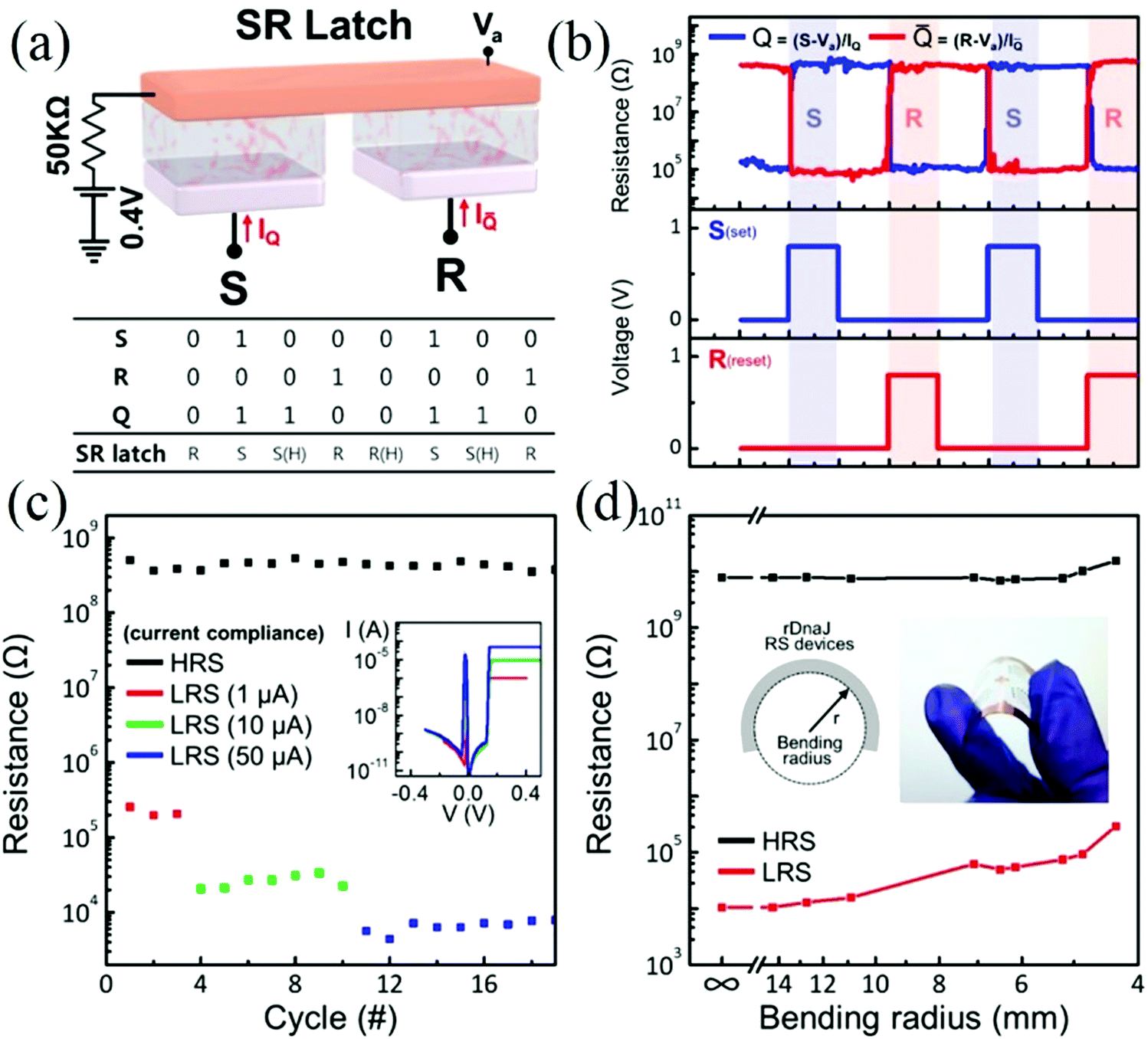 | ||
| Fig. 8 (a) The schematic diagram of the SR latch. (b) The operating result. (c) Multilevel LRS by set different compliance currents. (d) The resistance value at different bending radii. Panels (a–d) reproduced with permission.111 Copyright 2017, American Chemical Society. | ||
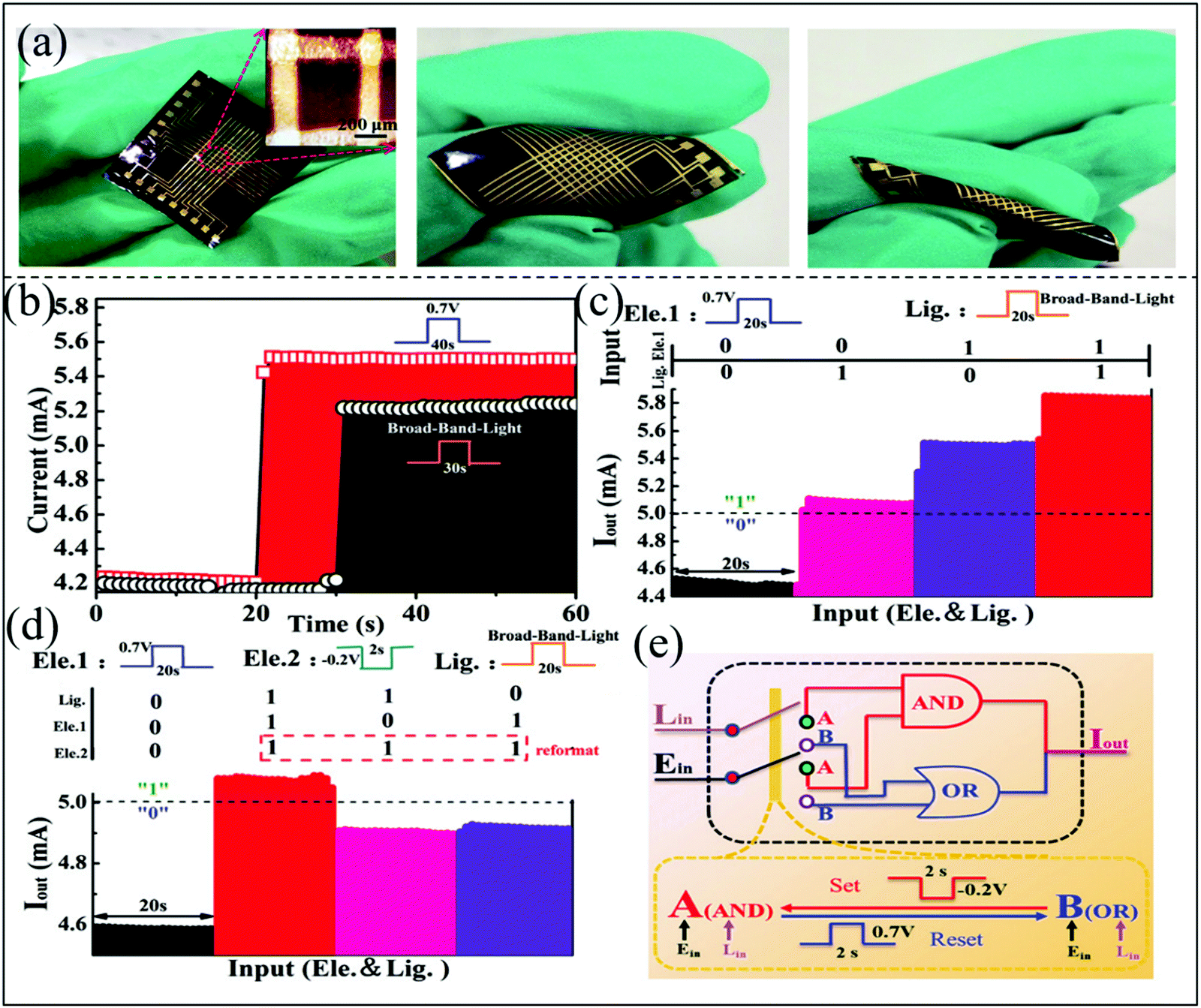
Egg albumen contains about 40 different proteins and minerals excluding water, especially the native egg albumen is trap-site rich.99,112 In 2019, Song et al. fabricated a wearable biomemristor using the albumen protein as the active layer of the device by a simple thermal and chemical reaction method, and it can realize the function of logical calculation.112Fig. 9a shows the optical images of a biomemristor at different bending radii, which reveal that the device has excellent flexibility and endurance. The albumen protein based biomemristors are highly depended on bias voltage and optical signals, which can be used as two independent input signals to the memristor to control the output resistance state. Fig. 9b–e shows the biomemristor can complete the memory logic function containing NOT, OR and AND gates at an applied voltage and light signal. An electrical signal of 0.7 V with 40 s or 30 s broad-band light signal was applied to the biomemristor in the LRS, a stable output current (>5.0 mA, defined as logic state ‘1’) was presented at a reading voltage of 0.2 V. Otherwise, it was defined as logic state ‘0’ for output current less than 5.0 mA. When one or both input signals were applied to the device, the output current was less than 5 mA, which was defined as the initial logic function ‘NOT’. However, when one or both input electrical signals were applied to the device for 20 s, the output current (5.0 → 5.8 mA) signals were higher than 5 mA. The logical state of ‘1’ was obtained, and this process corresponds to logical function ‘OR’ in Fig. 9c. This electrical reformatting process can be used as the ‘AND’ operation to erase the input and output signals, which is very important to release the device subsequent workload.113 Therefore, when an additional electrical signal (−0.2 V/2 s) was added, the final output signal depends on three input signals. When 0.7 V/40 s electrical and 30 s broad-band light signals were simultaneously applied on the device, the logical state ‘1’ was obtained. Otherwise, the output current (4.6 → 4.9 mA) was less than 5 mA, which corresponds to logic state ‘0’. This process corresponds to the ‘AND’ gate in Fig. 9d. A schematic diagram of the operation principle of such a typical storage logic unit is shown in Fig. 9e. The resistance switching behavior of the biomemristor shows serious fade when it was inserted in solution with different pH values for 10 min, but the crossbar structure of the biomemristor device was still maintained. This result suggests that the biomemristor based on albumen protein is promising for wearable applications in extreme working environments. In this work, the researcher has not tested the remaining beam structure memory behavior of the biomemristor after solution treatment. However, this work aims to show that the egg albumen substrate and memristor array structure have good durability under acid–base conditions, which provides good guidance for the development of biomemristors in extreme environments.
 | ||
| Fig. 9 (a) The photographs of the biomemristor with a Au/albumen/Au structure under different bending states. (b) Two different input signals: light and electric. (c) Output current signal under the action of light and electric signals. (d) Output current signal under the action of one light and two electric signals. (e) The schematic diagram of logic gate switching. Panels (a–e) reproduced with permission.112 Copyright 2019, Royal Society of Chemistry. | ||
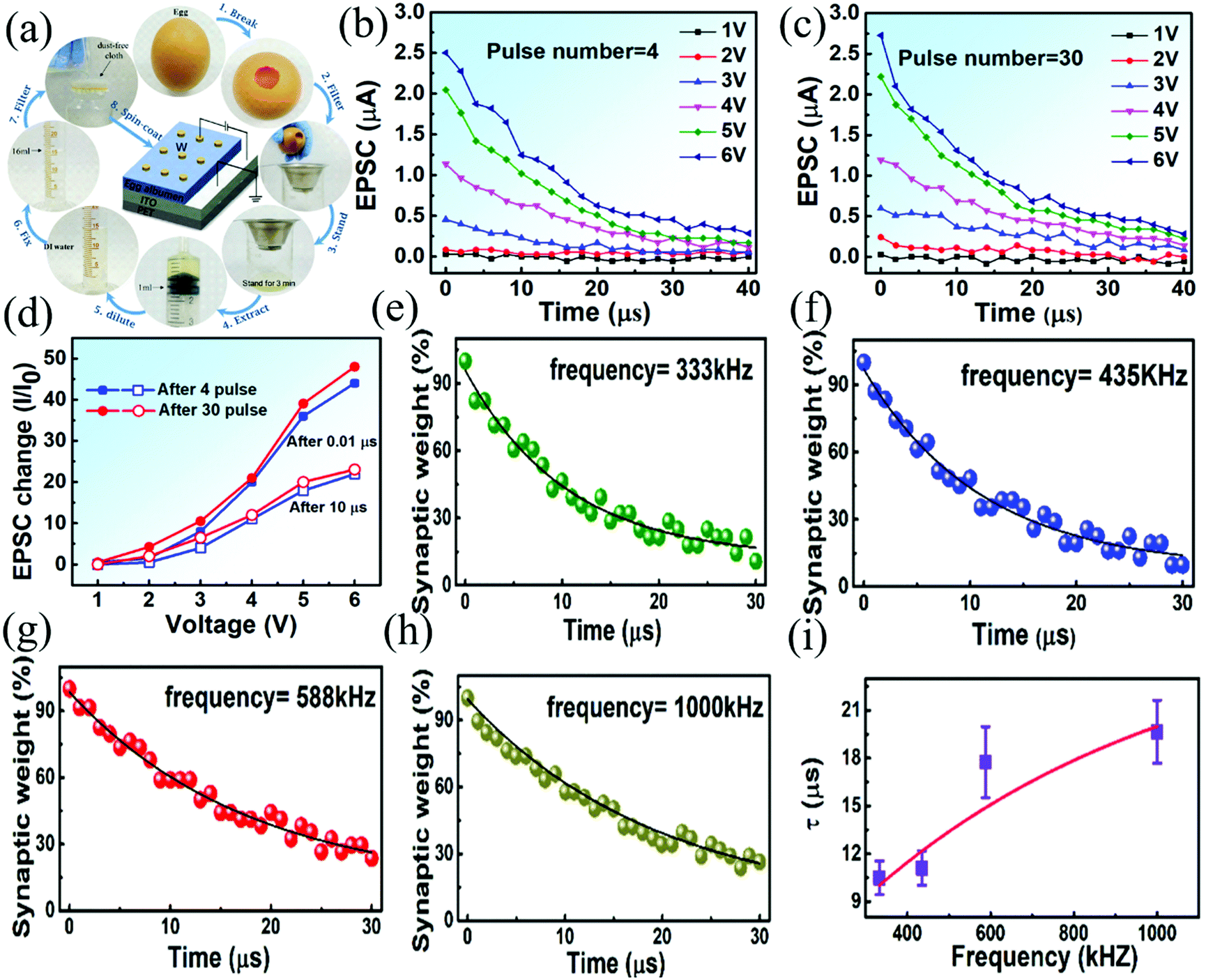
In the same year, a flexible and highly transparent biomemristor with a W/egg albumen/ITO structure on the PET substrate was fabricated by Yan et al.52 This biomemristor device demonstrated resistive switching performance without significant degradation under mechanical action. The preparation process of the biomemristor based on egg albumen is presented in Fig. 10a. As we all know, both short-term plasticity (STP) and long-term plasticity (LTP) existed in the memory of the human brain, and STP can be transformed into LTP after certain training. This behavior can be achieved by short-term or long-term resistance modulation of memristor devices. In Fig. 10b and c, the excitatory postsynaptic current (EPSC) was measured by applying 4 and 30 consecutive positive voltage pulse signals with different amplitudes, respectively. The interval and width of a signal pulse were fixed at 2 μs, and the pulse amplitude range was 1 → 6 V. The EPSC change was calculated by comparing the initial current I0 and measured current after 0.01 and 10 μs. The relationship between the EPSC and voltage pulse signal amplitude is shown in Fig. 10d. According to the time duration of EPSC, it can be divided into STP and LTP behavior. STP behavior can be defined as EPSC which almost maintains the initial value at small pulse amplitudes, and LTP behavior is that EPSC enhancements can persist after 10 μs at larger pulse amplitudes, as shown in Fig. 10b. In addition to the pulse amplitude, the frequency of the pulses also affects the synaptic properties of the device. Therefore, the effect of voltage signal pulse frequency on the EPSC of the memristor was studied as in Fig. 10e–h. The amplitude and width of the pulse voltage were fixed at 5 V and 1 μs. The synaptic weight sharply decreased from the initial level, and then decreased gradually over time. The test data at different frequencies were fitted using the Kohlrausch equation, which presents a function of forgetting. The relaxation time (τ) increases with the increase of pulse frequency, which indicates that the current delay time of the memristor is longer, as shown in Fig. 10i. The EPSC attenuation can be caused by the diffusion of conductive filaments during these two pulses.114 The ion diffusion between two pulses can be filled by the next pulse, and then the rate of rupture and formation of conductive channels is influenced by the interval time. A chemical bond was formed (break) in the dielectric layer material of the biomemristor device, and it can absorb (release) the electrons and hydrogen atoms. The resistive switching was caused by the limited migration of metal ion and iron ion redox (Fe ⇌ Fe3+ + 3e−) in the dielectric layer of the device.61 This result shows that the synaptic functions of the biomemristor can be adjusted by applying voltage pulse signals with different amplitudes, and the biomemristor device can be completely degraded in deionized water. This work suggests that the albumen-based biomemristor device is biocompatible and biodegradable with synaptic characteristics.
 | ||
| Fig. 10 (a) The fabrication process of the biomemristor device with a W/egg albumen/ITO/PET structure. (b) The EPSC results under the action of 4 consecutive pulses. (c) The EPSC results under the action of 30 consecutive pulses. (d) Relationship between EPSC and pulse amplitudes. (e–h) The EPSC performance at different stimulation frequencies. (i) The relationship between relaxation time and pulse frequency. Panels (a–i) reproduced with permission.52 Copyright 2017, American Chemical Society. | ||
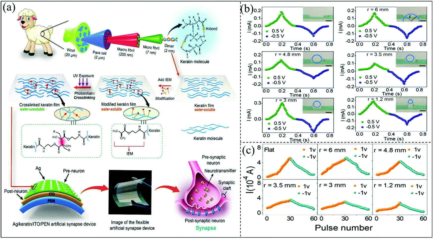
Exploring new memory functions by using suitable functional materials is crucial for the development of wearable biomemristors. In 2020, Liu et al. prepared a flexible and insoluble biomemristor device using chemical cross-linked wool keratin as the active layer.115 This biomemristor device is very promising in implantable and wearable systems. Wool keratin generally contains a random coil structure and an α-helical structure,116 and the structure that releases the filler peptides helps improve the flexibility.117 Wool keratin chemically cross-linked with large polypeptide chains is insoluble in water.118Fig. 11a shows the schematic illustration of the biomemristor based on cross-linked wool keratin, which can be used as an artificial synapse. The biomemristor was characterized for its maneuverability under different mechanical bending conditions. Fig. 11b shows the current–time (i–t) curves of biomemristors at different bending radii, and the corresponding synaptic potentiation/inhibition behaviors are also presented. It can be found that the device still functions perfectly even with a bending radius of 1.2 mm. This work demonstrates that biomemristor devices based on keratin resistance switching and synaptic behaviors are improved by chemical cross-linking processing techniques.
 | ||
| Fig. 11 (a) The flexible biomemristor with a Ag/wool keratin/ITO/PEN structure and the schematic illustration of the artificial synapse. (b) I–t curve with different flat radii. (c) The synaptic potentiation/depression at different flat radii. Panels (a–c) reproduced with permission.115 Copyright 2020, Wiley-VCH. | ||
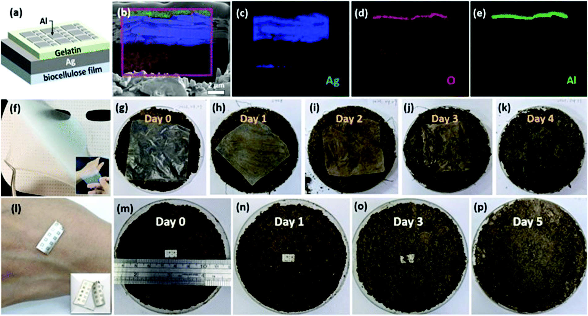
In 2021, Chang et al. prepared a flexible biomemristor by using biocellulose as the substrate and gelatin as the active layer, whose ductility made it adapt to different concave convex faces.119 This flexible characteristic made the biomemristor device have potential application in the field of wearable electronics. The biomemristor with a Al/gelatin/Ag/bio-cellulose structure shows a high HRS/LRS ratio (>104) and low operating voltage (<3 V), and the cross-sectional image of the biomemristor is shown in Fig. 12b. Moreover, the substrate material of the biomemristor can be naturally degraded in soil, and this biomemristor can also withstand the effects of human skin temperature and perspiration. Fig. 12 shows that cellulose films and biomemristor devices can be degraded. The degradability of the device was demonstrated by burying the device in a Petri dish with soil and the entire biocellulose membrane degraded completely within 5 days.120 This research work shows that the biomemristor device is a forward-looking development, which can be applied to the physiological evaluation and daily recording of wearable devices, providing opportunities in the biomedical field for future.
 | ||
| Fig. 12 (a) The biomemristor with a Al/gelatin/Ag structure. (b) The cross-sectional focused ion beam micrograph. (c–e) EDS chart analysis result of silver, oxygen, and aluminum, respectively. (f) Obtained biocellulose. (g–k) The degraded process photographs of biocellulose. (l) The photograph of the biomemristor stuck on the skin. (m–p) The degraded process photographs of the biomemristor. Panels (a–p) reproduced with permission.119 Copyright 2021, American Chemical Society. | ||
Natural biomaterials tussah hemolymph (TH) can be easily obtained from tussah organisms. In 2021, Wang et al. investigated the resistive switching memory behavior of the biomemristor using TH as the active layer.121Fig. 13a shows the structure diagram and optical picture of a biomemristor device with high transparency and flexibility. The TH as the dielectric layer of the biomemristor device was created on tin-doped indium oxide (ITO) by spin coating technology, and the electrodes were prepared by a thermal evaporation method. Such a flexible biomemristor device with a Al/TH/ITO/PET structure was prepared. Fig. 13b shows the output signal of the biomemristor device with two different input signals, respectively. When a voltage pulse (3 V/2 ms) was applied to the device, the output current was greater than 1 × 10⁻⁴ A, which was defined as logical ‘1’. Otherwise, it was defined as logical ‘0’. Thus, the output current is ∼1.66 × 10⁻⁶ A (‘0’) when a voltage pulse of 1 V/2 ms is applied to the device. The function of logic display can be realized because its output current has high stability. The ASCII code table was used for coding; ‘B’ can be coded as ‘01000010’. Like this, the first four letters of the word “biomemristor” are displayed through the logic display function of the device as in Fig. 13c. The resistance state of the device depends on the applied voltage amplitude. When the applied voltage exceeds the threshold voltage, it can be switched from the HRS to the LRS. A voltage (0.3, 1, 0.3, 3, 0.3 V) signal was applied when the biomemristor compliance current was 1 mA. The initial state of the device has not been changed and was still in the HRS at a read voltage of 0.1 V. Fig. 13d and e shows the input voltage and output response current signal of the biomemristor. Based on this characteristic, the current output depends on the voltage amplitude, and the “OR” and “AND” gates are shown in Fig. 13f and g. The logic working principle is present in Fig. 13h, in which the resistive switching behavior of the biomemristor device can be attributed to the formation and fracture of conductive filaments, oxygen ion migration, and the redox reaction of metal cations. Therefore, this biomemristor shows bipolar resistive switching behavior with a retention time of over 104 s in a bent state, which can be expected to be used in flexible wearable and green electronic devices.
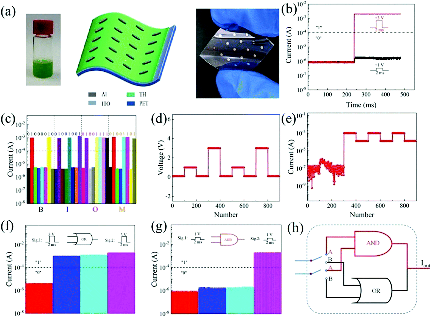 | ||
| Fig. 13 (a) The schematic diagram and optical picture of a flexible biomemristor device with a Al/TH/ITO/PET structure. (b) Two input voltage signals. (c) The word “BIOM” logic display by the memristor output current response under continuous pulse. (d) Input voltage. (e) Out current. (f and g) ‘OR’ and ‘AND’ gates. (h) Logic cell work principle. Panels (a–h) reproduced with permission.121 Copyright 2021, Molecular Diversity Preservation International. | ||
2.2 Polysaccharide-based biomemristors
Polysaccharides, e.g. chitosan and cellulose, are considered for use in transistors, and memristor, and synaptic devices.122–124 Recently, starch has been studied in electrochemical systems because of its many advantages, e.g. abundant sources and low-price.125 Potato starch has reasonable ionic conductivity because it contains two water molecules with tight and loose types in the microcrystalline network.126 In 2016, Lee et al. prepared a biomemristor using starch and starch–chitosan as active layers, respectively.127 The resistive switching behavior of the biomemristor can be regulated by mixing starch and chitosan in the dielectric layer of the device. This device based on starch showed digital resistive switching behavior. However, it showed analogous resistive switching behavior when starch and cellulose were mixed. The resistive switching behavior was explained by the formation and fracture of carbon-rich conductive filaments. The schematic illustration of a flexible biomemristor device is shown in Fig. 14a, and the I–V behavior was tested under bending and flat conditions. The I–V behavior curves under flat and bending (r = 5 mm) conditions are very similar, which shows that the memory properties of biomemristors with Au/starch/ITO/PET and Au/starch-chitosan/ITO/PET structures were quite stable under the tension and compression conditions, as shown in Fig. 14b–e. Therefore, the biomemristor with a starch-chitosan active layer shows a gradually changing set/reset characteristic, which can be expected to be used in wearable neuromorphic devices.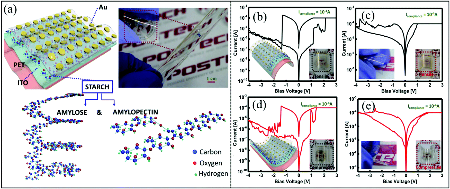 | ||
| Fig. 14 (a) The structural diagram and optical photograph of a flexible biomemristor device. (b and c) The I–V behaviors of Au/starch/ITO/PET and Au/starch–chitosan/ITO/PET biomemristor devices under tensile bending. (d and e) The I–V behaviors of Au/starch/ITO/PET and Au/starch–chitosan/ITO/PET biomemristor devices under compressive bending. Panels (a–e) reproduced with permission.127 Copyright 2020, American Chemical Society. | ||
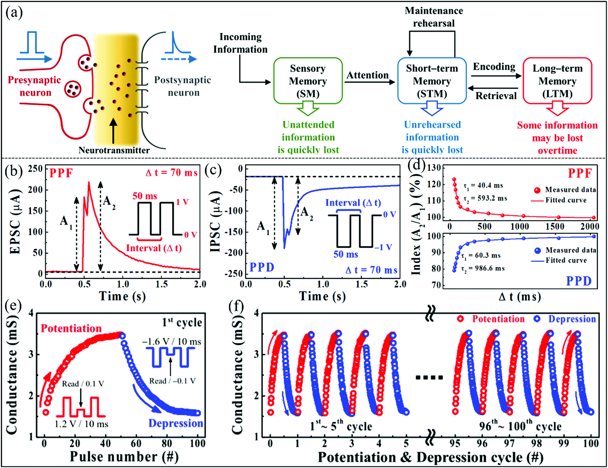
Despite the biomemristors having many potential advantages, their unstable multilevel resistance states and poor reliability must be overcome. Chitosan naturally exists in crustacean shells with abundance and biocompatibility, and it contains amines and hydroxyl groups which can easily react with metals.128 Chitosan can be used as a candidate material for optoelectronic devices due to its ability to form uniform and transparent films.62 In 2021, Cho et al. fabricated a biomemristor with a Ti/solid polymer electrolyte–chitosan/Pt structure, which showed excellent multilevel resistance switching behavior with good retention properties (>104 s).64 Furthermore, the artificial synaptic behavior can be implemented with an analogous switching effect of the device. Moreover, multilevel I–V behavior can be achieved by setting different compliance currents. Fig. 15a shows the schematic diagram of a biosynapse, learning and memory model, respectively. This learning and memory model was suggested by Atkinson and Shiffrin.129 According to this model, some unnoticed information is quickly lost in the brain, but the information that humans pay attention to is stored as short-term memory (STM). The STM will be switched to long-term memory (LTM) by maintenance rehearsal. Paired-pulse facilitation (PPF) is a characteristic phenomenon in bio-synapses. When two consecutive pulses are applied, the response amplitude of the second pulse will be larger than that of the first, and it depends on the time interval of the two pulses. The PPF and paired-pulse depression (PPD) behaviors are key characteristics for short-term synaptic plasticity, which are important for excitatory and inhibitory responses between adjacent synaptic connections. A larger excitatory postsynaptic current (EPSC) for PPF or a smaller inhibitory postsynaptic current (IPSC) for PPD can be triggered by a second postsynaptic pulse. Fig. 15b and c present EPSC and IPSC behavior appearing when using the paired presynaptic spikes under positive pulses and negative pulses, respectively. Fig. 15d summarizes the PPF and PPD responses as a function of time interval. When the time interval becomes short (60 ms), the PPF response index will be increased to ∼123%, and the PPD response index will be decreased to ∼79%. However, when the time interval becomes long (>2000 ms), both the response indices can be reduced to ∼100%, and the features can be used to simulate the bio-synapse function.130 The fitting results are very similar to the synapse performance, which can be divided into two stages of fast and slow for lasting time ranges from tens to hundreds milliseconds.131 To explore the switching performance of device analog filaments, the potentiation/depression conductance modulation behavior was characterized by presynaptic pulses. One and 100-cycle potentiation/depression behaviors are shown in Fig. 15e and f. One cycle includes 50 potentiation (1.2 V/10 ms) and depression (−1.6 V/10 ms) pulses, respectively. The conductance modulation behavior of 100 cycles was characterized, as shown in Fig. 15f. The conductance modulation shows high stability over the 100 cycles. Cation migration and discharge generated conductive filaments and mobile ion redox lead to electrochemical switching. Amino and hydroxyl groups in chitosan can be reacted with metal ions, so the electrochemical metallization reaction affects resistive properties.122,124 This work proved that the biomemristor prepared using a nontoxic and biodegradable chitosan exhibits fascinating potential applications in the analog computing of artificial intelligence.
 | ||
| Fig. 15 (a) The schematic diagram of a bio-synapse and learning-memory model. (b and c) The emulation paired-pulse facilitation (PPF) and paired-pulse depression (PPD) behavior of the biomemristor, respectively. (d) The function of PPF and PPD indices as a function of time interval. (e) One-cycle potentiation/depression behaviors. (f) 100-cycle potentiation/depression behaviors. Panels a-f reproduced with permission.64 Copyright 2021, Molecular Diversity Preservation International. | ||
2.3 DNA-based biomemristors
Deoxyribonucleic acid (DNA) plays a very important role in the storage of genetic information, and it shows great application prospects in nano-electronic devices because of its unique molecular structure, and physical and chemical stability.132 In 2015, Dong et al. fabricated a biomemristor by spin coating technology using DNA as the active layer, and it showed excellent memristive behavior, such as long retention time (>108 s) and good endurance (>100 cycles).79 Surprisingly, this biomemristor can achieve programmable multistate memory by setting up different sweeping voltages, which can obviously improve the storage density of the device. The schematic of a biomemristor device with a Au/(DNA)n/Au multilayer structure is shown in Fig. 16a. Write, read and erase data are a key indicator for nonvolatile memory. Fig. 16b and c shows the write–read–erase cycle and write-once read-many-times behavior of the device. Fig. 16b shows that when the voltage signal is applied to the device, the write (1.0 V) and read (0.2 V) can be achieved when the device was set to the ON state. When it was set to OFF, the erase (−1.0 V) operation can be implemented. In particular, the programmable operation can be performed in multiple cycles, which implies repeatable behavior. The operation of write once and read many times can also be realized. In addition, the CuO–DNA–Al nanocomposite was assembled and used as the active layer of the biomemristor device.133 This research work provided useful guidance for the development of next generation ultra-high density biomemristord.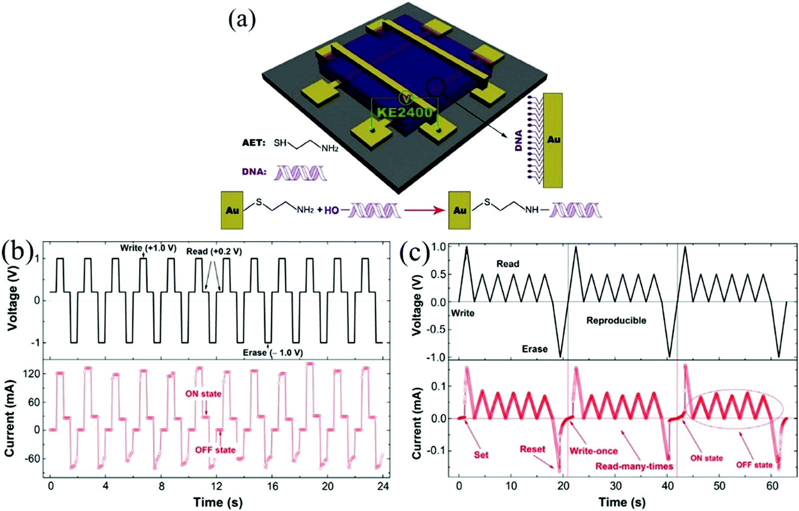 | ||
| Fig. 16 (a) The schematic of a biomemristor device with a Au/(DNA)n/Au structure. (b) The current response during the write–read–erase cycle-test process when a bias voltage was applied to the biomemristor device. (c) The write-once read many-times reproducible behavior of the biomemristor. Panels (a–c) reproduced with permission.79 Copyright 2015, Elsevier. | ||
In 2021, a new memristor with the Al/TiO2-few-layer graphene–DNA/Pt structure was introduced,134 which shows excellent resistive switching behavior with two-bit storage capacity in a single device. Two simultaneous operations can be achieved in this device, and it can save space for in-memory computing. Fig. 17a shows the schematic diagram of data storage and computing in memristors. This device with a crossbar structure is displayed in Fig. 17b. Two-bit computing operation can be achieved by using the crossbar structure contained word and bit lines in Fig. 17c. To display the feasibility of the device in logic circuit application, a memristor–transistor with an 8 × 8 memory array was simulated as in Fig. 17d. The pixel data were stored in the memristor array, in which each number indicated stored pixel data and the background color showed the pixel intensity. The Al/TiO2-few-layer graphene–DNA/Pt device with flexible multistate memory behavior can play a major role in the development of memristor-based chips. Moreover, multiple logical operations can be implemented in single memory cells. Therefore, this work provides guidance for the development of memristors with multistate logic operation, which show promise in artificial neuromorphic computing.
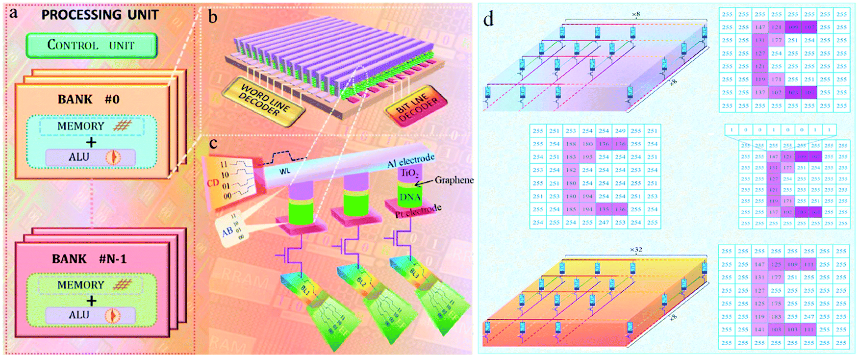 | ||
| Fig. 17 (a) The schematic diagram of in-memory computing in a biomemristor. (b) The schematic diagram of a biomemristor device with a Al/TiO2-few-layer graphene–DNA/Pt structure. (c) In-memory computing by 2-bit operation with word and bit lines. (d) The memristor array for stored pixel data. Panels (a–d) reproduced with permission.134 Copyright 2021, Elsevier. | ||
2.4 Cellulose-based biomemristors
It is well known that cellulose is usually used for wound dressings and cosmetic skincare, and it can also be used as a facial mask sheet. Cellulose is a sustainable natural material with excellent properties, e.g. renewability, low-cost and attractive mechanical properties, so it can act as the substrate and active layer of a photoelectric device.135–137 In 2014, Nagashima et al. designed and prepared a flexible biomemristor using a Ag-decorated cellulose nanofiber as the active layer, and the device shows a stable memory effect and high switching ratio (∼106).137 The schematic illustration and photograph of the biomemristor device prepared by Ag-decorated cellulose nanofiber paper in the Pt/Ti/SiO2/Si substrate are shown in Fig. 18a. During the experiment, 3–4 nm width 2,2,6,6-tetramethylpiperidine-1-oxyl (TEMPO)-oxidized cellulose nanofibers was used as the cellulose nanofiber paper (CNP) base matrix, and the CNP layer was fabricated on the Pt/Ti/SiO2/Si substrate by drop casting technology.138,139 The thickness of the Ag modified CNP can be regulated by changing the cellulose nanofiber slurry amount. The schematic illustration and photograph of the Ag-decorated cellulose nanofiber paper in an aluminium foil substrate (12 μm) prepared biomemristor are shown in Fig. 18b and c. This device has good flexibility, which can be twisted around a glass rod with diameter of ∼5 mm as in Fig. 18d. The I–V behavior curve of the biomemristor device on the aluminium foil substrate is shown in Fig. 18e. The aluminum foil substrate was used as the bottom electrode, which can conduct electricity and bend mechanically, and the resistive switching and durability were characterized. The mechanism was explained by the formation and fracture of Ag conductive filaments. This work shows that the Ag-decorated cellulose nanofiber paper prepared device displays ultra-flexible behavior, a high switching ratio and ultra-low operating voltage, which imply that cellulose nanofiber-based devices have wide application prospects in information storage.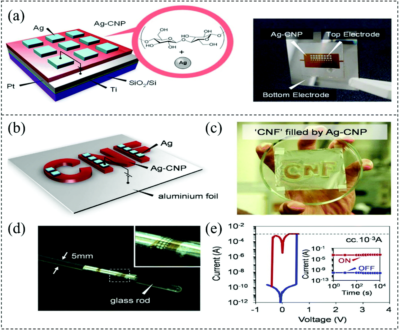 | ||
| Fig. 18 (a) The schematic illustration and photograph of a biomemristor device based on the Ag-decorated cellulose nanofiber paper. (b) The schematic illustration of a biomemristor device using the Ag-decorated cellulose nanofiber paper as the active layer on aluminium foil. (c) Optical picture of the corresponding device. (d) Optical picture of the device wrapped glass rod with about 5 mm diameter. (e) The I–V behavior curve of a biomemristor device. Panels (a–e) reproduced with permission.137 Copyright 2014, Nature publishing group. | ||
2.5 Plant-based biomemristors
Lignin is one of the most abundant natural biopolymers on earth, but it is often regarded as the waste of the paper industry because only a small part of it is used as low-value biomass. Lignin is widely sourced, cheap and biodegradable. Lignin with a complex chemical structure is an aromatic polymer, and its components mainly include some cellulose and hemicellulose.140 In 2017, Youngjun Park and Jang-Sik Lee reported a resistive switching device using biodegradable waste lignin as the active layer (∼100 nm).28Fig. 19a shows the schematic structure of lignin in lignocellulose, and the schematic structure and optical picture of the memristor device. The memory performance of the device is presented by the I–V behavior curve in Fig. 19b, and the stability and reliability were investigated by the tested rewritable cycle number in Fig. 19c. The test results show that the device has multilevel resistive switching behavior, and it can overcome the disadvantage of low density of organic memristors.141 The HRS presents three levels (10, 01, and 00) at different maximum VReset values (2, 2.5, and 3 V), and the low resistance state maintains state (11). This phenomenon may be due to the residual conductive filaments. A voltage (>2 V) can completely fracture the conductive filaments in the reset process, which will lead to the emergence of multi-level resistive switching. To confirm the feasibility of consecutive data storage operations at different multilevel resistance states, the multibit data storage capability was tested by using pulse measurement in Fig. 19d. When the positive pulses VReset (2.1, 2.6, 3.1 V) and negative pulse (−3 V) for 10 ms were applied to the biomemristor to form different HRS and LRS, respectively, a read pulse (0.2 V) was applied after each set and reset. The multilevel resistive state retention properties are shown in Fig. 19e, and there is no significant attenuation within 1000 s. This work shows that lignin is a very promising candidate material for biomemristors with multilevel high-density and biocompatibility. The flexibility of the biomemristor device implies that it has feasible applications in wearable electronics.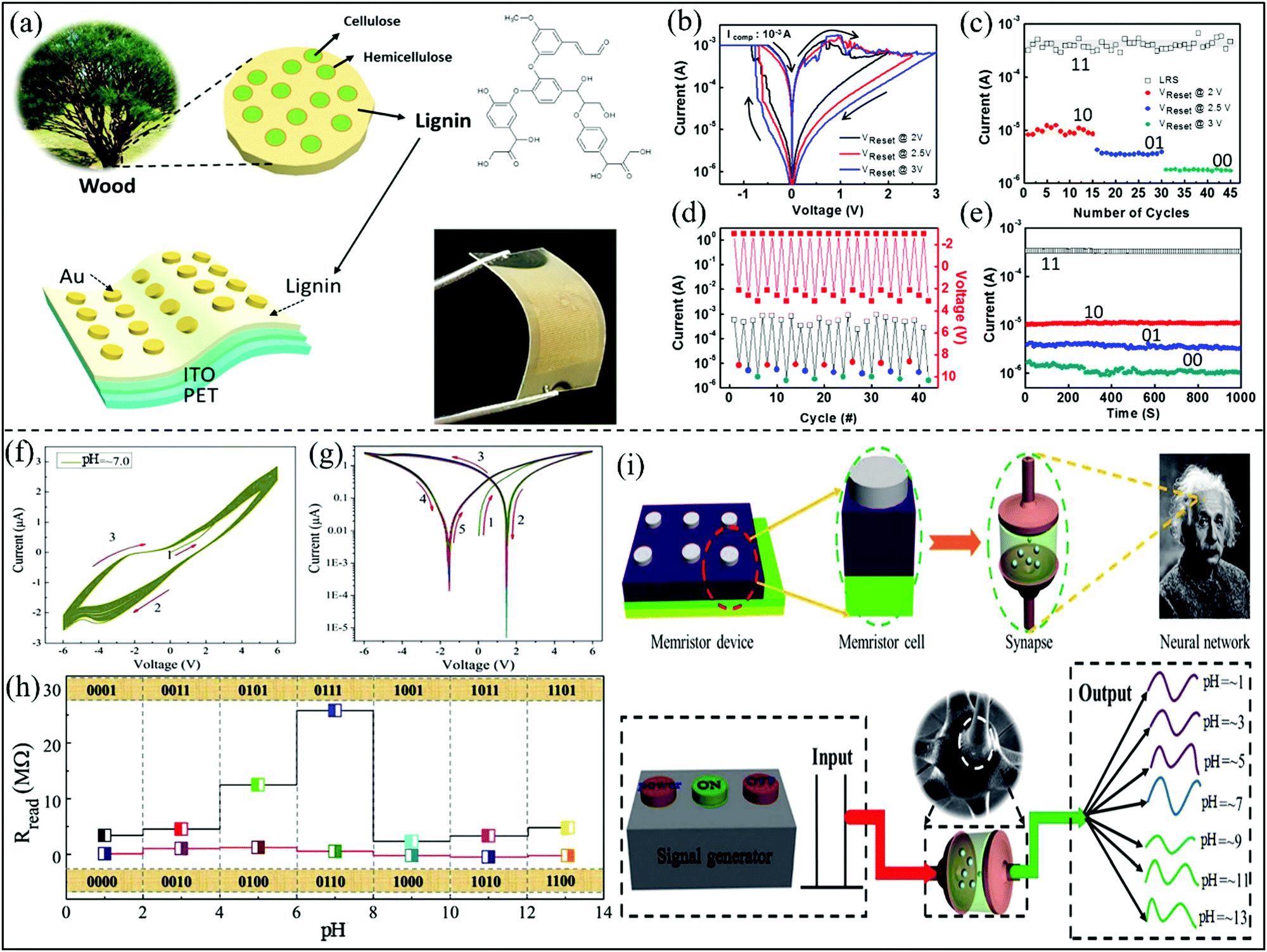 | ||
| Fig. 19 (a) The schematic structure of lignin in lignocellulose, and the schematic structure of a flexible memristor device. (b) I–V characteristic curve with difference reset voltages. (c) Multilevel resistance states by different reset voltages. (d) Pulse mode. (e) The biomemristor four state retention characteristics. Panels (a–e) reproduced with permission.28 Copyright 2017, American Chemical Society. (f) The I–V characteristic curves of the biomemristor based on an edible garlic under the pH = ∼7.0 condition. (g) Semilogarithmic scale I–V curve under the pH = ∼7.0 condition. (h) The multistate memory behavior by changing the pH value. (i) Schematic diagram of the memristor simulating the human brain. Panels (f–i) reproduced with permission.80 Copyright 2019, Royal Society of Chemistry. | ||
Garlic is one of the oldest cultivated plants, and it can be used as food and medicine. In 2019, we reported the edible garlic that can be used as the active layer of a memristor and its memory behavior can be modulated by pH.80 The memory behavior of the memristor with a Ag/garlic/FTO structure under pH = ∼7.0 condition is shown in Fig. 19f, and the corresponding semi-log scale I–V behavior is shown in Fig. 19g. It can be seen from the I–V behavior curve that the biomemristor has relatively good stability at pH = ∼7. More importantly, the I–V curve shows non-zero crossing characteristics, which implies that a capacitive-coupled memristive characteristic was formed. This resistance state of the biomemristor can be controlled by different pH conditions, as shown in Fig. 19h. The Ag/garlic/FTO device shows 14 logical states by adjusting pH, so the encoding and storage of information can be realized through four binary numbers. The redistribution of active ions and the formation and fracture of conductive filaments can be used to explain the non-zero crossing properties.12 A schematic diagram is present in Fig. 19i, in which the memristor can simulate the human brain. This research proves that the resistive switching behavior of the memristor device can be controlled by pH, which can be used for high density multistate memory, logic operation, and neuromorphic computing.
3. Biomemristor involved main mechanisms
As we all know, the development of a high-performance biomemristor must clearly understand its working mechanism. The reported mechanism mainly involves the formation and fracture of conductive filaments, ion migration, trap-assisted space-charge-limited conduction, electron hopping, Ohmic conduction, and so on. However, different materials may lead to different resistive switching mechanisms. Firstly, to understand the conduction mechanism of biomemristor devices, Rho et al. prepared a memristor using gold-decorated chitosan, and the charge transport was explained by trap-assisted space-charge-limited conduction in the HRS and formation/annihilation of conductive filaments in the LRS.86 It was considered that the resistive switching behavior can be attributed to the diffusion of ions and formation and fracture of metal conductive filaments, as shown in Fig. 20a. The conductive filament was caused by the electrochemical reaction between the electrode and dielectric layer. Electrochemical metallization anodic dissolution can occur at the interface between Ag and the dielectric layer. When an operating voltage was applied to the top electrode of tge device, it would produce Ag+ (Ag → Ag+ + e−) and migrate to the inert electrode Au, and then it was reduced to Ag near the Au electrode. When Ag ions entered into the dielectric layer of the device, the conductive filaments can be assembled in the SPE molecular chain.118,120 The opposite polarity voltage causes the narrowest part of the metal conductive filament to break, and further the biomemristor returns back to the initial state. Chen et al. fabricated a biomemristor device with a Ag/fibroin/Au structure, and the resistive switching mechanism was explained by Ag atom electrolytic migration formed conductive filaments.142 The migration of metal ions in the dielectric layer is a common phenomenon in electronics.143 To deeply understand the mechanism of resistive switching behavior, the relationship between the HRS and LRS versus temperature was studied. Surprisingly, it shows nonmetallic conductivity, in which the resistance of the device decreases with the increase of temperature for the HRS and LRS. The charge trapping/detrapping electron hopping between Ag islands was proposed to explain this phenomenon. To verify its rationality, the corresponding I–V curve was drawn on the log–log scale and fitted. The fitting results show that there are Ohmic traps and the space-charge-limited mechanism. The schematic diagram of the conductive model is presented in Fig. 20b when the biomemristor device is at the HRS and LRS.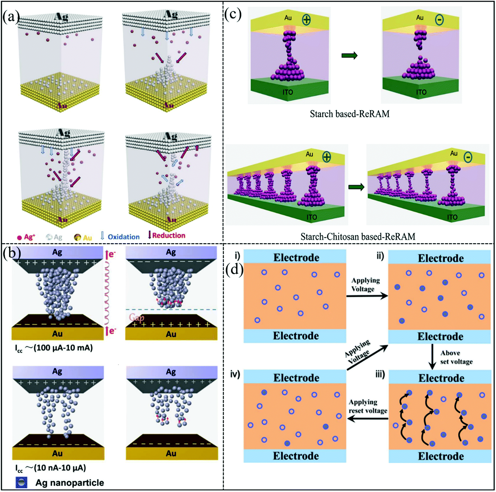 | ||
| Fig. 20 (a) Ion diffusion and formation and fracture of metal conductive filaments. Panel (a) reproduced with permission.86 Copyright 2021, American Chemical Society. (b) Charge trapping/detrapping and electron hopping. Panel (b) reproduced with permission.142 Copyright 2015, Wiley-VCH. (c) The formation and fracture of carbon filaments. Panel c reproduced with permission.127 Copyright 2016, American Chemical Society. (d) Hopping conduction. Panel (d) reproduced with permission.57 Copyright 2013, Wiley-VCH. | ||
Furthermore, an organic memristor device with a Cu/poly(ethylene glycol dimethacrylate/ITO structure was fabricated by Choi et al., and the carbon filaments can be directly observed from the transmission electron microscope (TEM) image.144 Lee et al. used a starch-chitosan composite to prepare a biomemristor,127 and the diagram of the working mechanism is shown in Fig. 20c; the resistive switching behavior of the biomemristor can be explained by formation and fracture of carbon filaments. Specifically, when a voltage was applied to the device, Joule heat would breakdown the weakest point of the solid polymer electrolyte (SPE) and produced voids. The applied voltage accelerated the local destruction of the SPE and formed a local carbon-rich region, and the voids surrounded to form a highly conductive region. Due to the poor conductivity of carbon rich filaments, the current flowing through would produce a lot of Joule heat, causing the temperature to increase. The fracture of the carbon conductive filament is due to the difference in thermal conductivity between carbon and SPE. For starch based biomemristors, the breaking of carbon filaments in the weakest point causes the device to switch from the LRS to the HRS. Compared with starch based biomemristors, the carbon atom density of starch and chitosan mixed devices was increased. When a large enough electric field was applied to the device, the Joule heat generated by the device was greater than the heat dissipation of the device, resulting in the damage of the weakest SPE structure and production of more voids. It leads to the formation of wide carbon conductive filaments in the SPE damaged area. Furthermore, the conductivity of this device is greatly improved. The application of a voltage with opposite polarity causes the local point fracture of carbon conductive filaments. Although nano carbon is a stable material, the specific fracture mechanism has been studied. The fracture of carbon nanotubes in an air atmosphere was caused by Joule heat, and stress at high temperatures can damage the structure.145,146 The rise in temperature and thinning in the middle of carbon nanotubes cause damage. Considering the complexity of the experimental process, the researcher comprehensively considered the length, diameter, volume, arrangement and other factors of carbon nanotubes, established the fracture model and verified it with experiments.147
Unlike conductive filaments, the electron hopping by Ag islands can also generate high current at the LRS. When the opposite polarity voltage was applied, the Ag atom at the bottom electrode will be dissolved and formed a positive charge region. Due to the interaction of Coulomb force, Ag ions move towards the Ag electrode. A gap can be formed between the bottom electrode and Ag nanoparticle, and the biomemristor can switch from the LRS to the HRS. Subsequently, Chen et al. explained charge transport of the Ag/sericin/Au structure memristor using hopping conduction and charge trapping/detrapping.57 This resistive switching behavior of the biomemristor device between the HRS and LRS was caused by the formation and fracture of the current path, as shown in Fig. 20d.
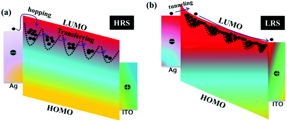
The trap center physical model based on the band energy structure was proposed to explain the resistive switching behavior of hydrogen-peroxide-modified egg albumen.148 Ions were randomly generated and distributed in the dielectric layer of the device during the process of protein denaturation. The energy of the trap is near the lowest unoccupied molecular orbital (LUMO) level. Electrons with kinetic energy have limited motion when jumping to the LUMO, causing the device to be in the HRS, as shown in Fig. 21a. The first energy level was fully occupied by electrons with the increase of applied voltage, and then the injected electrons would be transferred from the first energy level to the adjacent energy level because of the Kunlun and electron scattering effects.149 When the applied voltage exceeds VSet, all traps were occupied, and the difference between all trap energy levels and LUMO becomes smaller. Therefore, the injected electrons were transmitted to the trap energy level, resulting in the switching of the resistance state of the device from the HRS to the LRS in Fig. 21b.
 | ||
| Fig. 21 The physical model of trap centers. (a) HRS. (b) LRS. Panels a and b reproduced with permission.148 Copyright 2017, IOP Publishing. | ||
4. Conclusions and outlook
The properties of some typical biomemristors are shown in Table 1. By comparison, it can be found that protein materials exhibit relatively excellent memory performance (retention ∼106 s, HRS/LRS ∼107), which has become a research hotspot in recent years. Compared with inorganic material-based memristors with a similar structure and excellent performance, the dielectric layer of biomemristors is relatively thick, which will lead to a larger unit volume and affect the miniaturization of microelectronic devices.150,151 However, we believe that with the development of preparation technology, this obstacle will be overcome. Notably, the memory performance of protein materials can be improved by optimizing the device structure or by chemically modifying the protein materials.59,92,152 Importantly, biomemristor usually display flexibility with promise in the field of wearable electronic devices. In addition, a biomaterial-based biomemristor has also capacitive-coupled memristive properties.66,69,80 This electronic device with multiple properties lays the foundation for the development of future multifunctional electronic devices. In particular, the biomemristor prepared on a cellulose substrate further accelerates the development of wearable electronic devices.153 Therefore, the cellulose and protein may be the most potential candidate materials for the preparation of wearable biomemristors. Biomaterials can be compatible and biodegradable with living organisms, but biodegradable and fully biocompatible memristors have not been reported yet because electrodes are generally made of metals or doped metal oxides. Therefore, the development of biomemristors that are fully compatible with organisms and degradable must address electrode engineering problems by exploring novel functional materials that can replace metal electrodes.| Year | Device structure | Flexibility | Retention (s) | HRS/LRS ratio | Endurance (cycles) | Ref. |
|---|---|---|---|---|---|---|
| 2013 | Al/Silk/ITO | No | 1000 | 10 | 120 | 90 |
| 2015 | Al/Egg albumen/ITO | No | 10![[thin space (1/6-em)]](https://www.rsc.org/images/entities/char_2009.gif) 000 000 |
1000 | 600 | 91 |
| 2016 | Ag/Fibroin/Au | No | 1000 | 60 | 100 | 92 |
| 2016 | Au/Starch/ITO | Yes | 10000 |
— | — | 127 |
| 2017 | Ag/Silk fibroin/Au | Yes | 10000 |
100000 |
30 | 159 |
| 2017 | Ag/WK@AuNCs-SF/ITO | No | 10000 |
100 | 100 | 103 |
| 2017 | Ag/Leaves/Ti | Yes | 1000 | 50 | — | 32 |
| 2017 | ITO/Silkworm hemolymph/Al | No | 10000 |
1000 | 1000 | 94 |
| 2018 | Ag/DNA/ITO | No | 10000 |
100 | 200 | 153 |
| 2018 | Mg/Silk fibroin/W | Yes | 10000 |
10000 |
100 | 157 |
| 2018 | Ag/SF-CDs/ITO | Yes | 1000000 |
10000000 |
100 | 158 |
| 2019 | Ag/Walnut skin/ITO | No | 1300 | 2 | 10000 |
69 |
| 2019 | Ag/Garlic/FTO | No | — | 25 | 30000 |
80 |
| 2021 | Ag/Ag-Silk fibroin/ITO | Yes | 10000 |
∼120 | 100 | 59 |
| 2021 | Mo/C15H11O6–Graphene/Mo | No | — | 28 | 100 | 66 |
Fig. 22 summarizes the various functional materials used to develop biomemristors. Among these materials, a lot of work is devoted to the study of the memory behavior of protein materials, and there are few reports on other biomaterials. Therefore, we should pay attention to the memory properties of protein materials as well as other biomaterials in our follow-up work. In 2017, Kim et al. fabricated a wearable electrocardiogram monitor using ultrathin electrodes and p-MOS carbon nanotubes.154 The electrical device is designed to conform to the dynamic surface of human skin, showing excellent flexibility through repeated deformation tests. The schematic diagram of the wearable heart monitoring is shown in Fig. 23a, which consists of three parts, namely the electrocardiogram sensing electrode, the p-MOS carbon nanotube signal amplifier and the color-tunable organic light-emitting diode. Advances in science and technology have led to the development of many artificial organs while being challenging. This flexible electronic and e-skin can be used in human health monitoring as shown in Fig. 23b and c. This new application prospect requires materials with functional elements, and lightweight and flexibility properties.155,156
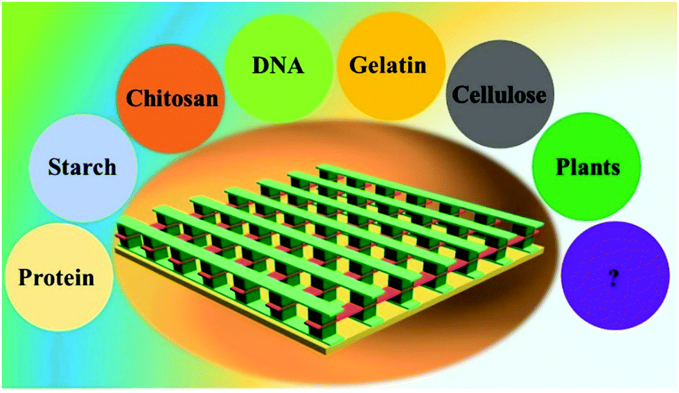 | ||
| Fig. 22 The various functional materials used to develop biomemristors. | ||
 | ||
| Fig. 23 (a) Wearable cardiac-monitoring. Panel (a) reproduced with permission.154 Copyright 2017, American Chemical Society. (b) Schematic illustration of flexible electronics for human health monitoring. Panel (b) reproduced with permission.155 Copyright 2020, Elsevier. (c) The application prospect of e-skins by body heat. Panel c reproduced with permission.156 Copyright 2019, Elsevier. | ||
Significant progress has been made in the field of wearable biomemristors in recent years. Biomemristor devices are expected to grow rapidly over the next decade. However, there are many challenges to be solved in the field of wearable biomemristors, and technical bottlenecks need to be broken to achieve perfect wearability. A clear understanding of the charge transport mechanism of biomemristive devices in complex environments is very important for the development of high-performance biomemristive devices. Some of the challenges faced by researchers in the wearable system field can only be addressed through technological innovation or interdisciplinary research. At the same time, this interdisciplinary research will accelerate the development of advanced wearable systems. For example, materials scientists should work on developing novel functional biomaterials with memory properties to meet the requirements of wearable devices. Researchers in other fields should work on developing wearable biopower sources, connecting wires between devices, wearable displays, encoding processing of information, and so on. In addition, to solve the problems faced by each device, it is also necessary to solve the problems faced by the integrated connection technology between the devices. In particular, close participation of the medical industry personnel in the wearable field is also required. After a wearable electronic system obtains health data, the biomemristor system periodically transmits these data to medical staff which will assess our health status. Clearly, wearable systems show fascinating application prospects. In order to realize commercial wearable systems, researchers in various fields need to work hard to address various challenges that bioelectronics face in wearable systems.153,157–159
In summary, the research progress and applications of biomemristors in neural synapses, image recognition, and logic computing are discussed in detail to promote the development of biomemristors in wearable electronic devices. Due to the unique properties of biomaterials such as lightweight, flexibility, easy access, abundant resources, biodegradability, and biocompatibility, biomemristors show attractive application prospects in the field of wearable electronic devices with memory behaviors. These biomaterials can also be used to prepare biosensors, biocapacitors, and biodetectors, which lay the scientific foundation for the development of wearable systems. Therefore, biomaterials are expected to play an important role in wearable biomemristors.
Author contributions
S. Mao and B. Sun drafted the review manuscript. B. Sun made revisions. G. Zhou, T. Guo and J. Wang made some discussions. Y. Zhao gave some useful suggestions. All authors gave their approval to the final version of the manuscript.Conflicts of interest
The authors declare no conflict of interest.Acknowledgements
The authors gratefully acknowledge financial support from the Sichuan Science and Technology Program (Grant No. 2020YJ0086), the Fundamental Research Funds for the Central Universities (Grant No. 2682021CX076), and the National Key R&D Program of China (No. 2017YFE0301401), and Y. Zhao is grateful to the Fujian Normal University for the financial support of the talent project.References
- L. Chua, IEEE Trans. Circuit Theory, 1971, 18, 507–519 Search PubMed.
- D. B. Strukov, G. S. Snider, D. R. Stewart and R. S. Williams, Nature, 2008, 453, 80–83 CrossRef CAS PubMed.
- L. Chua, Semicond. Sci. Technol., 2014, 29, 104001 CrossRef.
- J. Borghetti, G. S. Snider, P. J. Kuekes, J. J. Yang, D. R. Stewart and R. S. Williams, Nature, 2010, 464, 873–876 CrossRef CAS PubMed.
- S. H. Jo, T. Chang, I. Ebong, B. B. Bhadviya, P. Mazumder and W. Lu, Nano Lett., 2010, 10, 1297–1301 CrossRef CAS PubMed.
- B. Sun, G. Zhou, T. Guo, Y. N. Zhou and Y. A. Wu, Nano Energy, 2020, 75, 104938 CrossRef CAS.
- J. Kolar, J. M. Macak, K. Terabe and T. Wagner, J. Mater. Chem. C, 2014, 2, 349–355 RSC.
- G. U. Siddiqui, M. M. Rehman and K. H. Choi, J. Mater. Chem. C, 2017, 5, 5528–5537 RSC.
- G. U. Siddiqui, M. M. Rehman, Y.-J. Yang and K. H. Choi, J. Mater. Chem. C, 2017, 5, 862–871 RSC.
- S. Ranjan, B. Sun, G. Zhou, Y. A. Wu, L. Wei and Y. N. Zhou, ACS Appl. Nano Mater., 2020, 3, 5045–5052 CrossRef CAS.
- G. Zhou, B. Sun, X. Hu, L. Sun, Z. Zou, B. Xiao, W. Qiu, B. Wu, J. Li, J. Han, L. Liao, C. Xu, G. Xiao, L. Xiao, J. Cheng, S. Zheng, L. Wang, Q. Song and S. Duan, Adv. Sci., 2021, 2003765 CrossRef CAS.
- B. Sun, Y. Chen, M. Xiao, G. Zhou, S. Ranjan, W. Hou, X. Zhu, Y. Zhao, S. A.-T. Redfern and Y. N. Zhou, Nano Lett., 2019, 19, 6461–6465 CrossRef CAS PubMed.
- G. Sassine, C. Nail, P. Blaise, B. Sklenard, M. Bernard, R. Gassilloud, A. Marty, M. Veillerot, C. Vallée, E. Nowak and G. Molas, Adv. Electron. Mater., 2018, 1800658 Search PubMed.
- R. Wang, H. Li, L. Zhang, Y.-J. Zeng, Z. Lv, J.-Q. Yang, J.-Y. Mao, Z. Wang, Y. Zhou and S.-T. Han, J. Mater. Chem. C, 2019, 7, 10203–10210 RSC.
- B. Zhu, H. Wang, Y. Liu, D. Qi, Z. Liu, H. Wang, J. Yu, M. Sherburne, Z. Wang and X. Chen, Adv. Mater., 2016, 28, 1559–1566 CrossRef CAS PubMed.
- X. Guan, W. Hu, M. A. Haque, N. Wei, Z. Liu, A. Chen and T. Wu, Adv. Funct. Mater., 2018, 28, 1704665 CrossRef.
- R. Wang, J.-Q. Yang, J.-Y. Mao, Z.-P. Wang, S. Wu, M. Zhou, T. Chen, Y. Zhou and S.-T. Han, Adv. Intell. Syst., 2020, 2, 2000055 CrossRef.
- C.-H. Huang, K. Matsuzaki and K. Nomura, Appl. Phys. Lett., 2020, 116, 023503 CrossRef.
- M. Sivan, Y. Li, H. Veluri, Y. Zhao, B. Tang, X. Wang, E. Zamburg, J. F. Leong, J. X. Niu, U. Chand and A. V.-Y. Thean, Nat. Commun., 2019, 10, 5201 CrossRef PubMed.
- W. Wang, M. Wang, E. Ambrosi, A. Bricalli, M. Laudato, Z. Sun, X. D. Chen and D. Ielmini, Nat. Commun., 2019, 10, 81 CrossRef CAS PubMed.
- Y. Park and J. S. Lee, ACS Nano, 2017, 11, 8962–8969 CrossRef CAS PubMed.
- Y. Sun, D. Wen, Y. Xie, F. Sun, X. Mo, J. Zhu and H. Sun, J. Phys. Chem. Lett., 2019, 10, 7745–7752 CrossRef CAS PubMed.
- F. Pan, S. Gao, C. Chen, C. Song and F. Zeng, Mater. Sci. Eng., R, 2014, 83, 1–59 CrossRef.
- Q. Luo, X. Xu, H. Liu, H. Lv, T. Gong, S. Long, Q. Liu, H. Sun, W. Banerjee, L. Li, J. Gao, N. Lu, S. S. Chung, J. Li and M. Liu, IEEE International Electron Devices Meeting, 2015 Search PubMed.
- Y. Yang, B. Chen and W. D. Lu, Adv. Mater., 2015, 27, 7720–7727 CrossRef CAS PubMed.
- Y.-X. Zhou, Y. Li, N. Duan, Z.-R. Wang, K. Lu, M.-M. Jin, L. Cheng, S.-Y. Hu, T.-C. Chang, H.-J. Sun, K.-H. Xue and X.-S. Miao, Adv. Electron. Mater., 2018, 1800229 CrossRef.
- J.-L. Meng, T.-Y. Wang, Z.-Y. He, L. Chen, H. Zhu, L. Ji, Q.-Q. Sun, S.-J. Ding, W.-Z. Bao, P. Zhou and D. W. Zhang, Mater. Horiz., 2021, 8, 538–546 RSC.
- Y. Park and J.-S. Lee, ACS Appl. Mater. Interfaces, 2017, 9, 6207–6212 CrossRef CAS PubMed.
- D. Ielmini, F. Nardi and C. Cagli, Appl. Phys. Lett., 2010, 96, 053503 CrossRef.
- B. Sun, G. Zhou, L. Sun, H. Zhao, Y. Chen, F. Yang, Y. Zhao and Q. Song, Nanoscale Horiz., 2021, 6, 939–970 RSC.
- J. X. Zhu, W. L. Zhou, Z. Q. Wang, H. Y. Xu, Y. Lin, W. Z. Liu, J. G. Ma and Y. C. Liu, RSC Adv., 2017, 7, 32114–32119 RSC.
- B. Sun, S. Zhu, S. Mao, P. Zheng, Y. Xia, F. Yang, M. Lei and Y. Zhao, J. Colloid Interface Sci., 2018, 513, 774–778 CrossRef CAS PubMed.
- S. P. Park, Y. J. Tak, H. J. Kim, J. H. Lee, H. Yoo and H. J. Kim, Adv. Mater., 2018, 30, 1800722 CrossRef PubMed.
- H. Bae, D. Kim, M. Seo, I. K. Jin, S.-B. Jeon, H. M. Lee, S.-H. Jung, B. C. Jang, G. Son, K. Yu, S.-Y. Choi and Y.-K. Choi, Adv. Mater. Technol., 2019, 4, 1900151 CrossRef CAS.
- D. Yang, H. Yang, X. Guo, H. Zhang, C. Jiao, W. Xiao, P. Guo, Q. Wang and D. He, Adv. Funct. Mater., 2020, 30, 2004514 CrossRef CAS.
- Y. Kim, W. Jeon, M. Kim, J. H. Park, C. S. Hwang and S.-S. Lee, Appl. Mater. Today, 2020, 19, 100569 CrossRef.
- Q. Wang, G. Niu, S. Roy, Y. Wang, Y. Zhang, H. Wu, S. Zhai, W. Bai, P. Shi, S. Song, Z. Song, Y. H. Xie, Z. G. Ye, C. Wenger, X. Meng and W. Ren, J. Mater. Chem. C, 2019, 7, 12682–12687 RSC.
- Y. Huang, Z. Shen, Y. Wu, X. Wang, S. Shang, X. Shi and H. Zeng, RSC Adv., 2016, 6, 17867–17872 RSC.
- Z. Chen, Y. Yu, L. Jin, Y. Li, Q. Li, T. Li, J. Li, H. Zhao, Y. Zhang, H. Dai and J. Yao, J. Mater. Chem. C, 2020, 8, 2178–2185 RSC.
- H. W. Du, T. Wan, B. Qu, F. Y. Cao, Q. R. Lin, N. Chen, X. Lin and D. W. Chu, ACS Appl. Mater. Interfaces, 2017, 9, 20762–20770 CrossRef CAS PubMed.
- T. Aziz, S. Wei, Y. Sun, L.-P. Ma, S. Pei, S. Dong, W. Ren, Q. Liu, H.-M. Cheng and D.-M. Sun, Nanoscale, 2021, 13, 2448–2455 RSC.
- T. Paul, P. K. Sarkar, S. Maiti and K. K. Chattopadhyay, ACS Appl. Electron Mater., 2020, 2, 3667–3677 CrossRef CAS.
- X. Wang, B. Sun, X. Li, B. Guo, Y. Zeng, S. Mao, S. Zhu, Y. Xia, S. Tian and W. Luo, Ceram. Int., 2018, 44, 18108–18112 CrossRef CAS.
- X. Sun, C. Wu, Y. Shuai, X. Pan, W. Luo, T. You, A. Bogusz, N. Du, Y. Li and H. Schmidt, ACS Appl. Mater. Interfaces, 2016, 8, 32956–32962 CrossRef CAS PubMed.
- F. Zeng, Y. Guo, W. Hu, Y. Tan, X. Zhang, J. Feng and X. Tang, ACS Appl. Mater. Interfaces, 2020, 12, 23094–23101 CrossRef CAS PubMed.
- Q. Liao, Y. Wang, Z. Lv, Z. Xiong, J. Chen, G. P. Wang, S.-T. Han and Y. Zhou, Org. Electron., 2021, 90, 106062 CrossRef CAS.
- S. Wang, Y. Xiong, X. Dong, J. Sha, Y. Wu, W. Li and Y. Wang, J. Alloys Compd., 2021, 874, 159884 CrossRef CAS.
- K. Liao, P. Lei, M. Tu, S. Luo, T. Jiang, W. Jie and J. Hao, ACS Appl. Mater. Interfaces, 2021, 13, 32606–32623 CrossRef CAS PubMed.
- J. Zhou, W. Li, Y. Chen, Y. Lin, M. Yi, J. Li, Y. Qian, Y. Guo, K. Cao, L. Xie, H. Ling, Z. Ren, J. Xu, J. Zhu, S. Yan and W. Huang, Adv. Mater., 2021, 33, 2006201 CrossRef CAS PubMed.
- L. Yuan, S. Liu, W. Chen, F. Fan and G. Liu, Adv. Electron. Mater., 2021, 2100432 CrossRef CAS.
- H.-L. Park and T.-W. Lee, Org. Electron., 2021, 98, 106301 CrossRef CAS.
- X. Yan, X. Li, Z. Zhou, J. Zhao, H. Wang, J. Wang, L. Zhang, D. Ren, X. Zhang, J. Chen, C. Lu, P. Zhou and Q. Liu, ACS Appl. Mater. Interfaces, 2019, 11, 18654–18661 CrossRef CAS PubMed.
- Y. Segui, B. Ai and H. Carchano, J. Appl. Phys., 1976, 47, 140–143 CrossRef CAS.
- R. S. Potember, T. O. Poehler and D. O. Cowan, Appl. Phys. Lett., 1979, 34, 405–407 CrossRef CAS.
- C. O. Baker, B. Shedd, R. J. Tseng, A. A. Martinez-Morales, C. S. Ozkan, M. Ozkan, Y. Yang and R. B. Kaner, ACS Nano, 2011, 5, 3469–3474 CrossRef CAS PubMed.
- C. Y. Shi, J. J. Wang, M. R.-A. Sushko, W. Qiu, X. B. Yan and X. Y. Liu, Adv. Funct. Mater., 2019, 29, 1904777 CrossRef CAS.
- H. Wang, F. Meng, Y. Cai, L. Zheng, Y. Li, Y. Liu, Y. Jiang, X. Wang and X. Chen, Adv. Mater., 2013, 25, 5498–5503 CrossRef CAS PubMed.
- H.-L. Park, M.-H. Kim, H. Kim and S.-H. Lee, Adv. Electron. Mater., 2021, 7, 2100299 CrossRef CAS.
- Y. Zhang, F. Han, S. N. Fan and Y. P. Zhang, ACS Biomater. Sci. Eng., 2021, 7, 3459–3468 CrossRef CAS PubMed.
- K. Qian, N. Viet Cuong, T. Chen and P. S. Lee, J. Mater. Chem. C, 2016, 4, 9637–9645 RSC.
- X. He, J. Zhang, W. Wang, W. Xuan, X. Wang, Q. Zhang and J. Luo, ACS Appl. Mater. Interfaces, 2016, 8, 10954–10960 CrossRef CAS PubMed.
- N. R. Hosseini and J. S. Lee, Adv. Funct. Mater., 2015, 25, 5586–5592 CrossRef CAS.
- Y. Zhang, S. Fan and Y. Zhang, Mater. Horiz., 2021, 8, 3281–3294 RSC.
- S.-Y. Min and W.-J. Cho, Int. J. Mol. Sci., 2021, 22, 773 CrossRef CAS PubMed.
- G. Kook, S. Jeong, M. K. Kim, S. W. Lee, N. Choi and H. J.-J. Lee, Adv. Mater. Technol., 2020, 5, 1900991 CrossRef CAS.
- B. Sun, T. Guo, G. Zhou, J. Wu, Y. Chen, Y. N. Zhou and Y. A. Wu, ACS Appl. Bio Mater, 2021, 4, 1976–1985 CrossRef CAS PubMed.
- B. Sun, M. Xiao, G. Zhou, Z. Ren, Y. N. Zhou and Y. A. Wu, Mater. Today Adv., 2020, 6, 100056 CrossRef.
- L. Wang and D. Wen, Micromachines, 2019, 10, 1–12 Search PubMed.
- S. Mao, X. Zhang, B. Sun, B. Li, T. Yu, Y. Chen and Y. Zhao, Electron. Mater. Lett., 2019, 15, 547–554 CrossRef CAS.
- Y. Qi, B. Sun, G. Fu, T. Li, S. Zhu, L. Zheng, S. Mao, X. Kan, M. Lei and Y. Chen, Chem. Phys., 2018, 516, 168–174 CrossRef.
- B. Guo, B. Sun, W. Hou, Y. Chen, S. Zhu, S. Mao, L. Zheng, M. Lei, B. Li and G. Fu, RSC Adv., 2019, 9, 12436–12440 RSC.
- G. D. Zhou, B. Sun, A. Zhou and B. Wu, Curr. Appl. Phys., 2017, 17, 235–239 CrossRef.
- L. Zheng, B. Sun, S. Mao, S. Zhu, P. Zheng, Y. Zhang, M. Lei and Y. Zhao, ACS Appl. Bio Mater., 2018, 1, 496–501 CrossRef CAS PubMed.
- M. M. Rehman, H. M.-M. ur Rehman, W. Y. Kim, S. S.-H. Sherazi, M. W. Rao, M. Khan and Z. Muhammad, ACS Appl. Electron. Mater., 2021, 3, 2832–2861 CrossRef CAS.
- M.-K. Kim and J.-S. Lee, ACS Appl. Mater. Interfaces, 2018, 10, 10280–10286 CrossRef CAS PubMed.
- Y. Guo, W. Hu, F. Zeng, C. Zhang, Y. Peng and Y. Guo, Org. Electron., 2020, 83, 105750 CrossRef CAS.
- J.-Y. Lam, G.-W. Jang, C.-J. Huang, S.-H. Tung and W.-C. Chen, ACS Sustainable Chem. Eng., 2020, 8, 5100–5106 CrossRef CAS.
- B. K. Murgunde and M. K. Rabinal, Org. Electron., 2017, 48, 276–284 CrossRef CAS.
- S. Qin, R. Dong, X. Yan and Q. Du, Org. Electron., 2015, 22, 147–153 CrossRef CAS.
- S. Mao, B. Sun, T. Yu, W. Mao, S. Zhu, Y. Ni, H. Wang, Y. Zhao and Y. Chen, New J. Chem., 2019, 43, 9634–9640 RSC.
- I. A. Tayeb, F. Zhao, J. M. Abdullah and K. Y. Cheong, J. Mater. Chem. C, 2021, 9, 1437–1450 RSC.
- J. Wang, C. Shi, M. L. Sushko, J. Lan, K. Sun, J. Zhao, X. Y. Liu and X. Yan, ACS Appl. Mater. Interfaces, 2021, 13, 39641–39651 CrossRef CAS PubMed.
- N. Raeis-Hosseini, Y. Park and J.-S. Lee, Adv. Funct. Mater., 2018, 1800553 CrossRef.
- D. Kuzum, S. Yu and H. P. Wong, Nanotechnology, 2013, 24, 382001 CrossRef PubMed.
- C. Zhang, W. B. Ye, K. Zhou, H.-Y. Chen, J.-Q. Yang, G. Ding, X. Chen, Y. Zhou, L. Zhou, F. Li and S.-T. Han, Adv. Funct. Mater., 2019, 29, 1808783 CrossRef.
- N. Raeis-Hosseini and J. Rho, ACS Appl. Mater. Interfaces, 2021, 13, 5445–5450 CrossRef CAS PubMed.
- Y. Lee, J. Park, A. Choe, S. Cho, J. Kim and H. Ko, Adv. Funct. Mater., 2020, 30, 1904523 CrossRef CAS.
- H. Wang, B. Zhu, X. Ma, Y. Hao and X. Chen, Small, 2016, 12, 2715–2719 CrossRef CAS PubMed.
- L. Wang, D. Chen, K. Jiang and G. Shen, Chem. Soc. Rev., 2017, 46, 6764–6815 RSC.
- C. Mukherjee, M. K. Hota, D. Naskar, S. C. Kundu and C. K. Maiti, Phys. Status Solidi A, 2013, 210, 1797–1805 CrossRef CAS.
- Y.-C. Chen, H.-C. Yu, C.-Y. Huang, W.-L. Chung, S.-L. Wu and Y.-K. Su, Sci. Rep., 2015, 5, 10022 CrossRef CAS PubMed.
- B. Sun, D. Liang, X. Li and P. Chen, J. Mater. Sci.: Mater. Electron., 2016, 27, 3957–3962 CrossRef CAS.
- O. Basha, R. Shpringer, C. M. Argov and E. Yeger-Lotem, Nucleic Acids Res., 2018, 46(D1), D522–D526 CrossRef CAS PubMed.
- L. Wang and D. Wen, Sci. Rep., 2017, 7, 17418 CrossRef PubMed.
- W. Qiu, A. Patil, F. Hu and X. Y. Liu, Small, 2019, 15, 1903948 CrossRef CAS PubMed.
- Y. Song, Z. F. Lin, L. Q. Kong, Y. Xing, N. B. Lin, Z. S. Zhang, B. H. Chen and X. Y. Liu, Adv. Funct. Mater., 2017, 27, 1700628 CrossRef.
- Y. Wang, D. Aurelio, W. Y. Li, P. Tseng, Z. Z. Zheng, M. Li, D. L. Kaplan, M. Liscidini and F. G. Omenetto, Adv. Mater., 2017, 29, 1702769 CrossRef PubMed.
- M. K. Hota, M. K. Bera, B. Kundu, S. C. Kundu and C. K. Maiti, Adv. Funct. Mater., 2012, 22, 4493–4499 CrossRef CAS.
- N. Raeis-Hosseini and J.-S. Lee, J. Electroceram., 2017, 39, 223–238 CrossRef CAS.
- H. Tao, D. L. Kaplan and F. G. Omenetto, Adv. Mater., 2012, 24, 2824–2837 CrossRef CAS PubMed.
- B. W. Zhu, H. Wang, W. R. Leow, Y. R. Cai, X. J. Loh, M. Y. Han and X. D. Chen, Adv. Mater., 2016, 28, 4250–4265 CrossRef CAS PubMed.
- G. Chen, N. Matsuhisa, Z. Liu, D. Qi, P. Cai, Y. Jiang, C. Wan, Y. Cui, W. R. Leow, Z. Liu, S. Gong, K.-Q. Zhang, Y. Cheng and X. Chen, Adv. Mater., 2018, 30, 1800129 CrossRef PubMed.
- Y. Xing, C. Shi, J. Zhao, W. Qiu, N. Lin, J. Wang, X. Yan, W. Yu and X. Liu, Small, 2017, 13, 1702390 CrossRef PubMed.
- K. J. Waldron, J. C. Rutherford, D. Ford and N. J. Robinson, Nature, 2009, 460, 823–830 CrossRef CAS PubMed.
- F. B. Meng, B. Sana, Y. G. Li, Y. J. Liu, S. Lim and X. D. Chen, Small, 2014, 10, 277–283 CrossRef CAS PubMed.
- T. Li, W. Hu and D. Zhu, Adv. Mater., 2010, 22, 286–300 CrossRef CAS PubMed.
- L. Qin, J. Jang, L. Huang and C. A. Mirkin, Small, 2007, 3, 86–90 CrossRef CAS PubMed.
- C. Zhang, J. Shang, W. Xue, H. Tan, L. Pan, X. Yang, S. Guo, J. Hao, G. Liu and R.-W. Li, Chem. Commun., 2016, 52, 4828–4831 RSC.
- Y. C. Yang, P. Gao, S. Gaba, T. Chang, X. Q. Pan and W. Lu, Nat. Commun., 2012, 3, 732 CrossRef PubMed.
- X. N. Zhao, H. Y. Xu, Z. Q. Wang, L. Zhang, J. G. Ma and Y. C. Liu, Carbon, 2015, 91, 38–44 CrossRef CAS.
- S. K. Jang, S. Kim, M. S. Salman, J.-R. Jang, Y. M. Um, L. Tan, J.-H. Park, W.-S. Choe and S. Lee, Chem. Mater., 2018, 30, 781–788 CrossRef CAS.
- G. D. Zhou, Z. J. Ren, L. D. Wang, B. Sun, S. K. Duan and Q. L. Song, Mater. Horiz., 2019, 6, 1877–1882 RSC.
- B. C. Jang, Y. Nam, B. J. Koo, J. Choi, S. G. Im, S. H.-K. Park and S. Y. Choi, Adv. Funct. Mater., 2018, 28, 1704725 CrossRef.
- T. Chang, S.-H. Jo and W. Lu, ACS Nano, 2011, 5, 7669–7676 CrossRef CAS PubMed.
- C. Y. Shi, J. L. Lan, J. J. Wang, S. Zhang, Y. H. Lin, S. H. Zhu, A. E. Stegmann, R. Yu, X. B. Yan and X. Y. Liu, Adv. Funct. Mater., 2020, 30, 2002882 CrossRef CAS.
- B. Wang, W. Yang, J. McKittrick and M. A. Meyers, Prog. Mater. Sci., 2016, 76, 229–318 CrossRef CAS.
- H. Tu, R. Yu, Z. Lin, L. Zhang, N. Lin, W. D. Yu and X. Y. Liu, Adv. Funct. Mater., 2016, 26, 9032–9043 CrossRef CAS.
- N. E. Kurland, T. Dey, C. Wang, S. C. Kundu and V. K. Yadavalli, Adv. Mater., 2014, 26, 4431–4437 CrossRef CAS PubMed.
- W.-Y. Huang, Y.-C. Chang, Y.-F. Sie, C.-R. Yu, C.-Y. Wu and Y.-L. Hsu, ACS Appl. Polym. Mater., 2021, 3, 4478–4484 CrossRef CAS.
- W. Sun, B. Gao, M. F. Chi, Q. F. Xia, J. J. Yang, H. Qian and H. Q. Wu, Nat. Commun., 2019, 10, 3453 CrossRef PubMed.
- L. Wang, Y. Zhang and D. Wen, Nanomaterials, 2021, 11, 1973 CrossRef CAS PubMed.
- N. R. Hosseini and J. S. Lee, ACS Nano, 2015, 9, 419–426 CrossRef PubMed.
- H. H.-D. Ho, T. M. Le, N. K. Pham and N. D. Cuong, J. Nanomater., 2021, 1–7 Search PubMed.
- Y. H. Liu, L. Q. Zhu, P. Feng, Y. Shi and Q. Wan, Adv. Mater., 2015, 27, 5599–5604 CrossRef CAS PubMed.
- C.-W. Liew, S. Ramesh, K. Ramesh and A. K. Arof, J. Solid State Electrochem., 2012, 16, 1869–1875 CrossRef CAS.
- M. Kumar, T. Tiwari and N. Srivastava, Carbohydr. Polym., 2012, 88, 54–60 CrossRef CAS.
- N. Raeis-Hosseini and J. S. Lee, ACS Appl. Mater. Interfaces, 2016, 8, 7326–7332 CrossRef CAS PubMed.
- E. Guibal, Sep. Purif. Technol., 2004, 38, 43–74 CrossRef CAS.
- R. C. Atkinson and R. M. Shiffrin, Psychol. Learn. Motiv, 1968, 2, 89–195 Search PubMed.
- J. Zhao, Z. Zhou, Y. Zhang, J. Wang, L. Zhang, X. Li, M. Zhao, H. Wang, Y. Pei, Q. Zhao, Z. Xiao, K. Wang, C. Qin, G. Wang, H. Li, B. Ding, F. Yan, K. Wang, D. Ren, B. Liu and X. Yan, J. Mater. Chem. C, 2019, 7, 1298–1306 RSC.
- R. S. Zucker and W. G. Regehr, Annu. Rev. Physiol., 2002, 64, 355–405 CrossRef CAS PubMed.
- B. Yurke, A. J. Turberfield, A. P.-M. Jr, F. C. Simmel and J. L. Neumann, Nature, 2000, 406, 605–608 CrossRef CAS PubMed.
- B. Sun, L. Wei, H. Li, X. Jia, J. Wu and P. Chen, J. Mater. Chem. C, 2015, 3, 12149–12155 RSC.
- B. Sun, S. Ranjan, G. Zhou, T. Guo, Y. Xia, L. Wei, Y. N. Zhou and Y. A. Wu, Mater. Today Adv., 2021, 9, 100125 CrossRef CAS.
- A. C. Siegel, S. T. Phillips, M. D. Dickey, N. Lu, Z. Suo and G. M. Whitesides, Adv. Funct. Mater., 2010, 20, 28–35 CrossRef CAS.
- W. J. Hyun, O. O. Park and B. D. Chin, Adv. Mater., 2013, 25, 4729–4734 CrossRef CAS PubMed.
- K. Nagashima, H. Koga, U. Celano, F. Zhuge, M. Kanai, S. Rahong, G. Meng, Y. He, J. De Boeck, M. Jurczak, W. Vandervorst, T. Kitaoka, M. Nogi and T. Yanagida, Sci. Rep., 2014, 4, 5532 CrossRef CAS PubMed.
- H. Koga, T. Saito, T. Kitaoka, M. Nogi, K. Suganuma and A. Isogai, Biomacromolecules, 2013, 14, 1160–1165 CrossRef CAS PubMed.
- K. Missoum, M. N. Belgacem and J. Bras, Materials, 2013, 6, 1745–1766 CrossRef PubMed.
- D. Kai, M. J. Tan, P. L. Chee, Y. K. Chua, Y. L. Yap and X. J. Loh, Green Chem., 2016, 18, 1175–1200 RSC.
- G. Khurana, P. Misra and R. S. Katiyar, Carbon, 2014, 76, 341–347 CrossRef CAS.
- H. Wang, Y. Du, Y. Li, B. Zhu, W. R. Leow, Y. Li, J. Pan, T. Wu and X. Chen, Adv. Funct. Mater., 2015, 25, 3825–3831 CrossRef CAS.
- R. Waser, R. Dittmannn, G. Staikov and K. Szot, Adv. Mater., 2009, 21, 2632–2663 CrossRef CAS.
- B.-H. Lee, H. Bae, H. Seong, D.-I. Lee, H. Park, Y. J. Choi, S.-G. Im, S. O. Kim and Y.-K. Choi, ACS Nano, 2015, 9, 7306–7313 CrossRef CAS PubMed.
- K. Mølhave, S. B. Gudnason, A. T. Pedersen, C. H. Clausen, A. Horsewell and P. Bøggild, Nano Lett., 2006, 6, 1663–1668 CrossRef PubMed.
- W. Wei, Y. Liu, Y. Wei, K. Jiang, L.-M. Peng and S. Fan, Nano Lett., 2007, 7, 64–68 CrossRef PubMed.
- V. Mirjalili and P. Hubert, Compos. Sci. Technol., 2010, 70, 1537–1543 CrossRef CAS.
- G. Zhou, Y. Yao, Z. Lu, X. Yang, J. Han, G. Wang, X. Rao, P. Li, Q. Liu and Q. Song, Nanotechnology, 2017, 28, 425202 CrossRef PubMed.
- H. Yan, C. Chuang, A. Zhugayevych, S. Tretiak, F. W. Dahlquist and G. C. Bazan, Adv. Mater., 2015, 27, 1908–1911 CrossRef CAS PubMed.
- X. Wu, R. Ge, P. A. Chen, H. Chou, Z. Zhang, Y. Zhang, S. Banerjee, M. H. Chiang and J. C. Lee, Adv. Mater., 2019, 31, 1806790 CrossRef PubMed.
- R. D. Nikam, K. G. Rajput and H. Hwang, Small, 2021, 17, 2006760 CrossRef CAS PubMed.
- H. Wang, B. W. Zhu, H. Wang, X. H. Ma, Y. Hao and X. D. Chen, Small, 2016, 12, 3360–3365 CrossRef CAS PubMed.
- H.-Y. Jeng, T.-C. Yang, L. Yang, J. G. Grote, H.-L. Chen and Y.-C. Hung, Org. Electron., 2018, 54, 216–221 CrossRef CAS.
- J. H. Koo, S. Jeong, H. J. Shim, D. Son, J. Kim, D. C. Kim, S. Choi, J. I. Hong and D. H. Kim, ACS Nano, 2017, 11, 10032–10041 CrossRef CAS PubMed.
- D. Wang, L. Wang, Z. Lou, Y. Zheng, K. Wang, L. Zhao, W. Han, K. Jiang and G. Shen, Nano Energy, 2020, 78, 105252 CrossRef CAS.
- R. Tian, Y. Liu, K. Koumoto and J. Chen, Joule, 2019, 3, 1399–1403 CrossRef.
- X. Ji, L. Song, S. Zhong, Y. Jiang, K. G. Lim, C. Wang and R. Zhao, J. Phys. Chem. C, 2018, 121, 16909–16915 CrossRef.
- Z. Lv, Y. Wang, Z. Chen, L. Sun, J. Wang, M. Chen, Z. Xu, Q. Liao, L. Zhou, X. Chen, J. Li, K. Zhou, Y. Zhou, Y. J. Zeng, S. T. Han and V. A.-L. Roy, Adv. Sci., 2018, 5, 1800714 CrossRef PubMed.
- J. Yong, B. Hassan, Y. Liang, K. Ganesan, R. Rajasekharan, R. Evans, G. Egan, O. Kavehei, J. Li, G. Chana, B. Nasr and E. Skafidas, Sci. Rep., 2017, 7, 14731 CrossRef PubMed.
| This journal is © The Royal Society of Chemistry 2022 |