
Materials and design strategies for stretchable electroluminescent devices
Jisu
Yoo†
a,
Shi
Li†
b,
Dae-Hyeong
Kim
 *cde,
Jiwoong
Yang
*bf and
Moon Kee
Choi
*ag
*cde,
Jiwoong
Yang
*bf and
Moon Kee
Choi
*ag
aDepartment of Materials Science and Engineering, Ulsan National Institute of Science and Technology (UNIST), Ulsan 44919, Republic of Korea. E-mail: mkchoi@unist.ac.kr
bDepartment of Energy Science and Engineering, Daegu Gyeongbuk Institute of Science and Technology (DGIST), Daegu 42988, Republic of Korea. E-mail: jiwoongyang@dgist.ac.kr
cCenter for Nanoparticle Research, Institute for Basic Science (IBS), Seoul 08826, Republic of Korea. E-mail: dkim98@snu.ac.kr
dSchool of Chemical and Biological Engineering, Institute of Chemical Process, Seoul National University, Seoul 08826, Republic of Korea
eDepartment of Materials Science and Engineering, Seoul National University, Seoul 08826, Republic of Korea
fEnergy Science and Engineering Research Center, Daegu Gyeongbuk Institute of Science and Technology (DGIST), Daegu 42988, Republic of Korea
gGraduate School of Semiconductor Materials and Devices Engineering, Center for Future Semiconductor Technology (FUST), Ulsan National Institute of Science and Technology (UNIST), Ulsan 44919, Republic of Korea
First published on 24th May 2022
Abstract
Stretchable displays have recently received increasing attention as input and/or output interfaces for next-generation human-friendly electronic systems. Stretchable electroluminescent (EL) devices are a core component of stretchable displays, and they can be classified into two types, structurally stretchable EL devices and intrinsically stretchable EL devices, according to the mechanism for achieving their stretchability. We herein present recent advances in materials and design strategies for stretchable EL devices. First, stretchable devices based on ultrathin EL devices are introduced. Ultrathin EL devices are mechanically flexible like thin paper, and they can become stretchable through various structural engineering methods, such as inducing a buckled structure, employing interconnects with stretchable geometries, and applying origami/kirigami techniques. Secondly, intrinsically stretchable EL devices can be fabricated by using inherently stretchable electronic materials. For example, light-emitting electrochemical cells and EL devices with a simpler structure using alternating current have been developed. Furthermore, novel stretchable semiconductor materials have been presented for the development of intrinsically stretchable light-emitting diodes. After discussing these two types of stretchable EL devices, we briefly discuss applications of deformable EL devices and conclude the review.
 Jisu Yoo | Jisu Yoo received her BS (2019) degree from the Department of Materials Science and Engineering at Ulsan National Institute of Science and Technology (UNIST). Under the supervision of Prof. Moon Kee Choi, she is working on the fabrication and application of intrinsically stretchable electroluminescent devices. |
 Shi Li | Shi Li received her BE (2017) degree from the School of Engineering at Lishui University of China and her ME (2020) degree from the School of Science at Zhejiang Sci-Tech University of China. She is now pursuing her PhD degree in the Department of Energy Science and Engineering under the guidance of Prof. Jiwoong Yang at Daegu Gyeongbuk Institute of Science and Technology (DGIST). Her recent research focuses on the fabrication of high-performance optoelectronic devices for wearable light-based biosensors. |
 Dae-Hyeong Kim | Dae-Hyeong Kim is a professor in the School of Chemical and Biological Engineering at Seoul National University, an associate director of the Center for Nanoparticle Research of the Institute for Basic Science (IBS), and an associate editor of Science Advances. He received his BS (2000) and MS (2002) degrees from the School of Chemical Engineering at Seoul National University. He obtained his PhD (2009) from the Department of Materials Science and Engineering at the University of Illinois at Urbana–Champaign. Since he joined the faculty of the School of Chemical and Biological Engineering at Seoul National University in 2011, he has focused on stretchable and soft electronics for biomedical and energy applications. |
 Jiwoong Yang | Jiwoong Yang is an assistant professor in the Department of Energy Science and Engineering of Daegu Gyeongbuk Institute of Science and Technology (DGIST). He received his BS (2011) and PhD (2016) in Chemical and Biological Engineering from Seoul National University under the guidance of Prof. Taeghwan Hyeon. From 2017 to 2019, he was a postdoctoral researcher at Lawrence Berkeley National Laboratory under the guidance of Dr Haimei Zheng. His research interests include synthesis and characterization of nanocrystals for energy and electronic devices. |
 Moon Kee Choi | Moon Kee Choi is an assistant professor in the Department of Materials Science and Engineering of Ulsan National Institute of Science and Technology (UNIST). She received her BS (2009) and PhD (2016) in Chemical and Biological Engineering from Seoul National University under the guidance of Prof. Dae-Hyeong Kim. She conducted her postdoctoral research in the lab of Prof. Seung-Wuk Lee at UC Berkeley. Now, she is focusing on the development of next-generation optoelectronic devices and biomedical electronics with deformable form factors. |
1. Introduction
Displays are a key component of electronic devices that help visualize various electrical data.1–5 Over the past decades, advances in displays have been mainly focused on increasing the color gamut, screen size, and definition of displays.6–16 As a result, the resolution and color purity of displays have reached almost the limits detectable by the human eye.17–20 In recent years, thus, there has been a growing demand for another type of innovative display, such as the one that allows for users to freely change the display shape according to their intended purposes (e.g., enhancing portability, multitasking, and space utilization).21–28 Conforming to this trend, flexible displays have been introduced in mobile phones, monitors, and televisions, and lately foldable smartphones have been developed. More recently, there has been a demand for developing next-generation flexible displays with a higher degree of deformation freedom beyond curved/bendable and rollable/foldable displays, such as those with twisting and stretching capabilities (Fig. 1a). Stretchable displays have been highlighted, which are regarded as indispensable user interfaces for next-generation human-friendly electronic systems including bio-integrated electronic devices such as wearable, attachable, and implantable devices.29–31 It is envisioned that these stretchable displays can conformally fit to curvilinear surfaces of traditional objects, providing additional functionalities as “displays on things”. The deformability of displays can also enhance their wearability to be conformally attached to the human skin. Furthermore, stretchable displays require less space when carried, making them more portable. Hence, numerous attempts, in terms of the development of new materials and application of novel device designs, have been made to confer stretchability to displays.32–35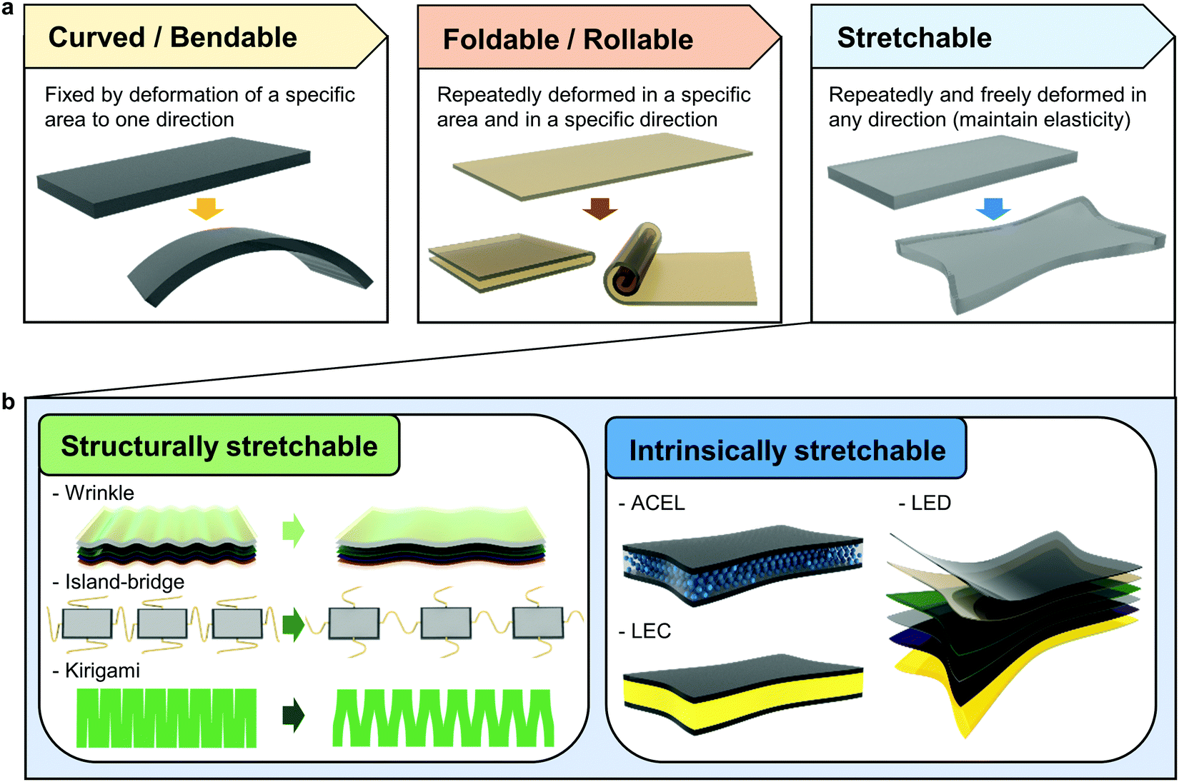 | ||
| Fig. 1 Schematic illustration of flexible electroluminescent devices. (a) Progress in the development of flexible EL devices. (b) Categories of stretchable EL devices. | ||
The first flexible organic light-emitting diodes (OLEDs) were reported in 1992 by Gustafsson et al.36 In 2008, Nokia proposed a prototype phone called Morph using flexible displays. Later, flexible displays were integrated into commercial curved televisions (Samsung Electronics, 2013) and smart phones with curved edges (Samsung Electronics, 2015) to provide a wide field of view and additional user interface support, respectively. However, the curvature of these displays was fixed according to the shape of the device framework. In 2009, Samsung Electronics commercialized their foldable display smartphones that can withstand folding cycles exceeding 200![[thin space (1/6-em)]](https://www.rsc.org/images/entities/char_2009.gif) 000 folds in the folding test. Recent foldable displays usually employ ultrathin encapsulation layers (e.g., transparent polyimide or glass) to endure severe mechanical stress imposed on the hinge part of the displays (bending radius: >1.4 mm) during such repetitive folding tests. In addition, 65 inch rollable displays, with 5.8 mm total thickness and 50 mm bending radius, were commercialized in 2020 by LG Electronics. The shape of the commercialized flexible displays reported to date can only be changed by the one-directional pre-programmed motion of specific parts. Considering this limitation, stretchable displays can present new opportunities in the display industry with regard to novel form factors. Despite such a demand, the research on stretchable displays is still in its early stage. Therefore, it is necessary to develop stretchable displays with three-dimensional deformability, high luminance, and high efficiency. Furthermore, it is greatly demanding to utilize existing device technologies (scaling up, pixelation, and active-matrix integration) for stretchable displays to be compatible with established semiconductor manufacturing processes.37,38
000 folds in the folding test. Recent foldable displays usually employ ultrathin encapsulation layers (e.g., transparent polyimide or glass) to endure severe mechanical stress imposed on the hinge part of the displays (bending radius: >1.4 mm) during such repetitive folding tests. In addition, 65 inch rollable displays, with 5.8 mm total thickness and 50 mm bending radius, were commercialized in 2020 by LG Electronics. The shape of the commercialized flexible displays reported to date can only be changed by the one-directional pre-programmed motion of specific parts. Considering this limitation, stretchable displays can present new opportunities in the display industry with regard to novel form factors. Despite such a demand, the research on stretchable displays is still in its early stage. Therefore, it is necessary to develop stretchable displays with three-dimensional deformability, high luminance, and high efficiency. Furthermore, it is greatly demanding to utilize existing device technologies (scaling up, pixelation, and active-matrix integration) for stretchable displays to be compatible with established semiconductor manufacturing processes.37,38
Electroluminescent (EL) devices are an essential component of displays, serving as either backlight sources with color filters or multiplexed light-emitting pixels.39 Hence, the development of high-performance stretchable EL devices should precede the development of stretchable displays. This review presents recent advances in materials and device designs for the development of stretchable EL devices. We categorize stretchable EL devices into two types: (i) structurally stretchable EL devices and (ii) intrinsically stretchable EL devices (Fig. 1b). Structurally stretchable EL devices achieve stretchability through various structural engineering methods by applying special designs to ultrathin EL devices. The structural engineering methods include a buckling technique, an island and bridge design, and a folding and cutting design for origami/kirigami. In contrast, intrinsically stretchable EL devices use inherently stretchable electronic materials to gain intrinsic deformability. In the early days, stretchable alternating current EL (ACEL) devices, a simple capacitive type of EL device operated with alternating current, have been reported. Recently, stretchable semiconductor materials have been developed for intrinsically stretchable light-emitting electrochemical cells (LECs) and light-emitting diodes (LEDs), which are more compatible with commercial displays based on inorganic and/or organic LEDs operated using direct current (DC). After discussing these kinds of stretchable EL devices, we present a brief review of the applications of deformable EL devices.
2. Structurally stretchable EL devices
The first type of stretchable EL device is the structurally-engineered stretchable EL device. Ultrathin EL devices, although made of conventional thin-film-based electronic materials, can exhibit a high degree of deformability through various methods for engineering of the device structure (e.g., buckling, pop-up, serpentine, and origami/kirigami). This part discusses such structural engineering methods and introduces representative device examples of each method.2.1 Ultrathin EL devices with buckled structures
One of the most efficient structural engineering methods to make a stretchable device is to reduce the device thickness and adopt wrinkles in the device.40–49 When bent, the inner and outer parts of the solid material experience compression and tension, respectively.50 These induced strains are linearly proportional to the material thickness.51,52 Minimal thickness allows facile release of internal stress in the device during deformation, reducing the likelihood of cracks in the active layers and improving the device stability.53 Moreover, with the reduced thickness of brittle materials, it is easier to locate all the brittle materials near the neutral mechanical plane54—the region between the inner part (in compression) and the outer part (in tension) of bent materials where the compressive and tensile stresses cancel each other out. The materials in the neutral mechanical plane are not under stress and thus are free from mechanical fractures. Thus, LEDs with ultrathin thickness have been developed for deformable EL devices. Most LEDs share similar device structures (Fig. 1b and 2a), because they utilize electroluminescence in which semiconductor materials produce photons by using externally applied electron–hole pairs. Electrons and holes are injected into charge injection layers (electron injection layer, EIL, and hole injection layer, HIL) and charge transport layers (electron transport layer, ETL, and hole transport layer, HTL) from electrodes (cathodes and anodes), and then into the emission layer (EML) for light emission via radiative recombination. Because the thickness of each active layer in LEDs is only a few tens of nanometers, they can be developed to have an ultrathin form factor. Further, by using the ultrathin device, a stretchable device can also be fabricated. Applying pre-strain to the device and releasing the pre-strain leads to the formation of a wrinkled structure in the ultrathin device. The wrinkles can be flattened under external tensile strains and the buckled device can become stretchable. Due to the ultrathin thickness and the neutral mechanical plane design, the buckled device can avoid mechanical fractures even during repetitive stretching cycles.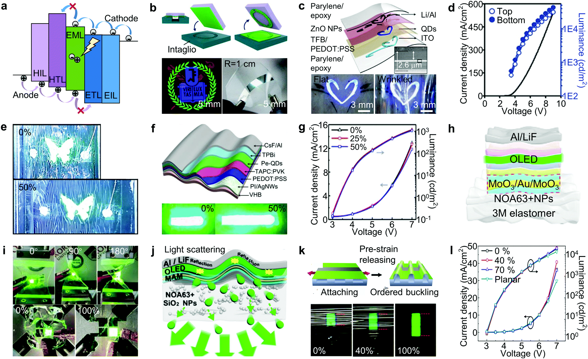 | ||
| Fig. 2 Ultrathin EL devices with buckled structures. (a) Schematic illustration of the energy diagram and light generation mechanism in LEDs. (b) Schematic of the intaglio transfer printing technique. High-resolution red, green, and blue pixels (bottom left) and pixelated white QLEDs (bottom right) fabricated using this technique. (c) Schematic (top) and photographs (bottom) of a wearable QLED in the flat and wrinkled states. Reproduced with permission from ref. 55. Copyright 2015, Springer Nature. (d) J–V–L characteristics of transparent QLEDs. (e) Photographs of ultrathin stretchable transparent QLEDs with up to 50% deformation. Reproduced with permission from ref. 56. Copyright 2018, Wiley-VCH. (f) Schematic of an ultrathin PeLED with a PI/AgNW composite electrode. The ultrathin flexible PeLED on a wrinkled surface has a stretchable form factor (bottom). (g) J–V–L characteristics of a stretchable PeLED under different strains. Reproduced with permission from ref. 57. Copyright 2019, Wiley-VCH. (h) Schematic of a geometrically stretchable organic light-emitting diode (GSOLED). (i) Images of the GSOLEDs under various deformations, including twisting (top) and 2D stretching (bottom). (j) Schematic of the optical light scattering for a MoO3/Au/MoO3 (MAM) electrode with SiO2 NP embedded substrates. Reproduced with permission from ref. 58. Copyright 2021, Springer Nature. (k) Schematic of the fabrication of stretchable OLEDs with an ordered-buckling profile. Images of a stretchable OLED fabricated on a 200% pre-stretched substrate with strains from 0% to 100% (bottom). (l) J–V–L characteristics of the OLEDs under different stretching conditions. Reproduced with permission from ref. 59. Copyright 2016, Springer Nature. | ||
Choi et al. reported wearable quantum dot (QD) LEDs (QLEDs) with an ultrathin form factor.55 They developed an intaglio transfer printing technique for patterning ultrahigh-resolution pixels (∼2460 pixels per inch) of red, green, and blue QDs. The high interfacial energy difference between QDs/intaglio trenches and QDs/stamps allowed ∼100% transfer yield and improved the definition of the patterns regardless of their size, shape, and complexity (Fig. 2b). This printing technique could fabricate full-color QLED arrays with red, green, and blue sub-pixels. Geometric separation of sub-pixels could provide balanced white light, because it is helpful to inhibit the energy transfer between QDs of different colors in conventional white QLEDs.60–64 Because the active layer of the ultrathin QLEDs were positioned in the neutral mechanical plane of the entire device (∼300 nm active layer with double encapsulation layers of ∼1.1 μm; total thickness ∼2.6 μm), high mechanical flexibility could be achieved (Fig. 2c). The ultrathin QLEDs with high brightness (∼14000 cd m−2) maintained their EL characteristics on various curvilinear surfaces (e.g., human skin) even under various mechanical deformations such as bending, folding, and wrinkling (bottom images of Fig. 2c), and showed consistent brightness after more than 1000 cycles of ∼20% stretching.
By engineering the device structure, ultrathin QLEDs could be fabricated to be highly transparent (>84% in visible light).56 A thin alumina layer (∼2 nm), introduced on the ZnO electron transport layer, protects QDs and charge transport layers from plasma damage, allowing transparent and conductive ITO to be used as top and bottom electrodes. In addition, the alumina layer balanced the electron/hole injection into the QDs by blocking an excess electron transport over the hole transport, leading to superior device characteristics (bottom: ∼43000 cd m−2, top: ∼30000 cd m−2, total: ∼73000 cd m−2 at 9 V) (Fig. 2d). Despite using brittle ITO electrodes in ultrathin transparent QLEDs, they could withstand various mechanical deformations such as 1000 bending cycles (bending radii 0.05–13 mm), 50% stretching of the buckled QLED (Fig. 2e), compression on human skin, and folding on the edge of a slide glass without degradation of the EL performance.
In addition to QLEDs, LEDs employing perovskite nanocrystals (NCs) can adopt ultrathin designs. For example, Li et al. reported stretchable wavy organometal–halide–perovskite NC LEDs (PeLEDs) using ultrathin electrodes made of a transparent polyimide (PI) and silver nanowire (AgNW) composite mixed with titania (Fig. 2f).57 The ultrathin PeLEDs were transferred onto a pre-stretched elastic substrate, and a wavy structure of the PeLED was fabricated by releasing the pre-strain. Titania nanoparticles act as a protective layer on the AgNW networks without affecting their conductivity and optical transparency. Ultrathin (1–2 μm), smooth (roughness of 0.796 nm), and flexible PI/AgNW composite electrodes were developed for an ultrathin PeLED with a total thickness of ∼3 μm. The stretchable PeLED showed a high degree of deformability, such as bendability with a bending radius of ∼70 μm and a stretchability of 50% (bottom image of Fig. 2f). Even under tensile strain, the device showed excellent EL characteristics (turn-on voltage of 3.2 V, maximum current efficiency of 8.91 cd A−1 at 7 V) (Fig. 2g).
Stretchable devices based on ultrathin OLEDs can also be fabricated.65–69 Choi et al. developed a transparent MoO3 (15 nm)/Au (14 nm)/MoO3 (5 nm) electrode to fabricate a geometrically stretchable OLED (GSOLED) (Fig. 2h).58 Because of the deep work function of MoO3 and Au, the energy level of the Au electrode (5.25 eV) matches the energy level of the hole injection layer (N,N′-bis-(1-naphthyl)-N,N′-diphenyl-1,1′-biphenyl-4,4′-diamine (NPB)), which enabled high EL performance (external quantum efficiency of ∼22.3%) with minimum efficiency roll-off. A wrinkled type of GSOLED could be fabricated on a highly flexible composite substrate, consisting of a pre-strained 3M elastomer and an ultra-violet curable polymer (Norland Optical Adhesive 63 (NOA63)), by releasing the pre-strain. The wavy GSOLED could withstand various mechanical deformations, including 1D torsion at various angles (1–180°) (top images of Fig. 2i), 2D stretching with various biaxial strains (0–100%) (bottom images of Fig. 2i), and 3D deformation by stretching on a golf ball (42.7 mm diameter), showing uniform light emission without color change. In order to avoid the deterioration of OLED performance caused by heat accumulation on the thick elastomer,58 silicon dioxide nanoparticles were incorporated in the NOA63 substrate. The silicon dioxide nanoparticles have high thermal conductivity70 (1.3 W m−1 K−1) and thus were helpful for the heat dissipation from the device. Also, the nanoparticles could improve the optical output coupling efficiency by ∼10% (Fig. 2j) via the Mie scattering effect.71
Buckling can be precisely controlled with a desired periodicity to manage the mechanical characteristics of stretchable LEDs.72,73 For example, Yin et al. developed an effective laser-programmable buckling process to achieve stretchable OLEDs with ordered buckling profiles.59 The ultrathin OLED was selectively attached on top of a pre-stretched elastomer with a 1D grating structure. After releasing the pre-strain, the unattached part of the OLED formed a periodical pop-up structure (top schematic of Fig. 2k). The buckling period of the OLED was determined by the interval of the 1D grating, which could be made by using femtosecond laser ablation. The buckled OLED could be repeatedly stretched up to 15000 times with a small luminance attenuation (∼16%) under a tensile strain of ∼20%. The tensile strain that the device could withstand was proportional to the pre-strain of the elastomeric substrate. For example, stretchable OLEDs with 100% stretchability could be obtained on a substrate with 200% pre-strain (bottom images of Fig. 2k). Regardless of the applied strain, stretchable OLEDs exhibited a constant turn-on voltage around ∼3 V (Fig. 2l).
2.2 Ultrathin EL devices with island–bridge structures
Through structural engineering, stretchable LED arrays using rigid EL devices can be developed.74–77 Although each light-emitting unit is not flexible, the entire array can be stretched using submillimeter-size LEDs and stretchable interconnection. During mechanical deformation, the interconnects are deformed instead of LEDs and release the stress applied to the device, avoiding mechanical failures.Park et al. designed metal mesh electrodes with arc-shaped pop-up bridge structures to interconnect ultra-small (100 μm × 100 μm) inorganic LEDs (ILEDs) to form a 16 × 16 deformable ILED array (Fig. 3a).78 The ultrathin geometry (∼2.5 μm) enabled the array to be flexible, and the device array is compatible with conventional microfabrication techniques. The ILED island array interconnected with flat metal mesh electrodes was placed on a pre-strained poly(dimethylsiloxane) (PDMS) substrate. After releasing the pre-strain, the metal mesh electrodes underwent out-of-plane flexion to form a non-coplanar arc-shaped bridge structure. The curvature change of the arc-shaped bridge electrode could accommodate mechanical deformations. Based on finite element simulations, the maximum strain in the ILED island was only 0.17%, while the entire ILED array was subjected to 24% strain. Moreover, the devices showed excellent mechanical stability upon stretching up to ∼22% strain (Fig. 3b). The arc-shaped pop-up bridge interconnects successfully dissipated the induced stress.
 | ||
| Fig. 3 Ultrathin EL devices with island–bridge structures and with cuts and folds. (a) Image of a 16 × 16 stretchable passive-matrix ILED array on a PDMS rubber substrate interconnected by arc-shaped bridge structures. (b) I–V characteristics of an ILED display under various applied strains. Reproduced with permission from ref. 78. Copyright 2009, The American Association for the Advancement of Science (AAAS). (c) Image of a 6 × 6 stretchable inorganic LED array with serpentine-shaped bridges (inset) with 46% stretch along the diagonal direction. (d) Voltages at 20 μA current of the ILED array for different cycles of 75% stretch along the horizontal direction. Reproduced with permission from ref. 79. Copyright 2010, Springer Nature. (e) Optical image of a deformable 9.1 inch full-color AMOLED display in the convex and flat states (inset). (f) Schematic of a low-temperature vacuum thermoforming process. Reproduced with permission from ref. 80. Copyright 2017, Wiley-VCH. (g) Cross-sectional SEM image of stretchable substrates with surface relief island–bridge structures with elastic pillar arrays (top). The bottom image shows a photograph of stress-relief substrates stretched to 35% (from the blue arrow to the white arrow). (h) J–L characteristics of stretchable OLEDs under various applied strains. Reproduced with permission from ref. 81. Copyright 2020, American Chemical Society. (i) Optical images of 3D OLEDs with candle flame structures under ambient light (left) and in the dark (right). Reproduced with permission from ref. 82. Copyright 2018, Wiley-VCH. (j) Photograph of a 3 inch distortion-free auxetic meta-display placed on a spherical surface with a radius of curvature of 40 mm. (k) Optical image of a meta-display with kirigami cutting patterns under uniaxial stretching and before stretching (inset). Reproduced with permission from ref. 83. Copyright 2022, Wiley-VCH. (l) Developable nets for an ellipsoid using the computational wrapping design of non-stretchable commercial EL panels. The right image shows the EL of the wrapped panel. Reproduced with permission from ref. 84. Copyright 2020, The American Association for the Advancement of Science (AAAS). | ||
The serpentine-shape structure is another successful design for deformable island–bridge type arrays.85–89 For instance, Kim et al. developed a stretchable LED array with sub-50 micron-scale ILEDs (μ-ILEDs) and serpentine-shape interconnects fabricated on a pre-stretched (∼20%) PDMS substrate (Fig. 3c).79 Compared to the arc-shaped pop-up structure, the non-coplanar serpentine interconnection could effectively dissipate the multi-axial strains at a higher strain level. Therefore, the μ-ILED array endured various mechanical deformations, including 100000 cycles of ∼75% uniaxial stretching (Fig. 3d), diagonal stretching of ∼46%, corkscrew twisting of 720°, bending, and folding.
The strategy of structural designs has also been applied to commercial products. In 2017, Samsung Electronics developed a prototype device of 9.1 inch 3D convex and/or concave shape active-matrix OLED (AMOLED) displays (Fig. 3e).80 The displays were composed of tiny OLEDs as individual pixel islands interconnected with island–bridge structures. A low-temperature polycrystalline silicon thin-film transistor (TFT) backplane was employed for the display. The AMOLED panel was integrated into numerous micron-size cavities on a polyimide substrate, using the low-temperature thermoforming process (Fig. 3f). Like a balloon, the display could be stretched over ∼5%, leading to the formation of the convex and/or concave shape with 10 mm displacement that could also be restored to an original flat state. Moreover, even with such deformability, the brightness of the display could reach 300 cd m−2.
The use of stress relief substrates is helpful to reduce the stress on the active area of devices. Lim et al. designed stretchable OLED arrays on stress-relief stretchable substrates interconnected using a compact zigzag-shaped structure (Fig. 3g).81 In this work, the pixel islands were suspended on the elastic substrates that can disperse the stress on the active areas of devices, thus providing greater stretchability than the flat island–bridge structure. The elastic substrates consisted of PDMS micropillar arrays and SU-8 plates supported by PDMS pillars on the PDMS substrates (top image in Fig. 3g). The stretchable OLEDs could be easily fabricated on the SU-8 plates and bridges through a simple thermal evaporation process, allowing the devices to possess up to 90% of the active area in the non-stretched state. When the device was stretched, the bridges between the plates stretched, making the active area functional until 35% stretching (Fig. 3h). Finite element method simulations supported that the external stress on the pillars supporting the SU-8 was much smaller than that on the pillars connected to the PDMS. The stretchable OLED arrays with 30 nm Al2O3 encapsulation layers maintained the stretchability while showing an operational half-life time of 50 h at 5 V with a duty cycle of 50%.
2.3 Ultrathin EL devices with cuts and folds
Origami/kirigami methods and the resulting 3D structures, inspired by ancient paper art, have attracted extensive research attention due to their compatibility with ultrathin flexible electronics. Devices using origami/kirigami designs and structures can be reversibly transformed between non-stretchable 2D panels and complex 3D structures. The simple and low-cost origami/kirigami strategy can endow ultrathin devices with a high stretchability far beyond the deformation limit of the material or device itself and planar devices with various 3D deformabilities such as multi-directional bending, curling, and twisting capability. Recently, such an origami/kirigami strategy has been applied to flexible EL devices.For example, Kim et al. fabricated ultrathin OLEDs with origami/kirigami designs.82 Large-area (>15 cm2) 2D patterned OLEDs were cut, curled, and assembled according to the pre-defined cut and fold patterns to construct the desired 3D candle flame without degradation of the original device performance. The patterned slits allowed for the planar OLEDs to be bent out-of-plane, and thus distribute the induced strain and withstand a large amount of stress. By simply integrating different folding and cutting patterns, planar OLEDs could be transformed into a variety of 3D structures, including pop-up globe lamps and candle flames (Fig. 3i). Moreover, the 3D space can be occupied by the transformed 3D EL device more efficiently, which thus leads to better light exploitation and higher brightness.
Origami/kirigami techniques can effectively improve the stretchability of EL devices. Jang et al. prepared a 3-inch reconfigurable auxetic meta-display consisting of micro-LEDs with a kirigami-based auxetic circuit board on a rigid PI film, achieving ∼24.5% stretchability while minimizing image distortion during stretching (Fig. 3j).83 Micro-LEDs were transferred to a meta-printed circuit board (PCB) with a Poisson's ratio of −1 using the roll transfer technique. During stretching, the meta-PCB with the kirigami cutting lines formed a geometry of rotational squares and hinge structures (Fig. 3k). Adjacent rigid squares rotated at the same angles in the opposite directions. At the same time, the hinges connecting the square pixels were uniformly extended to the stretching direction, allowing the display to exhibit isotropic stretching with high image fidelity. The kirigami cutting lines with both ends of circular holes can reduce local strain near the hinge, resulting in an elongation five times greater than the elastic limit of the PI film while retaining effective electrical properties. Moreover, the distortion-free displays can be conformably attached to various surfaces with non-zero Gaussian curvatures, including facial skin, concave and convex surfaces, and spherical surfaces with a radius of 40 mm.
Origami/kirigami-applied ultrathin devices also exhibit as high conformability to curved surfaces as elastic materials. The computer-aided approach can advance the design of curved LEDs that fits the morphology of various 3D objects by employing highly complex origami/kirigami designs. Lee et al. proposed a computational approach for the design of a LED with an origami structure that could wrap a 3D object efficiently.84 Reverse engineering (from 3D structures to 2D cut/fold patterns) was used to design a polyhedral net for conformal wrapping without unwanted openings or overlaps. By the differentiation method, a 3D-curved surface was divided into several 2D meshes, which could be closer to the desired 3D structure as the number of facets increased. Then, the computational method optimized the distance between the 2D meshes and minimized the bending angle of the 2D meshes to design a high-resolution 2D unfolded sheet (non-polyhedral developable net). Compared to polyhedral nets, 2D non-polyhedral developable nets reduce the wrapping time, prevent failures, and yield smooth 3D-curved surfaces with negligible creases. With this method, commercial EL panels with brittle ITO electrodes could be cut into an optimized origami structure to conformally cover arbitrary non-zero Gaussian curvature surfaces (Fig. 3l).
3. Intrinsically stretchable EL devices
As introduced in the previous section, the stretchability of devices can be achieved through structural engineering of LED arrays. However, the rigid materials as well as the connection regions between islands and bridges in structurally stretchable EL devices are vulnerable to repeated deformations. The rigid device regions, although small in area, can still cause local mechanical mismatch when interfaced with soft materials including soft human tissues in the case of wearable-type devices.90–92 In addition, 2D or 3D wrinkled structures of ultrathin EL devices distort the displayed images against the viewing angle.55–59,93 Furthermore, the light-emission area in the EL devices with structurally designed interconnections is significantly limited in comparison with the entire array area since the structurally engineered interconnects occupy most of the array area. Therefore, the development of intrinsically stretchable EL devices is highly demanding.All components of an intrinsically stretchable EL device, such as electrodes, charge transport layers, emissive layers, and substrates, need to be inherently stretchable. In addition, their electrical/optical/mechanical properties should be maintained even after mechanical deformations. To date, various inherently stretchable conductors, including conductive polymers,94 conductive hydrogels,95,96 and conductive nanomaterial networks97–104 (i.e., nanoparticles, nanowires, nanoflakes, nanosheets, and their hybrids), have been investigated as deformable electrodes. However, the development of intrinsically stretchable semiconductor materials for charge transport or emissive layers is still in the early stage.105,106 Few intrinsically stretchable organic semiconductors107 have been proposed but have shown limited electrical performances compared to rigid ones. Semiconductor–elastomer composites108 have been suggested as stretchable semiconductors but have also shown limited electrical properties owing to the insulating characteristics of the elastomers.
3.1 Intrinsically stretchable ACEL devices
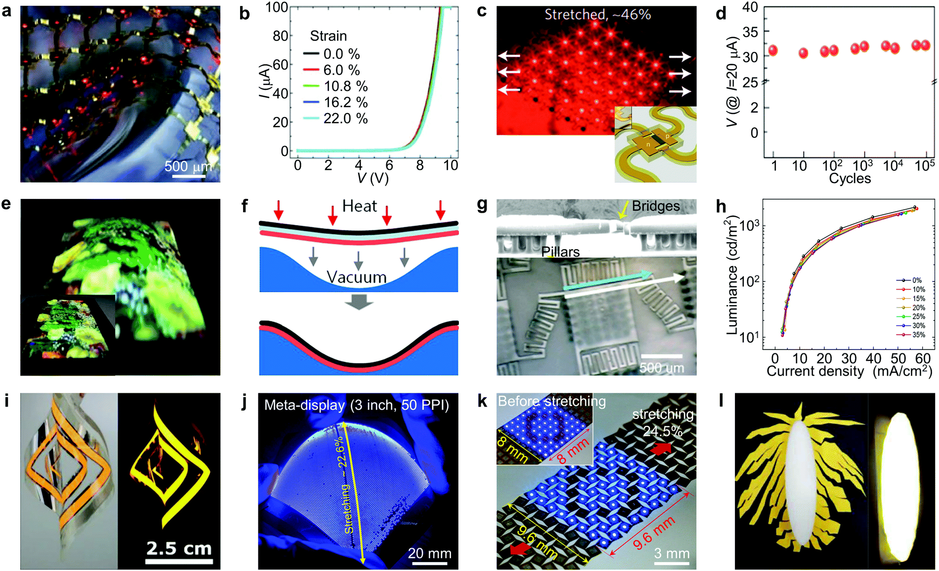
Stretchable ACEL devices have a simple capacitive structure, which consists of a dielectric elastomer layer embedded with luminescent phosphors and two stretchable electrode layers sandwiching the dielectric layer (illustration of an ACEL device in Fig. 1b). Composites of metal-doped zinc sulfide phosphors (dopants: Cu, Mn, Eu, etc.) and elastomers are commonly used as light-emitting layers in stretchable ACEL devices, in which the dopant ions determine the color of the emitted light. With the electrically isolated phosphors in the dielectric layer, the hot-electron impact excitation mechanism is the dominant light emission mechanism of the ACEL devices (Fig. 4a). At high AC voltages (typically >100 V), electrons are injected into phosphors at the interface with elastomer and are accelerated by the electric field. The high kinetic energy of the accelerated electrons causes impact excitation when they meet a luminescent center. Finally, the excited electrons in the luminescent centers generate visible photons. In the opposite electric field, the trapped electrons at the interface between the dielectric and phosphor generate light through the above process in the reverse direction, so an AC voltage is required to circulate the charges within the device. Owing to the capacitive characteristics in the operation mechanism of the ACEL device, its luminance depends on the operating voltage and frequency rather than the current, as shown in eqn (1).109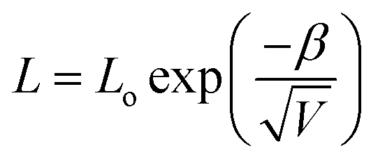 | (1) |
 | ||
| Fig. 4 Intrinsically stretchable ACEL devices. (a) Schematic illustration of the energy diagram and light generation mechanism in ACEL devices. (b) EL intensities of a stretchable ACEL device under different stretching strains. The inset schematic shows the device structure of the stretchable ACEL device. Reproduced with permission from ref. 110. Copyright 2015, Wiley-VCH. (c) Schematic of the morphological and compositional effects of EMIM-TCB on PEDOT:PSS films. Reproduced with permission from ref. 111. Copyright 2017, American Chemical Society. (d) Device structure of a high brightness stretchable ACEL device with high dielectric constant particles, BaTiO3. The inset compares the brightnesses of ACEL devices with (bottom) and without (top) BaTiO3 (250 V, 2.2 kHz). The scale bar is 5 mm. (e) Luminance under 400 Hz square waves as a function of voltage in stretchable ACEL devices with ZnS:Cu–BaTiO3–PDMS (black) and ZnS:Cu–PDMS (red) emissive layers. Reproduced with permission from ref. 112. Copyright 2016, Wiley-VCH. (f) Photographs comparing the brightnesses of P(VDF-HFP) and silicone based ACEL devices in daylight. Reproduced with permission form ref. 113. Copyright 2020, Springer Nature. (g) Photographs of a stretchable ACEL fiber stretched from 0% to 800%. The inset SEM image shows the cross-section of the stretchable ACEL fiber. (h) EL textile containing smile pattern created by weaving stretchable ACEL fibers and commercial wool. Reproduced with permission from ref. 114. Copyright 2018, Wiley-VCH. (i) ACEL speaker operation during finger flexion. Reproduced with permission from ref. 115. Copyright 2021, Wiley-VCH. (j) Sequence of crawling motion by pressurizing the chambers in a multi-functional light-emitting soft robot. Reproduced with permission from ref. 116. Copyright 2016, The American Association for the Advancement of Science (AAAS). (k) Photographs of cut (top) and operation (bottom, after a day) of a self-healable ACEL device. (l) ACEL device operation inside an integrated system with sensors. Heart-shaped pixel blinks when a heartbeat is detected using an ECG sensor (top right). Bar pixels turn on and off based on the values of the heart rate and capacitance detected using the ECG and strain sensors (bottom). Reproduced with permission from ref. 117. Copyright 2018, Springer Nature. | ||
Because of the field induced light generation mechanism with a tens of micrometers thick emissive layer, the surface conductivity and roughness of the conductor are insignificant to the ACEL device operation.118–126 Therefore, most of the stretchable conductors (Ag NWs, CNTs, conductive polymers, etc.) can be used as deformable electrodes in ACEL devices. For example, Wang et al. employed AgNW networks spray-coated on a PDMS substrate as a transparent and stretchable electrode.110 The copper-doped zinc sulfide (ZnS:Cu) microparticle–PDMS precursor mixture was spin-coated and AgNWs were spray-coated for the emission layer and top electrode, respectively (inset of Fig. 4b). The device achieved a brightness of 100 cd m−2 under conditions of 7 V μm−1 at 50 kHz. When the ACEL device was elongated, the brightness increased due to the decrease in the emitter thickness. However, the resistivity of the electrodes was increased, which decreased the brightness of the ACEL devices. Because of these trade-off effects, the brightness of the ACEL device was enhanced in the strain range up to ∼30% but reduced in the larger strain range (Fig. 4b).
In addition to conductive nanomaterials, other types of stretchable electrodes can be adopted to construct ACEL devices. Ionic hydrogels having superior elasticity and transparency can be good candidates for stretchable electrodes.127–130 Meanwhile, the relatively high conductivity and transparency in the visible range make PEDOT:PSS one of the promising conducting polymers for stretchable EL devices.131 Teo et al. reported a highly stretchable and semi-transparent ACEL device using a composite film of PEDOT:PSS-1-ethyl-3-methylimidazolium tetracyanoborate (EMIM-TCB) as transparent electrodes.111 The fibrillar structure of EMIM-TCB and the increased free volume within the polymer chains promoted conductivity and stretchability (Fig. 4c). A mixture of ZnS:Cu and PDMS was used as an emissive layer, and this device exhibited a brightness of 106 cd m−2 withstanding 50% tensile strain under AC bias conditions of 110 V and 1.5 kHz.
Silicone elastomers (i.e., PDMS and Ecoflex) are attractive dielectric matrices for the emissive layer because of their facile mingling with ZnS phosphors.132–134 In ACEL devices, greater electric potentials need to be focused on the phosphors to achieve higher luminance, but silicone elastomer matrices with low dielectric constants (2.3–2.8) decrease the potential concentrated on the phosphors, resulting in a low luminance. To enhance the brightness of a stretchable ACEL device, Stauffer et al. introduced barium titanate (BaTiO3) that features high dielectric permittivity into the phosphor–PDMS composite.112 They fabricated the densely packed emissive layer through sequential filtration of the ZnS:Cu phosphors (∼7 μm) and BaTiO3 particles (∼500 nm) (Fig. 4d). The dielectric constant of the phosphor–BaTiO3–PDMS emissive layer increased by more than twice than that of the phosphor–PDMS emissive layer in all frequency ranges, resulting in a remarkable increase in luminance from 12 cd m−2 to 121 cd m−2 at 250 V with 2.2 kHz operation (Fig. 4e). The device exhibited stable emission during 500 stretching cycles from 20% to 50% strain.
Another approach to enhance the brightness is to use a high dielectric constant elastomer instead of PDMS such as poly((vinylidene fluoride)-hexafluoropropylene) (P(VDF-HFP)).135 The dielectric constant of P(VDF-HFP) is above 10, so the ACEL device with the P(VDF-HFP) based emissive layer can show significantly higher brightness than other polymer based devices.136 Tan et al. introduced a P(VDF-HFP) based high dielectric constant material into emissive layer for a stretchable ACEL device with enhanced brightness and improved operation conditions (lower electric fields, AC voltages, and frequencies).113 A non-ionic fluorosurfactant (FS-300) was added to P(VDF-HFP) to obtain an extremely high dielectric constant (between 10 and 27), which is much higher than those of silicone elastomers (2.5- to 6.8-fold higher). The resulting device demonstrated relatively mild operating conditions of 5 cd m−2 at 50 Hz, 100 V and superior EL properties of 410.6 cd m−2 at 800 Hz, 2 V μm−1 (silicone elastomer-based device: 29.2 cd m−2) (Fig. 4f). Interestingly, the abundant fluorine group inside the fluoroelastomer, P(VDF-HFP), and fluorosurfactant allowed strong hydrogen–fluorine intermolecular bonding, resulting in strong dipole–dipole and van der Waals interactions. Owing to the reversible bonding and low glass transition temperature (−25 °C) of the elastomer matrix, the device also exhibited self-healing properties.
Recently, interest in textile EL devices has emerged for their potential application to wearable displays. They can be fabricated by weaving fiber structured EL devices or interlacing them with traditional yarns or threads. Small openings between neighboring fibers in the textile structure increase stretchability and breathability.137 As a result, textile EL devices are considered as optimal candidates for wearable displays. For fabricating stretchable EL fibers, typically one-dimensional core–shell type EL devices are suggested.138,139 They can be easily manufactured by the sequential coating of the elastomer fiber with a conductive material, a phosphor–PDMS composite, and again with a conductive material. Additionally, super-stretchable EL fibers were constructed by embedding two parallel hydrogel electrodes into the EL layer using the continuous one-step extruding technique (Fig. 4g).114 This EL fiber could be elongated until 800% strain owing to the high stretchability of the conductive hydrogel. Furthermore, the EL fibers were interwoven with the commercial yarn to fabricate an EL textile to display the desired symbols (Fig. 4h).
The simple structure and facile fabrication of ACEL devices allow accessible integration with other devices.140 ACEL devices and dielectric actuating speakers have capacitive architecture; thus, under AC biases, thin ACEL devices could generate audible sound waves through dielectric material vibration (Fig. 4i).115 This sound-in display device generated light-synchronized sound until 150% stretching owing to the strain-insensitive wrinkled AgNW electrode. In another approach, an ACEL device was integrated with soft robots to provide an optical communication ability to the soft robot.116 When pneumatic pressure was applied to the chamber, the crawling robot generated light from its motion according to the capacitance change in each robot panel (Fig. 4j). The Bao group incorporated self-healing polymer into all components of the ACEL device to obtain an EL device with a healing ability; the device could be stretched by ∼50% after the damage recovery (Fig. 4k).117 The ACEL device was integrated with electrocardiogram (ECG) and strain sensors to monitor biomedical signals from a self-healable electronic skin system. The physiological data recorded by each sensor are visualized in real-time, with each pixel of the ACEL array corresponding to heart rate or strain change information (Fig. 4l). This system-level multi-functional self-healable electronic system reinforced the potential of the ACEL device.
As described in this section, the unique characteristics of ACEL devices provide stable light emission and exceptional mechanical properties. However, the huge AC operating voltage (>5 V μm−1) and low luminance (<200 cd m−2) of ACEL devices hinder their wide application in mobile and wearable displays.
3.2 Intrinsically stretchable LECs/LEDs
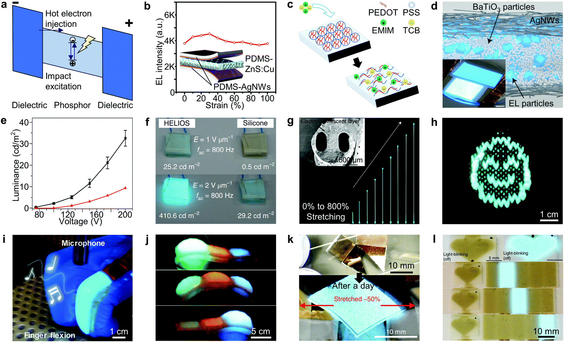
LECs and LEDs have received significant attention due to their high brightness and low operating voltages.141–150 As shown in Fig. 5a, stretchable LECs have a simple device structure, comprising two stretchable electrodes and a stretchable EL layer, including a polymer luminescent layer with ionic conductors and/or solid electrolytes. Under the applied DC bias, n-doping of the EL semiconductor or cation accumulation occurs near the cathode; the opposite happens near the anode, forming a p–i–n junction inside the EL layer. As the charge injection and photon generation arise within the single layer, the EL layer of the LECs is usually thicker than 100 nm. The operating principle of the LEDs was explained in Section 2.1.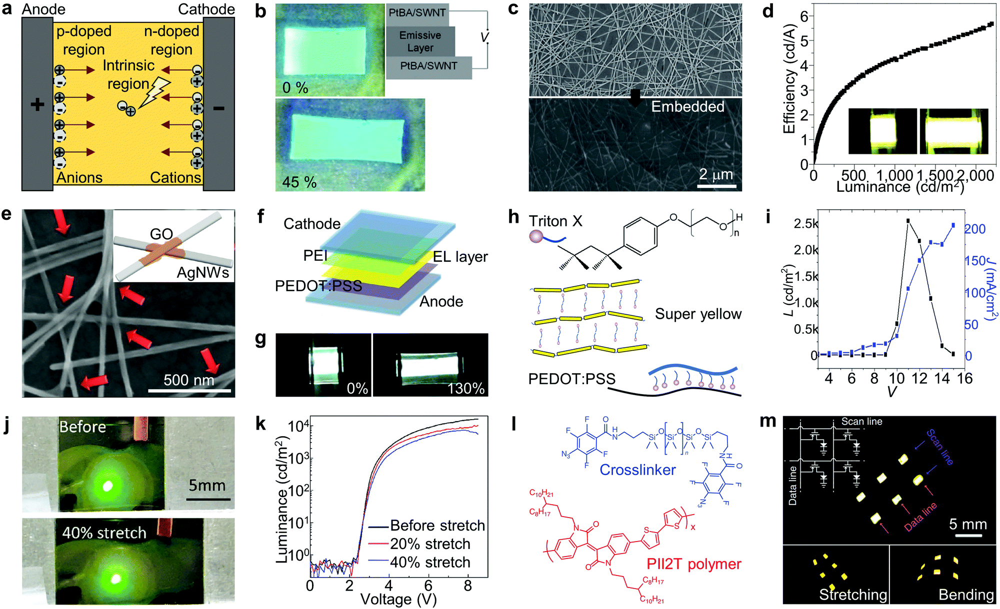 | ||
| Fig. 5 Intrinsically stretchable LECs and LEDs. (a) Schematic illustration of the energy diagram and light generation mechanism in LECs. (b) Emission images of a PLEC at 8 V with different strains (left) and the device structure of the PLEC (right). Reproduced with permission from ref. 151. Copyright 2011, Wiley-VCH. (c) SEM images of AgNW coating on a glass substrate (top) and the surface of an AgNW–PUA composite electrode (bottom). (d) Current efficiency of a stretchable PLEC as a function of luminance. The insets show the stretchable PLEC. Reproduced with permission from ref. 152. Copyright 2013, Springer Nature. (e) SEM image and schematic (inset) of GO-soldered AgNW junctions. (f) Device structure of a fully stretchable PLED. (g) Optical images of a stretchable PLED under specified strains. Reproduced with permission from ref. 153. Copyright 2014, American Chemical Society. (h) Schematics of Triton X (top) and microstructures of Super Yellow and PEDOT:PSS after adding Triton X. (i) J–V–L characteristics of a stretchable OLED. Reproduced with permission from ref. 154. Copyright 2021, The American Association for the Advancement of Science (AAAS). (j) Photographs of a stretchable PeLED under a 4 V bias before (top) and after (bottom) stretching to 40% strain. (k) V–L characteristics of stretchable PeLEDs before and after stretching to 20% and 40% strain. Reproduced with permission from ref. 155. Copyright 2017, Wiley-VCH. (l) Chemical structures of a crosslinker (top) and a PII2T semiconductor polymer (bottom). (m) Images of stretchable AMOLECs. Reproduced with permission from ref. 156. Copyright 2020, Springer Nature. | ||
Due to the nanometer-scale thickness of the light-emitting layer in stretchable LECs and LEDs, the bottom electrode needs to satisfy the ultrahigh flat surface requirement (roughness of a few nanometers or less), which is important to prevent the unwanted device breakdown, as well as the high conductivity for direct charge injection.157,158 The roughness of the conductive nanomaterial network (i.e., carbon nanotube networks or AgNW networks) can be reduced by making the elastomer infiltrate into the percolation network of the nanomaterials. In addition, it is vital to develop intrinsically stretchable semiconductor materials for the emission and charge transport layers with superior optical/electrical/mechanical properties. Therefore, novel intrinsically stretchable semiconducting materials have been synthesized (e.g., EL conjugated polymer) or combinations of various additives are mixed with conventional semiconductor materials to offer them stretchability as well as other required performances.159
To fabricate a stretchable type of composite electrode, the Pei group used a single-walled carbon nanotube (SWNT) network embedded inside a shape-memory polymer, poly(tert-butyl acrylate) (PtBA), which has a low glass transition temperature (∼56 °C).151 Owing to the infiltrated elastomer into the percolated SWNT network,160 the composite electrode showed low surface roughness (<10 nm) and stable sheet resistance after stretching (14% increase of sheet resistance after 14 cycles of 40% strain). The authors constructed a LEC by using a mixture of polyfluorene copolymer (synthesized blue emissive polymer), poly(ethylene oxide) dimethacrylate ether (PEO-DMA) (ionic conductor), and lithium trifluoromethane sulfonate (LiTf) (solid electrolyte), which were sandwiched between two SWNT–PtBA electrodes. The LEC could be turned on at 4.8 V and show a brightness of 200 cd m−2 at 11 V (maximum current efficiency: 1.24 cd A−1). Because of the shape memory properties of the SWNT–PtBA electrodes, the LEC could be stretched up to ∼45% without affecting the EL properties (Fig. 5b).
Similarly, Liang et al. coated a poly(urethane acrylate) (PUA) precursor solution on a percolated AgNW network to achieve a smooth electrode surface (Fig. 5c).152 The resulting electrodes exhibited low sheet resistance (15 Ω sq−1), high stretchability (150%), and low roughness (3.4 nm). A stretchable EL layer was fabricated by mixing the phenyl substituted poly(1,4-phenylene vinylene) (Super Yellow), a crosslinker, a PEO ionic conductor, and LiTf salt. The PEDOT:PSS-coated AgNW–PUA electrode was utilized as a stretchable transparent anode to prevent a potential solvent attack at the EL layer on the PUA substrate. The LEC showed its maximum brightness of 2200 cd m−2 and could be stretched up to 120% (Fig. 5d). The authors also constructed a fully stretchable 5 × 5 array with 1 mm2 pixels by patterning an 80 μm separated AgNW electrode through spray coating.
The operating mechanism of stretchable LECs eliminates the need for the energy band alignment between the electrode and the EL layer. However, the slow turn-on speed and the short lifetime especially at high brightness limit the application of stretchable LECs as commercialized displays.161 On the other hand, LEDs that directly inject charges into the ultrathin EL layer feature high brightness, fast operation, and low operating voltages. To facilitate effective charge injection into the EL layer, multiple charge transport layers with precisely aligned energy band levels are commonly used for LEDs.
AgNWs are one of the most widely utilized metallic fillers for stretchable conductors because of their high aspect ratio and excellent electrical conductivity. During the stretching, however, mechanical failure of the brittle AgNWs and the junctions between the AgNWs results in an increase of the resistance. To solve this problem, the Pei group used a welding technique for the junction of AgNWs with graphene oxide (GO) to decrease the resistance and increase the stability of the percolated network under external strains.153 They employed a white-light-emitting polymer with 1,3-bis[(4-tert-butylphenyl)-1,3,4-oxidiazolyl]phenylene as a stretchable emissive layer and a PUA polymer embedding the graphene oxide (GO)–AgNW network as a stretchable electrode. GO sheets could cover and solder AgNW junctions (Fig. 5e) due to the strong electrostatic force between charged GO and AgNWs and capillary force from the solvent evaporation. This stretchable electrode demonstrated stronger mechanical endurance than heat treated AgNW electrodes. Then, a stretchable PLED was fabricated by employing PEDOT:PSS and polyethylenimine as charge transport layers (Fig. 5f). The resulting LED showed 7 V turn-on voltage, 1100 cd m−2 maximum brightness at 21 V, and 4 cd A−1 maximum current efficiency. Because of the welding of AgNWs by GO, the stretchable electrodes could maintain consistent junction resistance even under elongation of the device, showing light emission from the PLED until 130% applied strain (Fig. 5g).
Recently, Kim et al. added a non-ionic surfactant (Triton-X) to a conjugated polymer (Super Yellow) for a stretchable emissive layer and to PEDOT:PSS for a stretchable HTL.154 Triton-X acted as a plasticizer by reducing the interchain interaction inside Super Yellow and the electrostatic interaction between PEDOT and PSS, increasing the free volume inside the polymer chain network (Fig. 5h). A mixture of doped polyethyleneimine ethoxylated and ZnO nanoparticles was used as an ETL, and AgNWs were used as an electrode. On top of the cathode (AgNWs), interestingly, an additional ETL was coated to facilitate electron injection. The stretchable LED showed a turn-on voltage of 8.3 V, a maximum current efficiency of 1.6 cd A−1, and a maximum brightness of 2500 cd m−2 at 11 V (Fig. 5i). This intrinsically stretchable OLED emitted light at a large applied strain of 80%.
Perovskites are one of the most attractive classes of luminescent materials because of their outstanding color purity (FWHM ∼20 nm) and high photoluminescence quantum yields;162 hence, researchers have attempted to develop stretchable PeLEDs.163,164 Bade et al. introduced PEO into PEDOT:PSS and MAPbBr3 to exploit them as a stretchable anode and a stretchable emissive layer, respectively.155 The PEO-PEDOT:PSS-PDMS electrode and pin-hole-free PEO-MAPbBr3 emissive film endured mechanical deformation up to 50% strain and showed no morphological change. By using eutectic indium–gallium as a cathode, the EL device could be stretched up to 40% (Fig. 5j), exhibiting a turn-on voltage of 2.4 V and a maximum luminance of 15960 cd m−2 at 8.5 V (Fig. 5k).
Integrating intrinsically stretchable TFT and EL arrays can realize a fully stretchable active-matrix-driven display. The Bao group introduced a synthesized azide functionalized PDMS crosslinker to enhance the stretchability of an isoindigo-containing semiconductor (PII2T) and prevent delamination between the perfluorinated elastomer (gate dielectric elastomer) and PII2T (Fig. 5l).156 In conventional NW based stretchable electrodes, the inherent brittleness of NWs limits the entire stretchability, and the empty spaces inside the network may cause inefficient charge injection into the vertically stacked emissive layer. Introduction of conductive polymers into NWs inside the elastomer can be a potential solution to effectively operate stretchable EL devices under stretching conditions. The authors combined conductive PEDOT:PSS with AgNWs–PUA to use them as a stretchable anode. A stretchable PLEC was fabricated by using an AgNW–PUA cathode, a PEDOT:PSS–AgNW–PUA anode, and a stretchable emissive layer composed of Super Yellow, ethoxylated trimethylopropane triacrylate, and LiTf. The stretchable TFT array and the PLEC array were integrated by using an Ag ink, and the 2 × 3 active-matrix PLEC array could withstand various bending deformations as well as 30% stretching (Fig. 5m).
4. Applications of deformable EL devices
Deformable EL devices can be applied to various next-generation electronic systems. This section introduces such system applications of flexible and stretchable EL devices. First, various sensors and deformable EL devices can be combined as integrated systems. In addition, ultrathin EL devices and/or their buckled ones, integrated with wearable photodetectors, can be used for wearable optical health-monitoring devices. Recently, intrinsically stretchable EL devices have also been used to develop intrinsically stretchable wearable systems. Further, flexible EL devices with kirigami/origami designs can be utilized to develop three-dimensionally deformable displays.4.1 Signal output devices for wearable electronic systems
The most representative application of deformable EL devices is a display component in wearable electronic systems.165–168 For example, ultrathin EL devices can be integrated with wearable sensors thanks to their high deformability that enables their conformal contact to the human skin. Song et al. integrated ultrathin skin-mounted QLEDs with wearable and transparent human–machine interfacing (HMI) devices (Fig. 6a).169 In comparison to the ITO electrode, the epoxy–copper–ITO multilayer electrode showed superior conductivity, transparency, and deformability, which could be used for an ultrathin silicon nanomembrane based transparent pressure and touch sensor array (10 × 10). The transparent wearable HMI device was integrated with the QLED and used for the wireless control of a drone.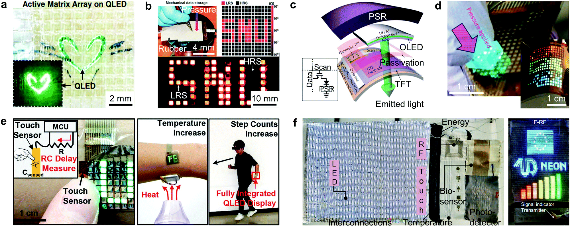 | ||
| Fig. 6 Applications of ultrathin and stretchable EL devices as signal output devices for wearable electronic systems. (a) Optical image of a transparent and multiplexed force touch sensor array (10 × 10) integrated with a QLED laminated on the human skin. The inset shows the QLED under dark conditions. Reproduced with permission from ref. 169. Copyright 2017, Wiley-VCH. (b) The photograph of a MoS2 RRAM array (15 × 15) integrated with pressure sensors and QLEDs. The signals from applied pressure (top left) are stored (top right) and visualized (bottom) using the QLED array. Reproduced with permission from ref. 170. Copyright 2016, Wiley-VCH. (c) Schematic of a user-interactive system integrated with a thin-film transistor, an OLED, and a pressure sensor on a flexible substrate. (d) Image of a 16 × 16 user-interactive AMOLED display showing the local light emission occurring in pressed areas. The inset shows the bendable full-color AMOLED display. Reproduced with permission from ref. 171. Copyright 2013, Springer Nature. (e) Sequential photographs of a passive matrix QLED display integrated with wearable electronics (touch sensor: left, temperature sensor: middle, and step sensor: right) visualizing the data from wearable sensors. Reproduced with permission from ref. 172. Copyright 2017, Wiley-VCH. (f) Photograph of a smart textile display including a 34 inch display and 6 input devices (left). The right photograph exhibits a full-color textile display, which monitors the RF signal strength. Reproduced with permission from ref. 173. Copyright 2022, Springer Nature. | ||
In another example, an ultrathin QLED array was integrated with wearable sensors and actuators to develop a new type of user-interactive system. The ultrathin QLED array was integrated with a pressure sensor and a MoS2 random-access memory (RRAM) array for the user-interactive haptic system (Fig. 6b).170 Mechanical data input from the user was recorded using the pressure sensor and the recorded data were stored in the 15 × 15 RRAM array. The applied external pressure changed the resistance of the piezo-resistive type pressure sensor, and the vertically correlated memory cell stored the mechanical input data by switching its state from the high-resistance state to a low-resistance state. Then the mechanically written data in the memory array were optically visualized with the 15 × 15 QLED array.
Wang et al. reported a flexible user-interactive full-color display that consists of an active-matrix OLED (AMOLED) array and a pressure sensor (Fig. 6c).171 The 16 × 16 AMOLED array was operated with carbon nanotube TFTs and integrated with a pressure sensor made of pressure-sensitive rubber to form an electronic skin. When external pressure was applied, the resistance of the pressure sensor changed and regulated the current through the OLEDs, which changed the brightness of the OLEDs (Fig. 6d). The display brightness was proportional to the applied pressure, and the minimum pressure detection limit was 10 kPa.
Ultrathin wearable displays can be used to visualize various data collected from a series of sensors for wearable electronic systems. For example, Kim et al. developed an ultrathin (∼5.5 μm) passive-matrix (PM) QLED array with a touch user interface (left image of Fig. 6e), which was also integrated with flexible driving circuits and wearable sensors including temperature sensors and accelerometers (right image of Fig. 6e).172 The skin-like display provided real-time visualization of a variety of details to the user, including the user's body temperature and step count information. The user can change the sensing modes between the temperature sensing mode and the step count mode through the touch user interface. The PMQLED array showed minimal temperature rise at high EL brightness (>40000 cd m−2 at 9 V), which is an important prerequisite for the skin-mounted display. Further, no fatigue was observed on the PMQLED array even under extreme mechanical deformations such as wrinkling, curling, and bending.
Conductive fiber-based devices including EL devices can be integrated to develop wearable textile sensors and displays, aiming for IoT applications. Choi et al. reported a 46 inch multifunctional smart textile system which integrated a 34 inch full-color textile display with 6 other types of textile devices, such as a radiofrequency (RF) antenna, a photodetector, a touch sensor, a temperature sensor, a biosensor, and a supercapacitor (left image of Fig. 6f).173 EL fibers were fabricated by mounting red, green, and blue micro LEDs onto copper fibers, which were woven with cotton fibers to fabricate the textile display with a reasonable resolution (2.34 × 10⁴ red, green, and blue subpixels), a low operating voltage (<3 V), and a high luminance (>104 cd m−2). The textile display could visualize various details (e.g., RF signal strength, photodetection, touch, temperature, and ECG signal) from the device components co-integrated in the system (right image of Fig. 6f). In addition, the textile display showed mechanical and electrical reliability even under various mechanical deformations (folding, bending, and rolling). Due to the high flexibility of the Cu fiber (∼2.3 × 10⁶ S m−1 under 10 mm bending conditions), the textile display could maintain the original device performance (ΔJr=10mm = 5 mA cm−2) after 1000 bending cycles.
4.2 Optical input sources for healthcare monitoring
In addition to serving as signal output devices, EL devices can be used as optical input sources. A representative example can be found in healthcare monitoring systems using optical signals.174 For example, pulse oximetry can non-invasively measure the user's oxygen saturation using sensors with a light source and a photodetector (PD). The light emitted from the light source passes through the body part (e.g., fingertip) to the PD, and the change in absorbance can determine the oxygen saturation level. Moreover, this method can be extended to measure a photoplethysmogram (PPG), an optically obtained plenthysmogram showing blood volume changes. PPG sensors can monitor various biomedical signals, including the heart rate, the cardiac cycle, respiration, blood pressures, and hypo- and hyper-volemia. Conventional rigid and large sensors connected to bulky instruments make healthcare monitoring uncomfortable and discontinuous.175 With wearable EL devices, we anticipate that wearable sensors can continuously monitor various biomedical signals without any discomfort.The Someya group integrated flexible PLEDs and organic PDs (OPDs) for an ultrathin (3 μm) reflective pulse oximeter (Fig. 7a).176 Analog and seven-segment digital displays, comprising trichromatic (red, green, and blue) PLEDs, showed the measured data in real-time on the human skin. The high-quality passivation layer, consisting of five alternating inorganic (200 nm-thick SiON) and organic (500 nm-thick parylene) layers, effectively inhibited the diffusion of corrosive media, such as water vapor and oxygen into the device, enabling organic optical devices to operate in air. Due to their ultrathin form factor, the flexible PLEDs, even with brittle ITO electrodes, maintained the device performances under mechanical deformations including bending (bending radius <100 μm) and stretching (1000 cycles with 60% tensile strain). The reflective pulse oximeter with a flexible two-color (red and green) PLED and an OPD was wrapped around the finger to detect pulse waves and blood oxygen levels. The OPD measured variations in the red and green light absorbed by the blood at a driving voltage of 5 V for the PLED. The pulsating PPG signal showed different intensities at different wavelengths due to the differences in the penetration and absorption capacity of hemoglobin (Fig. 7b). The intensity of the PPG signal was consistent with the oxygen saturation. Furthermore, this ultrathin pulse oximeter with passivation layers could continuously monitor for more than 4 days without degeneration in air.
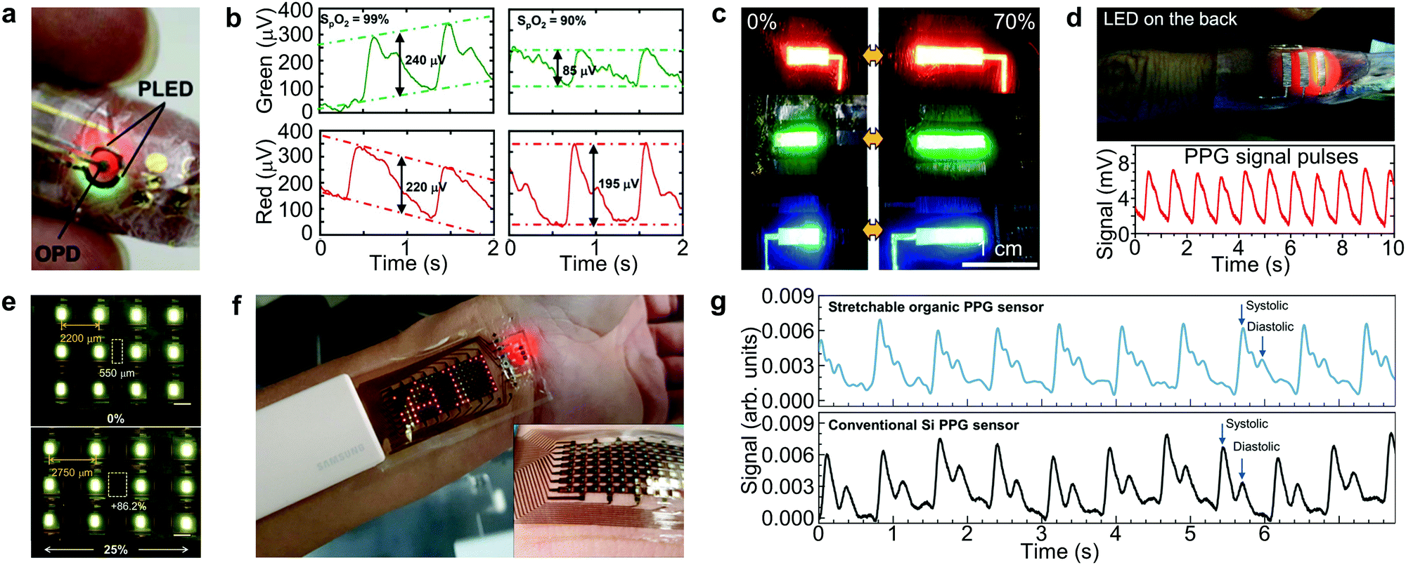 | ||
| Fig. 7 Applications of ultrathin and stretchable EL devices as optical input devices for healthcare monitoring. (a) Photograph of a wearable organic PPG sensor attached on the finger. (b) Output signals from OPDs with different blood oxygenation levels using green (top) and red (bottom) PLEDs. Reproduced with permission from ref. 176. Copyright 2016, The American Association for the Advancement of Science (AAAS). (c) Images of the stretchable red, green, and blue QLEDs at 0% and 70% strains. (d) Photograph of a transmissive PPG sensor composed of QLEDs and QD PDs mounted on a finger (top). The real-time PPG signal pulse from the stretchable QD PD using a red QLED as a light source (bottom). Reproduced with permission from ref. 177. Copyright 2017, American Chemical Society. (e) Microscope images of a stretchable OLED array under strains of 0 and 25%. The OLED pixels were interconnected with intrinsically stretchable electrodes. (f) Photograph of a stretchable organic optoelectronic system including an OLED display and a PPG sensor. The inset shows a conformally attached OLED display on the skin. (g) PPG signals measured using a stretchable organic PPG sensor (top) and a conventional Si PPG sensor (bottom). Reproduced with permission from ref. 178. Copyright 2021, The American Association for the Advancement of Science (AAAS). | ||
Similarly, Kim et al. developed a buckled structure based stretchable transmissive PPG sensor by integrating ultrathin QLEDs and QD PDs on a 70% pre-stretched elastomeric substrate (Fig. 7c).177 The ultrathin QLEDs and QD PDs were fabricated on a 1.3 μm polyethylene naphthalate substrate by using monolayer graphene as transparent electrodes and QDs as emitting and photo-absorbing layers. In the buckled ultrathin optoelectronic device system, the gap between QDs only increased by 0.0004–0.0017 nm under 70% applied strain. This value is much smaller than the length of the organic ligands on the surfaces of the QDs (∼1 nm), which is beneficial for the operation of stretchable devices. Graphene, the thinnest 2D nanomaterial, also provided ultra-high mechanical robustness to pulse oximeters. In addition, the pre-stretched substrate enabled the ultrathin QLED to form a 2D wavy structure that distributed stresses uniformly. The device could tolerate various deformations, including a bending radius of 35 μm and 70% horizontal stretch. The transmissive PPG sensor that consisted of the red QLED and PbS QD PD was attached to the fingertip (top image of Fig. 7d). The red light generated by the QLED penetrated the fingertip and was detected by the epidermal QD PD. The stretchability of the buckled PPG sensor facilitated conformal contact to the fingertip for noise-free measurements with high accuracy and repeatability (bottom image of Fig. 7d). The PPG sensor also performed well under various deformations, such as 70% biaxial stretching, wrinkling, double folding, and 180° twisting.
Stretchable electroluminescent devices can be used as optical input sources as well as signal output devices. Samsung Advanced Institute of Technology developed a stretchable organic optoelectronic system including a PPG sensor (EL device as an optical source) and an OLED array (EL device as a signal output device) to develop a real-time health monitoring patch.178 A micro-cracked Au layer on an elastomer substrate (soft-SEBS), in which Au atoms penetrate into the polymer network during thermal deposition and such penetrated Au atoms enhance the connectivity between micro-cracked Au films, was used as a stretchable interconnect. On the stress relief layer (hard-SEBS) and the deformable micro-cracked Au interconnect, organic layers were deposited for the fabrication of OLEDs (for a PPG sensor and display) and an OPD (for a PPG sensor), followed by thin film encapsulation. The fabricated stretchable OLED array (17 × 7) could be operated well even under various mechanical deformations including crumpling, multi-folding, and twisting, and showed 30% stretchability without notable optical degradation (Fig. 7e). The skin-attachable PPG sensor comprised of an OPD between two red OLEDs could detect volumetric changes of the blood vessel on the wrist. The heart rate signals collected from the PPG sensor were successfully displayed by the stretchable OLED array in real-time (Fig. 7f). The collected signals could be used to analyze the cardiac cycles with systolic and diastolic peaks (Fig. 7g), which could be reliably collected even during the wrist movements owing to the conformal contact and mechanical stability of the stretchable system.
4.3 Intrinsically stretchable displays for wearable systems
Recently, research on intrinsically stretchable EL devices integrated into wearable electronic systems has been actively conducted. For example, the Bao group reported an intrinsically stretchable electrochromic device (ECD) integrated with intrinsically stretchable wireless communication components, which could be operated at a frequency of 13.56 MHz under 50% applied strain.179 For the fabrication of the stretchable ECD, solid electrolyte was sandwiched between stretchable electrodes consisting of PEDOT:PSS with zwitterions. The electrochromic reduction of PEDOT:PSS induced color changes of the ECD at a DC bias of >0.5 V. The stretchable ECD could be operated well under 50% external strain and responded quickly at high frequency (∼10 Hz). For a stretchable wireless system, a stretchable liquid metal antenna and a stretchable resistive strain sensor were integrated to the stretchable ECD (Fig. 8a). In the integrated system, the stretchable ECD could display resistance changes of the strain sensor. The applied strain increased the resistance of the strain sensor, and thus the voltage applied to the ECD was increased. The stretchable ECD could be turned on when the external strain exceeded 10% (Fig. 8b).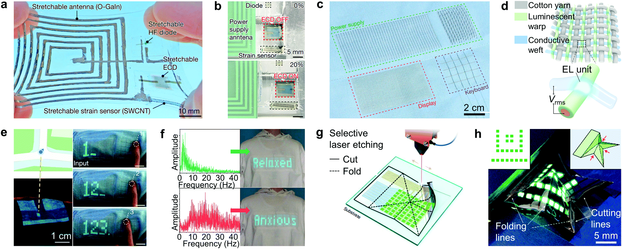 | ||
| Fig. 8 Applications of intrinsically stretchable devices as optical output devices for electronic systems and displays that transform between 2D and 3D architectures. (a) Photograph of an intrinsically stretchable electronic system including an intrinsically stretchable ECD, a strain sensor, and an antenna. (b) Photograph of the stretchable ECD pixels. The ECD turns on at 20% external strain (bottom). Reproduced with permission from ref. 179. Copyright 2021, Springer Nature. (c) Photograph of an integrated textile display including display, keyboard, and power supply modules. (d) Schematic of ACEL textile showing the weave diagram. Each connection between a luminescent warp and a transparent conductive weft forms an EL unit (bottom). (e) Applications of an integrated wearable textile system. The left image shows smart textile navigation and right images show the integrated display and keyboard system (scale bars, 2cm). (f) Expressions of mental states from electroencephalogram signals. The words ‘Relaxed’ (top) and ‘Anxious’ (bottom) are displayed on the textile when the dominant signals are detected in the low-frequency region (0–10 Hz) and the high-frequency region (10–40 Hz), respectively. Reproduced with permission from ref. 180. Copyright 2021, Springer Nature. (g) Schematic of a 3D foldable PM QLED array using selective laser-programmed etching. (h) Photograph of a 3D star-shaped QLED array. The inset shows the pattern (left inset) and structural illustration (right inset) of the QLED array. Reproduced with permission from ref. 181. Copyright 2021, Springer Nature. | ||
Meanwhile, textile displays have attracted attention as next-generation wearable displays. The Peng group reported a self-powered, interactive, and textile wearable system that consisted of a woven ACEL display, a keyboard (information input), and a power supply (combination of an energy harvesting module and an energy storage module) (Fig. 8c).180 The textile display was manufactured by interweaving conductive weft and luminescent warp fibers with micrometer-scale EL elements at the intersected node (Fig. 8d). The transparent ionic weft was produced by melt-spinning of an ion polyurethane gel; Ag-coated nylon thread was then dipped into the ZnS phosphor dispersion to form a luminous warp. Each EL unit showed 115.1 cd m−2 brightness at 2 kHz, 3.7 V μm−1 with less than 8% relative light intensity deviation of 600 EL units. The integrated textile smart display system could detect the user's location through the Bluetooth unit and show the information on the cloth-type display in real time (left images of Fig. 8e). The embedded textile keyboard could be used as a communication platform (right images of Fig. 8e). Furthermore, the textile display showed potential to visually manifest the user's mental state by translating the electroencephalogram signal into perceivable information and showing it on the cloth-type display (Fig. 8f).
4.4 Displays that transform between 2D and 3D architectures
Recently, displays with 3D architecture presenting more realistic images have gained much attention. Therefore, developing displays that can transform between 2D and 3D architectures is highly demanding. Various approaches including origami-/kirigami-based techniques have been applied to fabricating electronic devices that convert 2D to 3D structures.182–185 However, applying these techniques for making displays is challenging because of the complexity of device structures. The Kim group developed a selective laser-programmed etching technique to fabricate an ultrathin (∼13 μm) 3D foldable PM QLED array comprising 64 individual pixels (Fig. 8g).181 The approach could selectively etch the epoxy overcoating layer deposited on the QLED surface without damaging the underlying QLEDs. Using a power-controlled microsecond-pulsed CO2 laser and Ag–Al alloy-type etch-stop layers, it could precisely control the etching depth and the radius of curvature to less than 50 μm. Since the laser-etched part of the device was thinner than the surrounding part, it was easy to get folding lines along which the PM QLED array could be folded like origami (Fig. 8h), achieving free transformation between 2D planar and 3D structures. By carefully designing the structural parameters of PM OLED arrays using mechanical simulations, the strain applied to the luminescent components could be minimized. Even after 500 cycles of repeated folding, the QLEDs, including the folded area, maintain their stable EL performance.5. Conclusions
There have been a large amount of research efforts to advance stretchable EL devices in response to the growing need for high-performance wearable displays. When integrated with other soft electronic device components, deformable EL devices can be utilized as signal output devices (i.e., displays) and/or optical input sources (for optical sensors, together with photodetectors) in the system.We mainly discussed two representative strategies to realize stretchable EL devices: “structural approach by using stretchable device designs” and “material approach by using intrinsically stretchable electronic/optoelectronic materials for device fabrication”. In the first approach, ultrathin flexible EL devices are used as platform devices. To achieve the stretchable form factor, various structural engineering strategies such as buckling/wrinkling, stretchable interconnect designs, and origami/kirigami using folding and cutting have been developed. In the second approach, inherently stretchable electronic/optoelectronic materials have been used for the fabrication of intrinsically stretchable EL devices. ACEL devices and LECs are attractive due to their simple device structures. Stretchable semiconductors (i.e., nanocomposites of organic semiconductors, QDs, and PeNCs) are being researched for intrinsically stretchable LEDs.
Despite these technological advances in stretchable EL devices, many challenges still remain. For example, the buckled/wrinkled structure may cause image distortion depending on the viewing angle. Island–bridge type array designs decrease image resolution due to the large area required for specially designed interconnects. The performance of intrinsically stretchable EL devices (i.e., turn on voltage, luminance, power/quantum efficiency, lifetime, and stability) is significantly behind that of rigid EL devices. For stretchable ACEL devices, further developments of emissive layers are required to lower the operating voltage. For overcoming the slow turn-on characteristics in stretchable LECs, EL materials with increased ion mobility are needed but without any reduction of the device lifetime. The development of novel materials and device designs for intrinsically stretchable LEDs should be made in consideration of the adjacent layers, such as mechanical matching, alignment of energy bands, and solvent effects in the subsequent processing stages.
Recently, there has been meaningful progress in the development of stretchable EL devices, and various applications of ultrathin and stretchable EL devices such as wearable, biomedical, and IoT applications have been demonstrated. Stretchable EL devices can be integrated with other stretchable electronic device components (i.e., sensors, data storage modules, wireless data transport modules, and power supplies) toward fully-integrated wearable electronic systems. Recently highlighted QLEDs and PeLEDs encourage the application of deformable EL devices in wearable and implantable electronic systems owing to their high color purity, low operating voltages, and ultrathin form factors. However, some components in these materials, such as Cd in CdSe QDs or Pb in perovskite materials, are toxic. Heavy-metal free replacements such as InP QDs,11 zinc chalcogenide QDs,186 copper indium chalcogenide QDs,187 and Pb-free perovskite materials188 have been actively investigated, so their application to stretchable EL devices can be another crucial goal for achieving wearable electronic systems.
Conflicts of interest
There are no conflicts to declare.Acknowledgements
This work was supported by IBS-R006-D1, IBS-R006-A1, and the National Research Foundation of Korea (NRF) grants funded by the Korean government (MSIT) (grant no. 2021R1C1C1007997, 2022R1A5A6000846, 2021M3H4A3A01062963, 2021R1C1C1007844, 2021M3I3A1085039). This work was supported by Samsung Research Funding & Incubation Center of Samsung Electronics under project no. SRFC-MA2002-03.Notes and references
- E. H. Kim, S. H. Cho, J. H. Lee, B. Jeong, R. H. Kim, S. Yu, T.-W. Lee, W. Shim and C. Park, Nat. Commun., 2017, 8, 14964 CrossRef CAS PubMed.
- J. H. Koo, S. Jeong, H. J. Shim, D. Son, J. Kim, D. C. Kim, S. Choi, J.-I. Hong and D.-H. Kim, ACS Nano, 2017, 11, 10032–10041 CrossRef CAS PubMed.
- N. Oh, B. H. Kim, S.-Y. Cho, S. Nam, S. P. Rogers, Y. Jiang, J. C. Flanagan, Y. Zhai, J.-H. Kim, J. Lee, Y. J. Yu, Y. K. Cho, G. Hur, J. Zhang, P. Trefonas, J. A. Rogers and M. Shim, Science, 2017, 355, 616–619 CrossRef CAS PubMed.
- J.-K. Song, M. S. Kim, S. Yoo, J. H. Koo and D.-H. Kim, Nano Res., 2021, 14, 2919–2937 CrossRef CAS.
- J. Park, H. Seung, D. C. Kim, M. S. Kim and D.-H. Kim, Adv. Funct. Mater., 2021, 31, 2009281 CrossRef CAS.
- S. Kumar, J. Jagielski, N. Kallikounis, Y.-H. Kim, C. Wolf, F. Jenny, T. Tian, C. J. Hofer, Y.-C. Chiu, W. J. Stark, T.-W. Lee and C.-J. Shih, Nano Lett., 2017, 17, 5277–5284 CrossRef CAS PubMed.
- X. Dai, Y. Deng, X. Peng and Y. Jin, Adv. Mater., 2017, 29, 1607022 CrossRef PubMed.
- L. Kim, P. O. Anikeeva, S. A. Coe-Sullivan, J. S. Steckel, M. G. Bawendi and V. Bulovic, Nano Lett., 2008, 8, 4513–4517 CrossRef CAS PubMed.
- J. Yang, M. K. Choi, D.-H. Kim and T. Hyeon, Adv. Mater., 2016, 28, 1176–1207 CrossRef CAS PubMed.
- H. Cho, S.-H. Jeong, M.-H. Park, Y.-H. Kim, C. Wolf, C.-L. Lee, J. H. Heo, A. Sadhanala, N. Myoung, S. Yoo, S. H. Im, R. H. Friend and T.-W. Lee, Science, 2015, 350, 1222–1225 CrossRef CAS PubMed.
- Y.-H. Won, O. Cho, T. Kim, D.-Y. Chung, T. Kim, H. Chung, H. Jang, J. Lee, D. Kim and E. Jang, Nature, 2019, 575, 634–638 CrossRef CAS PubMed.
- T. Kim, K.-H. Kim, S. Kim, S.-M. Choi, H. Jang, H.-K. Seo, H. Lee, D.-Y. Chung and E. Jang, Nature, 2020, 586, 385–389 CrossRef CAS PubMed.
- V. K. Ravi, S. Saikia, S. Yadav, V. V. Nawale and A. Nag, ACS Energy Lett., 2020, 5, 1794–1796 CrossRef CAS.
- T. Lee, B. J. Kim, H. Lee, D. Hahm, W. K. Bae, J. Lim and J. Kwak, Adv. Mater., 2022, 34, 2106276 CrossRef CAS PubMed.
- C.-Y. Han, S.-H. Lee, S.-W. Song, S.-Y. Yoon, J.-H. Jo, D.-Y. Jo, H.-M. Kim, B.-J. Lee, H.-S. Kim and H. Yang, ACS Energy Lett., 2020, 5, 1568–1576 CrossRef CAS.
- C. R. Kagan, T. Hyeon, D.-H. Kim, R. Ruiz, M. C. Tung and H.-S. P. Wong, MRS Bull., 2020, 45, 807–814 CrossRef.
- J. Yang, J. Yoo, W. S. Yu and M. K. Choi, Macromol. Res., 2021, 29, 391–401 CrossRef CAS.
- B. H. Kim, M. S. Onses, J. B. Lim, S. Nam, N. Oh, H. Kim, K. J. Yu, J. W. Lee, J.-H. Kim, S.-K. Kang, C. H. Lee, J. Lee, J. H. Shin, N. H. Kim, C. Leal, M. Shim and J. A. Rogers, Nano Lett., 2015, 15, 969–973 CrossRef CAS PubMed.
- J. Yang, M. K. Choi, U. J. Yang, S. Y. Kim, Y. S. Kim, J. H. Kim, D.-H. Kim and T. Hyeon, Nano Lett., 2021, 21, 26–33 CrossRef CAS PubMed.
- X. Li, W. Yi, H.-L. Chi, X. Wang and A. P.-C. Chan, Automat. Constr., 2018, 86, 150–162 CrossRef.
- M. Choi, Y. J. Park, B. K. Sharma, S.-R. Bae, S. Y. Kim and J.-H. Ahn, Sci. Adv., 2018, 4, eaas8721 CrossRef PubMed.
- H.-K. Seo, H. Kim, J. Lee, M.-H. Park, S.-H. Jeong, Y.-H. Kim, S.-J. Kwon, T.-H. Han, S. Yoo and T.-W. Lee, Adv. Mater., 2017, 29, 1605587 CrossRef PubMed.
- J. Lim, M. Park, W. K. Bae, D. Lee, S. Lee, C. Lee and K. Char, ACS Nano, 2013, 7, 9019–9026 CrossRef CAS PubMed.
- X. Y. Yang, E. Mutlugun, C. Dang, K. Dev, Y. Gao, S. T. Tan, X. W. Sun and H. V. Demir, ACS Nano, 2014, 8, 8224–8231 CrossRef CAS PubMed.
- D. Kim, Y. Fu, S. Kim, W. Lee, K.-H. Lee, H. K. Chung, H.-J. Lee, H. Yang and H. Chae, ACS Nano, 2017, 11, 1982–1990 CrossRef CAS PubMed.
- Y. Fang, K. Ding, Z. Wu, H. Chen, W. Li, S. Zhao, Y. Zhang, L. Wang, J. Zhou and B. Hu, ACS Nano, 2016, 10, 10023–10030 CrossRef CAS PubMed.
- F. Zhao, D. Chen, S. Chang, H. Huang, K. Tong, C. Xiao, S. Chou, H. Zhong and Q. Pei, J. Mater. Chem. C, 2017, 5, 531–538 RSC.
- X. Chen, J. A. Rogers, S. P. Lacour, W. Hu and D.-H. Kim, Chem. Soc. Rev., 2019, 48, 1431–1433 RSC.
- M. K. Choi, J. Yang, T. Hyeon and D.-H. Kim, npj Flex. Electron., 2018, 2, 10 CrossRef.
- J. H. Koo, D. C. Kim, H. J. Shim, T.-H. Kim and D.-H. Kim, Adv. Funct. Mater., 2018, 28, 1801834 CrossRef.
- M. K. Choi, I. Park, D. C. Kim, E. Joh, O. K. Park, J. Kim, M. Kim, C. Choi, J. Yang, K. W. Cho, J.-H. Hwang, J.-M. Nam, T. Hyeon, J. H. Kim and D.-H. Kim, Adv. Funct. Mater., 2015, 25, 7109–7118 CrossRef CAS.
- Y. J. Song, J.-W. Kim, H.-E. Cho, Y. H. Son, M. H. Lee, J. Lee, K. C. Choi and S.-M. Lee, ACS Nano, 2020, 14, 1133–1140 CrossRef CAS PubMed.
- J. Kim, J. Lee, D. Son, M. K. Choi and D.-H. Kim, Nano Convergence, 2016, 3, 4 CrossRef PubMed.
- S. Kim, J. Byun, S. Choi, D. Kim, T. Kim, S. Chung and Y. Hong, Adv. Mater., 2014, 26, 3094–3099 CrossRef CAS PubMed.
- S. Liu, D. S. Shah and R. Kramer-Bottiglio, Nat. Mater., 2021, 20, 851–858 CrossRef CAS PubMed.
- G. Gustafsson, Y. Cao, G. M. Treacy, F. Klavetter, N. Colaneri and A. J. Heeger, Nature, 1992, 357, 477–479 CrossRef CAS.
- H.-C. Wang, S.-Y. Lin, A.-C. Tang, B. P. Singh, H.-C. Tong, C.-Y. Chen, Y.-C. Lee, T.-L. Tsai and R.-S. Liu, Angew. Chem., Int. Edit., 2016, 55, 7924–7929 CrossRef CAS PubMed.
- T. Q. Trung and N. E. Lee, Adv. Mater., 2017, 29, 1603167 CrossRef PubMed.
- T. Sekitani, H. Nakajima, H. Maeda, T. Fukushima, T. Aida, K. Hata and T. Someya, Nat. Mater., 2009, 8, 494–499 CrossRef CAS PubMed.
- S. H. Chae, W. J. Yu, J. J. Bae, D. L. Duong, D. Perello, H. Y. Jeong, Q. H. Ta, T. H. Ly, Q. A. Vu, M. Yun, X. Duan and Y. H. Lee, Nat. Mater., 2013, 12, 403–409 CrossRef CAS PubMed.
- M. Drack, I. Graz, T. Sekitani, T. Someya, M. Kaltenbrunner and S. Bauer, Adv. Mater., 2015, 27, 34–40 CrossRef CAS PubMed.
- L. Huang, Z. Wang, X. Zhu and L. Chi, Nanoscale Horiz., 2016, 1, 383–393 RSC.
- S. Gong, Y. Wang, L. W. Yap, Y. Ling, Y. Zhao, D. Dong, Q. Shi, Y. Liu, H. Uddin and W. Cheng, Nanoscale Horiz., 2018, 3, 640–647 RSC.
- M. K. Choi, O. K. Park, C. Choi, S. Qiao, R. Ghaffari, J. Kim, D. J. Lee, M. Kim, W. Hyun, S. J. Kim, H. J. Hwang, S.-H. Kwon, T. Hyeon, N. Lu and D.-H. Kim, Adv. Healthcare Mater., 2016, 5, 80–87 CrossRef CAS PubMed.
- E. Roh, B.-U. Hwang, D. Kim, B.-Y. Kim and N.-E. Lee, ACS Nano, 2015, 9, 6252–6261 CrossRef CAS PubMed.
- S. K. Ameri, R. Ho, H. Jang, L. Tao, Y. Wang, L. Wang, D. M. Schnyer, D. Akinwande and N. Lu, ACS Nano, 2017, 11, 7634–7641 CrossRef PubMed.
- J. Yang, M. K. Choi, Y. Sheng, J. Jung, K. Bustillo, T. Chen, S.-W. Lee, P. Ercius, J. H. Kim, J. H. Warner, E. M. Chan and H. Zheng, Nano Lett., 2019, 19, 1788–1795 CrossRef CAS PubMed.
- J. Reeder, M. Kaltenbrunner, T. Ware, D. Arreaga-Salas, A. Avendano-Bolivar, T. Yokota, Y. Inoue, M. Sekino, W. Voit, T. Sekitani and T. Someya, Adv. Mater., 2014, 26, 4967–4973 CrossRef CAS PubMed.
- T.-Y. Wang, J.-L. Meng, Z.-Y. He, L. Chen, H. Zhu, Q.-Q. Sun, S.-J. Ding, P. Zhou and D. W. Zhang, Nanoscale Horiz., 2019, 4, 1293–1301 RSC.
- W. D. Nix, Metall. Trans. A, 1989, 20, 2217–2245 CrossRef.
- M. Kaltenbrunner, M. S. White, E. D. Glowacki, T. Sekitani, T. Someya, N. S. Sariciftci and S. Bauer, Nat. Commun., 2012, 3, 770 CrossRef PubMed.
- S. Choi, H. Lee, R. Ghaffari, T. Hyeon and D.-H. Kim, Adv. Mater., 2016, 28, 4203–4218 CrossRef CAS PubMed.
- S. Wang, J. Song, D.-H. Kim, Y. Huang and J. A. Rogers, Appl. Phys. Lett., 2008, 93, 023126 CrossRef.
- C. Wang, G. Kinzel and T. Altan, J. Mater. Process. Tech., 1993, 39, 279–304 CrossRef.
- M. K. Choi, J. Yang, K. Kang, D. C. Kim, C. Choi, C. Park, S. J. Kim, S. I. Chae, T.-H. Kim, J. H. Kim, T. Hyeon and D.-H. Kim, Nat. Commun., 2015, 6, 7149 CrossRef CAS PubMed.
- M. K. Choi, J. Yang, D. C. Kim, Z. Dai, J. Kim, H. Seung, V. S. Kale, S. J. Sung, C. R. Park, N. Lu, T. Hyeon and D.-H. Kim, Adv. Mater., 2018, 30, 1703279 CrossRef PubMed.
- Y.-F. Li, S.-Y. Chou, P. Huang, C. Xiao, X. Liu, Y. Xie, F. Zhao, Y. Huang, J. Feng, H. Zhong, H.-B. Sun and Q. Pei, Adv. Mater., 2019, 31, 1807516 CrossRef PubMed.
- D. K. Choi, D. H. Kim, C. M. Lee, H. Hafeez, S. Sarker, J. S. Yang, H. J. Chae, G.-W. Jeong, D. H. Choi, T. W. Kim, S. Yoo, J. Song, B. S. Ma, T.-S. Kim, C. H. Kim, H. J. Lee, J. W. Lee, D. Kim, T.-S. Bae, S. M. Yu, Y.-C. Kang, J. Park, K.-H. Kim, M. Sujak, M. Song, C.-S. Kim and S. Y. Ryu, Nat. Commun., 2021, 12, 2864 CrossRef CAS PubMed.
- D. Yin, J. Feng, R. Ma, Y.-F. Liu, Y.-L. Zhang, X.-L. Zhang, Y.-G. Bi, Q.-D. Chen and H.-B. Sun, Nat. Commun., 2016, 7, 11573 CrossRef CAS PubMed.
- T.-H. Kim, K.-S. Cho, E. K. Lee, S. J. Lee, J. Chae, J. W. Kim, D. H. Kim, J.-Y. Kwon, G. Amaratunga, S. Y. Lee, B. L. Choi, Y. Kuk, J. M. Kim and K. Kim, Nat. Photonics, 2011, 5, 176–182 CrossRef CAS.
- C. R. Kagan, C. B. Murray and M. G. Bawendi, Phys. Rev. B, 1996, 54, 8633 CrossRef CAS PubMed.
- C. R. Kagan, C. B. Murray, M. Nirmal and M. G. Bawendi, Phy. Rev. Lett., 1996, 76, 1517 CrossRef CAS PubMed.
- W. K. Bae, J. Lim, D. Lee, M. Park, H. Lee, J. Kwak, K. Char, C. Lee and S. Lee, Adv. Mater., 2014, 26, 6387–6393 CrossRef CAS PubMed.
- T.-H. Kim, D.-Y. Chung, J. Ku, I. Song, S. Sul, D.-H. Kim, K.-S. Cho, B. L. Choi, J. M. Kim, S. Hwang and K. Kim, Nat. Commun., 2013, 4, 2637 CrossRef PubMed.
- J.-S. Park, H. Chae, H. K. Chung and S. I. Lee, Semicond. Sci. Technol., 2011, 26, 034001 CrossRef.
- M. S. White, M. Kaltenbrunner, E. D. Glowacki, K. Gutnichenko, G. Kettlgruber, I. Graz, S. Aazou, C. Ulbricht, D. A.-M. Egbe, M. C. Miron, Z. Major, M. C. Scharber, T. Sekitani, T. Someya, S. Bauer and N. S. Sariciftci, Nat. Photonics, 2013, 7, 811–816 CrossRef CAS.
- M. Choi, S.-R. Bae, L. Hu, A. T. Hoang, S. Y. Kim and J.-H. Ahn, Sci. Adv., 2020, 6, eabb5898 CrossRef CAS PubMed.
- T. Q. Trung, C. Kim, H.-B. Lee, S. M. Cho and N.-E. Lee, Adv. Mater. Technol., 2020, 5, 1900995 CrossRef CAS.
- H.-J. Kwon, J. Hong, H. N. Le, C. Jung, C. E. Park, H. C. Moon, J. Kim and S. H. Kim, Macromol. Res., 2021, 29, 313–320 CrossRef CAS.
- Z. Huang, Z. Tang, J. Yu and S. Bai, Phys. B, 2009, 404, 1790–1793 CrossRef CAS.
- M.-C. Oh, J.-H. Park, H. J. Jeon and J. S. Go, Displays, 2015, 37, 72–78 CrossRef CAS.
- D. Yin, N.-R. Jiang, Z.-Y. Chen, Y.-F. Liu, Y.-G. Bi, X.-L. Zhang, J. Feng and H.-B. Sun, Adv. Opt. Mater., 2020, 8, 1901525 CrossRef CAS.
- D. Yin, N.-R. Jiang, Y.-F. Liu, X.-L. Zhang, A.-W. Li, J. Feng and H.-B. Sun, Light: Sci. Appl., 2018, 7, 35 CrossRef PubMed.
- H. Zhang and J. A. Rogers, Adv. Opt. Mater., 2019, 7, 1800936 CrossRef.
- J. Vanfleteren, I. Chtioui, B. Plovie, Y. Yang, F. Bossuyt, T. Vervust, S. Dunphy and B. Vandecasteele, Proc. Tech., 2014, 15, 208–215 CrossRef.
- T. Kim, H. Lee, W. Jo, T.-S. Kim and S. Yoo, Adv. Mater. Tech., 2020, 5, 2000494 CrossRef CAS.
- A. Carlson, A. M. Bowen, Y. Huang, R. G. Nuzzo and J. A. Rogers, Adv. Mater., 2012, 24, 5284–5318 CrossRef CAS PubMed.
- S.-I. Park, Y. Xiong, R.-H. Kim, P. Elvikis, M. Meitl, D.-H. Kim, J. Wu, J. Yoon, C.-J. Yu, Z. Liu, Y. Huang, K.-C. Hwang, P. Ferreira, X. Li, K. Choquette and J. A. Rogers, Science, 2009, 325, 977–981 CrossRef CAS PubMed.
- R.-H. Kim, D.-H. Kim, J. Xiao, B. H. Kim, S.-I. Park, B. Panilaitis, R. Ghaffari, J. Yao, M. Li, Z. Liu, V. Malyarchuk, D. G. Kim, A.-P. Le, R. G. Nuzzo, D. L. Kaplan, F. G. Omenetto, Y. Huang, Z. Kang and J. A. Rogers, Nat. Mater., 2010, 9, 929–937 CrossRef CAS PubMed.
- J.-H. Hong, J. M. Shin, G. M. Kim, H. Joo, G. S. Park, I. B. Hwang, M. W. Kim, W.-S. Park, H. Y. Chu and S. Kim, J. Soc. Inf. Display, 2017, 25, 194–199 CrossRef CAS.
- M. S. Lim, M. Nam, S. Choi, Y. Jeon, Y. H. Son, S.-M. Lee and K. C. Choi, Nano Lett., 2020, 20, 1526–1535 CrossRef CAS PubMed.
- T. Kim, J. S. Price, A. Grede, S. Lee, G. Choi, W. Guan, T. N. Jackson and N. C. Giebink, Adv. Mater. Technol., 2018, 3, 1800067 CrossRef.
- B. Jang, S. Won, J. Kim, J. Kim, M. Oh, H.-J. Lee and J.-H. Kim, Adv. Funct. Mater., 2022, 32, 2113299 CrossRef CAS.
- Y.-K. Lee, Z. Xi, Y.-J. Lee, Y.-H. Kim, Y. Hao, H. Choi, M.-G. Lee, Y.-C. Joo, C. Kim, J.-M. Lien and I.-S. Choi, Sci. Adv., 2020, 6, eaax6212 CrossRef CAS PubMed.
- R.-H. Kim, M.-H. Bae, D.-G. Kim, H. Y. Cheng, B. H. Kim, D.-H. Kim, M. Li, J. Wu, F. Du, H.-S. Kim, S. Kim, D. Estrada, S. W. Hong, Y. G. Huang, E. Pop and J. A. Rogers, Nano Lett., 2011, 11, 3881–3886 CrossRef CAS PubMed.
- M. S. Kim, G. J. Lee, C. Choi, M. S. Kim, M. Lee, S. Y. Liu, K. W. Cho, H. M. Kim, H. Cho, M. K. Choi, N. Lu, Y. M. Song and D.-H. Kim, Nat. Electronics, 2020, 3, 546–553 CrossRef.
- A. J. Bandodkar, R. Nunez-Flores, W. Jia and J. Wang, Adv. Mater., 2015, 27, 3060–3065 CrossRef CAS PubMed.
- S. Choi, S. I. Han, D. Jung, H. J. Hwang, C. Lim, S. Bae, O. K. Park, C. M. Tschabrunn, M. Lee, S. Y. Bae, J. W. Yu, J. H. Ryu, S.-W. Lee, K. Park, P. M. Kang, W. B. Lee, R. Nezafat, T. Hyeon and D.-H. Kim, Nat. Nanotechnol., 2018, 13, 1048–1056 CrossRef CAS PubMed.
- K. Li, X. Cheng, F. Zhu, L. Li, Z. Xie, H. Luan, Z. Wang, Z. Ji, H. Wang, F. Liu, Y. Xue, C. Jiang, X. Feng, L. Li, J. A. Rogers, Y. Huang and Y. Zhang, Adv. Funct. Mater., 2019, 29, 1806630 CrossRef.
- C. Choi, M. K. Choi, S. Liu, M. S. Kim, O. K. Park, C. Im, J. Kim, X. Qin, G. J. Lee, K. W. Cho, M. Kim, E. Joh, J. Lee, D. Son, S.-H. Kwon, N. L. Jeon, Y. M. Song, N. Lu and D.-H. Kim, Nat. Commun., 2017, 8, 1664 CrossRef PubMed.
- W. Gao, S. Emaminejad, H. Y.-Y. Nyein, S. Challa, K. Chen, A. Peck, H. M. Fahad, H. Ota, H. Shiraki, D. Kiriya, D.-H. Lien, G. A. Brooks, R. W. Davis and A. Javey, Nature, 2016, 529, 509–514 CrossRef CAS PubMed.
- S. Jo, S. Cho, U. J. Yang, G.-S. Hwang, S. Baek, S.-H. Kim, S. H. Heo, J.-Y. Kim, M. K. Choi and J. S. Son, Adv. Mater., 2021, 33, 2100066 CrossRef CAS PubMed.
- S. Jeong, H. Yoon, B. Lee, S. Lee and Y. Hong, Adv. Mater. Technol., 2020, 5, 2000231 CrossRef CAS.
- Y. Wang, C. Zhu, R. Pfattner, H. Yan, L. Jin, S. Chen, F. Molina-Lopez, F. Lissel, J. Liu, N. I. Rabiah, Z. Chen, J. W. Chung, C. Linder, M. F. Toney, B. Murmann and Z. Bao, Sci. Adv., 2017, 3, e1602076 CrossRef PubMed.
- W. Shin, J. S. Kim, H. Kim, H. J. Choi, H. J. Lee, M. K. Um, M. K. Choi and K. Chung, Macromol. Mater. Eng., 2021, 306, 2100007 CrossRef CAS.
- G. D. Cha, W. H. Lee, C. Lim, M. K. Choi and D.-H. Kim, Nanoscale, 2020, 12, 10456–10473 RSC.
- C. Choi, M. K. Choi, T. Hyeon and D.-H. Kim, Chem. Nano. Mat, 2016, 2, 1006–1017 CAS.
- P. Lee, J. Lee, H. Lee, J. Yeo, S. Hong, K. H. Nam, D. Lee, S. S. Lee and S. H. Ko, Adv. Mater., 2012, 24, 3326–3332 CrossRef CAS PubMed.
- F. Xu and Y. Zhu, Adv. Mater., 2012, 24, 5117–5122 CrossRef CAS PubMed.
- M. Zhang, R. Guo, K. Chen, Y. Wang, J. Niu, Y. Guo, Y. Zhang, Z. Yin, K. Xia, B. Zhou, H. Wang, W. He, J. Liu, M. Sitti and Y. Zhang, Proc. Natl. Acad. Sci. U. S. A., 2020, 117, 14667–14675 CrossRef PubMed.
- N. Liu, A. Chortos, T. Lei, L. Jin, T. R. Kim, W.-G. Bae, C. Zhu, S. Wang, R. Pfattner, X. Chen, R. Sinclair and Z. Bao, Sci. Adv., 2017, 3, e1700159 CrossRef PubMed.
- P. Lee, J. Ham, J. Lee, S. Hong, S. Han, Y. D. Suh, S. E. Lee, J. Yeo, S. S. Lee, D. Lee and S. H. Ko, Adv. Funct. Mater., 2014, 24, 5671–5678 CrossRef CAS.
- S. Choi, S. I. Han, D. Kim, T. Hyeon and D.-H. Kim, Chem. Soc. Rev., 2019, 48, 1566–1595 RSC.
- S. Wang, J. Xu, W. Wang, G.-J. N. Wang, R. Rastak, F. Molina-Lopez, J. W. Chung, S. Niu, V. R. Feig, J. Lopez, T. Lei, S.-K. Kwon, Y. Kim, A. M. Foudeh, A. Ehrlich, A. Gasperini, Y. Yun, B. Murmann, J. B.-H. Tok and Z. Bao, Nature, 2018, 555, 83–88 CrossRef CAS PubMed.
- N. Matsuhisa, S. Niu, S. J.-K. O'Neill, J. Kang, Y. Ochiai, T. Katsumata, H.-C. Wu, M. Ashizawa, G.-J. N. Wang, D. Zhong, X. Wang, X. Gong, R. Ning, H. Gong, I. You, Y. Zheng, Z. Zhang, J. B.-H. Tok, X. Chen and Z. Bao, Nature, 2021, 600, 246–252 CrossRef CAS PubMed.
- J. Y. Oh, S. Rondeau-Gagne, Y.-C. Chiu, A. Chortos, F. Lissel, G.-J. N. Wang, B. C. Schroeder, T. Kurosawa, J. Lopez, T. Katsumata, J. Xu, C. Zhu, X. Gu, W.-G. Bae, Y. Kim, L. Jin, J. W. Chung, J. B.-H. Tok and Z. Bao, Nature, 2016, 539, 411–415 CrossRef CAS PubMed.
- H. L. Filiatrault, G. C. Porteous, R. S. Carmichael, G. J.-E. Davidson and T. B. Carmichael, Adv. Mater., 2012, 24, 2673–2678 CrossRef CAS PubMed.
- H. Zhou, J. Park, Y. Lee, J.-M. Park, J.-H. Kim, J. S. Kim, H.-D. Lee, S. H. Jo, X. Cai, L. Li, X. Sheng, H. J. Yun, J.-W. Park, J.-Y. Sun and T.-W. Lee, Adv. Mater., 2020, 32, e2001989 CrossRef PubMed.
- L. Wang, L. Xiao, H. Gu and H. Sun, Adv. Opt. Mater., 2019, 7, 1801154 CrossRef.
- J. Wang, C. Yan, K. J. Chee and P. S. Lee, Adv. Mater., 2015, 27, 2876–2882 CrossRef CAS PubMed.
- M. Y. Teo, N. Kim, S. Kee, B. S. Kim, G. Kim, S. Hong, S. Jung and K. Lee, ACS Appl. Mater. Interfaces, 2017, 9, 819–826 CrossRef CAS PubMed.
- F. Stauffer and K. Tybrandt, Adv. Mater., 2016, 28, 7200–7203 CrossRef CAS PubMed.
- Y. J. Tan, H. Godaba, G. Chen, S. T.-M. Tan, G. Wan, G. Li, P. M. Lee, Y. Cai, S. Li, R. F. Shepherd, J. S. Ho and B. C.-K. Tee, Nat. Mater., 2020, 19, 182–188 CrossRef CAS PubMed.
- Z. Zhang, L. Cui, X. Shi, X. Tian, D. Wang, C. Gu, E. Chen, X. Cheng, Y. Xu, Y. Hu, J. Zhang, L. Zhou, H. H. Fong, P. Ma, G. Jiang, X. Sun, B. Zhang and H. Peng, Adv. Mater., 2018, 30, 1800323 CrossRef PubMed.
- S. Cho, D.-H. Kang, H. Lee, M. P. Kim, S. Kang, R. Shanker and H. Ko, Adv. Sci., 2021, 8, 2001647 CrossRef CAS PubMed.
- C. Larson, B. Peele, S. Li, S. Robinson, M. Totaro, L. Beccai, B. Mazzolai and R. Shepherd, Science, 2016, 351, 1071–1074 CrossRef CAS PubMed.
- D. Son, J. Kang, O. Vardoulis, Y. Kim, N. Matsuhisa, J. Y. Oh, J. W. To, J. Mun, T. Katsumata, Y. Liu, A. F. McGuire, M. Krason, F. Molina-Lopez, J. Ham, U. Kraft, Y. Lee, Y. Yun, J. B.-H. Tok and Z. Bao, Nat. Nanotechol., 2018, 13, 1057–1065 CrossRef CAS PubMed.
- D. Vij, Handbook of electroluminescent materials, CRC Press, 2004 Search PubMed.
- B. You, Y. Kim, B.-K. Ju and J.-W. Kim, ACS Appl. Mater. Interfaces, 2017, 9, 5486–5494 CrossRef CAS PubMed.
- B. S. Kim, H. Kwon, H. J. Kwon, J. B. Pyo, J. Oh, S. Y. Hong, J. H. Park, K. Char, J. S. Ha, J. G. Son and S.-S. Lee, Adv. Funct. Mater., 2020, 30, 1910214 CrossRef CAS.
- H. D. Xuan, B. Timothy, H.-Y. Park, T. N. Lam, D. Kim, Y. Go, J. Kim, Y. Lee, S. I. Ahn, S.-H. Jin and J. Yoon, Adv. Mater., 2021, 33, 2008849 CrossRef PubMed.
- C. Zhao, Y. Zhou, S. Gu, S. Cao, J. Wang, M. Zhang, Y. Wu and D. Kong, ACS Appl. Mater. Interfaces, 2020, 12, 47902–47910 CrossRef CAS PubMed.
- D. Jung, C. Lim, H. J. Shim, Y. Kim, C. Park, J. Jung, S. I. Han, S.-H. Sunwoo, K. W. Cho, G. D. Cha, D. C. Kim, J. H. Koo, J. H. Kim, T. Hyeon and D.-H. Kim, Science, 2021, 373, 1022–1026 CrossRef CAS PubMed.
- H. Joo, D. Jung, S.-H. Sunwoo, J. H. Koo and D.-H. Kim, Small, 2020, 16, 1906270 CrossRef CAS PubMed.
- D. C. Kim, H. J. Shim, W. Lee, J. H. Koo and D.-H. Kim, Adv. Mater., 2019, 32, 1902743 CrossRef PubMed.
- H. J. Shim, S.-H. Sunwoo, Y. Kim, J. H. Koo and D.-H. Kim, Adv. Healthcare Mater., 2021, 10, 2002105 CrossRef CAS PubMed.
- C. H. Yang, B. Chen, J. Zhou, Y. M. Chen and Z. Suo, Adv. Mater., 2016, 28, 4480–4484 CrossRef CAS PubMed.
- J.-Y. Sun, X. Zhao, W. R.-K. Illeperuma, O. Chaudhuri, K. H. Oh, D. J. Mooney, J. J. Vlassak and Z. Suo, Nature, 2012, 489, 133–136 CrossRef CAS PubMed.
- J.-Y. Sun, C. Keplinger, G. M. Whitesides and Z. Suo, Adv. Mater., 2014, 26, 7608–7614 CrossRef CAS PubMed.
- J. Wang, C. Yan, G. Cai, M. Cui, A. L.-S. Eh and P. S. Lee, Adv. Mater., 2016, 28, 4490–4496 CrossRef CAS PubMed.
- S. Kirchmeyer and K. Reuter, J. Mater. Chem., 2005, 15, 2077–2088 RSC.
- L. Cai, S. Zhang, Y. Zhang, J. Li, J. Miao, Q. Wang, Z. Yu and C. Wang, Adv. Mater. Technol., 2018, 3, 1700232 CrossRef.
- S. Song, H. Shim, S. K. Lim and S. M. Jeong, Sci. Rep., 2018, 8, 3331 CrossRef PubMed.
- Y. Zhang, Y. Fang, J. Li, Q. Zhou, Y. Xiao, K. Zhang, B. Luo, J. Zhou and B. Hu, ACS Appl. Mater. Interfaces, 2017, 9, 37493–37500 CrossRef CAS PubMed.
- Y. Zhou, C. Zhao, J. Wang, Y. Li, C. Li, H. Zhu, S. Feng, S. Cao and D. Kong, ACS Mater. Lett., 2019, 1, 511–518 CrossRef CAS.
- Y. Zhou, S. Cao, J. Wang, H. Zhu, J. Wang, S. Yang, X. Wang and D. Kong, ACS Appl. Mater. Interfaces, 2018, 10, 44760–44767 CrossRef CAS PubMed.
- L. Wang, X. Fu, J. He, X. Shi, T. Chen, P. Chen, B. Wang and H. Peng, Adv. Mater., 2020, 32, e1901971 CrossRef PubMed.
- D. Hu, X. Xu, J. Miao, O. Gidron and H. Meng, Materials, 2018, 11, 184 CrossRef PubMed.
- Z. Zhang, X. Shi, H. Lou, X. Cheng, Y. Xu, J. Zhang, Y. Li, L. Wang and H. Peng, J. Mater. Chem. C, 2018, 6, 1328–1333 RSC.
- P. Tan, H. Wang, F. Xiao, X. Lu, W. Shang, X. Deng, H. Song, Z. Xu, J. Cao, T. Gan, B. Wang and X. Zhou, Nat. Commun., 2022, 13, 358 CrossRef CAS PubMed.
- P. Matyba, H. Yamaguchi, M. Chhowalla, N. D. Robinson and L. Edman, ACS Nano, 2011, 5, 574–580 CrossRef CAS PubMed.
- H. Shen, W. Cao, N. T. Shewmon, C. Yang, L. S. Li and J. Xue, Nano Lett., 2015, 15, 1211–1216 CrossRef CAS PubMed.
- H.-H. Chou and C.-H. Cheng, Adv. Mater., 2010, 22, 2468–2471 CrossRef CAS PubMed.
- J. Wu, F. Li, Q. Zeng, C. Nie, P. C. Ooi, T. Guo, G. Shan and Z. Su, Org. Electron., 2016, 28, 314–318 CrossRef CAS.
- J. Fang, P. Matyba and L. Edman, Adv. Funct. Mater., 2009, 19, 2671–2676 CrossRef CAS.
- Y. Shen, H.-Y. Wu, Y.-Q. Li, K.-C. Shen, X. Gao, F. Song and J.-X. Tang, Adv. Funct. Mater., 2021, 31, 2103870 CrossRef CAS.
- Y. Liu, Z. Yu, S. Chen, J. H. Park, E. D. Jung, S. Lee, K. Kang, S.-J. Ko, J. Lim, M. H. Song, B. Xu, H. J. Snaith, S. H. Park and B. R. Lee, Nano Energy, 2021, 80, 105511 CrossRef CAS.
- T. Chiba, Y. Hayashi, H. Ebe, K. Hoshi, J. Sato, S. Sato, Y.-J. Pu, S. Ohisa and J. Kido, Nat. Photonics, 2018, 12, 681–687 CrossRef CAS.
- D. Zhang, Y. Fu, C. Liu, C. Zhao, X. Gao, J. Zhang, W. Guo, J. Liu, C. Qin and L. Wang, Adv. Funct. Mater., 2021, 31, 2103890 CrossRef CAS.
- Y.-H. Kim, S. Kim, A. Kakekhani, J. Park, J. Park, Y.-H. Lee, H. Xu, S. Nagane, R. B. Wexler, D.-H. Kim, S. H. Jo, L. Martinez-Sarti, P. Tan, A. Sadhanala, G.-S. Park, Y.-W. Kim, B. Hu, H. J. Bolink, S. Yoo, R. H. Friend, A. M. Rappe and T.-W. Lee, Nat. Photonics, 2021, 15, 148–155 CrossRef CAS.
- Z. Yu, X. Niu, Z. Liu and Q. Pei, Adv. Mater., 2011, 23, 3989–3994 CrossRef CAS PubMed.
- J. Liang, L. Li, X. Niu, Z. Yu and Q. Pei, Nat. Photonics, 2013, 7, 817–824 CrossRef CAS.
- J. Liang, L. Li, K. Tong, Z. Ren, W. Hu, X. Niu, Y. Chen and Q. Pei, ACS Nano, 2014, 8, 1590–1600 CrossRef CAS PubMed.
- J.-H. Kim and J.-W. Park, Sci. Adv., 2021, 7, eabd9715 CrossRef CAS PubMed.
- S. G.-R. Bade, X. Shan, P. T. Hoang, J. Li, T. Geske, L. Cai, Q. Pei, C. Wang and Z. Yu, Adv. Mater., 2017, 29, 1607053 CrossRef PubMed.
- J. Liu, J. Wang, Z. Zhang, F. Molina-Lopez, G.-J. N. Wang, B. C. Schroeder, X. Yan, Y. Zeng, O. Zhao, H. Tran, T. Lei, Y. Lu, Y.-X. Wang, J. B.-H. Tok, R. Dauskardt, J. W. Chung, Y. Yun and Z. Bao, Nat. Commun., 2020, 11, 3362 CrossRef CAS PubMed.
- R. Ma, S.-Y. Chou, Y. Xie and Q. Pei, Chem. Soc. Rev., 2019, 48, 1741–1786 RSC.
- T.-H. Han, Y. Lee, M.-R. Choi, S.-H. Woo, S.-H. Bae, B. H. Hong, J.-H. Ahn and T.-W. Lee, Nat. Photonics, 2012, 6, 105–110 CrossRef CAS.
- H. Yin, Y. Zhu, K. Youssef, Z. Yu and Q. Pei, Adv. Mater., 2021, 2106184, DOI:10.1002/adma.202106184.
- Y. Zhang, C. J. Sheehan, J. Zhai, G. Zou, H. Luo, J. Xiong, Y. T. Zhu and Q. X. Jia, Adv. Mater., 2010, 22, 3027–3031 CrossRef CAS PubMed.
- K. Schlingman, Y. Chen, R. S. Carmichael and T. B. Carmichael, Adv. Mater., 2021, 33, 2006863 CrossRef CAS PubMed.
- L. Protesescu, S. Yakunin, M. I. Bodnarchuk, F. Krieg, R. Caputo, C. H. Hendon, R. X. Yang, A. Walsh and M. V. Kovalenko, Nano Lett., 2015, 15, 3692–3696 CrossRef CAS PubMed.
- S. Y. Lee, S. Jeon, J. Ahn, J. Bang, H. K. Woo, K.-J. Lee, B. K. Jung, T. Park, D. Son, J.-P. Ahn and S. J. Oh, Appl. Surf. Sci., 2021, 563, 150229 CrossRef CAS.
- D.-H. Jiang, Y.-C. Liao, C.-J. Cho, L. Veeramuthu, F.-C. Liang, T.-C. Wang, C.-C. Chueh, T. Satoh, S.-H. Tung and C.-C. Kuo, ACS Appl. Mater. Interfaces, 2020, 12, 14408–14415 CrossRef CAS PubMed.
- S. Hong, S. Lee and D.-H. Kim, Proc. IEEE, 2019, 107, 2185–2197 CAS.
- Y. Lee, J. Kim, H. Joo, M. S. Raj, R. Ghaffari and D.-H. Kim, Adv. Mater. Technol., 2017, 2, 1700053 CrossRef.
- W. Lee, H. Yun, J.-K. Song, S.-H. Sunwoo and D.-H. Kim, Acc. Mater. Res., 2021, 2, 266–281 CrossRef CAS.
- K. W. Cho, S.-H. Sunwoo, Y. J. Hong, J. H. Koo, J. H. Kim, S. Baik, T. Hyeon and D.-H. Kim, Chem. Rev., 2022, 122, 5068–5143 CrossRef CAS PubMed.
- J.-K. Song, D. Son, J. Kim, Y. J. Yoo, G. J. Lee, L. Wang, M. K. Choi, J. Yang, M. Lee, K. Do, J. H. Koo, N. Lu, J.-H. Kim, T. Hyeon, Y. M. Song and D.-H. Kim, Adv. Funct. Mater., 2017, 27, 1605286 CrossRef.
- D. Son, S. I. Chae, M. Kim, M. K. Choi, J. Yang, K. Park, V. S. Kale, J. H. Koo, C. Choi, M. Lee, J. H. Kim, T. Hyeon and D.-H. Kim, Adv. Mater., 2016, 28, 9326–9332 CrossRef CAS PubMed.
- C. Wang, D. Hwang, Z. Yu, K. Takei, J. Park, T. Chen, B. Ma and A. Javey, Nat. Mater., 2013, 12, 899–904 CrossRef CAS PubMed.
- J. Kim, H. J. Shim, J. Yang, M. K. Choi, D. C. Kim, J. Kim, T. Hyeon and D.-H. Kim, Adv. Mater., 2017, 29, 1700217 CrossRef PubMed.
- H. W. Choi, D.-W. Shin, J. Yang, S. Lee, C. Figueiredo, S. Sionpoli, K. Ullrich, P. Jovančić, A. Marrani, R. Momentè, J. Gomes, R. Branquinho, U. Emanuele, H. Lee, S. Y. Bang, S.-M. Jung, S. D. Han, S. Zhan, W. Harden-Chaters, Y.-H. Suh, X.-B. Fan, T. H. Lee, M. Chowdhury, Y. Choi, S. Nicotera, A. Torchia, F. M. Moncunill, V. G. Candel, N. Durães, K. Chang, S. Cho, C.-H. Kim, M. Lucassen, A. Nejim, D. Jiménez, M. Springer, Y.-W. Lee, S. Cha, J. I. Sohn, R. Igreja, K. Song, P. Barquinha, R. Martins, G. A.-J. Amaratunga, L. G. Occhipinti, M. Chhowalla and J. M. Kim, Nat. Commun., 2022, 13, 814 CrossRef CAS PubMed.
- Y. Lee, J. W. Chung, G. H. Lee, H. Kang, J.-Y. Kim, C. Bae, H. Yoo, S. Jeong, H. Cho, S.-G. Kang, J. Y. Jung, D.-W. Lee, S. Gam, S. G. Hahm, Y. Kuzumoto, S. J. Kim, Z. Bao, Y. Hong, Y. Yun and S. Kin, Sci. Adv., 2021, 7, eabg9180 CrossRef CAS PubMed.
- C. M. Lochner, Y. Khan, A. Pierre and A. C. Arias, Nat. Commun., 2014, 5, 5745 CrossRef CAS PubMed.
- T. Yokota, P. Zalar, M. Kaltenbrunner, H. Jinno, N. Matsuhisa, H. Kitanosako, Y. Tachibana, W. Yukita, M. Koizumi and T. Someya, Sci. Adv., 2016, 2, e1501856 CrossRef PubMed.
- T.-H. Kim, C.-S. Lee, S. Kim, J. Hur, S. Lee, K. W. Shin, Y.-Z. Yoon, M. K. Choi, J. Yang, D.-H. Kim, T. Hyeon, S. Park and S. Hwang, ACS Nano, 2017, 11, 5992–6003 CrossRef CAS PubMed.
- Y. Lee, J. W. Chung, G. H. Lee, H. Kang, J.-Y. Kim, C. Bae, H. Yoo, S. Jeong, H. Cho, S.-G. Kang, J. Y. Jung, D.-W. Lee, S. Gam, S. G. Hahm, Y. Kuzumoto, S. J. Kim, Z. Bao, Y. Hong, Y. Yun and S. Kim, Sci. Adv., 2021, 7, eabg9180 CrossRef CAS PubMed.
- N. Matsuhisa, S. Niu, S. J.-K. O’Neill, J. Kang, Y. Ochiai, T. Katsumata, H.-C. Wu, M. Ashizawa, G.-J. N. Wang, D. Zhong, X. Wang, X. Gong, R. Ning, H. Gong, I. You, Y. Zheng, Z. Zhang, J. B.-H. Tok, X. Chen and Z. Bao, Nature, 2021, 600, 246–252 CrossRef CAS PubMed.
- X. Shi, Y. Zuo, P. Zhai, J. Shen, Y. Yang, Z. Gao, M. Liao, J. Wu, J. Wang, X. Xu, Q. Tong, B. Zhang, B. Wang, X. Sun, L. Zhang, Q. Pei, D. Jin, P. Chen and H. Peng, Nature, 2021, 591, 240–245 CrossRef CAS PubMed.
- D. C. Kim, H. Yun, J. Kim, H. Seung, W. S. Yu, J. H. Koo, J. Yang, J. H. Kim, T. Hyeon and D.-H. Kim, Nat. Electron., 2021, 4, 671–680 CrossRef CAS.
- K. Zhang, Y. H. Jung, S. Mikael, J.-H. Seo, M. Kim, H. Mi, H. Zhou, Z. Xia, W. Zhou, S. Gong and Z. Ma, Nat. Commun., 2017, 8, 1782 CrossRef PubMed.
- H. Fu, K. Nan, W. Bai, W. Huang, K. Bai, L. Lu, C. Zhou, Y. Liu, F. Liu, J. Wang, M. Han, Z. Yan, H. Luan, Y. Zhang, Y. Zhang, J. Zhao, X. Cheng, M. Li, J. W. Lee, Y. Liu, D. Fang, X. Li, Y. Huang, Y. Zhang and J. A. Rogers, Nat. Mater., 2018, 17, 268–276 CrossRef CAS PubMed.
- Z. Yan, F. Zhang, J. Wang, F. Liu, X. Guo, K. Nan, Q. Lin, M. Gao, D. Xiao, Y. Shi, Y. Qiu, H. Luan, J. H. Kim, Y. Wang, H. Luo, M. Han, Y. Huang, Y. Zhang and J. A. Rogers, Adv. Funct. Mater., 2016, 26, 2629–2639 CrossRef CAS PubMed.
- G.-G. Kim, Y. Kim, S. Yoo, H. S. Jang and H. C. Ko, Adv. Mater. Technol., 2020, 5, 2000010 CrossRef CAS.
- J. H. Yu, J. Kim, T. Hyeon and J. Yang, J. Chem. Phys., 2019, 151, 244701 CrossRef PubMed.
- J.-Y. Kim, J. Yang, J. H. Yu, W. Baek, C.-H. Lee, H. J. Son, T. Hyeon and M. J. Ko, ACS Nano, 2015, 9, 11286–11295 CrossRef CAS PubMed.
- X. Li, X. Gao, X. Zhang, X. Shen, M. Lu, J. Wu, Z. Shi, V. L. Colvin, J. Hu, X. Bai, W. W. Yu and Y. Zhang, Adv. Sci., 2021, 8, 2003334 CrossRef CAS PubMed.
Footnote |
| † These authors contributed equally to this work. |
| This journal is © The Royal Society of Chemistry 2022 |