
Printable inks and deformable electronic array devices
Selvaraj
Veerapandian
 a,
Woojo
Kim
b,
Jaehyun
Kim
a,
Youngmin
Jo
b,
Sungjune
Jung
*ab and
Unyong
Jeong
*a
a,
Woojo
Kim
b,
Jaehyun
Kim
a,
Youngmin
Jo
b,
Sungjune
Jung
*ab and
Unyong
Jeong
*a
aDepartment of Materials Science and Engineering, Pohang University of Science and Technology, 77 Cheongam-Ro, Nam-Gu, Pohang 37673, Republic of Korea. E-mail: sjjung@postech.ac.kr; ujeong@postech.ac.kr
bDepartment of Convergence IT Engineering, Pohang University of Science and Technology, 77 Cheongam-Ro, Nam-Gu, Pohang 37673, Republic of Korea
First published on 7th May 2022
Abstract
Deformable printed electronic array devices are expected to revolutionize next-generation electronics. However, although remarkable technological advances in printable inks and deformable electronic array devices have recently been achieved, technical challenges remain to commercialize these technologies. In this review article a brief introduction to printing methods highlighting significant research studies on ink formation for conductors, semiconductors, and insulators is provided, and the structural design and successful printing strategies of deformable electronic array devices are described. Successful device demonstrations are presented in the applications of passive- and active-matrix array devices. Finally, perspectives and technological challenges to be achieved are pointed out to print practically available deformable devices.
 Selvaraj Veerapandian | Veerapandian Selvaraj is a research assistant professor in the Department of Materials and Engineering at the Pohang University of Science and Technology (POSTECH), Korea. Veerapandian Selvaraj obtained his MSc, (2008) and PhD (2016) from the University of Madras, India. His research is focused on the development of deformable conductive materials and fabricating stretchable electronic devices. |
 Woojo Kim | Woojo Kim received the BS degree in electronic engineering from Kyunghee University, Seoul, South Korea, in 2016, where he is currently pursuing the PhD degree under the supervision of Prof. Sungjune Jung in convergence IT engineering. His current research interests include the design and fabrication of flexible printed electronics circuits, memory devices, and systems. |
 Jaehyun Kim | Jaehyun Kim received a BS degree in Materials Science and Engineering from POSTECH in 2018. He is pursuing his PhD degree under the supervision of Prof. Unyong Jeong in the same department. His research interest includes stretchable tactile sensors of E-skin. |
 Youngmin Jo | Youngmin Jo received a BS degree in Mathematics and a MS degree in Interdisciplinary Bioscience and Bioengineering from POSTECH in 2020. He is pursuing his PhD degree under the supervision of Prof. Sungjune Jung in convergence IT engineering. His research interest includes deformable multi-functional sensors. |
 Sungjune Jung | Sungjune Jung is an associate professor at the Department of Materials Science and Engineering and at the Department of Convergence IT Engineering in POSTECH. He received his PhD degree in Manufacturing Engineering from the University of Cambridge in 2007 and subsequently joined the Cavendish Laboratory of the University of Cambridge. Before his PhD, he worked for Samsung Electronics, Digital Printing Division for three years. He has been leading the bio-printing and printed electronics laboratory since he joined POSTECH in 2013. His research focuses on flexible printed electronics and circuits as well as 3D bioprinting and biofabrication. |
 Unyong Jeong | Unyong Jeong is a professor of Materials Science and Engineering at Pohang University of Science and Technology (POSTECH) in Korea and a member of the Korean Academy of Science and Technology. He received a BS degree (1998), MA degree (2000), and PhD degree (2003) in chemical engineering in POSTECH. After working as a postdoctoral fellow at the University of Washing in Seattle, he started his independent research career as an assistant professor in Yonsei University in Korea (2006). He moved to POSTECH (2015) as a Se-Ah distinguished professor. He received Young Scientist Presidential Award (2011), Asian Lecture Award from Japanese chemical society (2013), and Nano Korea Revolutionary Award (Korean Prime Minister award) (2020). He is a member of the Korean Academy of Science and Technology and an associate editor of Journal of Materials Chemistry C. His research includes fabrication of flexible stretchable electronic devices and synthesis of nanostructured materials. |
1. Introduction
Deformable printed electronic devices have attracted immense interest over the past two decades since traditional rigid electronic devices cause mechanical failure when in contact with a soft or nonplanar surface, making deformability (high stability against bending, folding, twisting, and stretching) highly desirable for next-generation electronics.1–4 These new forms of electronic devices are used for interfacing with machines and humans,5–9 for various applications, including electrical circuits,10–18 transistors,19–22 sensors,23–29 and energy storage devices.30,31 Printing is a promising manufacturing technology for the fabrication of electronic components without using expensive processing equipment. Printed electronic devices can be mass-produced over a large area owing to recent developments in printable electrodes,32–34 semiconductors,35–38 and insulators.39,40 Advances in printing techniques38,41–43 facilitated the production of antennas, microelectronic chips, and displays.44–46This article reviews recent developments in deformable printed electronic devices. Since several review articles on deformable printed electronics-, and printing technologies have been published to date,47–49 in this review, we focused on the essential technological elements and fabrication of array-type devices. A brief introduction to printing methods is provided in Section 2, and the design rules for printed array devices are discussed in Section 3. Furthermore, recent applications of printed devices are highlighted in Section 4. Finally, we discuss the technical challenges that must be overcome to realize deformable printed devices in Section 5.
2. Printing methods
Intrinsically deformable inks are processed from a solution composed of a mechanically soft polymer and rigid inorganic materials. Printing methods are classified into contact and noncontact printing.50 Gravure printing and screen printing are examples of contact printing in which the ink is transferred from the surface of patterned structures to the substrate by physical contact. Inkjet printing, nozzle printing, and electrohydrodynamic (EHD) printing are noncontact printing in which the ink is transferred to the substrate via a nozzle or an opening without requiring any printing plate or physical medium carrying the printing information.49–51 The printing method is chosen based on the printed feature size and speed, ink viscosity, surface roughness of the deposited film, and patterning requirements (dimensional resolution, and printing thickness). Typically, low-viscosity inks are printed through inkjet and gravure printing, whereas screen printing, nozzle printing, and EHD printing use high-viscosity inks.2.1 Contact printing
Contact printing typically uses the roll-to-roll process to transfer the ink to the substrate; hence, it is well suited for mass production.52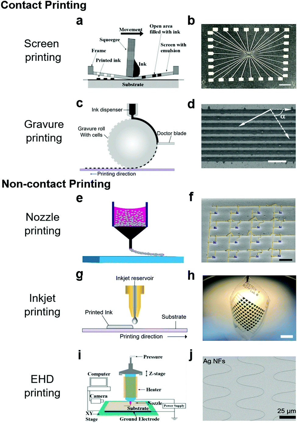 | ||
| Fig. 1 Printing techniques used in printed electronics. (a) Scheme of screen printing. Reproduced and modified with permission.47 Copyright 2021, Wiley-VCH. (b) Digital image of the liquid metal (LM) array printed by screen printing. Scale bar, 5 mm. Reproduced with permission.55 Copyright 2021, Wiley-VCH. (c) Scheme of gravure printing. (d) Optical image of the printed line pattern prepared by gravure printing. Scale bar, 500 μm. Reproduced with permission.57 Copyright 2017, Springer Nature. (e) Scheme of nozzle printing. (f) Colorized SEM image of an LM interconnection array prepared by nozzle printing. The blue and yellow colors correspond to microLED and LM, respectively. Scale bar, 300 μm. Reproduced with permission.60 Copyright 2019, American Association for the Advancement of Science. (g) Scheme of inkjet printing. (h) Digital image of a transistor array fabricated using inkjet printing. Reproduced with permission.64 Copyright 2022, American Chemical Society. (i) Scheme of electrohydrodynamic (EHD) printing. (j) SEM image of Ag nanofibers printed using EHD printing. Reproduced with permission.19 Copyright 2021, American Chemical Society. | ||
2.2 Noncontact printing
Noncontact printing can digitally print various features. It is efficient for on-demand production; however, it allows the printing of only one sample at a time at one printing speed. The printing speed is much slower than that in the case of contact printing.593. Design rules for deformable printed array devices
In this section, we discuss printable functional inks used for flexible and stretchable electronics, addressing methods, and strategies for ensuring the deformability of printed units.3.1. Inks for flexible printed electronic devices
Printable inks of conductors, semiconductors, and dielectrics are necessary to fabricate active electrical components, such as TFTs. Metal and carbon nanomaterials, and conducting polymers have been explored for printable conductive inks. Metal nanomaterials (e.g., metal NPs and nanowires) are particularly promising because they can be dispersed in various solvents. Ag nanomaterials have been extensively printed as electrodes due to their high and reliable electrical conductivity at room temperature.70–74 Grouchko et al. reported an annealing-free conductive ink by adding a destabilizing agent NaCl (Fig. 2a).73 The concept was based on the built-in sintering mechanism. Ag NPs spontaneously self-sintered during the drying step of the printed pattern, eliminating the need for a post-sintering process. Carbon nanomaterials (e.g., graphene and CNTs) are also promising as flexible printed conductors due to their high intrinsic current mobility and mechanical flexibility.75–79 Georgakilas et al. showed a well-dispersed graphene ink with the aid of a hydrophilic functionalized multi-walled CNT stabilizer (Fig. 2b).79 The superstructure exhibited excellent electrical conductivity, making it applicable to high-conductivity ink technologies. Conducting polymers (PEDOT:PSS, polyacetylene, polypyrrole, and polyaniline) have been developed for flexible printable inks due to their light weight, biocompatibility, and refractive index (Fig. 2c).80,81 Compared to metal and carbon-based conductors, the conductivity of conducting polymers is still insufficient for practical electronic applications. Strategies such as treating with solvents or surfactants have been investigated to improve electrical conductivity.82–84 Vosgueritchian et al. incorporated a fluorosurfactant as an additive to create highly conductive and transparent PEDOT:PSS films.83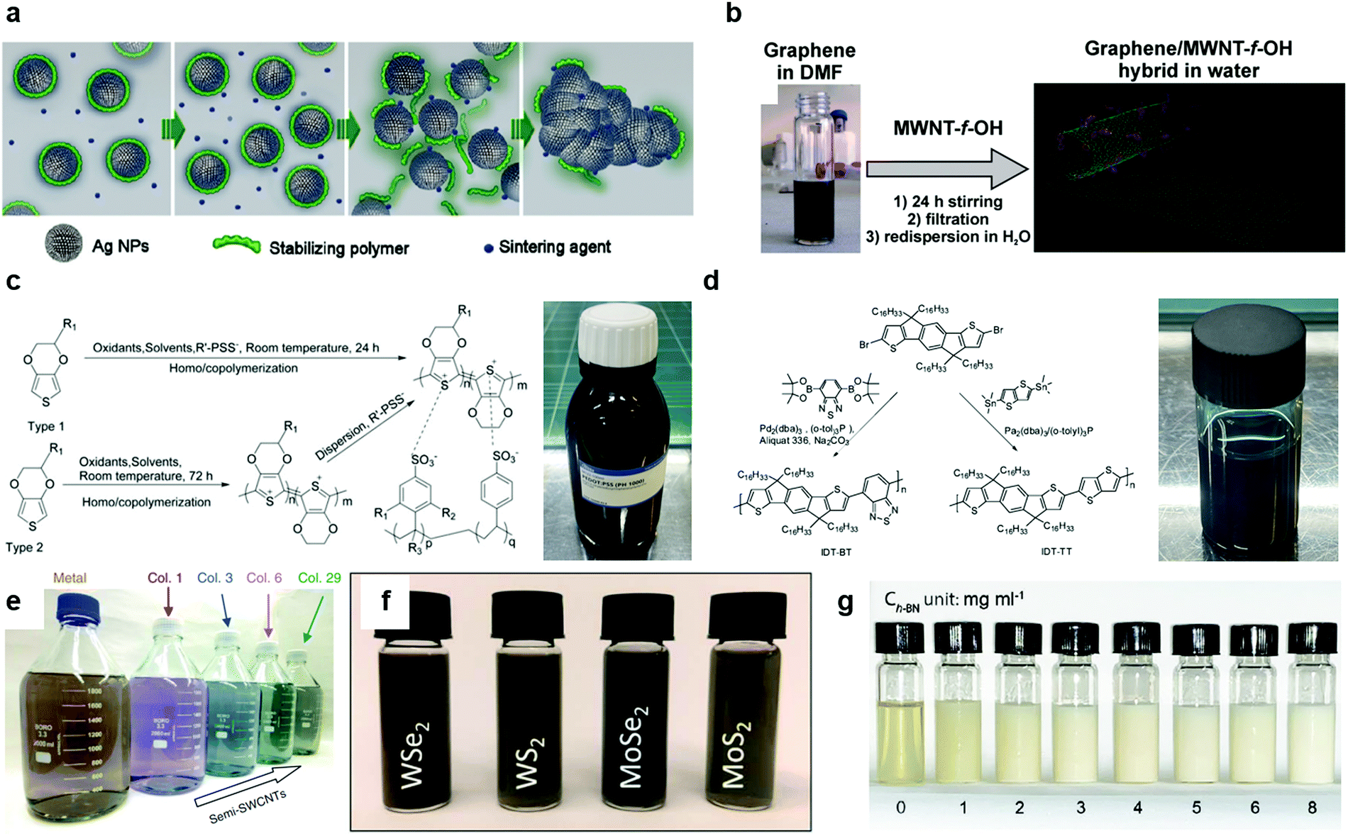 | ||
| Fig. 2 Different types of inks for flexible electronics devices. (a)–(c) Conductive inks based on Ag nanoparticles (a), CNTs (b), and polymers (c). (a) Scheme describing the detachment of the stabilizer from Ag NPs and the self-sintering of the NPs. Reproduced and modified with permission.73 Copyright 2011, American Chemical Society. (b) Formation of the graphene/MWCNT superstructure by hydroxyl functionalized MWCNTs. Reproduced with permission.79 Copyright 2015, Wiley-VCH. (c) Synthetic routes of water-processable PEDOT–PSS, and a commercialized PEDOT–PSS ink by Ossila, Ltd. Reproduced with permission.80 Copyright 2017, Wiley-VCH. (d)–(f) Semiconductor inks based on organic (d), CNT (e), and 2D materials (f). (d) Polymerization and molecular structures of indacenodithiophene copolymers with benzothiadiazole (IDT-BT) and thieno[3,2-b]thiophene (IDT-TT). A stable ink from the polymer. Reproduced with permission.91 Copyright 2010, American Chemical Society. (e) Separation of metallic and semiconducting SWCNTs using the interaction between the chirality of SWCNTs. Reproduced with permission.95 Copyright 2011, Springer Nature. (f) Dispersions of MoS2, MoSe2, WS2, and WSe2 (∼0.2 mg mL−1). Reproduced with permission.104 Copyright 2017, American Association for the Advancement of Science. (g) Dielectric ink consisting of polyurethane (PU) and h-BN nanosheets with different h-BN concentrations (0–8 mg mL−1). Reproduced with permission.125 Copyright 2015, Wiley-VCH. | ||
Various functional semiconducting inks, including organics, CNTs, and 2D materials, have been extensively studied to realize printed electronics.59 For the past decades, organic semiconductors have been the dominating materials as printable functional inks due to their low-temperature processability, excellent compatibility with flexible platforms, and good solubility in low-viscosity organic solvents.85–92 Organic semiconducting materials are generally classified into small molecules and polymers according to their molecular weight. Many efforts have been focused on improving their electrical mobilities. Minemawari et al. considerably improved printed small-molecule organic semiconductors.85 They reported a single crystal layer of 2,7-dioctyl[1]benzothieno[3,2-b][1]benzothiophene (C8-BTBT) using a dual-shot printing method at the liquid–air interface of a nonsolvent with the primary solvent. This printing technique demonstrates a significant step toward large-area flexible printed devices based on high-performance single-crystal semiconductors. Polymer semiconductors are also considered promising printable materials because of their good solubility in solvents and better mechanical flexibility. In 2010, indacenodithiophene copolymers with benzothiadiazole (IDT-BT) and thieno[3,2-b]thiophene (IDT-TT) were reported to provide high-performance air-stable device operation (Fig. 2d).91 Subsequently, Venkateshvaran et al. reported that IDT-BT showed disorder-free transport.92 They confirmed that IDT-BT had a temperature, and gate-voltage independent mobility, and a low Seebeck coefficient. Disorder-free conjugated polymers can achieve high electrical performance regardless of the surface morphologies of printed patterns.
SWCNTs are also promising for flexible electronics due to their processability at low temperatures, remarkable mechanical robustness, and high carrier mobility. Studies performed on SWCNTs involved the separation of metallic and semiconducting CNTs, and the formation of aligned CNT channels and their networks between the source and drain electrodes. The separation of semiconducting SWCNTs was investigated via density gradient ultracentrifugation,93 chromatography,94,95 aqueous two-phase separation,96 and polymer-selective separation.97,98 Liu et al. successfully separated 13 types of single-chiral CNTs from the powder mixture of CNTs grown from high-pressure carbon monoxides (Fig. 2e).95 The sorted CNTs formed well-networked and aligned CNT channels.99–102 The adhesion between CNTs and the substrate plays a vital role in the formation of aligned CNT channels. LeMieux et al. reported that amine-modified substrates provide strengthened adhesion to semiconducting SWCNTs.99 Another approach to forming well-aligned CNTs was achieved using a blade coater.101 Recently, Liu et al. reported multiple dispersion and sorting processes that led to high semiconductor purity and a dimension-limited self-alignment.102
Mechanically flexible and optically transparent 2D materials have emerged as novel materials for fabricating flexible and printed electronics due to their excellent intrinsic mobility in atomically thin channel layers.103–106 Inkjet-printed graphene electronics was first reported using exfoliated graphene ink dispersed in N-methyl-2-pyrrolidone (NMP).103 Recently, transition metal dichalcogenide (TMDC) inks, including WSe2, WS2, MoS2, and MoS2, have also been reported for printed 2D transistors (Fig. 2f).104 Compared to TMDCs fabricated by conventional mechanical exfoliation or chemical vapor deposition, their electrical properties were still inferior; still, they can be used to fabricate printed electronic devices whose performance can be improved further.
Electrical insulating materials with leakage-free dielectric performance and a high capacitance are essential for printed electronic devices such as TFTs and capacitors. Inorganic, organic, and hybrid dielectrics have been extensively studied for printable dielectric inks.107 Inorganic dielectrics (e.g., SiO2, Al2O3, and HfO2) showed high-density and low leakage current. However, printed dielectrics with a low processing temperature have not been widely reported. Vescio et al. demonstrated an inkjet-printed metal–dielectric-metal capacitor on a flexible substrate using an NP-based ink of high-k HfO2.108 Organic dielectrics are highly desirable due to their low-temperature processability and excellent flexibility. Insulating polymers are often used, including poly(methyl methacrylate) (PMMA), poly(4-vinylphenol) (PVP), polystyrene (PS), polyvinyl alcohol (PVA), polyimide (PI), and parylene.88,109–117 Hybrid structures consisting of ion gels, electrolytes, and high-k metal-oxide-embedded polymer dielectrics showed improved dielectric constants and low voltage operation.118–121 Recently, dielectric inks containing 2D h-BN have been developed to achieve excellent printability and high-k dielectrics.122–125 Zhu et al. reported a one-pot coating of a flexible pinhole-free polyurethane (PU)/h-BN composite (Fig. 2g).125
3.2. Inks for stretchable printed electronic devices
Stretchable electronics should be mechanically compliant and electrically stable against repeated substrate deformation. Various printable inks have been explored to obtain functionality (conducting, semiconducting, and dielectric) and ensure stretchability.56 The inks are typically composed of elastomeric polymers (e.g., poly(dimethylsiloxane) (PDMS), polyurethane (PU), and thermoplastic block copolymers (BCP)) and functional nano/micro-sized inorganic materials.126 Adjusting the viscosity and surface energy of the ink significantly affect the printing conditions and the pattern resolution.Metals (e.g., Ag, Au, Cu, Fe, Al, and Ni) have been extensively investigated in stretchable conductive inks, especially Au and Ag due to their relative resistance to oxidation. Conductive metal oxide particles have also been used in conductive inks (Fig. 3a); including zinc oxide (ZnO), aluminum zinc oxide (AZO), gallium zinc oxide (GZO), indium zinc oxide (IZO), indium tin oxide (ITO), antimony oxide (ATO), and fluorine tin oxide (FTO).127 SWCNTs dispersed in a fluorinated rubber,128 and MWCNTs dispersed in a polystyrene-block-poly(ethylene butylene)-block-polystyrene (SEBS) matrix have been widely explored to achieve high stretchability.129 Combining different classes of materials improved both stretchability and conductivity. Gao et al. enhanced the electrical conductivity of graphene fibers by mixing them with commercial Ag nanowires, followed by chemical reduction (Fig. 3b). The Ag-doped graphene fibers possessed a high electrical conductivity of 9.3 × 10⁴ S m−1.130 A CNT ink doped with Ag NPs in an ionic liquid matrix was reported to achieve an electrical conductivity of up to 5710 S cm−1.131 CNT and graphene composite inks were also used to fabricate a stretchable electrode.132
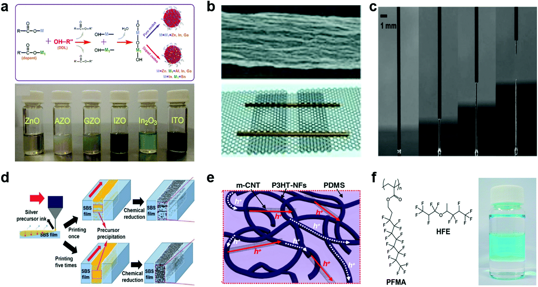 | ||
| Fig. 3 Inks for stretchable printed electronic devices. (a) Synthesis of pure and doped conductive metal oxide NPs (top), and digital image of a series of stable metal oxide NP inks (bottom). Reproduced with permission.127 Copyright 2015, Wiley-VCH. (b) Surface SEM image of the graphene oxide/Ag MW fiber (top), scheme of molecular doping by Ag ions in graphene oxide fibers. Reproduced with permission.130 Copyright 2013, Wiley-VCH. (c) Sequential liquid metal images for use as ink. Reproduced with permission.133 Copyright 2013, Wiley-VCH. (d) Use of metal precursor solution as an ink. A nozzle printing was used to print a Ag precursor ink on a SBS film. The printed precursor was chemically reduced to Ag NPs. Reproduced with permission.145 Copyright 2017, Wiley-VCH. (e) Scheme of the CNT-doped P3HT-NF/PDMS stretchable semiconductor. Reproduced with permission.149 Copyright 2019, American Association for the Advancement of Science. (f) Chemical structures of the semiconductor ink consisting of PFMA and HFE. A vial containing the fluorinated solution (bottom layer), water (middle layer, with blue dye), and an organic layer (top layer). Reproduced with permission.154 Copyright 2013, The Royal Society of Chemistry. | ||
LMs have also been attractive for stretchable electrodes due to their high conductivity and printable fluid properties (Fig. 3c).133 LM alloys such as gallium–indium (EGaIn) and gallium–indium–tin (Galinstan), their elastomer composites, and biphasic conductors are intrinsically stretchable inks. Microfluidics, transfer printing, imprinting, stencil lithography, inkjet printing, and nozzle printing can be used to pattern LMs on soft elastomeric substrates.134–137 These inks provide patterning at the microscale. Their geometries are confined to 2D and 3D structures.133,135,138,139 The printed LM line width of 1.9 μm was achieved by nozzle printing.60 Embedding conductive materials into the surface of a stretchable substrate has also been a promising printing method.140–144 LM–elastomer composites directly printed inside a liquid prepolymer, followed by prepolymer crosslinking, produced a permanent elastomer matrix underneath the substrate surface. Jeong et al. reported a simple strategy in which a metal precursor solution was directly printed on a BCP substrate to allow the precursor to penetrate inside the substrate by chemical binding. Chemical reduction produced metal NPs, electrically percolating inside the substrate (Fig. 3d).145,146 Metallic (1T phase) transition metal dichalcogenides (TMDCs) were used as electrodes for electrochemical systems rather than solid electrical conductors. For instance, exfoliated MoS2 nanosheets homogeneously dispersed in a fluoropolymer elastomer matrix were used as a stretchable solid-state supercapacitor.147
Stretchable semiconducting inks are usually prepared by blending the semiconducting material in an elastomer with the assistance of an appropriate solvent. Semiconducting polymers (mostly polythiophenes (PT)) have been used as p-type materials. Fig. 3e shows self-assembled π-conjugated P3HT NFs blended with CNTs in a PDMS matrix. This composite was uniaxially stretchable up to 100% in repeated stretching cycles and exhibited excellent linearity and no hysteresis.148,149 CNTs and graphene nanomeshes/nanoribbons have also been investigated due to their unique mechanical flexibility.150 Javey et al. reported stretchable SWCNT TFT arrays covering an area of 7.5 cm × 7.5 cm.151 Ceramic oxide NPs (ZnO, SnO2, and Ga2O3, In2O3) and TMDCs were also used as semiconductor materials.38,126,152,153 These materials were mostly mixed with a fluoropolymer for ink preparation. Printed devices constructed with multiple layers require orthogonal inks so that a new printing process does not affect the printed layers. Newby et al. suggested an orthogonal ink that was not mixed with both water and organic solvents (Fig. 3f).154 They dissolved fluorinated polymers in the ink because the polymers prevented the diffusion of water and organic solvent molecules. They demonstrated a printed semiconducting layer on a dielectric layer without affecting the dielectric performance.
Dielectric inks have been rarely investigated compared to conducting or semiconducting inks because polymer-based dielectric materials require a relatively thick layer (>1 μm) to prevent electric leakage. The materials used as substrates (e.g., cellulose, gelatin, shellac, silk, and ceramics) can also be used as dielectrics.155 Polymers such as PMMA, polyimide (PI), polylactic acid (PLA), polyvinyl phenol (PVP), polystyrene (PS), PDMS, polyvinylalcohol (PVA), and benzocyclobutene (BCB), P(VDF-TrFE-CFE), and ion-gel layers have been often used as dielectric materials.118,126,156,157
3.3. Selection of the addressing method
An array device is composed of a plurality of unit elements arranged in a matrix. Addressing is a process where the information to be displayed is converted into sequential voltage pulses to switch active elements or pixels individually, which can be realized using three main methods: direct addressing, passive-matrix addressing, and active-matrix addressing. These techniques are closely related to the types of devices to be driven. An appropriate addressing method is selected based on the overall size, resolution, information content, and input signal frequency.158In direct addressing, individual unit devices have their own electrodes independently controlled by integrated circuits (Fig. 4a). However, the total time for addressing, overall size, and connection complexity considerably increase as the number of unit devices increases; M × N addressing lines are required for M × N electrodes. Matrix addressing is an effective way to alleviate the problems of direct driving. In passive-matrix addressing, active elements are arranged in a matrix form with row and column electrodes (Fig. 4b). Electrodes are patterned into N rows and M columns, resulting in a matrix with M × N addressable intersections, commonly called pixels. The unit device is activated only when its rows and columns are selected. This line-by-line method significantly reduces the number of addressing lines; M + N addressing lines are required for M × N unit devices. However, addressing accuracy cannot be ensured because of the electrical crosstalk between addressing lines.159 This crosstalk causes the generation of unwanted signals from unselected unit devices, which can be problematic for high-density array devices. Active-matrix addressing was proposed for flat panel displays to minimize the crosstalk effect.160 Each unit device is connected to an individual switch in series (Fig. 4c and d). TFTs are generally used as a switch; hence, the device structure becomes complicated, requiring a complex fabrication process. The addressing method must be selected according to the purpose of printed array devices.
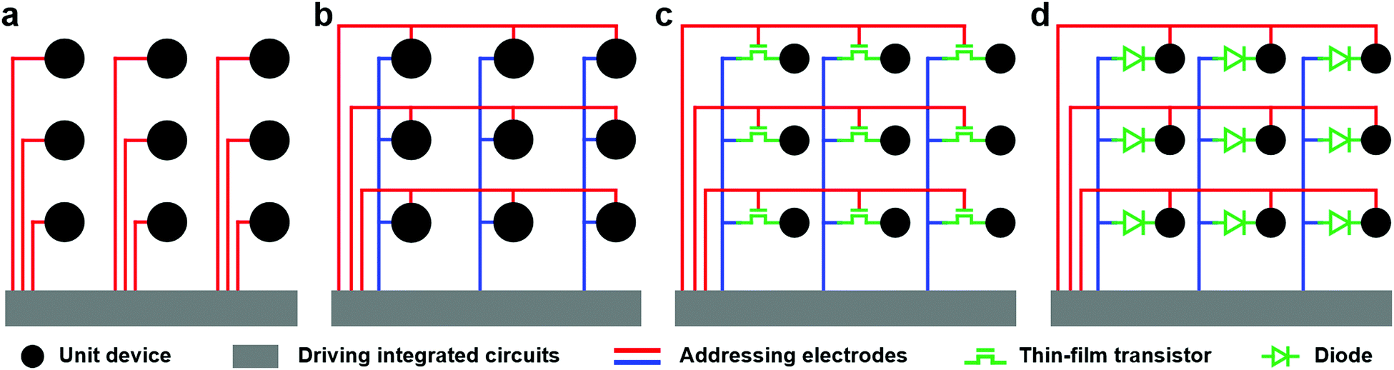 | ||
| Fig. 4 Schematic diagram of data addressing; (a) direct addressing, (b) passive-matrix addressing, (c) active-matrix addressing with thin-film transistors, and (d) active-matrix addressing with diodes. | ||
3.4. Ensuring the deformability of printed units
Studies on achieving stable deformability have targeted the structural design of device components and material design for intrinsic stretchability of printed components. The primary strategy in structural design, which involves in-plane (serpentine) and out-of-plane (buckling) geometries, is to reduce the local strain to preserve conductivity161 and active channel performance.162,163 Serpentine structures are one of the dominant designs used in deformable device architectures. Several printing initiatives have been proposed to realize the controllable production of deformable devices. Fig. 5a illustrates an example of a screen-printed wearable strain sensor array.164 The device comprised free-standing serpentine interconnects prepared by printing a CNT-based ink. The interconnects could accommodate extreme strains up to 500%. The CNT composite in PU offered additional stretchability to the device. Printed micro/nanofibers are advantageous in terms of deformability and spatial resolution. Electrospinning has long been utilized to produce serpentine fibers.165–167 Duan et al. fabricated a microscale serpentine structure by electrospinning straight fibers onto a pre-strained elastomer and then releasing the elastomer (Fig. 5b).168 Fang et al. jet-printed a deformable electrode by making the jet swing back and forth to deposit serpentine fibers on a collector directly.169 Despite significant progress,170 challenges still exist in producing micro/nano serpentine structures with precise wavelength and amplitude. Buckling has been another way to endow deformability in electronic devices. Planar printing of a high modulus pattern has been exploited to induce buckling microstructures.171–173 Lee et al. inkjet-printed silver film patterns on a pre-strained PDMS substrate and demonstrated highly stretchable Ag electrode patterns with negligible resistance changes under repeated stretching cycles (Fig. 5c).174 Typically, cracks are formed in the parallel direction to pre-stretching when the prestrained substrate is released. This crack formation is caused by mismatch of the Poisson ratio between the elastomer substrate and metal films.166,167 The authors effectively suppressed the effect of the Poison ratio mismatch through the in situ annealing process which was based on the fact that the thermal expansion of PDMS can reduce the Poisson's effect.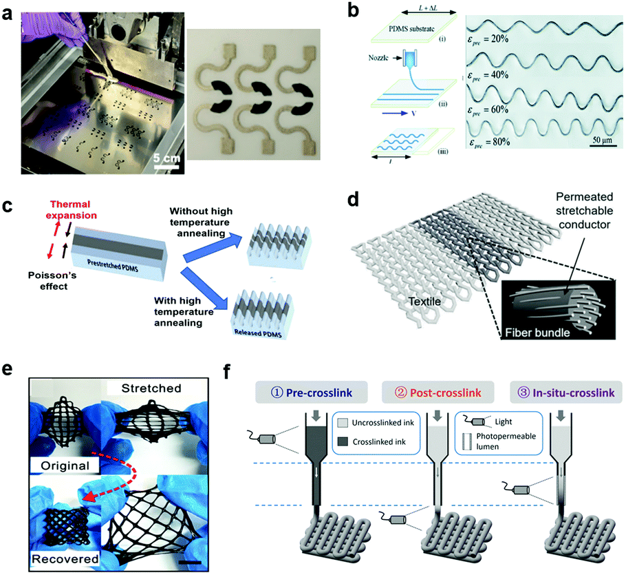 | ||
| Fig. 5 Printing approaches for stretchable electronic devices. (a) Digital image of the stencil employed for screen printing (left). Digital image of a printed CNT-based array device with in-plane curvature (right). Reproduced with permission.164 Copyright 2016, American Chemical Society. (b) Direct writing of straight fibers on a prestrained substrate and releasing of the substrate to produce serpentine fibers (left). OM image of the in-plane curved fibers depending on the prestrain. Reproduced with permission.168 Copyright 2014, The Royal Society of Chemistry. (c) Buckled inkjet-printed silver film on a prestrained PDMS substrate. High temperature annealing prevented crack formation in the transverse direction. Modified with permission.174 Copyright 2013, IOP Publishing. (d) Illustration of the printed stretchable conductive wire prepared on a knit textile. The textile is a permeable composite. Reproduced with permission.178 Copyright 2017, Wiley-VCH. (e) Omnidirectionally-stretchable tough conductive hydrogel mesh produced by nozzle printing. Reproduced with permission.180 Copyright 2021, Springer Nature. (f) Scheme of three different crosslinking strategies with a photo-crosslinkable ink; pre-crosslinking, post-crosslinking, and in situ crosslinking during the printing processes. Reproduced with permission.181 Copyright 2017, Wiley-VCH. | ||
Not only a flat substrate, but a 3D structured substrate can also provide considerable deformability. An electrically percolating network structure with a high degree of porosity is deformable even when the network itself is rigid. Textiles serve as porous substrates for printing, offering comfort, warmth, flexibility, body conformity, and outstanding stretchability.175 Embedding conductive materials inside textile fibers provides a unique advantage of using textiles as stretchable substrates. Even though considerable progress has been made in printed textile electronics,176,177 practical integration into the textile platform has not been realized. Fig. 5d demonstrates an ink-embedded e-textile that could endure 450% elongation through the screen printing of a stretchable Ag ink onto commercially available textiles.178 Compared to the nonembedded inks, the embedded ink delivered significantly lower electrical resistance under the same strain. Choi and co-workers presented the fabrication of a 5 × 7 textile-based microbial fuel cell array by screen-printing PEDOT:PSS as the anode and PEDOT:PSS/silver(I)oxide (Ag2O) as the cathode.179 Although the non-stretchable PEDOT:PSS coating was cracked under stretching, the network remained conductive due to embedded PEDOT:PSS inside the fabric fibers. A porous network with intrinsically stretchable bridges can lead to extreme deformability.
In situ crosslinking of functional inks (while the ink is being printed) can evolve into a new printing technique that can produce a variety of functional materials. Fig. 5e shows a printed tough conductive hydrogel pattern fabricated by orthogonal photochemistry.180 The aqueous monomer (EDOT) was extruded with tyramine-modified PVA, and solidified under visible light irradiation (452 nm) within 30 s. With the freezing treatment, the conductive gel pattern (2 S m−1) was tough but stretchable up to 550%. The methacrylated hyaluronic acid macromer only with 0.05 wt% of photoinitiator could be cured rapidly with visible light exposure at 400–500 nm.181 The ink could be crosslinked in situ during nozzle printing, which enabled pre-crosslinking, post-crosslinking, and in situ crosslinking for the printing process (Fig. 5f). This approach also allowed the printing of heterogeneous and complex structures. The printed filament was uniform and had high cell viability (∼95%). Norbornene-modified hyaluronic acid (NorHA) was also used as a photo-crosslinkable bioink that can be crosslinked via a thiol–ene reaction in the presence of visible light.182
4. Applications
4.1. Flexible printed array devices
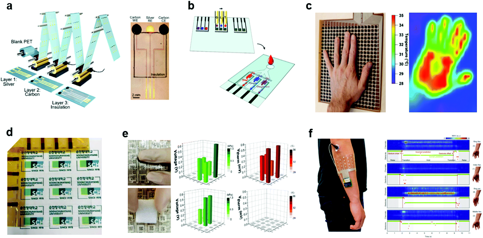 | ||
| Fig. 6 (a) Illustration of the roll-to-roll gravure printing of an electrochemical sensor array on a flexible substrate, and an OM image of the sensor. Reproduced with permission.183 Copyright 2018, American Chemical Society. (b) Illustrative fabrication process of the inkjet-printed multiplexed biosensor for detecting three different metabolites. Reproduced with permission.185 Copyright 2018, American Chemical Society. (c) Photo of a hand placed on the A4-sized temperature sensing mat (left) and the calibrated readout of the temperature profile. Reproduced with permission.188 Copyright 2018, Wiley-VCH. (d) Photo of a transparent printed touch screen sensor. Reproduced with permission.189 Copyright 2020, Wiley-VCH. (e) Demonstration of bimodal sensing of a piezo/thermoelectric tactile sensor array under two different scenarios. Reproduced with permission.190 Copyright 2020, Wiley-VCH. (f) Surface electromyography on the forearm and examples of real-time prediction outputs for four gesture trials. Reproduced with permission.194 Copyright 2020, Springer Nature. | ||
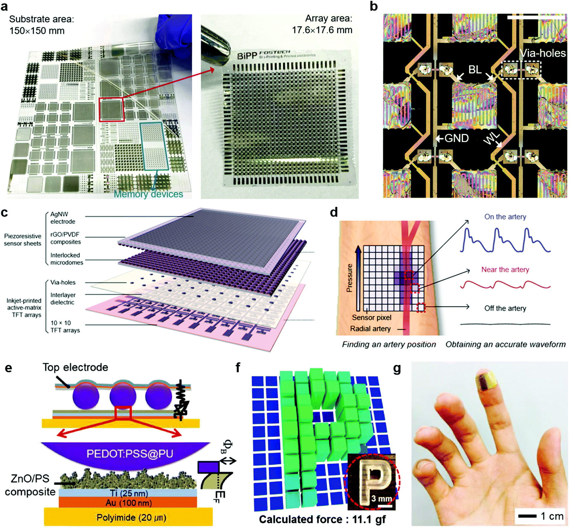 | ||
| Fig. 7 (a and b) Flexible and printed memory array devices. (a) Photographs of large-area memory devices and arrays fabricated by reverse-offset printing. (b) Optical microscopy image of a printed memory array device with WL, BL, GND, and via-holes (scale bar = 500 μm). Reproduced with permission.198 Copyright 2021, Wiley-VCH. (c and d) Design of a wearable active-matrix pressure sensor array. (c) Scheme of a wearable active-matrix pressure sensor array consisting of inkjet-printed active-matrix TFT arrays and piezoresistive sensor sheets. (d) Conceptual diagram of spatiotemporal arterial pulse measurement with a sensor array. The array sensor made it easier to find the artery position and acquire an accurate pulse waveform. Reproduced and modified with permission.64 Copyright 2022, American Chemical Society. (e–g) Flexible e-skin tactile sensor matrix. (e) Scheme of the junction between the PEDOT:PSS-coated microparticle and a ZnO/PS composite layer. The mask pattern was inkjet printed to obtain circular dots of black ink in a square pattern. (f) Current maps of an electronic scale when a P-shaped plastic object was pressed on the sensor with metal bars. (g) Digital image of a flexible tactile array sensor attached to the tip of an index finger as an artificial fingertip. Reproduced with permission.201 Copyright 2021, Wiley-VCH. | ||
Since the reproducible printing of high-density flexible transistors requires sophisticated techniques and know-how, a diode film allowing a one-way current path in sensing pixels can be an efficient strategy. You et al. demonstrated a diode interface by coating a ZnO/PS composite film on a printed Ti/Au electrode.201 They arranged PEODT:PSS-coated conductive PU MPs on the ZnO/PS film (Fig. 7e). The Schottky junction was formed at the interface between the PEDOT:PSS layer and the ZnO/PS film surface, allowing only the current path from ZnO/PS to PEDOT:PSS. This diode approach enabled the high spatial resolution of the pixels (100 pixels cm−2). Since the contact area between the conductive MPs and ZnO/PS layer increased with the increased external pressure, the sensor array provided spatial pressure information without signal interference (Fig. 7f). All the device components were highly flexible, thus they wrapped the finger with the sensor and successfully demonstrated Braille reading (Fig. 7g).
4.2. Stretchable printed array devices
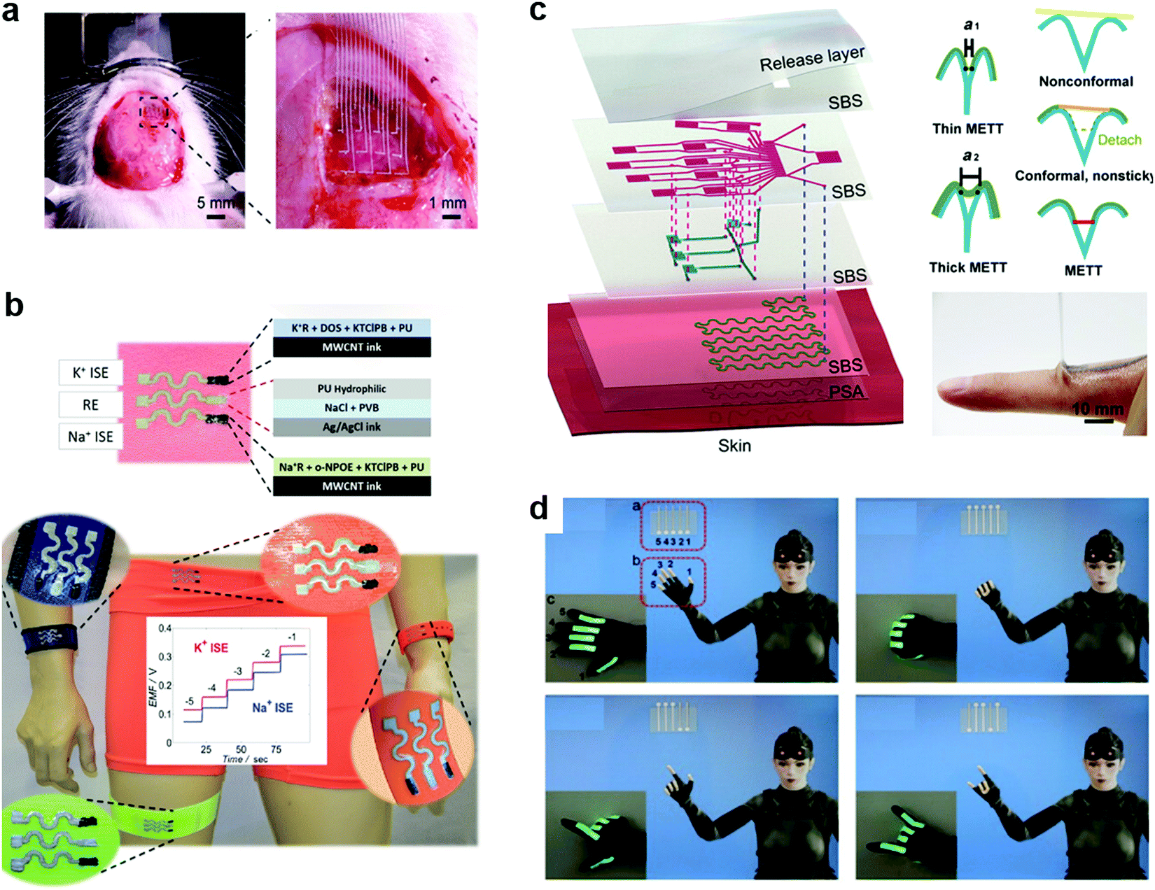 | ||
| Fig. 8 Stretchable passive-type array sensors. (a) Internal surgical images of liquid metal neural electrode arrays showing the high flexibility and conformality of the 16-channel liquid metal electrode on the rat brain. Reproduced with permission.202 Copyright 2021, Wiley-VCH. (b) Tailor-made stretchable materials and the manufacturing process of a wearable sensor based on ion-selective membranes. The sensor can trace the concentration change of potassium and sodium. Reproduced with permission.203 Copyright 2016, Wiley-VCH. (c) Scheme of the multi-layered electronic transfer tattoo (left) and the illustration of surface conformability depending on the substrate thickness and stickiness (right, top). Digital image of peeling off the tattoo from the skin (right, bottom). Reproduced with permission.204 Copyright 2021, American Association for the Advancement of Science. (d) A human–machine interface designed by the Ni–GaIn sensor. Four different hand positions were detected and reconstructed using a computer. Reproduced with permission.205 Copyright 2018, IEEE. | ||
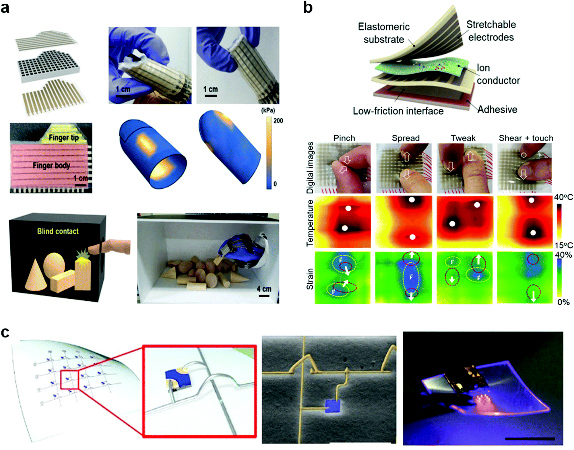 | ||
| Fig. 9 Stretchable active-type arrays. (a) Demonstration of omnidirectional tactility (left, top) and blind contact recognition (left, bottom). Scheme and photo of a customized omnidirectional tactile sensor array wrapped around a finger except the nail (right). The 3D pressure distribution is demonstrated when two points were pressed simultaneously. Reproduced with permission.207 Copyright 2021, Wiley-VCH. (b) Structure of the ion-electronic skin. A pixelated matrix of artificial multimodal ionic receptors is placed on a low-friction layer, and the edges adhere to the elastomer substrate (top). Camera images of the ion-electronic skin under simulations involving multiple stresses (pinch, spread, tweak, shear and touch). The corresponding temperature and strain profiles are shown together (bottom). Reproduced with permission.208 Copyright 2021, American Association for the Advancement of Science. (c) MicroLED array with 3D liquid metal interconnects (left, middle). Photographs of light emission of the microLED array under mechanical bending (right). Reproduced with permission.60 Copyright 2019, American Association for the Advancement of Science. | ||
Operating the device with a switch can remove the electrical crosstalk and make possible the data output expression. Using a stretchable diode can be an effective way to reduce the electrical crosstalk. Bao et al. fabricated intrinsically stretchable diodes consisting of current collector electrodes (Ag NW composites), interface layers (Ag and Au thin films), stretchable cathodes and anodes (PEDOT:PSS with additives), and a stretchable polymer semiconducting layer (Fig. 10a).209 The diode could be stretched up to 50% strain and operated at a high frequency (13.56 MHz), which is sufficient for the wireless operation of soft sensors and electrochromic displays (ECDs) (Fig. 10b).
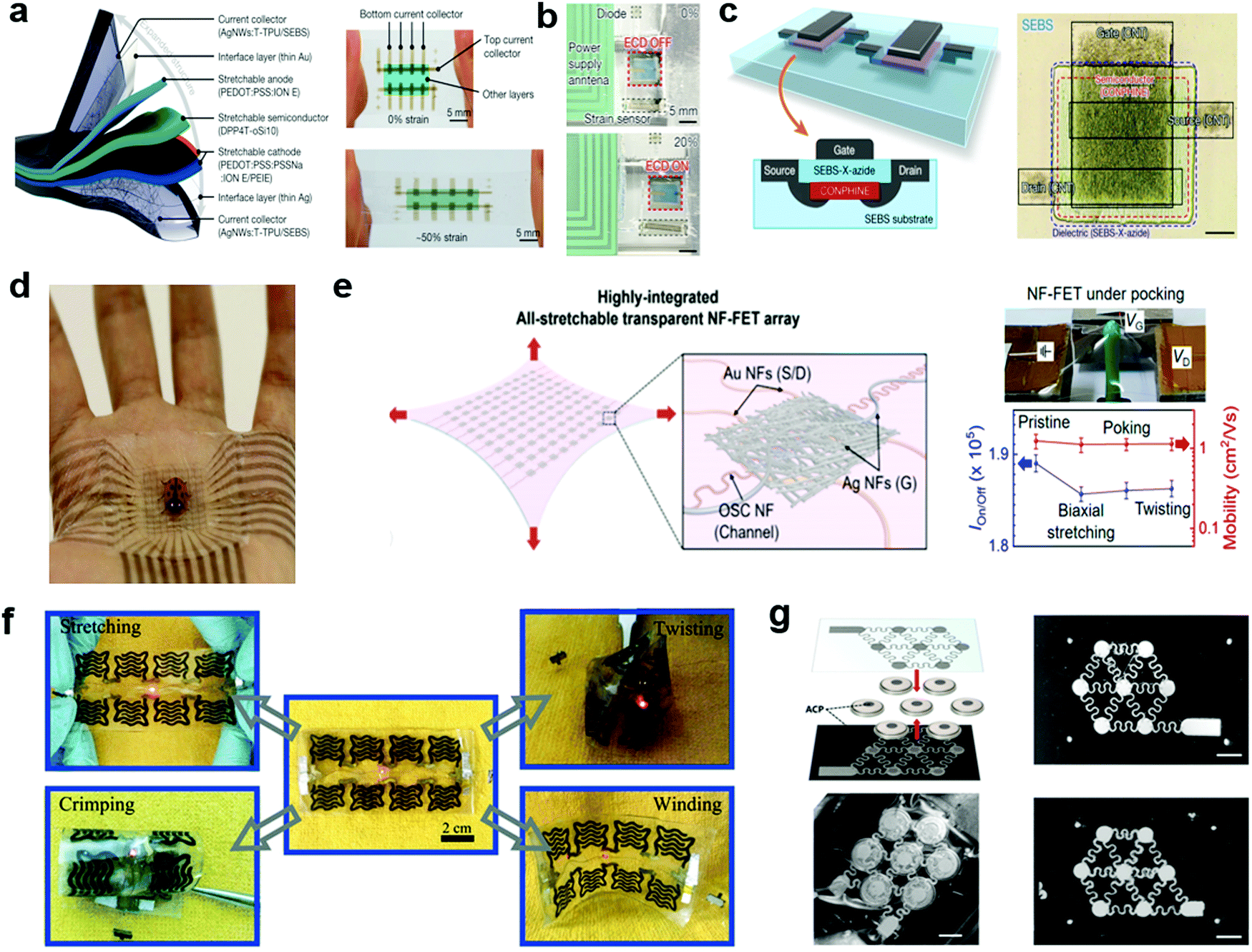 | ||
| Fig. 10 Application of deformable electronic devices. (a) Scheme of an intrinsically stretchable diode consisting of multiple layers (left). Photo of the diode at unstretched and stretched states (50% strain) (right). (b) An electrochromic display that started to turn on after more than 20% strain was applied. Reproduced with permission.209 Copyright 2020, Springer Nature. (c) Schematic illustration (left) and magnified image (right) of an intrinsically stretchable printed polymer transistor array. (d) Photograph of an array that adheres and conforms to a human palm, enabling accurate sensing of the position of a synthetic ladybug with six conductive legs. Reproduced with permission.211 Copyright 2020, Springer Nature. (e) Scheme of a highly integrated all-stretchable transparent array of a nanofiber-field effect transistor (NF-FET) (left). The transistor array was highly deformable without damage under poking (right, top). The stable on/off ratio and mobility of the NF-FET array are shown under various mechanical deformations (right, bottom). Reproduced with permission.19 Copyright 2018, American Chemical Society. (f) Optical images of the stretchable supercapacitor array under stretching, twisting, crimping, and winding with a red LED. Reproduced with permission.214 Copyright 2017, Wiley-VCH. (g) Structural illustration of the printed island-bridge array with Li-ion coin cell batteries. Real image of the assembled stretchable battery pack (left side, bottom). Reproduced with permission.215 Copyright 2018, Wiley-VCH. | ||
Here, the intrinsically stretchable diode was integrated with a stretchable antenna, a strain sensor and ECD pixels. The ECD changes color based on the antenna and diode design. A clear color change was observed when using more than 20% strain. The authors suggested that different types of sensors can be integrated to display the response on the ECD, for example, the ECD can be used with a resistance, pressure and temperature sensor. They used an on-skin wireless stretchable system to display signals from the sensor through display pixels. This process provides a universal platform for the development of next-generation stretchable skin electronic devises.
The fabrication of high-definition stretchable transistors is the eventual direction of incorporating switches. Polymer-based printed stretchable transistors have attracted attention due to their intrinsic flexibility.210 Wang et al. demonstrated a printed stretchable polymer transistor array (Fig. 10c).211 They used a mixture of a semiconducting polymer and BCP elastomer as a stretchable active layer. The semiconducting polymer formed a dense network of nanofibril bundles embedded in the elastomer. They used a crosslinkable SEBS BCP as a stretchable dielectric layer to prevent dissolution by organic solvents. With CNT-based stretchable electrodes, high density organic transistor arrays could be printed. By combining the transistor sets with a piezocapacitive pressure sensor array, a high-resolution stretchable sensitive tactile sensor array was demonstrated (Fig. 10d). To improve the stretchability and transistor performance, intrinsically stretchable semiconductors must be synthesised. Oh et al. demonstrated a stretchable and self-healable semiconducting film, in which the metal coordination bond between the semiconductor and an insulating elastomer was spontaneously reconstructed, which prevented crack formation.212 This dynamic crosslinking approach is a new way of developing multifunctional electronic materials. Kim et al. recently demonstrated an array of stretchable all-nanofiber transparent (∼97%) field-effect transistors. The transistors were statistically reliable and had a hole mobility exceeding 1.0 cm2 V−1 s−1 and an on/off ratio larger than 105. They used EHD printing to directly produce semiconducting polymer nanofibers and source and drain electrodes, and performed electrospinning to produce gate electrodes (Fig. 10e).19 The high-resolution transistor array maintained the transistor performance under repeated cycles of biaxial stretching, poking, and twisting. Compared to organic TFTs, inorganic transistors can offer higher charge mobility and lower operating voltage. Molina-Lopez et al. fabricated an array of transistors by inkjet printing SWCNTs as the active channel and a solid-state ionic PVDF–HFP as the dielectric layer.20 The transistors presented good mobility (27 cm2 V−1 s−1) and an Ion/Ioff ratio (104). Lee et al. fabricated an all-graphene based stretchable and transparent array of FETs on a stretchable rubber substrate using a low-temperature printing process. The transistors showed excellent hole mobility (958 cm2 V−1 s−1) and electron mobility (512 cm2 V−1 s−1).22
Stretchable supercapacitors are essential for energy harvesting and storage systems because of their long cyclic life and high efficiency compared to batteries.213 Interestingly, Shen et al. used nozzle printing to fabricate a stretchable supercapacitor array.214 Supercapacitor arrays were fabricated as an electrode consisting of PANI nanorod-coated MWCNTs to full advantage of both the high specific surface area and excellent conductivity of MWCNTS and the high capacitance of PANI nanorods. It exhibited an aerial capacitance of 44.13 mF cm−2 at an area energy density of 0.004 mW h cm−2. They showed excellent flexibility and stability under stretching, twisting, and crimping (Fig. 10f). Jeong et al. have fabricated stretchable supercapacitors using printable 1T-MoS2 fluoroelastomer ink.148 It can stretch up to 100% strain due to the chemical functionalization of MoS2 with the stretchable fluoroelastomer. It has a specific capacitance of 28 mF cm−2 at a current density of 0.2 mA cm−2 and it retains 80% of its relative capacity (C/C0) at 40% strain.
Interaction between a stretchable power source and a stretchable printed circuit board can be utilized to realize rich potential of stretchable devices. Wang et al. demonstrated a battery array, which was durable under large strain and maintained stable voltage and current output with nearly 100% coulombic efficiency based on screen-printed interconnected arrays.215 This stretchable battery pack included rigid coin-cell LIBs that relied on a printed island-bridge array to accommodate stress-enduring serpentine structures (Fig. 10g). A rigid commercial battery interconnected with uniform, flexible, and stretchable serpentine structures, that can maintain stable voltage and current output is well suited for stretchable battery applications.
5. Technological challenges
Substantial efforts have been devoted to realizing deformable printed array devices via optimizing printed inks, manufacturing processes, and device structures. However, there have been very few examples of practical devices at the commercial level. Technological challenges remain in terms of unit device components;216 printability of interconnection with high spatial-resolution, stability of electrical conductivity and channel mobility under deformation, and deformability of dielectric materials with a large dielectric constant. The most basic device components for securing deformability involve the electrodes and interconnections. Larsen et al. found that the oxide skin of LM can be viscoelastic,217 and Jeong et al. reported that the oxide skin can be highly conductive and viscoplastic.16 A ductile aluminium oxide layer was also observed when it was an amorphous thin film without containing large cracks.218 These viscoplastic oxides allow the preparation of functional metal oxide nanoparticle inks that can be deformable under mechanical stimulation.Printed unit elements are currently operated by rigid chips and power sources. The use of Si-based rigid microchips for deformable devices requires a direct connection between the metal pads of the microchip and the deformable interconnections. This connection is typically achieved using an anisotropic conductive film (ACF) or via holes. Although a stretchable-ACF (S-ACF) has recently been developed for 50 μm interconnetions,219 vertical connections on the order of a few micrometers must be achieved for high-definition devices. Using a rigid power source is another hurdle for deformable devices. Song et al. fabricated a deformable rechargeable thin film battery and used it as a stretchable substrate for device integration.220 This approach enabled the fabrication of stretchable printed circuit boards; however, the power of the battery must be considerably increased for practical uses.
In addition to unit components, large scale production compatible with conventional industrial processes is required. The medium-scale integration of 10–100 printed TFTs has been successfully demonstrated,221 and the printing is now facing increasing demand for large-scale integration, enabling the fabrication of 100–1000 monolithic devices on a flexible substrate. This requires electronic design automation (EDA) tools with process design kits containing parameterized process information (design rules, device models, and so on). However, advanced system design for printing is limited by the lack of EDA approaches. The existing EDA tools of the current CMOS industry have not been employed for printed electronics, and the design rules have been rarely reported because printing processes starkly differ from the conventional photolithography method used for CMOS fabrication. This approach will open up new possibilities for commercializing deformable printed sensors and circuits for internet of everything, wearable healthcare monitoring, smart packaging, and so on where the integration of hundreds of printed devices into a limited deformable sheet are essential requirements.
Conflicts of interest
There are no conflicts to declare.Acknowledgements
This work was supported by the National Research Foundation of Korea (NRF) grant (2021R1A4A1021972) and the Korea Innovation Foundation (INNOPOLIS) grant (2020-DD-UP-0278) funded by the Korea government (MSIT).Notes and references
- J. A. Rogers, T. Someya and Y. Huang, Science, 2010, 327, 1603–1607 CrossRef CAS PubMed.
- W. S. Wong and A. Salleo, 2009, p. 474.
- A. C. Arias, J. D. MacKenzie, I. McCulloch, J. Rivnay and A. Salleo, Chem. Rev., 2010, 110, 3–24 CrossRef CAS PubMed.
- M. L. Hammock, A. Chortos, B. C.-K. Tee, J. B.-H. Tok and Z. Bao, Adv. Mater., 2013, 25, 5997–6038 CrossRef CAS PubMed.
- T. R. Ray, J. Choi, A. J. Bandodkar, S. Krishnan, P. Gutruf, L. Tian, R. Ghaffari and J. A. Rogers, Chem. Rev., 2019, 119, 5461–5533 CrossRef CAS PubMed.
- H. Xu, L. Yin, C. Liu, X. Sheng and N. Zhao, Adv. Mater., 2018, 30, 1800156 CrossRef PubMed.
- Y. Khan, A. E. Ostfeld, C. M. Lochner, A. Pierre and A. C. Arias, Adv. Mater., 2016, 28, 4373–4395 CrossRef CAS PubMed.
- S. Choi, H. Lee, R. Ghaffari, T. Hyeon and D.-H. Kim, Adv. Mater., 2016, 28, 4203–4218 CrossRef CAS PubMed.
- S. F. Shaikh and M. M. Hussain, Appl. Phys. Lett., 2020, 117, 074101 CrossRef CAS.
- J. Kwon, Y. Takeda, R. Shiwaku, S. Tokito, K. Cho and S. Jung, Nat. Commun., 2019, 10, 54 CrossRef CAS PubMed.
- J. Kwon, H. Matsui, W. Kim, S. Tokito and S. Jung, IEEE Electron Device Lett., 2019, 40, 1277–1280 CAS.
- S. Conti, L. Pimpolari, G. Calabrese, R. Worsley, S. Majee, D. K. Polyushkin, M. Paur, S. Pace, D. H. Keum, F. Fabbri, G. Iannaccone, M. Macucci, C. Coletti, T. Mueller, C. Casiraghi and G. Fiori, Nat. Commun., 2020, 11, 3566 CrossRef CAS PubMed.
- X. Fang, J. Shi, X. Zhang, X. Ren, B. Lu, W. Deng, J. Jie and X. Zhang, Adv. Funct. Mater., 2021, 31, 2100237 CrossRef CAS.
- C. Jiang, H. W. Choi, X. Cheng, H. Ma, D. Hasko and A. Nathan, Science, 2021, 363, 1–12 Search PubMed.
- S. Liu, D. S. Shah and R. Kramer-Bottiglio, Nat. Mater., 2021, 20, 851–858 CrossRef CAS PubMed.
- S. Veerapandian, W. Jang, J. B. Seol, H. Wang, M. Kong, K. Thiyagarajan, J. Kwak, G. Park, G. Lee, W. Suh, I. You, M. E. Kılıç, A. Giri, L. Beccai, A. Soon and U. Jeong, Nat. Mater., 2021, 20, 533–540 CrossRef CAS PubMed.
- D. W. Kim, M. Kong and U. Jeong, Adv. Sci., 2021, 8, 2004170 CrossRef PubMed.
- M. Kong, I. You, G. Lee, G. Park, J. Kim, D. Park and U. Jeong, Adv. Mater., 2021, 33, 2100299 CrossRef CAS PubMed.
- D. W. Kim, J. Kwon, H. S. Kim and U. Jeong, Nano Lett., 2021, 21, 5819–5827 CrossRef CAS PubMed.
- F. Molina-Lopez, T. Z. Gao, U. Kraft, C. Zhu, T. Öhlund, R. Pfattner, V. R. Feig, Y. Kim, S. Wang, Y. Yun and Z. Bao, Nat. Commun., 2019, 10, 2676 CrossRef CAS PubMed.
- J. Liang, K. Tong and Q. Pei, Adv. Mater., 2016, 28, 5986–5996 CrossRef CAS PubMed.
- S.-K. Lee, B. J. Kim, H. Jang, S. C. Yoon, C. Lee, B. H. Hong, J. A. Rogers, J. H. Cho and J.-H. Ahn, Nano Lett., 2011, 11, 4642–4646 CrossRef CAS PubMed.
- M. Amjadi, K.-U. Kyung, I. Park and M. Sitti, Adv. Funct. Mater., 2016, 26, 1678–1698 CrossRef CAS.
- Y. Liu, M. Pharr and G. A. Salvatore, ACS Nano, 2017, 11, 9614–9635 CrossRef CAS PubMed.
- D. Chen, Z. Lou, K. Jiang and G. Shen, Adv. Funct. Mater., 2018, 28, 1805596 CrossRef.
- C. Yan and P. S. Lee, Small, 2014, 10, 3443–3460 CrossRef CAS PubMed.
- K. Xu, Y. Lu and K. Takei, Adv. Mater. Technol., 2019, 4, 1800628 CrossRef.
- Y. Lu, K. Xu, L. Zhang, M. Deguchi, H. Shishido, T. Arie, R. Pan, A. Hayashi, L. Shen, S. Akita and K. Takei, ACS Nano, 2020, 14, 10966–10975 CrossRef CAS PubMed.
- K. Xu, Y. Lu, T. Yamaguchi, T. Arie, S. Akita and K. Takei, ACS Nano, 2019, 13, 14348–14356 CrossRef CAS PubMed.
- K. Xie and B. Wei, Adv. Mater., 2014, 26, 3592–3617 CrossRef CAS PubMed.
- W. Song, S. Yoo, G. Song, S. Lee, M. Kong, J. Rim, U. Jeong and S. Park, Batteries Supercaps, 2019, 2, 181–199 CrossRef.
- H. W. Tan, J. An, C. K. Chua and T. Tran, Adv. Electron. Mater., 2019, 5, 1800831 CrossRef.
- Z. Li, S. Chang, S. Khuje and S. Ren, ACS Nano, 2021, 15, 6211–6232 CrossRef CAS PubMed.
- N. Zavanelli and W.-H. Yeo, ACS Omega, 2021, 6, 9344–9351 CrossRef CAS PubMed.
- N. Rouhi, D. Jain and P. J. Burke, ACS Nano, 2011, 5, 8471–8487 CrossRef CAS PubMed.
- L. Siebert, N. Wolff, N. Ababii, M.-I. Terasa, O. Lupan, A. Vahl, V. Duppel, H. Qiu, M. Tienken, M. Mirabelli, V. Sontea, F. Faupel, L. Kienle and R. Adelung, Nano Energy, 2020, 70, 104420 CrossRef CAS.
- E. Piatti, A. Arbab, F. Galanti, T. Carey, L. Anzi, D. Spurling, A. Roy, A. Zhussupbekova, K. A. Patel, J. M. Kim, D. Daghero, R. Sordan, V. Nicolosi, R. S. Gonnelli and F. Torrisi, Nat. Electron., 2021, 4, 893–905 CrossRef CAS.
- S. K. Garlapati, M. Divya, B. Breitung, R. Kruk, H. Hahn and S. Dasgupta, Adv. Mater., 2018, 30, 1707600 CrossRef PubMed.
- J. Li, W. Tang, Q. Wang, W. Sun, Q. Zhang, X. Guo, X. Wang and F. Yan, Mater. Sci. Eng., R, 2018, 127, 1–36 CrossRef.
- M. Higashinakaya, T. Nagase, H. Abe, R. Hattori, S. Tazuhara, T. Kobayashi and H. Naito, Appl. Phys. Lett., 2021, 118, 103301 CrossRef CAS.
- M. G. Mohammed and R. Kramer, Adv. Mater., 2017, 29, 1604965 CrossRef PubMed.
- X. Wang and J. Liu, Micromachines, 2016, 7, 206 CrossRef PubMed.
- W. J. Hyun, E. B. Secor, M. C. Hersam, C. D. Frisbie and L. F. Francis, Adv. Mater., 2015, 27, 109–115 CrossRef CAS PubMed.
- F. Heer, S. Hafizovic, T. Ugniwenko, U. Frey, W. Franks, E. Perriard, J.-C. Perriard, A. Blau, C. Ziegler and A. Hierlemann, Biosens. Bioelectron., 2007, 22, 2546–2553 CrossRef CAS PubMed.
- H. Zhu, B. B. Narakathu, Z. Fang, A. Tausif Aijazi, M. Joyce, M. Atashbar and L. Hu, Nanoscale, 2014, 6, 9110 RSC.
- B. Comiskey, J. D. Albert, H. Yoshizawa and J. Jacobson, Nature, 1998, 394, 253–255 CrossRef CAS.
- Y. Khan, A. Thielens, S. Muin, J. Ting, C. Baumbauer and A. C. Arias, Adv. Mater., 2020, 32, 1905279 CrossRef CAS PubMed.
- L. Yin, J. Lv and J. Wang, Adv. Mater. Technol., 2020, 5, 2000694 CrossRef.
- W. Wu, Nanoscale, 2017, 9, 7342–7372 RSC.
- H. Kipphan, Handbook of print media: technologies and production methods, Springer Science & Business Media, 2001 Search PubMed.
- S. Thomas and J. Izdebska, Printing on Polymers: Fundamentals and Applications, William Andrew, 2016 Search PubMed.
- S. Khan, L. Lorenzelli and R. S. Dahiya, IEEE Sens. J., 2015, 15, 3164–3185 Search PubMed.
- T. Sekitani, M. Takamiya, Y. Noguchi, S. Nakano, Y. Kato, T. Sakurai and T. Someya, Nat. Mater., 2007, 6, 413–417 CrossRef CAS PubMed.
- V. Abhinav K, V. K. Rao R, P. S. Karthik and S. P. Singh, RSC Adv., 2015, 5, 63985–64030 RSC.
- R. Dong, X. Liu, S. Cheng, L. Tang, M. Chen, L. Zhong, Z. Chen, S. Liu and X. Jiang, Adv. Healthcare Mater., 2021, 10, 2000641 CrossRef CAS PubMed.
- J. Wiklund, A. Karakoç, T. Palko, H. Yiğitler, K. Ruttik, R. Jäntti and J. Paltakari, J. Manuf. Mater. Process., 2021, 5, 89 CAS.
- K.-H. Shin, H. A.-D. Nguyen, J. Park, D. Shin and D. Lee, J. Coat. Technol. Res., 2017, 14, 95–106 CrossRef CAS.
- W. Lee, H. Koo, J. Sun, J. Noh, K.-S. Kwon, C. Yeom, Y. Choi, K. Chen, A. Javey and G. Cho, Sci. Rep., 2015, 5, 17707 CrossRef CAS PubMed.
- S. Chung, K. Cho and T. Lee, Adv. Sci., 2019, 6, 1801445 CrossRef PubMed.
- Y.-G. Park, H. S. An, J.-Y. Kim and J.-U. Park, Sci. Adv., 2019, 5, eaaw2844 CrossRef CAS PubMed.
- J. A. Lewis, Adv. Funct. Mater., 2006, 16, 2193–2204 CrossRef CAS.
- P. Feng, W. Xu, Y. Yang, X. Wan, Y. Shi, Q. Wan, J. Zhao and Z. Cui, Adv. Funct. Mater., 2017, 27, 1604447 CrossRef.
- W. Kim, J. Kwon, Y. Lee, S. Baek and S. Jung, Adv. Mater. Technol., 2020, 5, 1–5 Search PubMed.
- S. Baek, Y. Lee, J. Baek, J. Kwon, S. Kim, S. Lee, K.-P. Strunk, S. Stehlin, C. Melzer, S.-M. Park, H. Ko and S. Jung, ACS Nano, 2022, 16, 368–377 CrossRef CAS PubMed.
- W. Kim and S. Jung, IEEE Electron Device Lett., 2022, 3106, 1 Search PubMed.
- I. Liashenko, A. Ramon, A. Cabot and J. Rosell-Llompart, Mater. Des., 2021, 206, 109791 CrossRef.
- J.-C. Wang, H. Zheng, M.-W. Chang, Z. Ahmad and J.-S. Li, Sci. Rep., 2017, 7, 43924 CrossRef PubMed.
- T. T.-T. Can, Y.-J. Kwack and W.-S. Choi, Mater. Des., 2021, 199, 109408 CrossRef CAS.
- B. Zhang, J. He, X. Li, F. Xu and D. Li, Nanoscale, 2016, 8, 15376–15388 RSC.
- C. Yang, H. Gu, W. Lin, M. M. Yuen, C. P. Wong, M. Xiong and B. Gao, Adv. Mater., 2011, 23, 3052–3056 CrossRef CAS PubMed.
- T.-Y. Chu, Z. Zhang and Y. Tao, Adv. Mater. Technol., 2018, 3, 1700321 CrossRef.
- W. Shen, X. Zhang, Q. Huang, Q. Xu and W. Song, Nanoscale, 2014, 6, 1622–1628 RSC.
- M. Grouchko, A. Kamyshny, C. F. Mihailescu, D. F. Anghel and S. Magdassi, ACS Nano, 2011, 5, 3354–3359 CrossRef CAS PubMed.
- A. Chiolerio, K. Rajan, I. Roppolo, A. Chiappone, S. Bocchini and D. Perrone, Nanotechnol., Sci. Appl., 2016, 9, 1 Search PubMed.
- A. Kamyshny and S. Magdassi, Small, 2014, 10, 3515–3535 CrossRef CAS PubMed.
- D. J. Cohen, D. Mitra, K. Peterson and M. M. Maharbiz, Nano Lett., 2012, 12, 1821–1825 CrossRef CAS PubMed.
- K. Chen, W. Gao, S. Emaminejad, D. Kiriya, H. Ota, H. Y.-Y. Nyein, K. Takei and A. Javey, Adv. Mater., 2016, 28, 4397–4414 CrossRef CAS PubMed.
- E. Gracia-Espino, G. Sala, F. Pino, N. Halonen, J. Luomahaara, J. Mäklin, G. Tóth, K. Kordás, H. Jantunen, M. Terrones, P. Helistö, H. Seppä, P. M. Ajayan and R. Vajtai, ACS Nano, 2010, 4, 3318–3324 CrossRef CAS PubMed.
- V. Georgakilas, A. Demeslis, E. Ntararas, A. Kouloumpis, K. Dimos, D. Gournis, M. Kocman, M. Otyepka and R. Zbořil, Adv. Funct. Mater., 2015, 25, 1481–1487 CrossRef CAS.
- Y. Wen and J. Xu, J. Polym. Sci., Part A: Polym. Chem., 2017, 55, 1121–1150 CrossRef CAS.
- A. Chiolerio, S. Bocchini, F. Scaravaggi, S. Porro, D. Perrone, D. Beretta, M. Caironi and C. Fabrizio Pirri, Semicond. Sci. Technol., 2015, 30, 104001 CrossRef.
- Y. H. Kim, C. Sachse, M. L. Machala, C. May, L. Müller-Meskamp and K. Leo, Adv. Funct. Mater., 2011, 21, 1076–1081 CrossRef CAS.
- M. Vosgueritchian, D. J. Lipomi and Z. Bao, Adv. Funct. Mater., 2012, 22, 421–428 CrossRef CAS.
- A. Keawprajak, W. Koetniyom, P. Piyakulawat, K. Jiramitmongkon, S. Pratontep and U. Asawapirom, Org. Electron., 2013, 14, 402–410 CrossRef CAS.
- H. Minemawari, T. Yamada, H. Matsui, J. Tsutsumi, S. Haas, R. Chiba, R. Kumai and T. Hasegawa, Nature, 2011, 475, 364–367 CrossRef CAS PubMed.
- R. Shiwaku, Y. Takeda, T. Fukuda, K. Fukuda, H. Matsui, D. Kumaki and S. Tokito, Sci. Rep., 2016, 6, 34723 CrossRef CAS PubMed.
- Y. Takeda, Y. Yoshimura, R. Shiwaku, K. Hayasaka, T. Sekine, T. Okamoto, H. Matsui, D. Kumaki, Y. Katayama and S. Tokito, Adv. Electron. Mater., 2018, 4, 1700313 CrossRef.
- H. Yan, Z. Chen, Y. Zheng, C. Newman, J. R. Quinn, F. Dötz, M. Kastler and A. Facchetti, Nature, 2009, 457, 679–686 CrossRef CAS PubMed.
- G. Giri, D. M. DeLongchamp, J. Reinspach, D. A. Fischer, L. J. Richter, J. Xu, S. Benight, A. Ayzner, M. He, L. Fang, G. Xue, M. F. Toney and Z. Bao, Chem. Mater., 2015, 27, 2350–2359 CrossRef CAS.
- K. Fukuda, Y. Takeda, Y. Yoshimura, R. Shiwaku, L. T. Tran, T. Sekine, M. Mizukami, D. Kumaki and S. Tokito, Nat. Commun., 2014, 5, 4147 CrossRef CAS PubMed.
- W. Zhang, J. Smith, S. E. Watkins, R. Gysel, M. McGehee, A. Salleo, J. Kirkpatrick, S. Ashraf, T. Anthopoulos, M. Heeney and I. McCulloch, J. Am. Chem. Soc., 2010, 132, 11437–11439 CrossRef CAS PubMed.
- D. Venkateshvaran, M. Nikolka, A. Sadhanala, V. Lemaur, M. Zelazny, M. Kepa, M. Hurhangee, A. J. Kronemeijer, V. Pecunia, I. Nasrallah, I. Romanov, K. Broch, I. McCulloch, D. Emin, Y. Olivier, J. Cornil, D. Beljonne and H. Sirringhaus, Nature, 2014, 515, 384–388 CrossRef CAS PubMed.
- M. Zheng, A. Jagota, M. S. Strano, A. P. Santos, P. Barone, S. G. Chou, B. A. Diner, M. S. Dresselhaus, R. S. Mclean, G. B. Onoa, G. G. Samsonidze, E. D. Semke, M. Usrey and D. J. Walls, Science, 2003, 302, 1545–1548 CrossRef CAS PubMed.
- S. Ghosh, S. M. Bachilo and R. B. Weisman, Nat. Nanotechnol., 2010, 5, 443–450 CrossRef CAS PubMed.
- H. Liu, D. Nishide, T. Tanaka and H. Kataura, Nat. Commun., 2011, 2, 309 CrossRef PubMed.
- C. Y. Khripin, J. A. Fagan and M. Zheng, J. Am. Chem. Soc., 2013, 135, 6822–6825 CrossRef CAS PubMed.
- A. Nish, J.-Y. Hwang, J. Doig and R. J. Nicholas, Nat. Nanotechnol., 2007, 2, 640–646 CrossRef CAS PubMed.
- J. Wang and T. Lei, Polymers, 2020, 12, 1548 CrossRef CAS PubMed.
- M. C. LeMieux, M. Roberts, S. Barman, Y. W. Jin, J. M. Kim and Z. Bao, Science, 2008, 321, 101–104 CrossRef CAS PubMed.
- W. Xu, J. Dou, J. Zhao, H. Tan, J. Ye, M. Tange, W. Gao, W. Xu, X. Zhang, W. Guo, C. Ma, T. Okazaki, K. Zhang and Z. Cui, Nanoscale, 2016, 8, 4588–4598 RSC.
- S. Park, G. Pitner, G. Giri, J. H. Koo, J. Park, K. Kim, H. Wang, R. Sinclair, H.-S. P. Wong and Z. Bao, Adv. Mater., 2015, 27, 2656–2662 CrossRef CAS PubMed.
- L. Liu, J. Han, L. Xu, J. Zhou, C. Zhao, S. Ding, H. Shi, M. Xiao, L. Ding, Z. Ma, C. Jin, Z. Zhang and L.-M. Peng, Science, 2020, 368, 850–856 CrossRef CAS PubMed.
- F. Torrisi, T. Hasan, W. Wu, Z. Sun, A. Lombardo, T. S. Kulmala, G.-W. Hsieh, S. Jung, F. Bonaccorso, P. J. Paul, D. Chu and A. C. Ferrari, ACS Nano, 2012, 6, 2992–3006 CrossRef CAS PubMed.
- A. G. Kelly, T. Hallam, C. Backes, A. Harvey, A. S. Esmaeily, I. Godwin, J. Coelho, V. Nicolosi, J. Lauth, A. Kulkarni, S. Kinge, L. D.-A. Siebbeles, G. S. Duesberg and J. N. Coleman, Science, 2017, 356, 69–73 CrossRef CAS PubMed.
- W. Zheng, F. Saiz, Y. Shen, K. Zhu, Y. Liu, C. McAleese, B. Conran, X. Wang and M. Lanza, Adv. Mater., 2021, 2104138 CrossRef PubMed.
- E. Piatti, A. Arbab, F. Galanti, T. Carey, L. Anzi, D. Spurling, A. Roy, A. Zhussupbekova, K. A. Patel, J. M. Kim, D. Daghero, R. Sordan, V. Nicolosi, R. S. Gonnelli and F. Torrisi, Nat. Electron., 2021, 4, 893–905 CrossRef CAS.
- R. P. Ortiz, A. Facchetti and T. J. Marks, Chem. Rev., 2010, 110, 205–239 CrossRef CAS PubMed.
- G. Vescio, J. López-Vidrier, R. Leghrib, A. Cornet and A. Cirera, J. Mater. Chem. C, 2016, 4, 1804–1812 RSC.
- Y.-Y. Noh, N. Zhao, M. Caironi and H. Sirringhaus, Nat. Nanotechnol., 2007, 2, 784–789 CrossRef CAS PubMed.
- S. Conti, S. Lai, P. Cosseddu and A. Bonfiglio, Adv. Mater. Technol., 2017, 2, 1600212 CrossRef.
- K.-J. Baeg, D. Khim, J. Kim, B.-D. Yang, M. Kang, S.-W. Jung, I.-K. You, D.-Y. Kim and Y.-Y. Noh, Adv. Funct. Mater., 2012, 22, 2915–2926 CrossRef CAS.
- H. Park, J. Kwon, B. Kang, W. Kim, Y.-H. Kim, K. Cho and S. Jung, ACS Appl. Mater. Interfaces, 2018, 10, 24055–24063 CrossRef CAS PubMed.
- H. Park, H. Ahn, J. Kwon, S. Kim and S. Jung, ACS Appl. Mater. Interfaces, 2018, 10, 37767–37772 CrossRef CAS PubMed.
- H. Park, J. Kwon, H. Ahn and S. Jung, J. Mater. Chem. C, 2019, 7, 6251–6256 RSC.
- H. Park, S. Yoo, H. Ahn, J. Bang, Y. Jeong, M. Yi, J. C. Won, S. Jung and Y. H. Kim, ACS Appl. Mater. Interfaces, 2019, 11, 45949–45958 CrossRef CAS PubMed.
- H. Park, S. Yoo, M. H. Yi, Y. H. Kim and S. Jung, Org. Electron., 2019, 68, 70–75 CrossRef CAS.
- Y. Jo, H. Park, H. Ahn, Y. H. Kim and S. Jung, Flexible Printed Electron., 2019, 4, 42001 CrossRef CAS.
- J. H. Cho, J. Lee, Y. Xia, B. Kim, Y. He, M. J. Renn, T. P. Lodge and C. Daniel Frisbie, Nat. Mater., 2008, 7, 900–906 CrossRef CAS PubMed.
- H. Li, Y. Tang, W. Guo, H. Liu, L. Zhou and N. Smolinski, Adv. Funct. Mater., 2016, 26, 6914–6920 CrossRef CAS.
- D. Kim, Y. Jung, J. Sun, C. Yeom, H. Park, D. G. Jung, Y. Ju, K. Chen, A. Javey and G. Cho, Nanoscale, 2016, 8, 19876–19881 RSC.
- H. S. Leese, M. Tejkl, L. Vilar, L. Georgi, H. C. Yau, N. Rubio, E. Reixach, J. Buk, Q. Jiang, A. Bismarck, R. Hahn and M. S.-P. Shaffer, Mater. Adv., 2022, 3, 1780–1790 RSC.
- R. Worsley, L. Pimpolari, D. McManus, N. Ge, R. Ionescu, J. A. Wittkopf, A. Alieva, G. Basso, M. MacUcci, G. Iannaccone, K. S. Novoselov, H. Holder, G. Fiori and C. Casiraghi, ACS Nano, 2019, 13, 54–60 CrossRef CAS PubMed.
- T. Carey, S. Cacovich, G. Divitini, J. Ren, A. Mansouri, J. M. Kim, C. Wang, C. Ducati, R. Sordan and F. Torrisi, Nat. Commun., 2017, 8, 1202 CrossRef PubMed.
- S. Lu, J. A. Cardenas, R. Worsley, N. X. Williams, J. B. Andrews, C. Casiraghi and A. D. Franklin, ACS Nano, 2019, 13, 11263–11272 CrossRef CAS PubMed.
- X. Zhu, L. W.-T. Ng, G. Hu, T. Wu, D. Um, N. Macadam and T. Hasan, Adv. Funct. Mater., 2020, 30, 2002339 CrossRef CAS PubMed.
- Z. Cui, Printed electronics: materials, technologies and applications, John Wiley & Sons, 2016 Search PubMed.
- J. Song, S. A. Kulinich, J. Li, Y. Liu and H. Zeng, Angew. Chem., 2015, 127, 472–476 CrossRef.
- T. Sekitani, H. Nakajima, H. Maeda, T. Fukushima, T. Aida, K. Hata and T. Someya, Nat. Mater., 2009, 8, 494–499 CrossRef CAS PubMed.
- Y. Li and H. Shimizu, Macromolecules, 2009, 42, 2587–2593 CrossRef CAS.
- Z. Xu, Z. Liu, H. Sun and C. Gao, Adv. Mater., 2013, 25, 3249–3253 CrossRef CAS PubMed.
- K.-Y. Chun, Y. Oh, J. Rho, J.-H. Ahn, Y.-J. Kim, H. R. Choi and S. Baik, Nat. Nanotechnol., 2010, 5, 853–857 CrossRef CAS PubMed.
- M. Chen, L. Zhang, S. Duan, S. Jing, H. Jiang and C. Li, Adv. Funct. Mater., 2014, 24, 7548–7556 CrossRef CAS.
- C. Ladd, J. H. So, J. Muth and M. D. Dickey, Adv. Mater., 2013, 25, 5081–5085 CrossRef CAS PubMed.
- M. Kim, H. Alrowais and O. Brand, Adv. Electron. Mater., 2018, 4, 1700434 CrossRef.
- N. Lazarus, S. S. Bedair and I. M. Kierzewski, ACS Appl. Mater. Interfaces, 2017, 9, 1178–1182 CrossRef CAS PubMed.
- J. B. Andrews, K. Mondal, T. V. Neumann, J. A. Cardenas, J. Wang, D. P. Parekh, Y. Lin, P. Ballentine, M. D. Dickey and A. D. Franklin, ACS Nano, 2018, 12, 5482–5488 CrossRef CAS PubMed.
- R. Guo, J. Tang, S. Dong, J. Lin, H. Wang, J. Liu and W. Rao, Adv. Mater. Technol., 2018, 3, 1800265 CrossRef.
- M. Kim, H. Alrowais, S. Pavlidis and O. Brand, Adv. Funct. Mater., 2017, 27, 1604466 CrossRef.
- B. A. Gozen, A. Tabatabai, O. B. Ozdoganlar and C. Majidi, Adv. Mater., 2014, 26, 5211–5216 CrossRef CAS PubMed.
- J.-T. Wu, S. Lien-Chung Hsu, M.-H. Tsai, Y.-F. Liu and W.-S. Hwang, J. Mater. Chem., 2012, 22, 15599 RSC.
- J. Liang, L. Li, X. Niu, Z. Yu and Q. Pei, Nat. Photonics, 2013, 7, 817–824 CrossRef CAS.
- J. Liang, L. Li, K. Tong, Z. Ren, W. Hu, X. Niu, Y. Chen and Q. Pei, ACS Nano, 2014, 8, 1590–1600 CrossRef CAS PubMed.
- C. Gong, J. Liang, W. Hu, X. Niu, S. Ma, H. T. Hahn and Q. Pei, Adv. Mater., 2013, 25, 4186–4191 CrossRef CAS PubMed.
- H. Yan, Y. Chen, Y. Deng, L. Zhang, X. Hong, W. Lau, J. Mei, D. Hui, H. Yan and Y. Liu, Appl. Phys. Lett., 2016, 109, 083502 CrossRef.
- J. H. Song, Y. Kim, S. Cho, W. Song, S. Moon, C. Park, S. Park, J. M. Myoung and U. Jeong, Adv. Mater., 2017, 29, 1702625 CrossRef PubMed.
- M. Park, J. Im, M. Shin, Y. Min, J. Park, H. Cho, S. Park, M.-B. Shim, S. Jeon, D.-Y. Chung, J. Bae, J. Park, U. Jeong and K. Kim, Nat. Nanotechnol., 2012, 7, 803–809 CrossRef CAS PubMed.
- K. Thiyagarajan, W.-J. Song, H. Park, V. Selvaraj, S. Moon, J. Oh, M.-J. Kwak, G. Park, M. Kong, M. Pal, J. Kwak, A. Giri, J.-H. Jang, S. Park and U. Jeong, ACS Appl. Mater. Interfaces, 2021, 13, 26870–26878 CrossRef CAS PubMed.
- H.-J. Kim, A. Thukral and C. Yu, ACS Appl. Mater. Interfaces, 2018, 10, 5000–5006 CrossRef CAS PubMed.
- K. Sim, Z. Rao, H.-J. Kim, A. Thukral, H. Shim and C. Yu, Sci. Adv., 2019, 5, eaav5749 CrossRef PubMed.
- R. Ma, S.-Y. Chou, Y. Xie and Q. Pei, Chem. Soc. Rev., 2019, 48, 1741–1786 RSC.
- T. Takahashi, K. Takei, A. G. Gillies, R. S. Fearing and A. Javey, Nano Lett., 2011, 11, 5408–5413 CrossRef CAS PubMed.
- S. Manzeli, D. Ovchinnikov, D. Pasquier, O. V. Yazyev and A. Kis, Nat. Rev. Mater., 2017, 2, 17033 CrossRef CAS.
- A. Chaves, J. G. Azadani, H. Alsalman, D. R. da Costa, R. Frisenda, A. J. Chaves, S. H. Song, Y. D. Kim, D. He, J. Zhou, A. Castellanos-Gomez, F. M. Peeters, Z. Liu, C. L. Hinkle, S. H. Oh, P. D. Ye, S. J. Koester, Y. H. Lee, P. Avouris, X. Wang and T. Low, npj 2D Mater. Appl., 2020, 29 CrossRef CAS.
- C. Newby, J.-K. Lee and C. K. Ober, J. Mater. Chem. C, 2013, 1, 5647 RSC.
- B. Wang, W. Huang, L. Chi, M. Al-Hashimi, T. J. Marks and A. Facchetti, Chem. Rev., 2018, 118, 5690–5754 CrossRef CAS PubMed.
- M. J. Tan, C. Owh, P. L. Chee, A. K.-K. Kyaw, D. Kai and X. J. Loh, J. Mater. Chem. C, 2016, 4, 5531–5558 RSC.
- J. Li, D. Liu, Q. Miao and F. Yan, J. Mater. Chem., 2012, 22, 15998 RSC.
- I. Pappas, S. Siskos and C. A. Dimitriadis, in New Developments in Liquid Crystals, ed. G. V. Tkachenko, IntechOpen, Rijeka, 2009, pp. 147–170 Search PubMed.
- T. N. Ruckmongathan, Addressing Techniques of Liquid Crystal Displays, 2014, pp. 17–51 Search PubMed.
- B. J. Lechner, F. J. Marlowe, E. O. Nester and J. Tults, Proc. IEEE, 1971, 59, 1566–1579 Search PubMed.
- K. Kim, J. Kim, B. G. Hyun, S. Ji, S.-Y. Kim, S. Kim, B. W. An and J.-U. Park, Nanoscale, 2015, 7, 14577–14594 RSC.
- Y. Lee, J. Y. Oh, T. R. Kim, X. Gu, Y. Kim, G. N. Wang, H. Wu, R. Pfattner, J. W.-F. To, T. Katsumata, D. Son, J. Kang, J. R. Matthews, W. Niu, M. He, R. Sinclair, Y. Cui, J. B.-H. Tok, T. Lee and Z. Bao, Adv. Mater., 2018, 30, 1704401 CrossRef PubMed.
- H. Kim, A. Thukral, S. Sharma and C. Yu, Adv. Mater. Technol., 2018, 3, 1800043 CrossRef.
- A. J. Bandodkar, I. Jeerapan, J.-M. You, R. Nuñez-Flores and J. Wang, Nano Lett., 2016, 16, 721–727 CrossRef CAS PubMed.
- J. Yu, Y. Qiu, X. Zha, M. Yu, J. Yu, J. Rafique and J. Yin, Eur. Polym. J., 2008, 44, 2838–2844 CrossRef CAS.
- Y. Yao, W. Yin, J. Cao, M. Yang, J. Li, S. Zhao, Y. Li, X. He and J. Leng, Langmuir, 2014, 30, 2335–2345 CrossRef CAS PubMed.
- S. P. Shariatpanahi, A. Iraji zad, I. Abdollahzadeh, R. Shirsavar, D. Bonn and R. Ejtehadi, Soft Matter, 2011, 7, 10548 RSC.
- Y. Duan, Y. Huang, Z. Yin, N. Bu and W. Dong, Nanoscale, 2014, 6, 3289 RSC.
- F. Fang, X. Chen, Z. Du, Z. Zhu, X. Chen, H. Wang and P. Wu, Polymers, 2015, 7, 1577–1586 CrossRef CAS.
- Y. Duan, Y. Ding, Z. Xu, Y. Huang and Z. Yin, Polymers, 2017, 9, 434 CrossRef PubMed.
- Q. Zhang, B. Peng, M. Chu, P. Wen, S. Wang and J. Xu, Micromachines, 2021, 12, 1281 CrossRef PubMed.
- Y. Yamada and S. Maeda, J. Phys. Soc. Jpn., 2021, 90, 114003 CrossRef.
- D. Vella, Nat. Rev. Phys., 2019, 1, 425–436 CrossRef.
- J. Lee, S. Chung, H. Song, S. Kim and Y. Hong, J. Phys. D: Appl. Phys., 2013, 46, 105305 CrossRef.
- J. Xiong and P. S. Lee, Sci. Technol. Adv. Mater., 2019, 20, 837–857 CrossRef PubMed.
- R. Cao, X. Pu, X. Du, W. Yang, J. Wang, H. Guo, S. Zhao, Z. Yuan, C. Zhang, C. Li and Z. L. Wang, ACS Nano, 2018, 12, 5190–5196 CrossRef CAS PubMed.
- E. Bihar, T. Roberts, Y. Zhang, E. Ismailova, T. Herve, G. G. Malliaras, J. B. De Graaf, S. Inal and M. Saadaoui, Flexible Printed Electron., 2018, 3, 34004 CrossRef.
- H. Jin, N. Matsuhisa, S. Lee, M. Abbas, T. Yokota and T. Someya, Adv. Mater., 2017, 29, 1605848 CrossRef PubMed.
- S. Pang, Y. Gao and S. Choi, Adv. Energy Mater., 2018, 8, 1702261 CrossRef.
- H. Wei, M. Lei, P. Zhang, J. Leng, Z. Zheng and Y. Yu, Nat. Commun., 2021, 12, 2082 CrossRef CAS PubMed.
- L. Ouyang, C. B. Highley, W. Sun and J. A. Burdick, Adv. Mater., 2017, 29, 1604983 CrossRef PubMed.
- J. H. Galarraga, M. Y. Kwon and J. A. Burdick, Sci. Rep., 2019, 9, 19987 CrossRef CAS PubMed.
- M. Bariya, Z. Shahpar, H. Park, J. Sun, Y. Jung, W. Gao, H. Y.-Y. Nyein, T. S. Liaw, L.-C. Tai, Q. P. Ngo, M. Chao, Y. Zhao, M. Hettick, G. Cho and A. Javey, ACS Nano, 2018, 12, 6978–6987 CrossRef CAS PubMed.
- R. Vinoth, T. Nakagawa, J. Mathiyarasu and A. M.-V. Mohan, ACS Sens., 2021, 6, 1174–1186 CrossRef CAS PubMed.
- L. Li, L. Pan, Z. Ma, K. Yan, W. Cheng, Y. Shi and G. Yu, Nano Lett., 2018, 18, 3322–3327 CrossRef CAS PubMed.
- E. Bihar, S. Wustoni, A. M. Pappa, K. N. Salama, D. Baran and S. Inal, npj Flexible Electron., 2018, 2, 30 CrossRef.
- N. Li, Y. Jiang, Y. Xiao, B. Meng, C. Xing, H. Zhang and Z. Peng, Nanoscale, 2019, 11, 21522–21531 RSC.
- D. Katerinopoulou, P. Zalar, J. Sweelssen, G. Kiriakidis, C. Rentrop, P. Groen, G. H. Gelinck, J. van den Brand and E. C.-P. Smits, Adv. Electron. Mater., 2019, 5, 1800605 CrossRef.
- S. Kim, T. H. Phung, S. Kim, M. K. Rahman and K.-S. Kwon, Adv. Mater. Technol., 2020, 5, 2000441 CrossRef CAS.
- P. Zhu, Y. Wang, Y. Wang, H. Mao, Q. Zhang and Y. Deng, Adv. Energy Mater., 2020, 10, 2001945 CrossRef CAS.
- Q. Pan, S. Chen, M. Su, P. Li, Z. Zhang, X. Hu, G. Chen, Z. Huang, B. Chen, S. Chen and Y. Song, Adv. Opt. Mater., 2020, 8, 2000370 CrossRef CAS.
- L. D. Garma, L. M. Ferrari, P. Scognamiglio, F. Greco and F. Santoro, Lab Chip, 2019, 19, 3776–3786 RSC.
- E. Borda, L. Ferlauto, J. Schleuniger, A. Mustaccio, F. Lütolf, A. Lücke, S. Fricke, N. Marjanović and D. Ghezzi, Adv. Eng. Mater., 2020, 22, 1901403 CrossRef CAS.
- A. Moin, A. Zhou, A. Rahimi, A. Menon, S. Benatti, G. Alexandrov, S. Tamakloe, J. Ting, N. Yamamoto, Y. Khan, F. Burghardt, L. Benini, A. C. Arias and J. M. Rabaey, Nat. Electron., 2021, 4, 54–63 CrossRef.
- K. Fukuda, Y. Takeda, M. Mizukami, D. Kumaki and S. Tokito, Sci. Rep., 2015, 4, 3947 CrossRef PubMed.
- X. Cao, C. Lau, Y. Liu, F. Wu, H. Gui, Q. Liu, Y. Ma, H. Wan, M. R. Amer and C. Zhou, ACS Nano, 2016, 10, 9816–9822 CrossRef CAS PubMed.
- A. Sou, S. Jung, E. Gili, V. Pecunia, J. Joimel, G. Fichet and H. Sirringhaus, Org. Electron., 2014, 15, 3111–3119 CrossRef CAS.
- W. Kim, J. Kwon, Y. Takeda, T. Sekine, S. Tokito and S. Jung, Adv. Mater. Technol., 2021, 6, 1–6 Search PubMed.
- Y. Noguchi, T. Sekitani and T. Someya, Appl. Phys. Lett., 2006, 89, 253507 CrossRef.
- C. Yeom, K. Chen, D. Kiriya, Z. Yu, G. Cho and A. Javey, Adv. Mater., 2015, 27, 1561–1566 CrossRef CAS PubMed.
- I. You, S.-E. Choi, H. Hwang, S. W. Han, J. W. Kim and U. Jeong, Adv. Funct. Mater., 2018, 28, 1801858 CrossRef.
- R. Dong, L. Wang, C. Hang, Z. Chen, X. Liu, L. Zhong, J. Qi, Y. Huang, S. Liu, L. Wang, Y. Lu and X. Jiang, Small, 2021, 17, 2006612 CrossRef CAS PubMed.
- M. Parrilla, R. Cánovas, I. Jeerapan, F. J. Andrade and J. Wang, Adv. Healthcare Mater., 2016, 5, 996–1001 CrossRef CAS PubMed.
- L. Tang, J. Shang and X. Jiang, Sci. Adv., 2021, 7, eabe3778 CrossRef CAS PubMed.
- X. Wang, R. Guo, B. Yuan, Y. Yao, F. Wang and J. Liu, 2018 40th Annual International Conference of the IEEE Engineering in Medicine and Biology Society (EMBC), IEEE, 2018, vol. 2018-July, pp. 3276–3279.
- M. Choi, Y. J. Park, B. K. Sharma, S.-R. Bae, S. Y. Kim and J.-H. Ahn, Sci. Adv., 2018, 4, eaas8721 CrossRef PubMed.
- J. Kim, D. Park, S. Moon, C. Park, K. Thiyagarajan, S. Choi, H. Hwang and U. Jeong, Adv. Mater. Technol., 2021, 2100688 Search PubMed.
- I. You, D. G. Mackanic, N. Matsuhisa, J. Kang, J. Kwon, L. Beker, J. Mun, W. Suh, T. Y. Kim, J. B.-H. Tok, Z. Bao and U. Jeong, Science, 2020, 370, 961–965 CrossRef CAS PubMed.
- N. Matsuhisa, S. Niu, S. J.-K. O’Neill, J. Kang, Y. Ochiai, T. Katsumata, H.-C. Wu, M. Ashizawa, G.-J. N. Wang, D. Zhong, X. Wang, X. Gong, R. Ning, H. Gong, I. You, Y. Zheng, Z. Zhang, J. B.-H. Tok, X. Chen and Z. Bao, Nature, 2021, 600, 246–252 CrossRef CAS PubMed.
- Y.-H. Liang, S. Kumaran, M. Zharnikov and Y. Tai, Appl. Surf. Sci., 2021, 569, 151029 CrossRef CAS.
- S. Wang, J. Xu, W. Wang, G.-J. N. Wang, R. Rastak, F. Molina-Lopez, J. W. Chung, S. Niu, V. R. Feig, J. Lopez, T. Lei, S.-K. Kwon, Y. Kim, A. M. Foudeh, A. Ehrlich, A. Gasperini, Y. Yun, B. Murmann, J. B.-H. Tok and Z. Bao, Nature, 2018, 555, 83–88 CrossRef CAS PubMed.
- J. Y. Oh, D. Son, T. Katsumata, Y. Lee, Y. Kim, J. Lopez, H.-C. Wu, J. Kang, J. Park and X. Gu, Sci. Adv., 2019, 5, eaav3097 CrossRef CAS PubMed.
- J. Wang, F. Li, F. Zhu and O. G. Schmidt, Small Methods, 2018, 1800367 CrossRef.
- L. Li, Z. Lou, W. Han, D. Chen, K. Jiang and G. Shen, Adv. Mater. Technol., 2017, 2, 1600282 CrossRef.
- L. Yin, J. K. Seo, J. Kurniawan, R. Kumar, J. Lv, L. Xie, X. Liu, S. Xu, Y. S. Meng and J. Wang, Small, 2018, 14, 1800938 CrossRef PubMed.
- T. Y. Kim, W. Suh and U. Jeong, Mater. Sci. Eng., R, 2021, 146, 100640 CrossRef.
- R. J. Larsen, M. D. Dickey, G. M. Whitesides and D. A. Weitz, J. Rheol., 2009, 53, 1305–1326 CrossRef CAS.
- E. J. Frankberg, J. Kalikka, F. García Ferré, L. Joly-Pottuz, T. Salminen, J. Hintikka, M. Hokka, S. Koneti, T. Douillard and B. Le Saint, Science, 2019, 366, 864–869 CrossRef CAS PubMed.
- H. Hwang, M. Kong, K. Kim, D. Park, S. Lee, S. Park, H.-J. Song and U. Jeong, Sci. Adv., 2021, 7, eabh0171 CrossRef CAS PubMed.
- W. Song, M. Kong, S. Cho, S. Lee, J. Kwon, H. Bin Son, J. H. Song, D. Lee, G. Song, S. Lee, S. Jung, S. Park and U. Jeong, Adv. Funct. Mater., 2020, 30, 2003608 CrossRef CAS.
- J. Kwon, S. Baek, Y. Lee, S. Tokito and S. Jung, Langmuir, 2021, 37, 10692–10701 CrossRef CAS PubMed.
| This journal is © The Royal Society of Chemistry 2022 |