
Probing the evolution of conductivity and structural changes in vapor-F4TCNQ doped P3HT†
Mark F.
DiTusa
 a,
Garrett L.
Grocke
b,
Tengzhou
Ma
b and
Shrayesh N.
Patel
*b
a,
Garrett L.
Grocke
b,
Tengzhou
Ma
b and
Shrayesh N.
Patel
*b
aDepartment of Physics, University of Chicago, Chicago, IL 60637, USA
bPritzker School of Molecular Engineering, University of Chicago, Chicago, IL 60637, USA. E-mail: shrayesh@uchicago.edu
First published on 6th April 2022
Abstract
Sequential vapor doping is a vital process in controlling the electronic transport properties of semiconducting polymers relevant to opto-electronic and thermoelectric applications. Here, we employed an in situ conductivity method to determine the temporal electronic conductivity (σ) profile when vapor 2,3,5,6-tetrafluoro-7,7,8,8-tetracyanoquinodimethane (F4TCNQ) doping poly(3-hexylthiophene) (P3HT) thin films held at a different temperatures. The temporal profile of σ first showed a fast exponential increase, followed by a brief linear increase until reaching a σmax, and followed by a slow decay in σ. The σ profile were correlated to structural changes through a combination UV-vis-NIR spectroscopy, X-ray scattering, and Raman spectroscopy. We find that the timing for σmax, and subsequent drop in σ of P3HT:F4TCNQ thin films corresponds to the evolution of doping in the crystalline (ordered) and amorphous (disordered) domains. Specifically, Raman spectroscopy resonant at 785 nm highlighted that the crystalline domains reached their saturated doping level near σmax and subsequent smaller level of doping occurred in regions in the disordered domains. Overall, this study emphasizes the importance of granular understanding of σ and the corresponding structural changes in the crystalline and amorphous domains.
Design, System, ApplicationMolecular doping of semiconducting polymers is broadly relevant to flexible opto-electronic and energy conversion and storage applications. The process of doping introduces a small molecule chemical dopant into the polymeric semiconductor to induce electronic charge carries that drives electronic conduction. Understanding electronic conduction is important to the ultimate system level performance for transistors, solar cells, and thermoelectrics. The extent of electronic conductivity is a complex interplay between doping efficiency controlling carrier density and the underlying semicrystalline polymer morphology controlling the carrier mobility. Here, a model conjugated polymer-dopant pairing of P3HT–F4TCNQ is studied through a collection of structural characterization techniques that describes the process of incorporation of dopant into the underlying polymer structure. Notably, an in situ technique is used to measure electronic conductivity as the vapor dopant is introduced to the polymer film. Additionally, resonant Raman spectroscopy experiments revealed the relative extent of doping within the crystalline (ordered) and amorphous (disordered) domains and their relation to the in situ conductivity profile. This work shows the viability of applying a similar study to more novel polymer-dopant pairings, demonstrating which may result in more favorable and stable electronic properties. |
Introduction
Pushing the current limits of electronic conductivity in organic semiconductors is intimately linked to the method of doping. Recently, sequential doping has emerged as an effective method in controlling doping level and ultimately achieving high electronic conductivity.1–3 The sequential doping method involves taking a pre-cast film and subsequently infiltrating dopant molecules through mass actions either using dopant vapor or dopant in solution. The ability to achieve high conductivity through this method is related to the resiliency of the host materials to accept a high quantity of dopant molecules (10–30 mol%) while maintaining the underlying morphology that promotes efficient charge mobility.4–7Consequently, leveraging sequential doping is of both technological and fundamental significance. Relative to inorganic semiconductors, organic materials are low-cost to produce and use earth-abundant materials.4,5 Accessible properties such as their light weight, flexibility, and tunability enable forward-thinking technologies such as curved displays, wearable energy harvesting, and thin, flexible solar cells.8–11 The sequential doping method allows for unique and powerful processing strategies, such as the functionally graded doping design for polymer thermoelectrics shown by Ma et al.12 This doping method has also been used to make comparisons between the charge transfer mechanisms of conductive polymers.13 Here, we focus on investigating the vapor doping methodology and its mechanisms.
Electronic conductivity (σ) is directly proportional to the charge carrier concentration (n) and mobility (μ). Molecular dopants are introduced into underlying polymeric material to increase n, yet this may disrupt the high μ that conjugated polymers are selected for.14,15 The complicated interplay between the polymer and dopant directs these two crucial properties. Multiple factors play into this interaction. One such factor is the chemical reaction between the polymer and dopant. The process of introducing charges into the system occurs through a redox reaction. This can take the form of an integer charge transfer, which, for the case of the conjugated polymer – small molecular dopant system, places the dopant between the polymer sidechains, or a charge transfer complex (introducing only a fractional charge), which situates the dopant between the backbones of the neighbouring polymer chains (within the π–π stacking).16–20 A major factor that determines the type and efficiency of the charge transfer is the relation between the electronic structures of the polymer and dopant, in particular their HOMO–LUMO overlap.20–23 For example, planar molecular dopants such as F4TCNQ, F2TCNQ, F1TCNQ, and TCNQ only differ by the number of fluorine atoms substituted in place of hydrogen, yet these dopants' LUMO differ by a range of 0.8 eV, which has a significant effect on the effectiveness of the dopant.24,49
As noted earlier, many of these properties are controlled by the method by which the dopant is introduced into the polymeric material.24–26 Jacobs et al., to our knowledge, first demonstrated the difference between mixing dopant and polymer in solution before casting the polymer as a film (labeled “mixed solution”) and casting the polymer as a film before depositing the dopant on top in an orthogonal solution (known as “sequential solution doping”).1 Hynynen et al. use sequential vapor doping to show that sequential doping produces higher σ to similar materials doped via the mixed solution method at the same dopant concentration.26 This effect has been shown through multiple studies to be due to the sequential solution doping method preserving the underlying morphology of the polymer, and in some recent studies, shown to further order the amorphous fractions of the film, leading to higher charge carrier mobility.1,27–30
Insights about the structural effects of molecular doping provide a view into the delicate balance in the interaction between dopant and polymer. This intricate interplay is demonstrated by increased ordering in more amorphous regimes and a growth in long-range order at optimal doping concentrations, while too much dopant will start to disorder the backbone π–π overlap necessary for efficient interchain backbone conduction.5,31
The complexity of the interactions involved in sequential vapor doping make an exact understanding of the molecular doping mechanism difficult. Dependence of the sequential vapor doping mechanism on film temperature also remains unclear, with proposed changes around the glass transition temperature of the conjugated backbone.29,31,32 While previous studies have contributed to a deeper understanding on the sequential vapor doping process, a few targeted characterizations for further elucidation of the structure–transport properties of vapor doped semiconducting polymers remain. First, what is the instantaneous progression of σ as a function of doping time upon vapor dopant infiltration? Second, what is the role of the film temperature on the progression of σ as a function of vapor doping time? Lastly, what is the temporal evolution of doping in the ordered and disordered regions of the polymer?
To address these questions, we investigate the structure–transport properties of the archetypical conjugated polymer-dopant pairing, P3HT:F4TCNQ. Unique to our study are in situ measurements of σ while vapor doping using a custom-fabricated doping apparatus. This approach provides a granular understanding of the evolution of electronic conduction properties as a function of doping time. From this understanding, we probe what effect the temperature of the polymer film has on the dynamics of molecular doping, and we compare the shape of the σ curve to the evolution of the disordered and ordered regimes of the polymer through X-ray scattering and Raman spectroscopy. Our work elucidates how the in situ conductivity curve, when considered with targeted physical and electronic characterization, further develops molecular doping as a path to electronic polymeric materials.
Results and discussion
Neat P3HT thin film fabrication and properties
Thin films of P3HT were fabricated through a spin coating method (see Methods section for details). A single processing condition was applied in this study to ensure consistent properties of pre-cast films for vapor doping. In short, thin films were spin coated from a chlorobenzene solution and subsequently heated at 100 °C to drive out residual solvent. The resultant P3HT thin films had a thickness of 48 ± 5 nm based on AFM. In Fig. S1† we show the UV-vis-NIR spectrum of the neat P3HT thin film. Analysis of the spectrum using the Spano model revealed the degree of aggregation is 37%; this result is discussed in detail in the ESI.†33,34 Additionally, a cyclic voltammetry measurement, as seen in Fig. S2,† indicates that the onset potential is 0.093 V vs. Fc/Fc+ and, thus an ionization energy of −5.10 eV. F4TCNQ's reported electron affinity is reported as around −5.2 eV, leading to efficient integer charge transfer.21Apparatus for controlled vapor-doping experiments
We constructed a doping chamber and sample holder for the purpose of controlled vapor doping and in situ conductivity measurements of a polymer thin film sample held at a constant temperature (Fig. 1, see Fig. S3† for 3D rendering). More detailed descriptions and procedures are located in the Methods section and the ESI.† The following summarizes the pertinent features of the apparatus.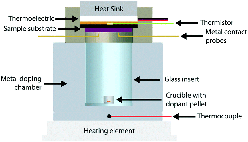 | ||
| Fig. 1 Cross section of apparatus for vapor doping experiments. Metal doping chamber houses glass insert with alumina crucible and F4TCNQ pellet within. F4TCNQ pellet is vaporized by heating the metal doping chamber to a desired temperature on a hot plate, whose temperature in monitored by a thermocouple in the base. The sample is simultaneously measured and held stable by the metal contact probes, and a thermoelectric holds the temperature of the sample to a set constant from 0 °C to 70 °C. All vapor doping experiments were performed in an argon glovebox. | ||
The sample holder has a thermoelectric module (Peltier) for active temperature control of the thin film sample (Tfilm). The thermoelectric module, coupled with a water-cooling heat sink, permitted a stable operational range from 0 °C to 70 °C. This temperature was measured using a thermistor that was thermally connected to the sample substrate, and thus ensured stable temperature measurement and control of the sample directly. Two stainless-steel probes allowed for electrical contact with the sample during vapor doping.
The doping chamber was designed for controlled sublimation of dopant by heating at the ambient pressure of the glovebox. The chamber housing is made of stainless-steel metal, which is in constant thermal contact with the heating source (ceramic hotplate). A cylindrical glass insert is placed in the center of the doping chamber to house the dopant source, which is placed on the bottom as a pellet in an alumina crucible. A thermocouple is placed near the dopant source at the base of the metal chamber to monitor the dopant sublimation temperature (Tdopant), which was fixed to 200 °C in this study unless otherwise stated.
P3HT–F4TCNQ in situ conductivity
To study vapor doping conductivity in situ, thin film P3HT was doped with F4TCNQ with Tfilm = 0, 30, and 70 °C. This range of temperatures is significant for probing the vapor doping process of P3HT above and below the Tg of the polymer backbone, which is known to be around 20 °C (dependent on the molecular weight and regioregularity).35 Another potential effect would rely on how quickly the diffusion into the polymer would occur; one hypothesis is that at higher Tfilm, the diffusion would occur more quickly and would accelerate the rise of σ.Using an interdigitated electrode device, the σ of the thin film can be tracked from its beginning to its end over six orders of magnitude. σ of P3HT was measured while doping with F4TCNQ up until 20 min, at which point all curves had established an equilibrium σ.
Representative curves at these three different Tfilm can be seen in Fig. 2. A common pattern appears for all three temperatures, which looks similar to the standard relation between σ and dopant concentration published many times prior.3,30,36 The σ profile shows a significant rise upon the film's first introduction to dopant, exponentially climbing around five orders of magnitude in around a minute, then slows to climbs linearly, and finally reaches a maximum electronic conductivity (σmax) within four minutes. Past this point, the magnitude of the σ drops, which previously has been attributed to the oversaturation of the dopant degrading the order of the polymer, which in turn reduces the mobility of the charge carriers in the material.27
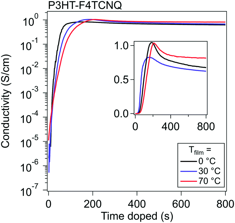 | ||
| Fig. 2 In situ conductivity curves of F4TCNQ-doped P3HT. The σ for P3HT over the course of doping with F4TCNQ is shown for three different Tfilm. The semilog plot shows that σ rises five orders of magnitude in around two minutes, and the linear inset details the form of the drop in σ past σmax. | ||
A few comparisons stand out between the three Tfilm. The σmax and general trends are almost identical between runs at the different Tfilm. Tfilm = 0 °C reached a σmax about a minute faster than the films at Tfilm = 30 °C and Tfilm = 70 °C. We hypothesize that the difference in the timing of σmax (tmax) is attributed to the adsorption of vaporized dopant occurring more quickly due to the larger temperature gradient between dopant and film. Across five runs, σmax,0°C = 2.9 ± 0.29 S cm−1, σmax,30°C = 2.38 ± 0.26 S cm−1, and σmax,70°C = 1.34 ± 0.04 S cm−1; this shows a trend of σ rising highest when Tfilm is the lowest, but in general σmax does not vary much from Tfilm to Tfilm. The lack of strong temperature dependence on the conductivity curve indicates that the dopant diffusion does not depend on the backbone Tg for fast diffusion, likely passing through the space provided by the low Tg alkyl sidechains. Post σmax, the films retain over 70% of their σmax once they stabilize out, which, in these experiments, did not differ consistently with Tfilm.
In order to probe the universality of the σ profile, a few further in situ conductivity experiments were conducted using the P3HT–F4TCNQ system. In the first experiment, we reduced the sublimation temperature of the dopant (Tdopant) from 200 °C to 160 °C. We did this to test if a slower sublimation rate would change the trends of the in situ σ curve. These doping curves at Tdopant = 160 °C showed a similar σmax to curves with Tdopant = 200 °C. When the doping curve for Tdopant = 160 °C was scaled by sublimation rate, its shape closely matched curves with the standard Tdopant = 200 °C, as seen in Fig. S4B.†
The melt-crystallized film showed a slightly higher and more stable σmax and slower tmax compared to the “soft” annealed films. We hypothesize that the higher and more stable σ is due to the melt-crystallized P3HT having a higher fraction of crystalline domains. The overlap of the highest occupied molecular orbital (HOMO) of the aggregate-P3HT with the lowest unoccupied molecular orbital (LUMO) of the F4TCNQ is stronger than that of the amorphous-P3HT HOMO with the F4TCNQ LUMO and should result in a higher number of charge carriers generated overall with better stability of the reaction between the dopant and polymer.37
Stabilization of conductivity at specific doping times.
We conducted in situ conductivity experiments where the sample was doped to specific doping times. These curves were shown in Fig. 3 at the same three Tfilm as the in situ conductivity experiments. This figure was constructed as such: the solid black curve is the in situ conductivity profile as shown in Fig. 2, and the dotted, colored curves represent samples doped to the doping times at 50 s intervals (e.g. red is doped to 50 s, orange to 100 s), and show the stabilization of the σ after the sample was taken off the dopant.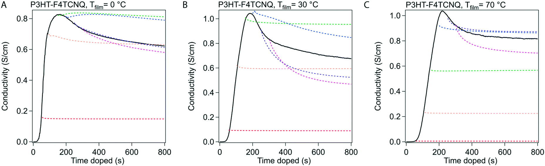 | ||
| Fig. 3 Stabilization of σ at 50 s intervals. Samples of P3HT were doped with F4TCNQ at 50 s intervals as to replicate the conditions of samples that were taken off at that time for other experiments, such as UV-vis, Raman spectroscopy, and grazing incidence wide angle X-ray scattering. The dotted line indicates the shape of the σ curve when the sample is taken off at the beginning of the dotted line (i.e. the red dotted line was curtailed at 50 s). The solid line indicates the in situ curve of σ. | ||
In Fig. 3, the samples stabilized before and after tmax show different behavior in σ. For samples doped to a time before tmax (e.g. 50 s, 100 s), the drop in σ resolves quickly and retains most of the σ during stabilization. For samples doped to a time closer to, and especially after tmax, relatively large reductions occur in σ (∼80 to 90% of the initial σ at that specific doping time) that take minutes to stabilize. We hypothesize from this transition that tmax represents a tipping point towards a small decrease in σ, whether through a reduction in charge carriers or the mobility of those charge carriers.
Absorption measurements of P3HT–F4TCNQ track fraction of doped sites to in situ σ curve
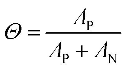
To gain further insight into the nature of the shape of the in situ doping curve, we used UV-vis-NIR spectra to determine a relative measure of doping level.Fig. 4A shows the UV-vis-NIR absorption for a P3HT film doped in 50 s intervals, from neat to 300 s for Tfilm = 0 °C (Fig. S5† shows the spectra for Tfilm = 30, 70 °C). The black curve, for the neat polymer, shows a peak at 2.3 eV that corresponds to the primary absorption peak for neutral P3HT. Upon doping, peaks at 0.5 and 1.5 eV appear, which correspond to allowed sub-gap transition bands in positive polarons, as well as peaks at 1.4 and 1.6 eV, which come from the F4TCNQ radical anion and is indicative of an integer charge transfer doping mechanism.30,38 Murrey et al. use a parameter Θ, which they define as the fraction of doped P3HT sites over the total available P3HT sites. They linearly approximate this from the absorption using the equation
 | (1) |
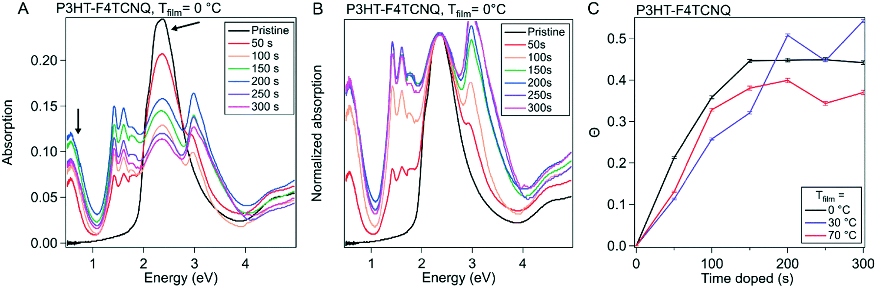 | ||
| Fig. 4 UV-vis-NIR absorption of P3HT and P3HT–F4TCNQ samples. (A) Representative absorption spectra of P3HT–F4TCNQ films doped to the levels shown in Fig. 3 (0 s to 300 s at 50 s intervals), with sample temperature 0 °C, shown normalized to the neutral P3HT peak at 2.3 eV in (B). The peak at 0.5 eV is attributed to the polaron and the peak at 2.3 eV is attributed to the neutral P3HT. (C) Plotting the fraction of doped P3HT sites (Θ) versus the doping time. The value of Θ is correlated to charge carrier concentration. | ||
As the amount of time doped increases, the neutral P3HT peak at 2.3 eV is bleached while the peaks attributed to the doped material increases.40 It appears that the rise in Θ slows, then hits a maximum at the tmax in its corresponding in situ conductivity experiment (150 s or 200 s doped). After this maximum, Θ equilibrates or reduces slightly. All three Tfilm show similar values for Θ as well as the overall trend, which corresponds to their similarity for the in situ conductivity experiments.
Local molecular ordering of polymer closely correlates to σ
To provide more context to how the dopant situates and interacts with the ordered domains of the polymer film, we used grazing incidence wide angle X-ray scattering (GIWAXS). The molecular packing structure of P3HT is well documented, as well as its reaction to the infiltration of molecular dopant in both solution sequential and vapor sequential doping methods.27,30,40 Qualities such as long-range ordering and the π–π stacking spacing are determinants on how efficiently charges can be conducted via inter- and intra-chain mechanisms; F4TCNQ has been shown to intercalate into the alkyl-stacking of the polymer during vapor doping, as well as reduce the π–π stacking spacing, increasing π–π orbital overlap and leading to better interchain conduction.412D GIWAXS scattering images from these experiments can be seen in Fig. S7–S9† for Tfilm = 0, 30 and 70 °C respectively. 1D scattering profiles were obtained via radial integration of the 2D scattering images, which are displayed in Fig. 5A–C. The strong features primarily seen in the qz direction that are equally spaced out correspond to the lamella-stacked side chains (h00). The broad ring that stretches both in and out of the plane of scattering is the (020) peak, which is associated with the π–π stacking direction. In our analysis, resolving the individual peaks further out in reciprocal-space is difficult, so the maximum scattering spacing was used as an estimate of the average spacing distance. The alkyl sidechain stacking distance and the π–π stacking distance are plotted versus doping time in Fig. 5D and E, respectively.
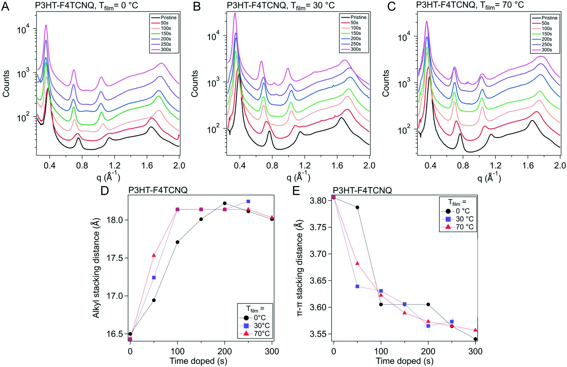 | ||
| Fig. 5 Evolution of ordered structures over the course of doping. Grazing incidence wide angle X-ray scattering (GIWAXS) was conducted on P3HT vapor doped with F4TCNQ at 50 s intervals from 0 s to 300 s for all three sample temperatures. (A)–(C) show the azimuthal linecuts of the scattering images, such as the ones seen in Fig. S10.† (D) Shows the evolution of the alkyl-stacking spacing, which are represented in the linecuts as the first three, equal spaced out peaks. (E) Shows the π–π stacking, which is represented by the broad peak originating around 1.6 Å−1 in the neat film. | ||
Qualitatively, the scattering trends seen here are consistent to the reported results in literature. Upon doping, the sidechain/alkyl stacking and the π–π stacking distances do not drastically change; the (h00) peaks' position decreases in reciprocal space, corresponding to a larger spacing between the sidechains. This increase in the alkyl stacking distance increases at a higher rate from the onset of doping to 150 s, dependent on Tfilm, which corresponds to tmax in our in situ experiments. Quantitatively, for the P3HT–F4TCNQ with Tfilm = 0 °C, the alkyl stacking spacing (d100) changes from 1.64 nm to 1.80 nm. Concurrently, the π–π stacking peak position increases in reciprocal space, indicating a decrease in packing spacing in the π–π direction. Although the spacing dropped quickly in the first 100 s of doping, the change in spacing slows down as the doping reaches σmax as seen in the in situ conductivity experiment. For the P3HT–F4TCNQ at Tfilm = 0 °C, the π–π stacking spacing reduced from d020 = 0.381 nm to 0.355 nm over the course of 300 s vapor doping.
Resonance Raman spectroscopy of P3HT–F4TCNQ show evolution of doping in ordered and amorphous domains
Raman spectra are very sensitive to π-electrons due to their polarizability under photoexcitation.42,43 We use this phenomenon along with resonance Raman techniques to capture the evolution of various fractions of the polymer film. By using an excitation laser that matches the energy of the polaronic (charged) polymer, we can preferentially probe structural changes arising from these features.44 This can be executed using a 785 nm laser (1.58 eV) that lines up with the second polaronic absorption and dopant anion peaks (see Fig. S6†).The Raman spectra from the 785 nm excitation laser can be seen in Fig. 6A and S10.† These spectra were obtained on P3HT–F4TCNQ films vapor doped in 50 s intervals, from neat to 300 s, at the three Tfilm as the in situ conductivity experiments. The spectra in these figures are focused on the 1300 to 1600 cm−1 range, which features peaks that correspond to the C![[double bond, length as m-dash]](https://www.rsc.org/images/entities/char_e001.gif) C intraring vibration modes which are sensitive to the charging of the conjugated thiophene backbone.
C intraring vibration modes which are sensitive to the charging of the conjugated thiophene backbone.
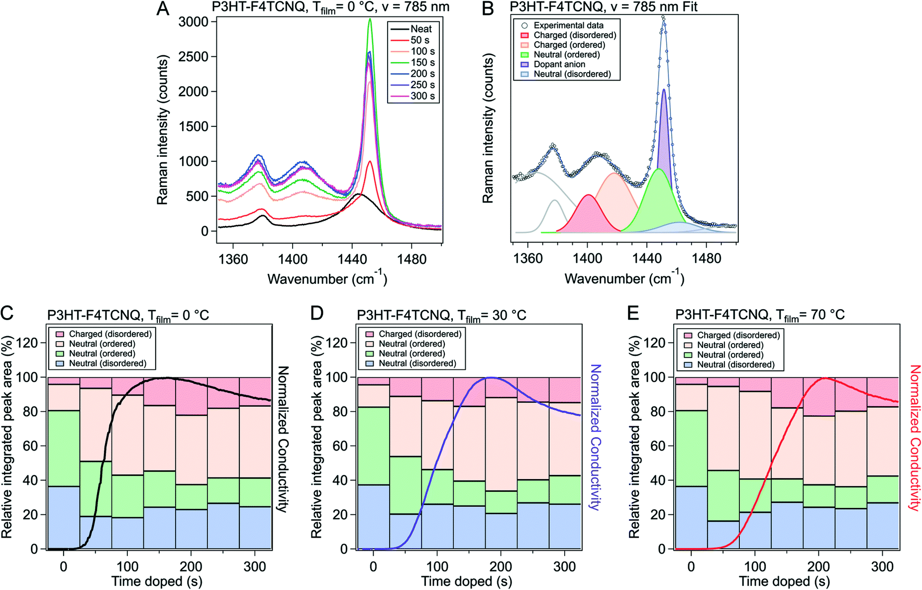 | ||
| Fig. 6 Raman spectra and peak fitting for P3HT–F4TCNQ samples doped to different levels. (A) Raman measurements were conducted on P3HT–F4TCNQ films doped to the levels shown in Fig. 3 (0 s to 300 s at 50 s intervals), using an excitation wavelength of 785 nm. (B) Peak fittings were made according to the methodology introduced in ref. 42. (C–E) The peak areas from the fittings were taken, and ratios of integrated peak area fitted were calculated, for Tfilm = 0, 30, & 70 °C respectively. The in situ σ curves for the respective Tfilm is overlayed for easier comparison. More detailed descriptions of the fitting methods are described in Fig. S11 and Tables S1 through S4.† | ||
To accurately track the relative concentration of certain fractions over the course of doping, the spectra were fit to peaks that were described by Nightingale et al. Peaks corresponding to the CC intraring vibration of the neutral fractions were centered around 1455 cm−1, with a peak from the neutral, ordered domains around 1447 cm−1 and a peak from the neutral, disordered domains around 1462 cm−1 (Fig. 6B and S9†). Changes in peak position and shape were attributed to changes in conjugation length (i.e., conformational order), with lower wavenumbers corresponding to longer conjugation length (hence why the disordered polymer peak sits at a higher wavenumber than the ordered).42 The peak widths and peak locations were given bounds to account for changes in the mean and distribution in conjugation lengths; these bounds were sourced from Nightingale et al.42 Due to the resonance of the charged domains of the film, we can also resolve the charged ordered and charged disordered domains of the films, whose peaks sit at roughly 1417 cm−1 and 1401 cm−1, respectively. These peaks were allowed to change in both peak width and position more widely, due to expected changes in the mean and standard deviation of conjugation lengths in the charged polymer as dopant infiltrated and interacted with the polymer film. A more detailed discussion of the fitting methodology, parameters, and data can be found alongside Fig. S11 and Tables S1–S3 in the ESI.†
The relative integrated peak area from the fits of the 785 nm excited Raman for Tfilm = 0, 30, and 70 °C is plotted in Fig. 6C–E respectively. The relative integrated peak area was obtained by dividing the integrated area of the peak in question by all the peaks attributed to the polymer in its spectrum's fit; this was done in order to track the relative changes of each peak over the course of doping, dividing out the increase of the total absorption due to resonance with the polymeric polaron.
Due to the presence of the dopant anion peak (1451 cm−1) over the neutral, ordered, and neutral, disordered peaks, we chose to focus our analysis primarily on the evolution of the charged, ordered and charged, disordered peaks. Comparing the ratio of charged peaks to neutral peaks (roughly correspondent to Θ in our UV-vis-NIR analysis), the ratio is highest at tmax (∼200 s) and decreases slightly from that maximum at higher doping times. However, the greatest increase in charged, ordered peak area comes from the step from the neat film to the 50 s doped film, whereas charged, disordered appears to increase steadily with time, with its maximum corresponding to tmax and the highest ratio of charged to neutral peak area. The decrease in the ratio also appears to be primarily due to a loss in peak area for the charged, disordered peak, whereas the charged, ordered relative peak area stays relatively constant.
To recontextualize, these results indicate that the dopant first preferentially infiltrates and reacts with the ordered domains, which are energetically more favorable to interact with than the disordered domains. This rapid reaction with the ordered domain also corresponds with the exponential rise in conductivity, over five orders of magnitude, for the first 50 s. The slower, linear rise of conductivity can be attributed to the increase in charge carrier concentration in the disordered domains, and the final stabilization to a lower σ also can be attributed to a loss of charge carrier concentration in the disordered domains.
These results build upon what has been with previously shown in P3HT Raman literature. In a blend P3HT/PCBM film, Gao et al. show via 473 nm resonance Raman a broadening of the “aggregate P3HT” peak around 1450 cm−1 as F4TCNQ loading increases, which we would attribute to an increase in the charged ordered peak.18 Chew et al. corroborate this finding using a 532 nm excitation focusing on the neutral aggregates, claiming an increase in conjugation length of the neutral aggregates with the presence of F4TCNQ dopant.45 Lim et al. use an off-resonance laser wavelength of 633 nm that averages over the entire film, and show that both RR and RRa P3HT have a stiffening of the backbone with the presence of F4TCNQ.27 This phenomenon was shown to also exist in polythiophenes with polar sidechains by Ma et al., where P3MEET shows a lower conjugation length than P3HT, but similarly stiffens in the presence of dopant.46
Conclusions
This study investigated vapor doping of P3HT with F4TCNQ in order to understand the evolution of conductivity in situ and the corresponding structural changes at the molecular level. The temporal profile of σ first exhibited a rapid exponential increase, followed by a short linear increase until reaching a σmax, and finally followed by a slow decay in σ. While the profile and range of σ are comparable for each Tfilm (0, 30, 70 °C) investigated, tmax was achieved the fastest at Tfilm = 0 °C where the temperature difference between the Tdopant and Tfilm was the largest. For in situ conductivity experiments where the sample was doped to a specific time, the decay and stabilization of σ was dependent on the proximity to tmax. Specifically, samples doped close to and after tmax demonstrated the largest decay in σ.The characterization of the vapor doped P3HT thin films through UV-vis-NIR spectroscopy, and GIWAXS provided complementary insight on the extent of doping. Analysis of the UV-vis-NIR spectra reveal the doping level (based on the fraction of doped sites, Θ), increases linearly until hitting a maximum near tmax in its corresponding in situ σ curve after which the doping level stabilized. By monitoring d100 and d020 from the GIWAXS results showed the changes to these characteristic spacings from the infiltration of dopant anion in crystalline domains stabilizes near tmax of the in situ doping curve – consistent with the UV-vis-NIR data.
Resonant Raman spectroscopy experiments provided deeper insights on the relative extent of doping within the crystalline (ordered) and amorphous (disordered) domains and their connection to the in situ conductivity profile. Specifically, at 785 nm, the spectra revealed relative fraction of neutral ordered, charged ordered, neutral disordered, charged disordered components in the thin films. At 50 s, doping preferentially occurred in the ordered domains leading to a larger relative charged ordered fraction while only a small fraction of charge is formed in the amorphous domains. As the doping time was increased, the propensity of doping was still in the ordered domains and accounts for the rapid rise in σ until approaching tmax. In the context of the in situ conductivity profile, this corresponded to the transition point where the conductivity changes linearly and reaches σmax. In this transition regime, the crystalline domains reached their saturated doping (charged) level and subsequent doping only occurred at sites in the disordered domains.
This method of comparing these characterization techniques to the in situ/ex situ σ curves has been fruitful in providing more granular insight into the processes of vapor molecular doping. Going forward, this platform is readily available for use for more novel polymer-dopant combinations. Further insight into how different sidechains or functional groups on the backbone effects the in situ σ, and how this is reflected in further characterization, will help to realize materials with better stability and higher σ with better understanding on how the polymer chemistry and structure affect the molecular doping process.
Methods
Materials and sample preparation
All substrates used for grazing incidence wide angle X-ray scattering (GIWAXS), Raman spectroscopy, atomic force microscopy (AFM) and UV-vis-NIR absorption spectroscopy in this study were cleaned by ultrasonication in acetone and 2-propanol for 15 minutes each. GIWAXS measurements were performed on films deposited on Si substrates with 1.5 nm of native SiO2. UV-vis absorption, Raman measurements, and AFM were performed on films deposited on top of quartz substrates. Conductivity measurements were performed on films deposited on custom-fabricated interdigitated gold electrodes (IDEs), which in turn is on Si substrates with 1000 nm of thermally-grown SiO2. Solutions of 91% to 94% regioregular poly(3-hexylthiophene-2,5-diyl) (RR-P3HT) (Rieke Metals) were prepared by dissolving P3HT in anhydrous chlorobenzene at 10 mg mL−1. The mixed solutions were shaken overnight before being spun onto the prepared substrates. The substrates were spin coated with solution at 2000 rpm at 45 seconds, then at 3000 rpm for 25 seconds. IDEs were cleaned of excess polymer with cotton swabs to reduce leakage current.In situ conductivity setup
For the in situ conductivity measurements, a specialized setup was fabricated for control and precision of measurement. A steady-state temperature is achieved using a thermoelectric module. The sample is held in place by two electrode probes, which allows for electrical contact with the sample during vapor doping. See Fig. 1 for a cross section of the setup, and Fig. S3† for a more detailed 3D rendering.Vapor doping process
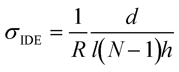
Vapor doping of F4TCNQ was performed in an argon-filled glovebox. Approximately 5 mg of dopant was pressed into a pellet and placed in an aluminum oxide crucible (OD 6.8 mm × H 4 mm from Government Scientific Source Inc.), which was in turn placed in a glass insert (diameter ∼5 cm, height ∼4.5 cm). A stainless-steel container is then preheated to allow the chamber to reach the desired temperature, which is monitored by thermocouple, and the glass insert is placed inside the container, at which point the setup is allowed to stabilize in temperature. A Teflon cap is placed upon the opening of the glass insert to block dopant from polluting the glovebox.All samples used for doping were placed within the sample holder. Electrical contact was made to the sample through the sample holder, which was then routed via cables through the back of the glovebox to a BioLogic SP-200 Potentiostat. A voltage of 100 mV is applied to the sample, and the current through the sample is measured by the potentiostat every second. These data are converted from current to resistance and then conductivity through the equation:
Conflicts of interest
There are no conflicts to declare.Acknowledgements
M. F. D. acknowledges support from the National Science Foundation (NSF) Graduate Research Fellowship under Grant No. DGE-1746045. This work made use of the shared facilities at the University of Chicago Materials Research Science and Engineering Center, supported by the National Science Foundation under award number DMR-2011854. Parts of this work were carried out at the Soft Matter Characterization Facility of the University of Chicago. This research used resources of the Advanced Photon Source, an Office of Science User Facility operated for the U.S. Department of Energy (DOE) by Argonne National Laboratory under Contract No. DE-AC02-06CH11357. The authors thank Ban Xuan Dong for providing the IDEs used in this study.References
- I. E. Jacobs, E. W. Aasen, J. L. Oliveira, T. N. Fonseca, J. D. Roehling, J. Li, G. Zhang, M. P. Augustine, M. Mascal and A. J. Moulé, J. Mater. Chem. C, 2016, 4, 3454–3466 RSC.
- D. T. Scholes, S. A. Hawks, P. Y. Yee, H. Wu, J. R. Lindemuth, S. H. Tolbert and B. J. Schwartz, J. Phys. Chem. Lett., 2015, 6, 4786–4793 CrossRef CAS PubMed.
- S. N. Patel, A. M. Glaudell, K. A. Peterson, E. M. Thomas, K. A. O'Hara, E. Lim and M. L. Chabinyc, Sci. Adv., 2017, 3, e1700434 CrossRef PubMed.
- I. E. Jacobs and A. J. Moulé, Adv. Mater., 2017, 29, 1703063 CrossRef PubMed.
- P. Y. Yee, D. T. Scholes, B. J. Schwartz and S. H. Tolbert, J. Phys. Chem. Lett., 2019, 10, 4929–4934 CrossRef CAS PubMed.
- D. T. Scholes, P. Y. Yee, J. R. Lindemuth, H. Kang, J. Onorato, R. Ghosh, C. K. Luscombe, F. C. Spano, S. H. Tolbert and B. J. Schwartz, Adv. Funct. Mater., 2017, 27, 1702654 CrossRef.
- S. N. Patel, A. M. Glaudell, D. Kiefer and M. L. Chabinyc, ACS Macro Lett., 2016, 5, 268–272 CrossRef CAS.
- M. S. AlSalhi, J. Alam, L. A. Dass and M. Raja, Int. J. Mol. Sci., 2011, 12, 2036–2054 CrossRef CAS PubMed.
- J.-H. Bahk, H. Fang, K. Yazawa and A. Shakouri, J. Mater. Chem. C, 2015, 3, 10362–10374 RSC.
- L. Huang, Z. Hu, J. Xu, K. Zhang, J. Zhang, J. Zhang and Y. Zhu, Electrochim. Acta, 2016, 196, 328–336 CrossRef CAS.
- R. Meerheim, C. Körner and K. Leo, Appl. Phys. Lett., 2014, 105, 063306 CrossRef.
- T. Ma, B. X. Dong, G. L. Grocke, J. Strzalka and S. N. Patel, Macromolecules, 2020, 53, 2882–2892 CrossRef CAS.
- S. D. Kang and G. J. Snyder, Nat. Mater., 2017, 16, 252–257 CrossRef PubMed.
- D. Venkateshvaran, M. Nikolka, A. Sadhanala, V. Lemaur, M. Zelazny, M. Kepa, M. Hurhangee, A. J. Kronemeijer, V. Pecunia, I. Nasrallah, I. Romanov, K. Broch, I. McCulloch, D. Emin, Y. Olivier, J. Cornil, D. Beljonne and H. Sirringhaus, Nature, 2014, 515, 384–388 CrossRef CAS PubMed.
- P. Pingel and D. Neher, Phys. Rev. B: Condens. Matter Mater. Phys., 2013, 87, 115209 CrossRef.
- K. E. Watts, B. Neelamraju, E. L. Ratcliff and J. E. Pemberton, Chem. Mater., 2019, 31, 6986–6994 CrossRef CAS.
- B. Neelamraju, K. E. Watts, J. E. Pemberton and E. L. Ratcliff, J. Phys. Chem. Lett., 2018, 9, 6871–6877 CrossRef CAS PubMed.
- J. Gao, J. D. Roehling, Y. Li, H. Guo, A. J. Moulé and J. K. Grey, J. Mater. Chem. C, 2013, 1, 5638 RSC.
- S. Olthof, W. Tress, R. Meerheim, B. Lüssem and K. Leo, J. Appl. Phys., 2009, 106, 103711 CrossRef.
- I. Salzmann, G. Heimel, M. Oehzelt, S. Winkler and N. Koch, Acc. Chem. Res., 2016, 49, 370–378 CrossRef CAS PubMed.
- D. Kiefer, R. Kroon, A. I. Hofmann, H. Sun, X. Liu, A. Giovannitti, D. Stegerer, A. Cano, J. Hynynen, L. Yu, Y. Zhang, D. Nai, T. F. Harrelson, M. Sommer, A. J. Moulé, M. Kemerink, S. R. Marder, I. McCulloch, M. Fahlman, S. Fabiano and C. Müller, Nat. Mater., 2019, 18, 149–155 CrossRef CAS PubMed.
- O. Zapata-Arteaga, B. Dörling, A. Perevedentsev, J. Martín, J. S. Reparaz and M. Campoy-Quiles, Macromolecules, 2020, 53, 609–620 CrossRef CAS PubMed.
- T. J. Aubry, K. J. Winchell, C. Z. Salamat, V. M. Basile, J. R. Lindemuth, J. M. Stauber, J. C. Axtell, R. M. Kubena, M. D. Phan, M. J. Bird, A. M. Spokoyny, S. H. Tolbert and B. J. Schwartz, Adv. Funct. Mater., 2020, 30, 2001800 CrossRef CAS PubMed.
- R. Noriega, J. Rivnay, K. Vandewal, F. P. V. Koch, N. Stingelin, P. Smith, M. F. Toney and A. Salleo, Nat. Mater., 2013, 12, 1038–1044 CrossRef CAS PubMed.
- C. Wang, D. T. Duong, K. Vandewal, J. Rivnay and A. Salleo, Phys. Rev. B: Condens. Matter Mater. Phys., 2015, 91, 085205 CrossRef.
- J. Hynynen, D. Kiefer, L. Yu, R. Kroon, R. Munir, A. Amassian, M. Kemerink and C. Müller, Macromolecules, 2017, 50, 8140–8148 CrossRef CAS PubMed.
- E. Lim, A. M. Glaudell, R. Miller and M. L. Chabinyc, Adv. Electron. Mater., 2019, 5, 1800915 CrossRef.
- P. Carbone and A. Troisi, J. Phys. Chem. Lett., 2014, 5, 2637–2641 CrossRef CAS PubMed.
- M. T. Fontana, D. A. Stanfield, D. T. Scholes, K. J. Winchell, S. H. Tolbert and B. J. Schwartz, J. Phys. Chem. C, 2019, 123, 22711–22724 CrossRef CAS.
- E. Lim, K. A. Peterson, G. M. Su and M. L. Chabinyc, Chem. Mater., 2018, 30, 998–1010 CrossRef CAS.
- K. Kang, S. Watanabe, K. Broch, A. Sepe, A. Brown, I. Nasrallah, M. Nikolka, Z. Fei, M. Heeney, D. Matsumoto, K. Marumoto, H. Tanaka, S. Kuroda and H. Sirringhaus, Nat. Mater., 2016, 15, 896–902 CrossRef CAS PubMed.
- C. Poelking and D. Andrienko, Macromolecules, 2013, 46, 8941–8956 CrossRef CAS.
- C. Scharsich, R. H. Lohwasser, M. Sommer, U. Asawapirom, U. Scherf, M. Thelakkat, D. Neher and A. Köhler, J. Polym. Sci., Part B: Polym. Phys., 2012, 50, 442–453 CrossRef CAS.
- J. Gierschner, Y.-S. Huang, B. Van Averbeke, J. Cornil, R. H. Friend and D. Beljonne, J. Chem. Phys., 2009, 130, 044105 CrossRef PubMed.
- R. Xie, Y. Lee, M. P. Aplan, N. J. Caggiano, C. Müller, R. H. Colby and E. D. Gomez, Macromolecules, 2017, 50, 5146–5154 CrossRef CAS.
- H. Shirakawa, E. J. Louis, A. G. MacDiarmid, C. K. Chiang and A. J. Heeger, J. Chem. Soc., Chem. Commun., 1977, 578 RSC.
- S. Sweetnam, K. R. Graham, G. O. Ngongang Ndjawa, T. Heumüller, J. A. Bartelt, T. M. Burke, W. Li, W. You, A. Amassian and M. D. McGehee, J. Am. Chem. Soc., 2014, 136, 14078–14088 CrossRef CAS PubMed.
- K.-H. Yim, G. L. Whiting, C. E. Murphy, J. J. M. Halls, J. H. Burroughes, R. H. Friend and J.-S. Kim, Adv. Mater., 2008, 20, 3319–3324 CrossRef CAS.
- T. L. Murrey, M. A. Riley, G. Gonel, D. D. Antonio, L. Filardi, N. Shevchenko, M. Mascal and A. J. Moulé, J. Phys. Chem. Lett., 2021, 12, 1284–1289 CrossRef CAS PubMed.
- H. Méndez, G. Heimel, S. Winkler, J. Frisch, A. Opitz, K. Sauer, B. Wegner, M. Oehzelt, C. Röthel, S. Duhm, D. Többens, N. Koch and I. Salzmann, Nat. Commun., 2015, 6, 8560 CrossRef PubMed.
- X. Shen, V. V. Duzhko and T. P. Russell, Adv. Energy Mater., 2013, 3, 263–270 CrossRef CAS.
- J. Nightingale, J. Wade, D. Moia, J. Nelson and J.-S. Kim, J. Phys. Chem. C, 2018, 122, 29129–29140 CrossRef CAS.
- T. Degousée, V. Untilova, V. Vijayakumar, X. Xu, Y. Sun, M. Palma, M. Brinkmann, L. Biniek and O. Fenwick, J. Mater. Chem. A, 2021, 9, 16065–16075 RSC.
- J. Wade, S. Wood, D. Beatrup, M. Hurhangee, H. Bronstein, I. McCulloch, J. R. Durrant and J. Kim, J. Chem. Phys., 2015, 142, 244904 CrossRef PubMed.
- A. R. Chew, R. Ghosh, Z. Shang, F. C. Spano and A. Salleo, J. Phys. Chem. Lett., 2017, 8, 4974–4980 CrossRef CAS PubMed.
- T. Ma, B. X. Dong, J. W. Onorato, J. Niklas, O. Poluektov, C. K. Luscombe and S. N. Patel, J. Polym. Sci, 2021, 59, 2797–2808 CrossRef CAS.
- D. Sharon, P. Bennington, C. Liu, Y. Kambe, B. X. Dong, V. F. Burnett, M. Dolejsi, G. Grocke, S. N. Patel and P. F. Nealey, J. Electrochem. Soc., 2018, 165, H1028–H1039 CrossRef CAS.
- Z. Jiang, X. Li, J. Strzalka, M. Sprung, T. Sun, A. R. Sandy, S. Narayanan, D. R. Lee and J. Wang, J. Synchrotron Radiat., 2012, 19, 627–636 CrossRef CAS PubMed.
- P. Hu, K. Du, F. Wei, H. Jiang and C. Kloc, Cryst. Growth Des., 2016, 16(5), 3019–3027 CrossRef CAS.
Footnote |
| † Electronic supplementary information (ESI) available. See DOI: https://doi.org/10.1039/d1me00192b |
| This journal is © The Royal Society of Chemistry 2022 |