
Thermal behavior and polymorphism of 2,9-didecyldinaphtho[2,3-b:2′,3′-f]thieno[3,2-b]thiophene thin films†
Felix
Talnack
 ab,
Sebastian
Hutsch
bc,
Michael
Bretschneider
d,
Yulia
Krupskaya
d,
Bernd
Büchner
d,
Marc
Malfois
e,
Mike
Hambsch
ab,
Frank
Ortmann
bc and
Stefan C. B.
Mannsfeld
*ab
ab,
Sebastian
Hutsch
bc,
Michael
Bretschneider
d,
Yulia
Krupskaya
d,
Bernd
Büchner
d,
Marc
Malfois
e,
Mike
Hambsch
ab,
Frank
Ortmann
bc and
Stefan C. B.
Mannsfeld
*ab
aFaculty of Electrical and Computer Engineering, Technische Universität Dresden, 01062 Dresden, Germany. E-mail: Stefan.mannsfeld@tu-dresden.de
bCenter for Advancing Electronics Dresden (cfaed), Technische Universität Dresden, 01062 Dresden, Germany
cDepartment of Chemistry, Technische Universität München, 85748 Garching b. München, Germany
dLeibniz Institute for Solid State and Materials Research Dresden, IFW, Helmholtzstraße 20, 01069, Dresden, Germany
eALBA Synchrotron, Carrer de la Llum 2-26, 08290 Cerdanyola del Vallès, Barcelona, Spain
First published on 31st January 2022
Abstract
The ability of numerous organic molecules to adopt different crystal structures without changing their chemical structure is called polymorphism which has gained interest in recent years due to the influence it has on the solid-state properties of organic materials, e.g. charge transport in organic semiconductors. Here we present a new polymorphic crystal structure of the p-type small molecule semiconductor 2,9-didecyldinaphtho[2,3-b:2′,3′-f]thieno[3,2-b]thiophene (C10-DNTT). The polymorphic transition is observed during heating the films over 400 K and investigated by in situ cross-polarized optical microscopy (CPOM) and in situ grazing-incidence wide-angle X-ray scattering (GIWAXS) measurements. From these measurements, we refine the thin-film crystal structure of both the low temperature and high temperature polymorphs. We further analyze the thermal expansion of both polymorphs and perform density-functional theory (DFT) calculations to trace back the anisotropic thermal expansion to anisotropic molecular interactions.
Design, System, ApplicationPolymorphic phase transitions in small molecule organic semiconductors have been extensively studied in recent years. This is due to the potential of increasing the device performance significantly if a beneficial crystal structure of a material can be identified and be produced or stabilized in the active device thin film. On the other hand, phase transitions of materials are often accompanied by strong changes in the morphology, i.e. cracking due to thermal stress and dewetting. If these effects happen in an already fabricated electrical device, the performance is severely diminished and special measures should be taken in order to avoid them. Here we investigate the small molecule 2,9-didecyldinaphtho[2,3-b:2′,3′-f]thieno[3,2-b]thiophene (C10-DNTT), which due to its low solubility has to be processed around temperatures close to a newly found polymorphic phase transition, which is described here for the first time. This in-depth analysis of the transition and the thermal expansion behavior of C10-DNTT can be used as the foundation for the development of design strategies to either promote or hinder polymorphic phase transition in DNTT or similar rod-like small molecules with solubilizing side-chains. This will lead to better performance and stability in devices comprising organic semiconductors. |
Introduction
Together with benzothieno[3,2-b][1]benzothiophene (BTBT) derivatives, naphtho[2,3-b]naphtho[2′,3′:4,5]thieno[2,3-d]thiophene (DNTT) derivatives have been in the center of research as active materials in high performance organic thin film transistors.1–6 Especially with the solution-processable derivatives of DNTT and BTBT, very good performances have been achieved.7,8Notably, for the small molecule 2,9-didecyldinaphtho[2,3-b:2′,3′-f]thieno[3,2-b]thiophene (C10-DNTT), mobilities higher than 10 cm2 V−1 s−1 were achieved in thin film transistors. Combined with the low contact resistance, this makes C10-DNTT a promising candidate for high frequency applications, e.g. for wireless communication.9 The cores of these molecules facilitate a high overlap of the π–π orbitals and therefore a high charge carrier mobility perpendicular to the molecular planes.8 This results in strong van der Waals forces between the molecules, which in turn leads to low solubility in organic solvents. The introduction of alkyl chains in the case of 2,7-dioctyl[1]benzothieno[3,2-b][1]benzothiophen (C8-BTBT) increases the solubility enough to process it from solution at high concentrations in a variety of commonly used solvents. On the other hand, for DNTT derivatives with the introduction of even longer alkyl chains to the core, the solubility at room temperature in commonly used solvents, e.g. toluene or chloroform, is too small for an efficient and simple fabrication of thin films.10 In order to overcome this challenge, special measures have to be taken. An increase of solubility can be achieved by heating the solution. In the case of C10-DNTT in toluene, the saturation concentration is below 0.9 mg ml−1 at 373 K.11 Because the solubility drops significantly at lower temperatures, the solution processing step has to be performed at temperatures around 373 K and higher, as well.8,12 Other recent approaches to fabricate C10-DNTT thin films from solution include processing at very slow coating speeds below 10 μm s−1,13 several coating steps,14 modifying the coating setup e.g. heating the blade as well as the substrate in blade coating,14 or using edge casting techniques with slow processing speeds.15,16 More drastic approaches include modifying the structure of the side chains or the core shape.1,2,17 Additionally, post-deposition thermal annealing of the films is a standard practice in order to improve the ideality of the devices by improving the interfaces between the semiconductor, contacts and dielectric, respectively.14,16,18 Even for thermal deposition under high-vacuum, the optimal substrate temperature for C10-DNTT is reported to be 353 K, after which the charge carrier mobility in the films drops significantly.12 The wide range of temperatures and processing parameters used in fabrication have a drastic effect on the device performance. Together with the many reports in the literature about polymorphism in similar rod-like molecules,4,19–21 this makes it desirable to investigate the morphology and crystal structure of C10-DNTT thin films at those temperatures which are routinely used during and after solution processing.
In this paper, we employ grazing-incidence wide-angle X-ray scattering (GIWAXS), cross-polarized optical microscopy (CPOM), and atomic force microscopy (AFM) to investigate thermally induced changes in the structure of C10-DNTT thin films. From the obtained GIWAXS data, we refined two different crystal structures at two different temperatures. Refinement at room temperature resulted in a phase similar to the one reported by Nakayama et al. from bulk crystals.16 At elevated temperatures, a different diffraction pattern appeared that led to a significantly changed crystal structure. Furthermore, we observed a strong anisotropy in the thermal expansion of the two in-plane unit cell axes a and b, for both polymorphs. In order to understand this anisotropy, we performed density-functional theory (DFT)-based simulations. The simulations show that this is caused by different molecular interactions in these directions. Additionally, we were able to show that the two polymorphs show different vibrational mode patterns, which might cause the different thermal expansion behavior of the two polymorphs.
Cross-polarized optical microscopy
In order to obtain information about any macroscopic changes in the morphology or crystallinity of C10-DNTT thin films during heating and cooling, we took cross-polarized optical microscopy images at different temperatures. For this, we used the solution processed thin films with large ribbon-like crystallites that cover the entire substrate. These ribbons are several hundred micrometers wide and therefore easily observable at low magnification levels.The thin films were heated stepwise from room temperature up to 465 K and images were taken at fixed intervals. The heating rate was 2 K min−1 and the dwell time at each temperature was approximately 300 seconds. The images obtained during the heating and subsequent cooling procedure are shown in Fig. 1. At room temperature, large crystallites with the distinct ribbon-like morphology can be observed which are typical for meniscus-guided coated films with a coating speed in the evaporative regime. On top of these ribbons, smaller crystallites form, which are typical for solution-processed C10-DNTT films.12,13,22 The ribbons show two distinct colors at room temperature, a greenish yellow and a bright orange, which indicates that for the two ribbons the fast-growing and slow-growing crystal axes are orientated differently with respect to the polarization of the incoming light. Up to a temperature of 375 K, no significant change regarding color or intensity in the microscopy images can be observed and the amount of cracks visible in the films stays constant. However, for temperatures higher than 375 K the color of the orange ribbons turns into dark purple, whereas the green crystallites do not show a significant color change. We attribute this change of color in the orange/purple ribbon to a change in the birefringence of the crystals, which is caused by a reorientation of the molecules inside the thin film. The green ribbons do not undergo a color change to the same extent as the orange/purple ribbon, because the crystals are orientated in such a way towards the polarizer, that a reorientation of the molecules will not alter the birefringence significantly. This is supported by the cross-polarized images taken from the same area, but with the substrate rotated by 45°, as shown in Fig. S1.† Upon rotation, the orange ribbons change their color to green and no significant change in color is visible upon heating the samples. This observation also rules out the possibility that the color change was due to thin film interference effects in conjunction with thickness changes upon heating, since then the color change would be observable for the samples rotated by 45° as well. We assert that this reorientation is due to a polymorphic transition of C10-DNTT to a new polymorph, which we will call high temperature (HT) polymorph II in the following. In addition to the change in color, extensive cracking in the film can be observed when the films are heated above this transition temperature. During the subsequent cooling, a transition back to the original colors occurs, again at around 375 K.
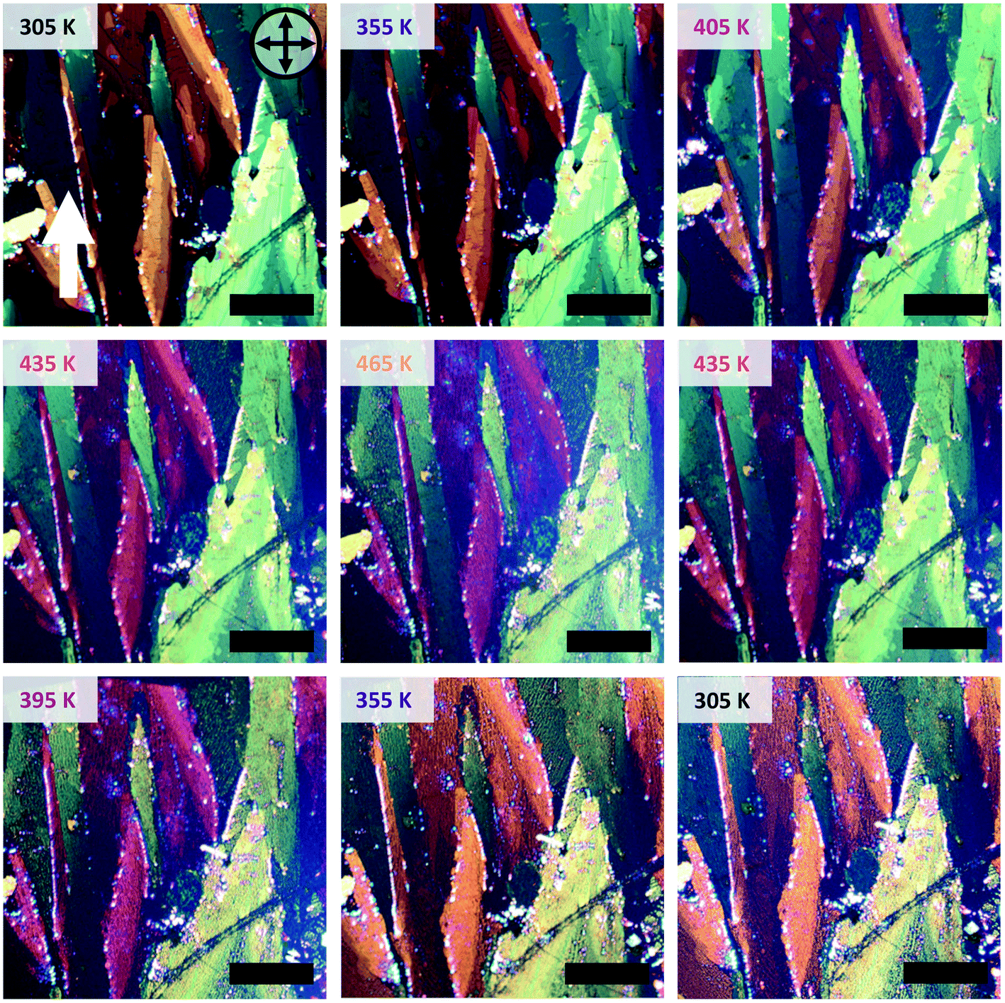 | ||
| Fig. 1 Cross-polarized optical microscopy images of shear-coated C10-DNTT thin films during heating and cooling. The color change of the ribbon from orange to purple and back from 405 K and 395 K during heating and cooling, respectively, indicates a change in crystal structure. The shear-coating direction is indicated by the white arrow. The scale bar corresponds to 400 μm. | ||
Grazing-incidence wide-angle X-ray scattering with in situ heating
In order to gain insights into the corresponding temperature dependence of the molecular-level packing in the solution processed and evaporated thin films, we performed grazing-incidence wide-angle X-ray scattering (GIWAXS) experiments with in situ heating. For the main part of this investigation, we used vacuum-deposited 25 nm thick C10-DNTT thin films on silicon wafers. This fabrication technique leads to many small crystallites with no preferred in-plane orientation. This is usually referred to as a 2D-powder, for which we assume that the crystallites are so small that all orientations are equally probed during exposure of the samples to X-rays in a grazing-incidence configuration. This allows us to analyze the peak intensities of the obtained scattering images without the need to rotate the sample simultaneously. Solution processed samples were also investigated, but the large area and the high degree of in-plane texture of the large crystallites, while beneficial for the cross-polarized optical microscopy images, render these samples anisotropic in regard to rotation around the substrate normal. This effect can be accounted for by rotating the sample 360° during illumination, but this was not possible with the available heating setups.In Fig. 2, the 2D-detecor GIWAXS images that were obtained during heating and cooling are shown. The peak indexing and extraction of the unit cell parameters was performed by a least-squares-error optimization procedure with the convention that the a and b axes are parallel to the substrate plane. The indexed 2D image of a room temperature measurement is shown in Fig. S2† and the calculated unit cell parameters are shown in Table 1. In order to compare our results for thin films to the results obtained by Nakayama et al. for bulk crystals, we calculated the theoretically expected 2D scattering image of the reported crystal structure.16 A comparison between the calculated 2D image and an image of a C10-DNTT film measured at room temperate is shown in Fig. S3.† The diffraction patterns in the images are quite similar which leads us to the conclusion that the thin film phase and the single crystal phase of C10-DNTT are almost identical. We attribute the minor changes between the literature bulk crystal structure and our thin film structure to thermal expansion and substrate induced effects.23 Because of these small differences and considering the overall similarity, we decided to call the crystal structure that was indexed and refined in this work at low temperatures as polymorph Ib and the literature bulk phase as Ia.
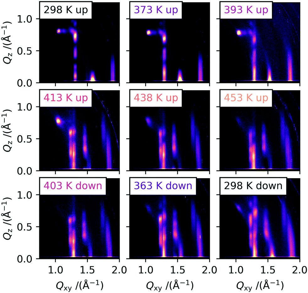 | ||
| Fig. 2 2D scattering images obtained by GIWAXS measurements at different temperatures of evaporated C10-DNTT thin films. A clear change in the diffraction pattern can be observed above 400 K, which persists to over 453 K and during cooling down to room temperature. | ||
| Literature16,a | Polymorph Ibb | Polymorph IIc | |
|---|---|---|---|
| a Literature unit cell parameters indexed from a bulk crystal measurement obtained at 200 K. b Unit cell parameters of low temperature polymorph Ib indexed from room temperature GIWAXS data. The difference between the low temperature unit cell parameters obtained from the literature and our experiments is attributed to thermal expansion and substrate induced effects. c Unit cell parameters of the high temperature polymorph II obtained from GIWAXS measurements at 443 K. The indexed GIWAXS images of polymorph Ib and II are shown in Fig. S2.† | |||
| a/(Å) | 5.99 | 6.09 ± 0.02 | 6.28 ± 0.07 |
| b/(Å) | 7.62 | 8.03 ± 0.07 | 8.95 ± 0.06 |
| c/(Å) | 38.04 | 37.93 ± 0.10 | 37.43 ± 0.38 |
| α/(°) | 90.00 | 90.9 ± 0.3 | 90.3 ± 0.3 |
| β/(°) | 94.5 (85.5) | 86.3 ± 0.2 | 86.8 ± 0.4 |
| γ/(°) | 90.0 | 90.1 ± 0.5 | 92.8 ± 0.5 |
| In-plane area/(Å2) | 45.7 | 48.9 ± 0.5 | 56 ± 2 |
| Volume/(Å3) | 1731.8 | 1850.0 ± 18 | 2096 ± 35 |
The GIWAXS measurements recorded at higher temperatures are shown in the following images of Fig. 2. The samples were heated on a heating stage with a rate of 5 K min−1 and a dwell time of 60 s before each measurement, and then exposed for 30 s. During the heating procedure, a shift of the peaks towards smaller Q-values can be observed, especially for the Bragg rods at Qxy = 1.3 Å−1, 1.6 Å−1 and 1.9 Å−1, stemming from the thermal expansion of the unit cell. However, around 400 K the obtained scattering images start to change drastically. The single Bragg rod at Qxy = 1.3 Å−1 for the 11l and 1−1l reflections starts to split into two Bragg rods with Qxy values of 1.23 Å−1 and 1.28 Å−1. This indicates a change of the in-plane γ angle. Additional peaks start to appear on the 02l rod (Qxy = 1.46 Å−1) at higher Qz values, which showed only a single peak at low temperatures close to the “horizon” (Qz ≈ 0.0 Å−1). This rod does not split into two rods as it has only a contribution from the b-axis and is therefore unaffected by a change in γ. For the 21l Bragg rod around 1.9 Å−1 again the splitting into two Bragg rods can be observed at higher temperatures.
At all temperatures during heating, low intensity peaks at the original positions for the low temperature (LT) polymorph Ib can be observed, indicating the presence of still unconverted crystallites of the original polymorph. We suggest that the unconverted crystallites are located as the first monolayer (ML) on the substrate, as they would not produce higher order reflections and have a streak-like appearance located close to the “horizon”. The first ML of many organic semiconductors is more strongly bound due to interactions with the substrate in comparison to the following multilayers, which is shown by a drastic increase in desorption temperature.24,25 The increase in binding energy will also have a significant effect on the transition temperature. Additionally, in a measurement with the temperature above the transition point of 375 K with extensive beam damage, only ML-typical streaks at the Bragg rod positions of polymorph Ib were observed. The corresponding images are shown in Fig. S4.† We hypothesize that this is due to the destruction of the molecular layers by the beam propagating from the top downwards. For areas without extensive beam damage, the diffraction pattern of the HT polymorph II is still clearly visible at 473 K, showing the high temperature stability of the material itself.26
During the cooling shown in Fig. 2, the reflections from the HT polymorph are clearly visible at all temperatures down to room temperature. The peaks shift back to larger Q-values, because of the shrinking of the unit cell with the decrease in temperature. Based on the CPOM results shown earlier, one might expect a transition back to the original LT polymorph Ib to be visible also in the GIWAXS data after cooling past the transition temperature measured before. However, this was not observed, but around 373 K, the peaks attributed to polymorph Ib start to gain in intensity but do not become stronger than the peaks originating from polymorph II until cooling below room temperature. The reason for this very likely lies in the difference in film thickness between the thick films used for the CPOM investigation and the much thinner films used for the GIWAXS study. Diao et al. have shown that the hysteresis of the temperature cycle can be increased by reducing the film thickness.27 The proposed nanoconfinement effectively reduces and constrains certain molecular degrees of freedom and in doing so hinders the transition to an energetically more favorable crystal structure, stabilizing a meta-stable polymorph. In their study, the hysteresis of a TIPS-pentacene phase transition between polymorph I and IIb can be reduced from 26 K for 300 nm thick films to over 80 K for 30 nm thick films.
The unit cell parameters were extracted from the scattering images at room temperature for polymorph Ib and at 443 K for polymorph II, respectively. The 2D images from which the peak positions were extracted with the indexed reflections are shown in Fig. S2.† In Table 1 the values of both unit cells are listed, together with the unit cell parameters reported in the literature.16 As expected the values for the a and b axes change towards larger values due to the thermal expansion of the unit cell. The difference between the in-plane unit cell axes a and b between polymorph Ib and II is minor compared to the significant change in the γ angle between them. The long c-axis does not significantly differ between polymorph Ib and II.
We performed in- and out-of-plane cuts through the data in order to analyze in more detail the change in peak position during the heating/cooling cycle. The results are shown in Fig. 3. Discussing the in-plane peak positions first, the peak splitting for the peaks at Qxy = 1.3 Å−1 and 1.9 Å−1 can be clearly seen from 423 K onwards. Additionally, the shift to smaller Q-values with increasing temperature as caused by thermal expansion can be seen. The splitting of the two Bragg rods stays visible even when the samples are completely cooled down to room temperature again. For the 02l Bragg-rod at roughly Qxy = 1.5 Å−1, a second peak appears which we attribute to polymorph Ib crystallites which converted back during cool down or were not converted during the heating.
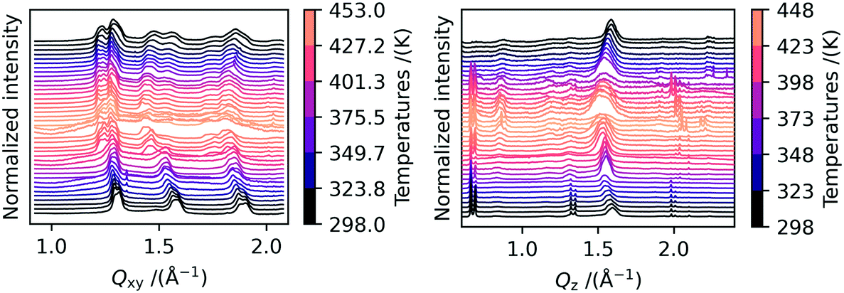 | ||
| Fig. 3 On the left, in-plane cuts of the 2D scattering images obtained during in situ heating GIWAXS measurements are shown. A clear splitting of the peak at 1.2 Å−1 can be observed at elevated temperatures. The shift of the peaks during heating and subsequent cooling is due to thermal expansion and contraction. On the right, out-of-plane cuts at different temperatures are shown. No shift in the position of the 00l peaks is visible, which indicates that the inter-distance stacking does not change with temperature. | ||
In Fig. 3, the out-of-plane peak positions of the 00l Bragg rod at different temperatures are shown on the right side. We observe that some peaks change their position upon heating. The peaks located at Qz = at 0.7 Å−1, 0.8 Å−1 and 1.1 Å−1 do not change position with increasing temperature, whereas the high intensity peaks at Qz = 1.3 Å−1 and 1.5 Å−1 move towards smaller Q-values during heating and to larger Q-values during cooling. This leads us to conclude that these peaks originate from crystals with different structures or orientations. The two peaks at Qz = 1.3 Å−1 and 1.5 Å−1 are very intense and vanish first upon heating. In the AFM images shown in Fig. S5b),† nanostructures can be seen which also disappear upon heating to high temperatures, and we therefore attribute these peaks to these nanostructures. Interestingly, the two out-of-plane peaks at Qz = 1.3 Å−1 and 1.5 Å−1 show the same dependence of intensity on temperature as the two in-plane peaks at Qxy = 1.3 Å−1 and 1.5 Å−1. The good agreement in peak position in combination with the identical thermal behavior strongly suggests that the nanostructures are polymorph Ib crystallites that grow vertically on top of the film. In these crystallites, the molecules are aligned such that they adopt a lying-down geometry relative to the substrate plane. The out-of-plane peaks at Qz = 1.3 Å−1 and 1.5 Å−1 can thus be identified as the 110 and 020 reflections from these crystallites. In Fig. S5,† we included a sketch of the film composition in combination with a scattering image, in which the peak origins are highlighted. Finding such rotated crystallites is in agreement with recent reports from Peng et al.22 We can therefore assume that only the non-shifting peaks at Qz = at 0.7 Å−1, 0.8 Å−1 and 1.1 Å−1 belong to the 00l Bragg rod. Since these do not change their peak positions during heating or cooling, we conclude that the interlayer distance of the C10-DNTT films stays constant during heating or cooling. In Table 1, it can be seen that neither the length of the c-axis nor the α and β angles are significantly different when comparing the two polymorphs and the literature phase. Here it should be noted that due to the large length of the c-axis and the low number of peaks visible in the diffraction images, the α and β angles are difficult to extract with high precision from the 2D images.
In order to test how a capping layer on top of C10-DNTT might affect the polymorphic transition and whether or not it can protect the film from beam damage and potential loss of material due to unwanted sublimation, a protective polystyrene (PS) capping layer was also tried on otherwise identical samples. The corresponding GIWAXS images are shown in Fig. S6.† The films undergo the same phase transition as the films without a capping layer at around 403 K and also exhibit a large hysteresis, as the diffraction pattern of polymorph II is still visible after cooling the films down to room temperature. In Fig. S7,† further cooling to 278 K and a time series of images taken at a 30 min interval at room temperature is shown. The HT polymorph II still persisted down to 278 K and it was only after letting the films rise to room temperature again that the diffraction pattern of polymorph Ib started to dominate again. After 30 min, almost no contributions of polymorph II can be seen in the diffraction patterns. The conversion from the high temperature polymorph back to the low temperature polymorph upon cooling shows that the polymorphs are enantiotropically linked. This can also be seen in the DSC trace reported by Kang et al.28
Thin film structure refinement
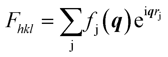
In order to obtain the full crystal structures of polymorph Ib and II including the molecular packing, we refined the structures from the obtained diffraction patters. For the LT polymorph Ib we used the data measured at room temperature and for the HT polymorph II we used the data collected at 443 K. The used images are shown in Fig. S2.† For the refinement procedure, we extracted the intensity for each peak from the corrected and background subtracted diffraction image. From the intensities of the peaks, we can gain information of the molecular orientation inside the unit cell since within the kinematic approximation, the maximum intensity of a diffraction peak can be calculated from the structure factors Fhkl using eqn (1): | (1) |
 describes the scattering of the molecule by summing up the individual contributions of the single atoms j at their respective positions rj. The first part fj describes the atomic scattering factors.
The crystal structures were determined by calculating the crystallographic residual  . The observed structure factor Fobs is calculated from the observed intensity as explained previously and compared to the structure factor Fcalc, which is calculated from the refined structure. With the help of Wq an individual weight to every peak intensity can be applied and the scale factor k is described by
  .31 A detailed description of the refinement procedure on the example of TIPS-pentacene and TIPS-thiotetracene is given by Mannsfeld et al.32
When crystal structures are refined from single crystals or powders, the number of measurable or absent reflections is often high enough to fit the data well despite the high number of degrees of freedom during the fit. In order to get reasonable results with the limited amount of peaks we observe, a couple of assumptions need to be made. We assume that there are two molecules in each unit cell, which is reasonable regarding the unit cell volume of 1850 Å3 at room temperature and 2100 Å3 at 443 K, which are listed in Table 1, and the volume of a single molecule of 865 Å3 and considering thermal expansion. The volume of a single molecule was estimated from the electron density with Gaussian 16.33 Secondly, we keep the position of the center of mass of these two molecules fixed in the unit cell at high symmetry positions, assuming that they both rest in the a–b-plane forming densely packed a–b sheets. Thus, for the calculations one molecule is positioned at 0/a, 0/b and 0/c and the second molecule is positioned at the relative unit cell coordinates 0.5/a, 0.5/b and 0/c. The shape of the molecules is obtained from bulk crystal data.16 If we were to keep the molecular geometry rigid, the six Euler angles of the two molecules would thus be the only fitted parameters. However, if the entire molecular geometry is kept rigid, most importantly the connection between the core and the alkyl chain, only specific orientations of the molecules would be possible in which both the core and the alkyl chains of both molecules are parallel. In order to lift this artificial restriction and the emulate the conformational flexibility often found in alkyl chains, we treat the first carbon atom of the alkyl chain like a “ball joint” within which the rest of the chain can be freely rotated. A sketch of the molecules in the unit cell with the introduced “ball joints” is shown in Fig. S8b).† This allows for a free rotation of the alkyl chain around three axes and therefore new orientations of the cores with parallel side chains are possible, leading to a total of 12 fitted parameters. To illustrate the benefit of introducing this additional degree of freedom per alky chain, the refined structures for polymorph Ib and II with stiff side chains are shown in Fig. S9† for comparison.
The refined structure of polymorph Ib is shown in Fig. 4a). It can be seen that the molecules are orientated in a herringbone packing motif, which was already expected by the missing 01 L and 10 L Bragg rods in the scattering images. Additionally, the long axis of the molecules is orientated in the same direction as the long c-axis of the unit cell, which was also expected due to their similarity in length. The alkyl chains are pointing away from the rest of the core. The agreement between the obtained crystal structure and the one described in the literature is good, showing that the crystal structure in thin films at room temperature and bulk crystals are similar. Fig. 4a) also shows the observed intensities and the calculated intensities obtained from the refined structures.
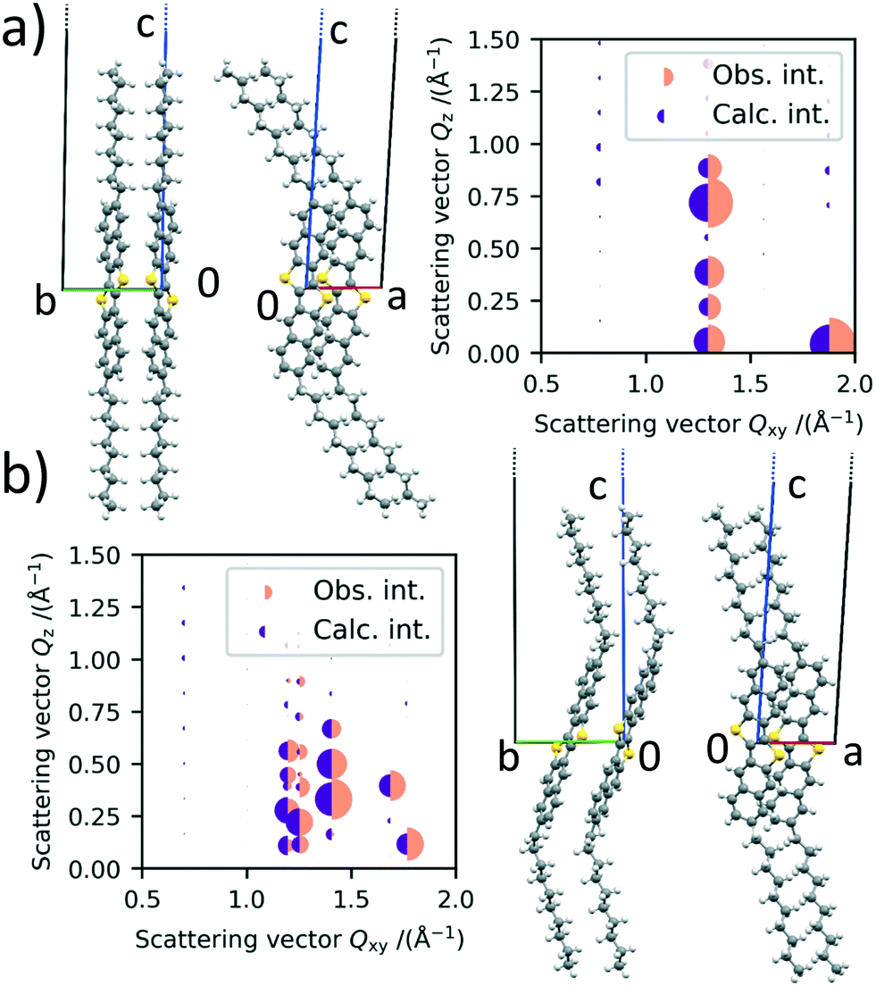 | ||
| Fig. 4 a) Refined crystal structure for the low temperature polymorph Ib and the corresponding intensity profiles. b) Refined crystal structure for the high temperature polymorph II and the corresponding intensity profiles. The observed and calculated intensities are represented by the radii of the orange and purple half circles, respectively. The green b-axis and the red a-axis are located in the substrate plane. | ||
According to Purdum et al., the absence of short interlayer contacts indicates that the crystal structure is meta stable and therefore might change upon a post-deposition treatment e.g., thermal or solvent-vapor annealing.34 In the case of the low temperature phase, there are no short C–H contacts between two molecule layers, neither in the crystal structure reported in the literature nor in our refined structure. This is in agreement with our observation that the low temperature phase undergoes a phase transition upon heating and is therefore metastable.
For the HT polymorph II, the same refinement is performed and the molecular packing is shown in Fig. 4b). Due to the change in γ and the following splitting of the Bragg rods, we were able to extract the intensity of more peaks from the scattering image, leading to a statistically even more dependable refinement process. The molecules are still packed in a herringbone fashion towards each other and the angle between them does not change significantly. The cores of the molecules however are tilted significantly towards the b axis in the HT crystal structure. The tilt of the cores towards the a unit cell axis does not change. The inter-layer distance does not change between polymorph Ib and II, as a rotation of the alkyl chains cancels the rotation of the core towards the b axis.
Thermal expansion and simulation
On the basis of the large number of data obtained during the heating cycles, we can also analyze the thermal expansion characteristics of polymorph Ib before the phase transition and the thermal contraction characteristics of polymorph II before its transition back to polymorph Ib during cooling.In Fig. 5a) the thermal expansion of the in-plane unit cell parameters is plotted. It can be seen that for the LT polymorph the a-axis expands by 0.0008 ± 0.0002 Å K−1 and the b-axis by roughly three times more namely 0.0024 ± 0.0003 Å K−1 in the investigated temperature range during heating. In the following we want to investigate this anisotropy of the thermal expansion for the a and b axes of the unit cell. For HT PII we investigated the contraction of the unit cell during cooling, as we have more data points in this direction at our disposal. The anisotropy is even stronger than for polymorph Ib, with the a-axis almost staying constant and even slightly increasing during cooling with an expansion coefficient of −0.0002 ± 0.0001 Å K−1. For the b axis we found a decrease in length during cooling with an expansion coefficient of 0.0013 ± 0.0002 Å K−1. In Fig. 5b) the in-plane areas of the respective polymorphs at different temperatures are shown. It can be seen that the area thermal expansion coefficient of the high temperature polymorph II is smaller than the expansion of the first polymorph. The larger fluctuations in the measurements are caused by the realignment of the sample stage during the GIWAXS measurements, which is necessitated by the thermal expansion of the measurement setup.
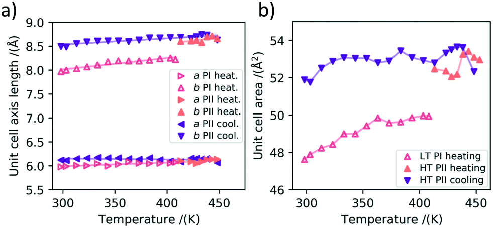 | ||
| Fig. 5 a) Lattice constants a and b during heating (▷, △) and cooling (◁, ▽). The filled triangles denote the high temperature polymorph II. It can be seen that the change in length is stronger for the b-axis in both polymorphs upon heating and cooling. b) The in-plane unit cell areas of both polymorphs plotted against the temperature. The filled in triangles denote polymorph II. | ||
To understand the experimentally observed anisotropy in the thermal expansion we also performed simulations based on density-functional theory (DFT). To this end, we checked the simulated anisotropy in the expansion of the unit cell and relate it to the anisotropy in the molecular vibrations.
In the first step, we analyzed the anisotropic expansion of the unit cell as the anisotropic response of the system to an artificial increase of the unit cell volume. The principle of the simulation is sketched in Fig. 6a. The simulations start with the experimentally resolved unit cells (lattice + atomic positions) of the respective phase, henceforth defined by the unit cell volume V0 and lattice vectors a and b. In the first step, the unit cell volume is artificially increased by a factor xi (e.g. xi = 1.05 for an increase of the volume by 5%), which is evenly distributed over a and b. Next, a constant volume relaxation of both the lattice and atomic positions is performed with DFT as implemented in VASP.35 That is, the volume of the unit cell is kept constant during the relaxation, but the shape and therefore lattice vectors may change. As a consequence, the artificial increase of the unit cell volume will distribute anisotropically over the lattice vectors due to the anisotropic molecular interactions. The resulting expansion in a and b directions with respect to the volume increase is presented in Fig. 6 for the LT phase (b) and HT phase (c). A clear anisotropy between a and b directions is observable for both phases similar to the experiment. For the LT phase, the anisotropy can be quantified by calculating the linear change of the lattice vectors with respect to the volume increase. These coefficients compute to  and
and  , being 4 times larger in the b direction than in the a direction, in decent agreement to the experimentally observed anisotropy of αIb/αIa ≈ 3. A similar calculation can be performed for the HT phase (see values in c), however since the initial volume V0 of the thermally expanded HT phase is far from the DFT equilibrium, the results are more qualitative than quantitative in nature. Interestingly, the calculations, which used the refined crystal structure of polymorph II, reproduce the negative expansion coefficient of the a-axis, which we observed experimentally as an expansion of the unit cell in this direction during cooling. Capturing this effect confirms that the crystal structure refinement procedure extracted HT polymorph II reasonably well. Please note that the inclusion of a temperature-dependency to the expansion, e.g. by calculating the free energy for every volume Vi using the quasi-harmonic approximation,36 is prohibitive due to the large amount of atoms in the unit cell and the flexible C10 side-groups, which lead to significant numerical uncertainties in the required free energy. A further study of anharmonic vibrational effects causing the thermal expansion is prohibitive for similar reasons.
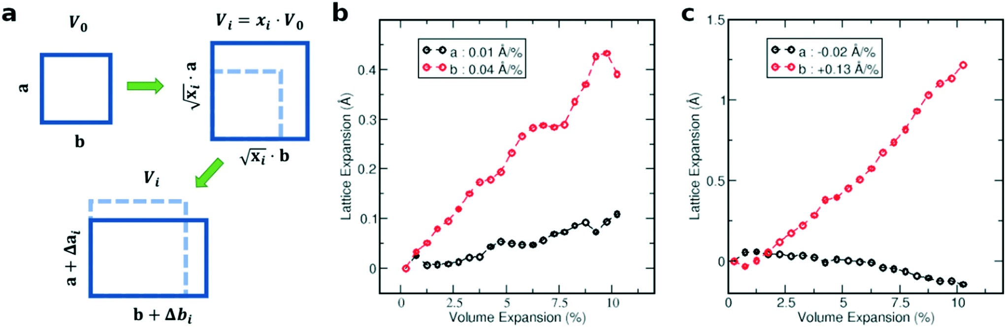 | ||
| Fig. 6 Simulation of the anisotropic lattice expansion. a) Scheme of the simulation procedure for an exemplary 2D unit cell. As a first step, the volume is expanded and in a second step, the anisotropy of the expansion of the a and b unit cell axis is calculated. b and c) Simulated lattice expansion in a and b directions with respect to the volume expansion for the LT phase (b) and HT phase (c), showing the anisotropic expansion of the a- and b-axes. The values for the linear change of the axis length are shown in the inset. | ||
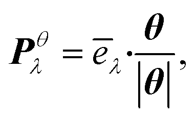
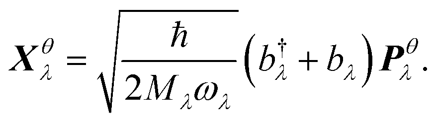
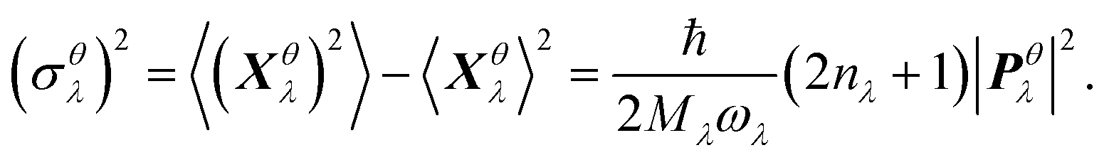
We thus study the anisotropy of the molecular vibrations within the harmonic approximation, which is computationally feasible. To this end, we treat the molecular vibrations as quantum-harmonic oscillators and analyze the anisotropic fluctuations 〈(Xθλ)2〉 − 〈Xθλ〉2 in the displacement Xθλ of these oscillators in θ = a and θ = b directions. The necessary crystal mode patterns for both the LT and HT phases were obtained via a normal mode analysis with periodic density-functional tight binding theory37 (DFTB) using DFTB+.38 To ensure that the unit cell consists of one neighboring molecule in both a and b directions, the experimental unit cell was doubled in the a direction. The normal mode analysis yields a set of crystal modes λ at the Γ point defined by their vibration frequencies ωλ and normalized polarization vectors ēλ (which is represented as a matrix containing the displacement of every atom in the three cartesian directions). To analyze the anisotropy between a and b, we computed the projection of ēλ onto the normalized lattice vectors θ = a, b:
 | (2) |
 | (3) |
 | (4) |
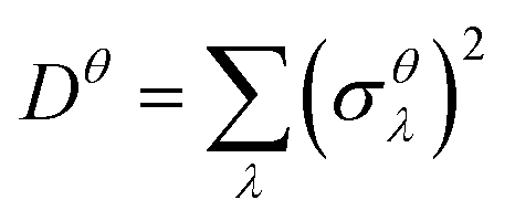 as a sum of all normal modes for both the LT and HT phases in a and b directions. For the LT phase we obtain DaLT = 32 Å2 and DbLT = 36 Å2, while for the HT phase we obtain DaHT = 23 Å2 and DbHT = 33 Å2. That is, for both phases anisotropy is observable, whereby the fluctuation of the displacement is stronger in the b direction than in the a direction. This affirms that the molecules are more weakly bound in the b direction than in the a direction, enabling the more pronounced thermal expansion in the b direction observed in the experiment and simulation above.
We finally show in Fig. 7 the mode patterns of the vibrations that contribute most to the displacement fluctuations in the b direction for the LT phase (a) and HT phase (b). The arrows represent the direction of movement of each atom and the length represents the relative weight of the atom in the polarization vector ēλ. We find that for the LT phase the dominating vibration is an intramolecular butterfly mode showing an anti-parallel vibration of the DNTT core and the C10 side-chains. In contrast, for the HT phase, the dominating mode is intermolecular and the cores are vibrating in an anti-parallel fashion in the direction of the long molecule axis in a slipping motion. As a consequence, we find that the phase transition from the LT to HT phase, despite retaining the herringbone packing motif, significantly changes the intermolecular vibrations. The reason therefore is probably the changes in the side-chain orientations, which alter the intermolecular interactions and structural constraints in the molecular motion. It is thus not surprising to observe significantly different thermal expansion behaviors for both polymorphs in both the experiment and simulation.
 | ||
| Fig. 7 Visualization of the polarization vectors that contribute most to the deflection in the b-direction (arrow in the center) for the LT phase in (a) and HT phase in (b). The mode patterns of the vibration change from an intramolecular anti-parallel motion between the cores and the alkyl chains in (a) to an intermolecular shear vibration between the molecules in (b). | ||
Summary and conclusion
In summary, we presented an unreported polymorph of the small molecule semiconductor C10-DNTT and investigated the new polymorph in detail with different methods including in situ heating grazing-incidence wide-angle X-ray scattering and density-functional theory based simulations. From the X-ray data, the crystal structure of both the known low temperature phase and the high temperature polymorph was refined in its thin film form. Additionally, the thermal expansion of the unit cell of C10-DNTT is investigated. Experimentally, we found a strong anisotropy in the thermal expansion of the in-plane unit cell axes and can explain it, based on our simulations, with the strong difference in molecular interactions in these directions. We were also able to predict qualitatively the expansion of the a- and b-axes by using our refined crystal structures, which are in agreement with our experimental findings.The discovery of a polymorph of C10-DNTT poses an important step towards fully understanding film formation, degradation and the resulting performance fluctuations of devices employing this and materials with similar structures. Due to its easily accessible high temperature polymorph, C10-DNTT is a good candidate for further investigations regarding polymorphic transitions in its material class. The detailed analysis of the thermal behavior of the thin films will help to improve the thermal stability of devices in order to make organic devices even more stable and reliable in the future.
Experimental section
Materials
The self-assembled monolayer materials (SAM) phenyltrichlorosilane (PTCS) and octadecyltrimethoxysilane (ODMTS) were purchased from Sigma-Aldrich. 2,9-Didecyldinaphtho[2,3-b:2′,3′-f]thieno[3,2-b]thiophene (C10-DNTT) was purchased from Lumtec and used without further purification.Film fabrication
We investigated thin films that were fabricated by both thermal vacuum deposition and solution processing. For the thermally evaporated films, first an octadecyltrimethoxysilane (ODTMS; Sigma Aldrich) self-assembled monolayer (SAM) was deposited on silicon wafers with a native oxide as described in the literature.39 After that, a layer of C10-DNTT (Lumtec) with a nominal thickness of 25 nm was deposited on the substrate under high vacuum at a rate of 0.25 Å s−1. For the solution processed thin films, we employed solution shearing in which a thin film is deposited on a substrate by moving a solution reservoir across the sample with a blade angled at 8° and at a defined gap of 100 μm to the substrate. This results in a meniscus in front of the blade at whose tail end molecules start to aggregate and finally crystallize into a solid film. Before the solution shearing procedure, the substrate was prepared by depositing a self-assembled monolayer of trichlorophenylsilane (PTCS; Sigma Aldrich). The advantage of the solution shearing method is the possibility to obtain millimeter-sized, single crystalline domains, which are observable with light microscopy at low magnifications. A detailed description of the shear coating setup, procedure, and the accompanying surface modifications can be found in the literature.40GIWAXS measurements
Preliminary in situ heating GIWAXS experiments were performed at the Sirius beamline at the SOLEIL synchrotron in Paris, France. The main part of the in situ heating GIWAXS investigations was performed at the NCD-SWEET beamline of the ALBA synchrotron. An area detector (LX255-HS, Rayonix) was placed approximately 14–20 cm (depending on the desired q-range) behind the sample, which was mounted on top of a Linkam heating stage. In order to minimize any oxidative beam damage from the prolonged exposure to X-rays in combination with increased temperatures, nitrogen was blown onto the samples and the sample position was changed periodically to a fresh area. The beam size was 80 μm horizontally and 30 μm vertically and the beam energy was 12.4 keV. The incidence angle was 0.12°; the collected images were calibrated using a chromium oxide calibration standard and background-subtracted using background images from a silicon wafer samples treated with ODTMS. A scaling factor for the background subtraction was obtained by measuring the integrated background intensities in an area without diffraction peaks for both images. Due to the data being recorded in grazing-incidence geometry with a flat 2D area detector, the raw data has to be corrected.32 To facilitate direct measurements of scattering vectors, the raw images are converted to Q-space with orthogonal in-plane (Qxy) and out-of-plane (Qz) components. The conversion and correction procedure was described by Mannsfeld et al.41 The GIWAXS data was corrected and analyzed with WxDiff.47Simulations
The constant-volume relaxation of the unit cell to study the anisotropic expansion for different initial volumes is performed with periodic density functional theory (DFT) and the VASP program package.35 The calculations were performed based on the PBE42 functional and the inclusion of Grimme's DFT-D3 dispersion correction43 to account for van der Waals interactions.Due to the elevated system size of C10-DNTT with 4 molecules per unit cell (384 atoms per unit cell), the normal mode analysis used to analyze the crystal modes is performed with density functional tight binding (DFTB)37 within the DFTB+ program package.38 We used the 3ob-3-1 parameter set44,45 for third order density functional tight binding46 and included Grimme's dispersion correction.43
Conflicts of interest
There are no conflicts of interest to declare.Acknowledgements
F. T. acknowledges financial support from the German Research Foundation (DFG, MA 3342/6-1). M. B. and Y. K. acknowledge financial support from DFG via KR 4364/4-1. The main part of the GIWAXS experiments was performed at the BL11 NCD-SWEET beamline at ALBA Synchrotron with the collaboration of ALBA staff. The research leading to this result has been supported by the project CALIPSOplus under Grant Agreement 730872 from the EU Framework Programme for Research and Innovation HORIZON 2020. We acknowledge SOLEIL for provision of synchrotron radiation facilities and we would like to thank P. Fontaine, A. Hemmerle and N. Aubert for assistance in using beamline SIRIUS. We would like to thank the Deutsche Forschungsgemeinschaft for financial support [Projects No. OR 349/1, No. OR 349/3, and the Cluster of Excellence e-conversion (Grant No. EXC2089)]. Grants for computer time from the Zentrum für Informationsdienste und Hochleistungsrechnen of TU Dresden are gratefully acknowledged. The authors would like to acknowledge support by the German Excellence Initiative via the Cluster of Excellence EXC 1056 “Center for Advancing Electronics Dresden (cfaed)”.Notes and references
- A. Bilgaiyan, S. Cho, Il, M. Abiko, K. Watanabe and M. Mizukami, Solution Processed Organic Transistors on Polymeric Gate Dielectric with Mobility Exceeding 15 cm2 V−1 s−1, Phys. Status Solidi RRL, 2020, 14(8), 1–6, DOI:10.1002/pssr.202000156
.
- Y. Yamaguchi, Y. Kojiguchi, S. Kawata, T. Mori, K. Okamoto, M. Tsutsui, T. Koganezawa, H. Katagiri and T. Yasuda, Solution-Processable Organic Semiconductors Featuring S-Shaped Dinaphthothienothiophene (S-DNTT): Effects of Alkyl Chain Length on Self-Organization and Carrier Transport Properties, Chem. Mater., 2020, 32(12), 5350–5360, DOI:10.1021/acs.chemmater.0c01740
- H. Iino, T. Usui and J. I. Hanna, Liquid Crystals for Organic Thin-Film Transistors, Nat. Commun., 2015, 6, 1–8, DOI:10.1038/ncomms7828
- H. Chung, S. Chen, B. Patel, G. Garbay, Y. H. Geerts and Y. Diao, Understanding the Role of Bulky Side Chains on Polymorphism of BTBT-Based Organic Semiconductors, Cryst. Growth Des., 2020, 20(3), 1646–1654, DOI:10.1021/acs.cgd.9b01372
- J. W. Borchert, B. Peng, F. Letzkus, J. N. Burghartz, P. K. L. Chan, K. Zojer, S. Ludwigs and H. Klauk, Small Contact Resistance and High-Frequency Operation of Flexible Low-Voltage Inverted Coplanar Organic Transistors, Nat. Commun., 2019, 10(1), 1–11, DOI:10.1038/s41467-019-09119-8
- K. Kuribara, H. Wang, N. Uchiyama, K. Fukuda, T. Yokota, U. Zschieschang, C. Jaye, D. Fischer, H. Klauk, T. Yamamoto, K. Takimiya, M. Ikeda, H. Kuwabara, T. Sekitani, Y.-L. Loo and T. Someya, Organic Transistors with High Thermal Stability for Medical Applications, Nat. Commun., 2012, 3(1), 723, DOI:10.1038/ncomms1721
- K. Haase, C. Teixeira da Rocha, C. Hauenstein, Y. Zheng, M. Hambsch and S. C. B. Mannsfeld, High-Mobility, Solution-Processed Organic Field-Effect Transistors from C8-BTBT:Polystyrene Blends, Adv. Electron. Mater., 2018, 4(8), 1800076, DOI:10.1002/aelm.201800076
- B. Peng, Z. Wang and P. K. L. Chan, A Simulation-Assisted Solution-Processing Method for a Large-Area, High-Performance C10-DNTT Organic Semiconductor Crystal, J. Mater. Chem. C, 2016, 4(37), 8628–8633, 10.1039/c6tc03432b
- B. Peng, K. Cao, A. H. Y. Lau, M. Chen, Y. Lu and P. K. L. Chan, Crystallized Monolayer Semiconductor for Ohmic Contact Resistance, High Intrinsic Gain, and High Current Density, Adv. Mater., 2020, 32(34), 2002281, DOI:10.1002/adma.202002281
- M. J. Kang, I. Doi, H. Mori, E. Miyazaki, K. Takimiya, M. Ikeda and H. Kuwabara, Alkylated Dinaphtho[2,3-b:2′,3′-f]Thieno[3,2-b]Thiophenes (Cn-DNTTs): Organic Semiconductors for High-Performance Thin-Film Transistors, Adv. Mater., 2011, 23(10), 1222–1225, DOI:10.1002/adma.201001283
- M. Sawamoto, M. J. Kang, E. Miyazaki, H. Sugino, I. Osaka and K. Takimiya, Soluble Dinaphtho[2,3-b:2′,3′-f]Thieno[3,2-b]Thiophene Derivatives for Solution-Processed Organic Field-Effect Transistors, ACS Appl. Mater. Interfaces, 2016, 8(6), 3810–3824, DOI:10.1021/acsami.5b10477
- R. Hofmockel, U. Zschieschang, U. Kraft, R. Rödel, N. H. Hansen, M. Stolte, F. Würthner, K. Takimiya, K. Kern, J. Pflaum and H. Klauk, High-Mobility Organic Thin-Film Transistors Based on a Small-Molecule Semiconductor Deposited in Vacuum and by Solution Shearing, Org. Electron., 2013, 14(12), 3213–3221, DOI:10.1016/j.orgel.2013.09.003
- Z. Zhou, Q. Wu, S. Wang, Y. T. Huang, H. Guo, S. P. Feng and P. K. L. Chan, Field-Effect Transistors Based on 2D Organic Semiconductors Developed by a Hybrid Deposition Method, Adv. Sci., 2019, 6(19), 1900775, DOI:10.1002/advs.201900775
- B. Peng, S. Huang, Z. Zhou and P. K. L. Chan, Solution-Processed Monolayer Organic Crystals for High-Performance Field-Effect Transistors and Ultrasensitive Gas Sensors, Adv. Funct. Mater., 2017, 27(29), 1700999, DOI:10.1002/adfm.201700999
- M. Ito, T. Uemura, J. Soeda and J. Takeya, High-Performance Solution-Processed Organic Transistors with Electroless-Plated Electrodes, Org. Electron., 2013, 14(9), 2144–2147, DOI:10.1016/j.orgel.2013.05.006
- K. Nakayama, Y. Hirose, J. Soeda, M. Yoshizumi, T. Uemura, M. Uno, W. Li, M. J. Kang, M. Yamagishi, Y. Okada, E. Miyazaki, Y. Nakazawa, A. Nakao, K. Takimiya and J. Takeya, Patternable Solution-Crystallized Organic Transistors with High Charge Carrier Mobility, Adv. Mater., 2011, 23(14), 1626–1629, DOI:10.1002/adma.201004387
- M. Sawamoto, H. Sugino, M. Nakano and K. Takimiya, High-Performance Solution-Processed Organic Thin-Film Transistors Based on a Soluble DNTT Derivative, Org. Electron., 2017, 46, 68–76, DOI:10.1016/j.orgel.2017.04.001
- T. Uemura, C. Rolin, T. H. Ke, P. Fesenko, J. Genoe, P. Heremans and J. Takeya, On the Extraction of Charge Carrier Mobility in High-Mobility Organic Transistors, Adv. Mater., 2016, 28(1), 151–155, DOI:10.1002/adma.201503133
- M. W. Kim, S. Kwon, J. Kim, C. Lee, I. Park, J. H. Shim, I. S. Jeong, Y. R. Jo, B. Park, J. H. Lee, K. Lee and B. J. Kim, Reversible Polymorphic Transition and Hysteresis-Driven Phase Selectivity in Single-Crystalline C8-BTBT Rods, Small, 2020, 16(3), 1906109, DOI:10.1002/smll.201906109
- N. Shioya, K. Eda, T. Shimoaka and T. Hasegawa, Hidden Thin-Film Phase of Dinaphthothienothiophene Revealed by High-Resolution X-Ray Diffraction, Appl. Phys. Express, 2020, 13(9), 095505, DOI:10.35848/1882-0786/abb061
- H. Y. Chen, G. Schweicher, M. Planells, S. M. Ryno, K. Broch, A. J. P. White, D. Simatos, M. Little, C. Jellett, S. J. Cryer, A. Marks, M. Hurhangee, J. L. Brédas, H. Sirringhaus and I. McCulloch, Crystal Engineering of Dibenzothiophenothieno[3,2- b]Thiophene (DBTTT) Isomers for Organic Field-Effect Transistors, Chem. Mater., 2018, 30(21), 7587–7592, DOI:10.1021/acs.chemmater.8b02757
- B. Peng, X. Jiao, X. Ren and P. K. L. Chan, Epitaxy of an Organic Semiconductor Templated by Molecular Monolayer Crystals, ACS Appl. Electron. Mater., 2021, 3(2), 752–760, DOI:10.1021/acsaelm.0c00927
- A. O. F. Jones, B. Chattopadhyay, Y. H. Geerts and R. Resel, Substrate-Induced and Thin-Film Phases: Polymorphism of Organic Materials on Surfaces, Adv. Funct. Mater., 2016, 26(14), 2233–2255, DOI:10.1002/adfm.201503169
- A. Winkler, On the Nucleation and Initial Film Growth of Rod-like Organic Molecules, Surf. Sci., 2016, 652, 367–377, DOI:10.1016/j.susc.2016.02.015
- D. Käfer, C. Wöll and G. Witte, Thermally Activated Dewetting of Organic Thin Films: The Case of pentacene on SiO2 and Gold, Appl. Phys. A: Mater. Sci. Process., 2009, 95(1), 273–284, DOI:10.1007/s00339-008-5011-3
- T. Yokota, K. Kuribara, T. Tokuhara, U. Zschieschang, H. Klauk, K. Takimiya, Y. Sadamitsu, M. Hamada, T. Sekitani and T. Someya, Flexible Low-Voltage Organic Transistors with High Thermal Stability at 250 °C, Adv. Mater., 2013, 25(27), 3639–3644, DOI:10.1002/adma.201300941
- Y. Diao, K. M. Lenn, W.-Y. Lee, M. A. Blood-Forsythe, J. Xu, Y. Mao, Y. Kim, J. A. Reinspach, S. Park, A. Aspuru-Guzik, G. Xue, P. Clancy, Z. Bao and S. C. B. Mannsfeld, Understanding Polymorphism in Organic Semiconductor Thin Films through Nanoconfinement, J. Am. Chem. Soc., 2014, 136(49), 17046–17057, DOI:10.1021/ja507179d
- M. J. Kang, E. Miyazaki, I. Osaka, K. Takimiya and A. Nakao, Diphenyl Derivatives of Dinaphtho[2,3-B:2′,3′-f]Thieno[3,2-b]Thiophene: Organic Semiconductors for Thermally Stable Thin-Film Transistors, ACS Appl. Mater. Interfaces, 2013, 5(7), 2331–2336, DOI:10.1021/am3026163
- D. M. Smilgies, Geometry-Independent Intensity Correction Factors for Grazing-Incidence Diffraction, Rev. Sci. Instrum., 2002, 73(4), 1706, DOI:10.1063/1.1461876
-
M. E. Wall, Diffuse Features in X-Ray Diffraction from Protein Crystals, PhD thesis, Princeton University, 1996 Search PubMed
- A. T. Brünger, A Memory-efficient Fast Fourier Transformation Algorithm for Crystallographic Refinement on Supercomputers, Acta Crystallogr., Sect. A: Found. Crystallogr., 1989, 45(1), 42–50, DOI:10.1107/S0108767388009183
- S. C. B. Mannsfeld, M. L. Tang and Z. Bao, Thin Film Structure of Triisopropylsilylethynyl-Functionalized pentacene and Tetraceno[2,3-b]Thiophene from Grazing Incidence X-Ray Diffraction, Adv. Mater., 2011, 23(1), 127–131, DOI:10.1002/adma.201003135
-
M. J. Frisch, G. W. Trucks, H. B. Schlegel, G. E. Scuseria, M. A. Robb, J. R. Cheeseman, G. Scalmani, V. Barone, G. A. Petersson, H. Nakatsuji, X. Li, M. Caricato, A. V. Marenich, J. Bloino, B. G. Janesko, R. Gomperts, B. Mennucci, H. P. Hratchian, J. V. Ortiz, A. F. Izmaylov, J. L. Sonnenberg, D. Williams-Young, F. Ding, F. Lipparini, F. Egidi, J. Goings, B. Peng, A. Petrone, T. Henderson, D. Ranasinghe, V. G. Zakrzewski, J. Gao, N. Rega, G. Zheng, W. Liang, M. Hada, M. Ehara, K. Toyota, R. Fukuda, J. Hasegawa, M. Ishida, T. Nakajima, Y. Honda, O. Kitao, H. Nakai, T. Vreven, K. Throssell, J. A. J. Montgomery, J. E. Peralta, F. Ogliaro, M. J. Bearpark, J. J. Heyd, E. N. Brothers, K. N. Kudin, V. N. Staroverov, T. A. Keith, R. Kobayashi, J. Normand, K. Raghavachari, A. P. Rendell, J. C. Burant, S. S. Iyengar, J. Tomasi, M. Cossi, J. M. Millam, M. Klene, C. Adamo, R. Cammi, J. W. Ochterski, R. L. Martin, K. Morokuma, O. Farkas, J. B. Foresman and D. J. Fox, Gaussian 16 Revision C.01, Gaussian, Inc., Wallingford CT, 2016
- G. E. Purdum, N. G. Telesz, K. Jarolimek, S. M. Ryno, T. Gessner, N. C. Davy, A. J. Petty, Y. Zhen, Y. Shu, A. Facchetti, G. E. Collis, W. Hu, C. Wu, J. E. Anthony, R. T. Weitz, C. Risko and Y. L. Loo, Presence of Short Intermolecular Contacts Screens for Kinetic Stability in Packing Polymorphs, J. Am. Chem. Soc., 2018, 140(24), 7519–7525, DOI:10.1021/jacs.8b01421
- G. Kresse and J. Furthmüller, Efficient Iterative Schemes for Ab Initio Total-Energy Calculations Using a Plane-Wave Basis Set, Phys. Rev. B: Condens. Matter Mater. Phys., 1996, 54(16), 11169–11186, DOI:10.1103/PhysRevB.54.11169
- C. Červinka, M. Fulem, R. P. Stoffel and R. Dronskowski, Thermodynamic Properties of Molecular Crystals Calculated within the Quasi-Harmonic Approximation, J. Phys. Chem. A, 2016, 120(12), 2022–2034, DOI:10.1021/acs.jpca.6b00401
- M. Elstner and G. Seifert, Density Functional Tight Binding, Philos. Trans. R. Soc., A, 2014, 372(2011), 20120483, DOI:10.1098/rsta.2012.0483
- B. Hourahine, B. Aradi, V. Blum, F. Bonafé, A. Buccheri, C. Camacho, C. Cevallos, M. Y. Deshaye, T. Dumitric, A. Dominguez, S. Ehlert, M. Elstner, T. Van Der Heide, J. Hermann, S. Irle, J. J. Kranz, C. Köhler, T. Kowalczyk, T. Kubař, I. S. Lee, V. Lutsker, R. J. Maurer, S. K. Min, I. Mitchell, C. Negre, T. A. Niehaus, A. M. N. Niklasson, A. J. Page, A. Pecchia, G. Penazzi, M. P. Persson, J. Řezáč, C. G. Sánchez, M. Sternberg, M. Stöhr, F. Stuckenberg, A. Tkatchenko, V. W. Z. Yu and T. Frauenheim, DFTB+, a Software Package for Efficient Approximate Density Functional Theory Based Atomistic Simulations, J. Chem. Phys., 2020, 152(12), 124101, DOI:10.1063/1.5143190
- Y. Ito, A. A. Virkar, S. Mannsfeld, H. O. Joon, M. Toney, J. Locklin and Z. Bao, Crystalline Ultrasmooth Self-Assembled Monolayers of Alkylsilanes for Organic Field-Effect Transistors, J. Am. Chem. Soc., 2009, 131(26), 9396–9404, DOI:10.1021/ja9029957
- K. Haase, J. Zessin, K. Zoumboulis, M. Müller, M. Hambsch and S. C. B. Mannsfeld, Solution Shearing of a High-Capacitance Polymer Dielectric for Low-Voltage Organic Transistors, Adv. Electron. Mater., 2019, 5(6), 1900067, DOI:10.1002/aelm.201900067
- S. C. B. Mannsfeld, A. Virkar, C. Reese, M. F. Toney and Z. Bao, Precise Structure of pentacene Monolayers on Amorphous Silicon Oxide and Relation to Charge Transport, Adv. Mater., 2009, 21(22), 2294–2298, DOI:10.1002/adma.200803328
- J. P. Perdew, K. Burke and M. Ernzerhof, Generalized Gradient Approximation Made Simple (Vol 77, Pg 3865, 1996), Phys. Rev. Lett., 1997, 78(7), 1396–1396 CrossRef CAS
- S. Grimme, J. Antony, S. Ehrlich and H. Krieg, A Consistent and Accurate Ab Initio Parametrization of Density Functional Dispersion Correction (DFT-D) for the 94 Elements H-Pu, J. Chem. Phys., 2010, 132(15), 124101, DOI:10.1063/1.3382344
- M. Gaus, A. Goez and M. Elstner, Parametrization and Benchmark of DFTB3 for Organic Molecules, J. Chem. Theory Comput., 2013, 9(1), 338–354, DOI:10.1021/ct300849w
- M. Gaus, X. Lu, M. Elstner and Q. Cui, Parameterization of DFTB3/3OB for Sulfur and Phosphorus for Chemical and Biological Applications, J. Chem. Theory Comput., 2014, 10(4), 1518–1537, DOI:10.1021/ct401002w
- Y. Yang, H. Yu, D. York, Q. Cui and M. Elstner, Extension of the Self-Consistent-Charge
Density-Functional Tight-Binding Method: Third-Order Expansion of the Density Functional Theory Total Energy and Introduction of a Modified Effective Coulomb Interaction, J. Phys. Chem. A, 2007, 111(42), 10861–10873, DOI:10.1021/jp074167r
-
S. C. B. Mannsfeld, WxDiff, Stanford Synchrotron Radiation Lightsource, 2009 Search PubMed
Footnote |
| † Electronic supplementary information (ESI) available. See DOI: 10.1039/d1me00153a |
| This journal is © The Royal Society of Chemistry 2022 |