DOI:
10.1039/D2MA00150K
(Review Article)
Mater. Adv., 2022,
3, 5672-5697
Nanostructured molybdenum dichalcogenides: a review
Received
9th February 2022
, Accepted 25th May 2022
First published on 28th May 2022
Abstract
With increasing interest in transition metal dichalcogenides (TMDs), a great amount of literature has come into existence covering a broad range of preparation methods as well as their applications in diverse fields. Often dichalcogenides include sulphides, selenides and tellurides; however, they differ in various ways depending upon their crystal structures, methods of synthesis and application requirements. But each TMD is exceptional from the modern technological viewpoint. This review article focuses in detail on the synthesis, properties and applications of molybdenum dichalcogenides [MoX2 (X = S, Se, Te)] because of the desired expectations of the scientific community for specific types of chalcogenides. The majority of researchers have focused their research on nanocrystalline molybdenum disulphide; however, the present article also discusses selenides and tellurides as they also attract significant interest due to vast new avenues in advanced applications. Through this comprehensive review, we aim to provide a complete description of molybdenum dichalcogenides in one place which will serve as an important source of information for the large number of researchers in the field.

Priyanka Phalswal
| Priyanka Phalswal obtained her BSc degree from Maharshi Dayanand University, Rohtak, Haryana, in the year 2015. During her BSc, she received the “Promotion of Science and Education (POSE)” scholarship from the Department of Science & Technology (DST), Govt. of Haryana, India. Continuing her studies, she received an MSc degree in Applied Chemistry from Malviya National Institute of Technology, Jaipur, India, in 2017. She is currently pursuing her PhD under the able guidance of Prof. P. K. Khanna at the Defence Institute of Advanced Technology, Pune, India. She has published 7 research papers in reputed international journals. She is a life member of the “Society for Materials and Chemistry (SMC)”, BARC, Mumbai. Her research interests include nanomaterials, quantum dots, materials chemistry and their energy applications. |

Pawan K. Khanna
| Dr Pawan Kumar Khanna received his PhD in organometallic chemistry of Se & Te from the Indian Institute of Technology, Bombay in 1989–1990. He did his post-doc at the Queens University of Belfast and the University of Wales at Swansea (UK) in the group of Prof. Christopher P Morley during 1989–1992. Later on, he joined C-MET, Pune. He was awarded the BOYSCAST fellowship of DST, Govt of India, during 1998–1999 to work on quantum dots driven at the University of St. Andrews, Scotland (UK), with Professor David J Cole-Hamilton. He is currently a Professor in the Dept. of Applied Chemistry at the Defence Institute of Advanced Technology, Pune, India. His research interests include nanochemistry and nanomaterials, e.g. quantum dots, nano-inks, and nano-fluids, for energy and biological applications. He has published over 200 research papers. He has recently been named as a top 1% materials scientists in the world by a study conducted by the researchers of Stanford University, USAm published by Elsevier. He has guided more than 60 master, doctoral and post-doctoral researchers and completed 20 research projects funded by government agencies. |

Horst-Günter Rubahn
| Horst-Günter Rubahn is a professor and director of the Mads Clausen Institute at the University of Southern Denmark. He also leads the nanotechnology center NanoSYD. Besides a doctoral title and a habilitation from the University of Göttingen he owns an honorary doctoral title from Kaunas University of Technology. He is appointed Danish national expert nanotechnology in the Horizon 2020 Programme Committee NMBP and chair of the international PhD school PCAM. Horst-Günter Rubahn's recent research focuses on the development of generic routes towards novel thin film smart materials and nanomaterials. This includes the complete range from fundamental via applied research to device integration. |

Yogendra K. Mishra
| Yogendra Kumar Mishra is Professor MSO and leader of the Smart Materials group at Mads Clausen Institute, NanoSYD, University of Southern Denmark (SDU). Prior to SDU, he was leading a group at Functional Nanomaterials Chair, Kiel University, Germany in continuation with an Alexander von Humboldt fellowship. He did habilitation (2015) in Materials Science at Kiel University and PhD in Physics (2008) at Jawaharlal Nehru University (JNU) New Delhi, India. He developed a new flame-based process for tetrapod nanostructuring and their 3D networks as cellular solids which found many applications including their use as sacrificial templates for new materials structuring. The Smart Materials group's main focus is to develop a new class of advanced materials for future green and sustainable technologies. |
Introduction
Dichalcogenides of transition metals popularly termed as TMDs have captured significant attention due to their layered structure like graphene, accompanied by semiconducting properties. These layered materials are thermally robust, have high dielectric constants and show decent photocatalytic activity owing to a wide variety of chemical structures and compositions. TMDs are a class of compounds consisting of transition metals and chalcogens (S, Se, Te).1–4 The prominent members of this family are molybdenum dichalcogenides (MoX2, X = S, Se, Te). Molybdenum is naturally abundant and is the smallest atom of the transition metals to form layered dichalcogenides. These materials offer bandgap tunability and have significant electron mobility in the planes. There is a general understanding that, because of discrete energy level formation, the quantum confinement effect is observed in nanometer-sized semiconducting materials; therefore, they display improved and unique optical, electrical, and structural properties when compared with their bulk counterparts. For example, nano-sized MoS2 is reported to show enhanced performance as a solid lubricant in comparison to micrometer-sized MoS2. Therefore, extensive efforts have been made by researchers globally to synthesise MoX2 in the nanometer regime. Depending upon the synthesis methods, these materials have been obtained in various dimensions (D) and with different morphologies like 0D (nanoplatelets), 1D (nanorods and nanowires), 2D (nanosheets and nanoribbons), and 3D (flowers and snowflakes). The most studied form among these is the 2D form owing to its similarity to graphene. A monolayer of graphene is only one atom thick, while the MoX2 monolayer consists of molybdenum sandwiched between the layers of chalcogen atoms. The common synthesis methods include exfoliation, chemical vapour deposition, hydrothermal and solvothermal approaches. Because of their multi-dimensional structural properties, MoX2 have applications in advanced technologies such as in hydrogen evolution reactions,5–7 light-emitting diodes,8 solar cells,9 Li/Na-ion batteries,10 supercapacitors,11 field-effect transistors,12,13 photo-detectors,14 bio-sensors,15–17 solid lubricants, dehydrosulfurization,10 photocatalysis,18 desalination of water19,20 and the biomedical field.21 Therefore, studying these materials allows us to go beyond graphene and explore new properties of 2D inorganic materials. The current review discusses the exciting properties of MoX2 with a focus on their synthesis and application in energy devices.
Crystal phases and molecular structures
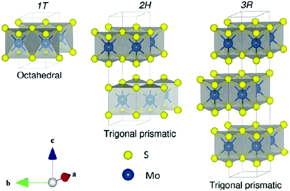
MoX2 compounds are composed of vertically stacked hexagonal layers of Mo covalently bonded to hexagonal layers of X atoms and these layers are held together by weak van der Waals forces. They are highly anisotropic, and it is reported that the conductivity values are around 100 times lower in the perpendicular direction than those in the MoS2 planes. A similar trend is observed for electrical properties. These materials exist in various polymorphic forms, mainly 2H and 1T. The trigonal prismatic coordination is observed in the 2H phase showing semiconducting properties, while in 1T the central atom is octahedrally coordinated, and it is metallic in nature. In a trigonal prismatic structure, the atoms’ packing is AbA type, while in an octahedral structure it is AbC type (capital letters denote chalcogen atoms and the lowercase letter denotes a metal atom).22 The 1T phase shows better activity in hydrogen evolution and energy storage than the 2H phase.23
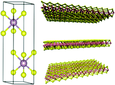
The Earth's crust contains MoS2 in the form of molybdenite. It exists in three polymorphic phases – 1T, 2H, and 3R belonging to point groups D6d, D6h and C3v, respectively. Here, the numerals 1, 2 and 3 indicate the numbers of layers and T, H, and R denote tetragonal, hexagonal, and rhombohedral structures, respectively. The crystal structure for all the three phases is depicted in Fig. 1.24 Naturally, MoS2 occurs in the 2H phase. Mo coordinates octahedrally in the 1T phase and exhibits paramagnetic behaviour. It transforms into a more stable form, i.e., 2H-MoS2, upon aging or heating e.g. when Guo et al.25 annealed 1T′-MoS2 to 300 °C in an Ar atmosphere, it transformed to 2H-MoS2 with stability up to ∼1200 °C, thereafter it is converted to Mo2S3. 3R-MoS2 has Mo in trigonal prismatic coordination and transforms to its 2H-prototype upon heating.10 Guo et al.25 reported a phase change by intercalation with alkali metal ions. This transformation is attributed to the change in the electronic structure from d2 to d3, which leads to destabilisation in the trigonal prismatic 2H phase and conversion to the octahedral 1T phase. The S–Mo–S layer-to-layer distance is about 6 Å.
 |
| | Fig. 1 Unit cell structure of various polymorphs of MoS2. Reprinted with permission from ref. 24 [A. Kuc, in Chemical Modelling: Volume 11, The Royal Society of Chemistry, 2015, vol. 11, pp. 1–29]. Copyright The Royal Society of Chemistry. | |
Similarly, MoSe2 is also found in the Earth's crust as a scarce mineral drysdallite. 2H-MoSe2 with the hP6 space group has cell parameters of a = 3.283 Å and c = 12.918 Å. The electron mobility is higher in 2D MoSe2 than that in 2D MoS2. Bond lengths of 2.528 Å for Mo–Se and about 3.293 Å for Se–Se make them better candidates for various applications. MoSe2 monolayers are thicker than MoS2 because of the large atomic radius of Se atoms.26Fig. 2 represents the crystal structure of MoSe2 which is analogous to that of MoS2.27
 |
| | Fig. 2 Crystal structure of 2H-MoSe2 Reprinted with permission from ref. 27 [S. Tongay, J. Zhou, C. Ataca, K. Lo, T. S. Matthews, J. Li, J. C. Grossman and J. Wu, Nano Lett., 2012, 12, 5576–5580]. Copyright 2012 American Chemical Society. | |
MoTe2 crystallises in two phases, i.e., 2H and 1T′, whose crystal structure is presented in Fig. 3.28 The 2H phase belongs to the hP6, P63/mmc space group with unit cell sizes of a = 3.519 Å and c = 13.946 Å. The 1T phase belongs to the mP12, P22/m space group with unit cell constants of a = 6.33 Å, b = 3.469 Å, and c = 13.86 Å. The unit cell sizes change with temperature due to thermal expansion as the energy gap between these phases is very low (40 meV).29 It is reported that the 2H-phase is slightly less stable, i.e., 815 °C and beyond that it changes to the more stable phase of 1T′ which is stable even beyond 900 °C.30 Due to the weak bonding between Mo and Te, its synthesis in one pure phase is highly challenging, thus limiting its exploration and applications. Therefore, it is desired to conduct research in materials like MoTe2 with rapid pace. The role of chemists therefore becomes more demanding to propose simpler methods for the synthesis of pure phase MoTe2.
 |
| | Fig. 3 Crystal structure of (a) monoclinic 1T′-MoTe2 and (b) hexagonal 2H-MoTe2 phases. Reprinted with permission from ref. 28 [J. C. McGlynn, T. Dankwort, L. Kienle, N. A. G. Bandeira, J. P. Fraser, E. K. Gibson, I. Cascallana-Matias, K. Kamaras, M. D. Symes, H. N. Miras and A. Y. Ganin, Nat. Commun., 2019, 10, 4916]. Copyright 2019, The Authors. | |
Electronic properties
On moving from bulk to nano-scale, MoX2 give rise to diversified properties due to their transformation from indirect to direct bandgap semiconductors. It is well known that upon particle size reduction the bandgap increases in semiconductor materials and MoX2 are no exception to that. The bandgap values of these materials in bulk and the nano range are summarised in Table 1. The bandgap for bulk MoS2 is about 1.2 eV which can reach up to 1.8 eV for nano-MoS2 and thus IR-active MoS2 can be converted to visible active, which makes it a potential photo-catalyst. Similarly, MoSe2 has been reported to attain a bandgap of 1.5 eV in the nano-regime, thus extending its scope in optoelectronic applications. Likewise, bulk 2H-MoTe2 has an indirect bandgap of 0.93 eV, whereas a direct bandgap of 1.1 eV is reported for monolayer 2H-MoTe2.31 This value is very close to that of Si, and hence it finds numerous applications in photonics. As the bandgap of MoTe2 lies in the infrared region, it can be used as an infrared detector. It is also reported that MoTe2 can exhibit a higher phonon mobility than MoS2 at room temperature.32
Table 1 Comparison of bandgap values at the nano- and bulk level
| MoX2 |
Bulk bandgap |
Bandgap in the nano-regime |
| MoS2 |
Indirect (Eg = 1.2 eV)33 |
Direct (Eg = 1.8 eV)34 |
| MoSe2 |
Indirect (Eg = 1.1 eV) |
Direct (Eg = 1.55 eV)27,35 |
| MoTe2 |
Indirect (Eg = 0.93 eV) |
Direct (Eg = 1.1 eV)29 |
The bandgap in MoX2 decreases gradually from 1.8 to 1.1 eV as the size of the chalcogen increases. Therefore, it also gives an opportunity to tune the bandgap using different concentrations of chalcogens.36–38 In MoX2, Mo is in the +4 oxidation state having a 4d2 valence electronic configuration. In a trigonal prismatic structure, the electrons are filled in the dz2 orbital and the transition from this orbital to the dx2-y2 and dxy orbitals makes it semiconducting in nature, while in octahedral coordination, the electrons are filled in the t2g orbital (as unpaired in dxy and dyz) which corresponds to the valence band in the electronic structure of the 1T phase (Fig. 4).22 This partially occupied valence band in the 1T phase is responsible for its semi-metallic nature.39 As the dz2 orbital has a slightly lower energy than the t2g orbital, the overall energy of electrons is lower for the 2H phase, making it thermodynamically more stable than the 1T phase. Additionally, the lone pairs of chalcogens terminate the edges of layers, giving them stability against reaction with environmental species.22
 |
| | Fig. 4 d-orbital splitting diagram in trigonal prismatic and octahedral coordination. | |
Synthesis
Several approaches are documented for the synthesis of nano-MoX2. As the MoX2 layers are linked together through van der Waals forces, these forces can easily be dealt with to obtain few/monolayers of these materials conveniently from the bulk forms. Some notable approaches for the synthesis of nano-MoX2 practiced by researchers are hydrothermal, solvothermal, thermal decomposition, ultrasonication, chemical vapour deposition, microwave, mechanical exfoliation and chemical exfoliation. These techniques result in a wide diversity of morphologies. The commonly used molybdenum precursors are molybdenum trioxide, ammonium heptamolybdate (AHM), and sodium molybdate and the synthesis methods are discussed one by one in the following sub-sections.
Hydrothermal method
The hydrothermal method is a technique used to carry out chemical reactions at high temperatures and pressures. A properly sealed vessel, generally a Teflon lined stainless-steel autoclave, is used. The precursors and chemical reagents are dissolved in water and kept in an autoclave at high temperatures for long durations. Hydrothermal synthesis of molybdenum dichalcogenides has been extensively reported. Li et al.40 successfully synthesized MoS2 nanowires via a hydrothermal method. Prabhakar et al.41 synthesised MoS2 nanoflowers and nanosheets of less than 100 nm diameter and 10–50 nm thickness by the reaction of AHM with thioacetamide and thiourea, respectively, and using citric acid as a surfactant. The sulphur source was added to a moderately acidic aqueous solution of AHM and citric acid and then kept in an autoclave for about 10 h at 160 °C to collect a black powder. Similarly, by use of an autoclave, Tian et al.42 reported a green protocol for synthesis of MoS2 fine crystals using Na2MoO4 and potassium thiocyanate (KSCN) as precursors sealed in a stainless-steel autoclave at 260 °C for 24 h. They reported silvery dark crystalline nanosheets with a size of 0.3 μm from transmission electron microscopy (TEM) images. The suggested reaction is represented by eqn (1):| | | 4MoO2−4 + 9SCN− + 15H2O → 4MoS2 + SO2−4 + 3NH+4 + 9CO2−3 + 6NH3 | (1) |
Nagaraju et al.43 prepared bundles of MoS2 nanofibres via two different routes using AHM as the molybdenum precursor and sodium sulfide or H2S gas as the source of sulfur in the presence of citric acid as a surfactant. These reaction mixtures were sealed in an autoclave and kept at 180 °C for 48 and 24 h, respectively, depending on the source of sulfur. It is reported that, irrespective of the source of sulfur, the products from both the reactions have similar morphology, with the diameter of nanorods being about 150–300 nm and length being 20–25 μm based on scanning electron microscopy (SEM) images. It was demonstrated that the role of citric acid is very crucial to avoid the formation aggregates and impurities of MoO3. The reaction in the presence of citric acid is represented by eqn (2) and (3) showing that (NH4)2MoSO4 is formed as an intermediate.
| | | NH4MoO4 + 4Na2S + C6H8O7 → (NH4)2MoS4 + Na7C6H4O7 + 4NaOH | (2) |
| | | (NH4)2MoS4 → MoS2 + N2 + 2H2 + 2H2S | (3) |
Pourabbas et al.44 compared the formation of nano-ribbons of nano-MoS2via two different methods where, in the first case, MoO3 was mixed with Na2S in water and autoclaved for 12 h at 300 °C to isolate large poly-disperse particles with a size in the range of 150–200 nm composed of nanoribbons of 2–3 nm thickness and about 100 nm length. However, a better size domain was obtained when the authors dispersed AHM and thiourea in water with 1-octanol and sodium lauryl sulphate as surfactants, sealed them in an autoclave at 180 °C for 5 h and obtained particles in the size range of 20–30 nm in the form of ribbons with uniform distribution. Synthesis of relatively small particles of 3R-MoS2 with a mean diameter of about 5.5 nm was reported by Manuja et al.45 by autoclaving the aq. mixture of Na2MoO4, polyethylene glycol (PEG) and thiourea at 200 °C for 11 h. Hou et al.46 synthesised spherical and flower-like MoS2 nanoparticles by modifying the additive used such as CTAC, PEG and ethyl alcohol in the reaction of sodium molybdate and thioacetamide. Sodium molybdate and thioacetamide were taken in the stoichiometric ratio, and then the additive was added with some amount of water. They further acidified the mixture to set the pH to 1 and the mixture was then sealed in an autoclave and heated in a muffle furnace for 6 h at 220 °C. The course of the reaction is represented by eqn (4)–(9). The authors found that spherical nanoparticles were obtained using CTAC and PEG as additives with little difference in their sizes, whereas flower-like MoS2 NPs were obtained using ethanol.
| | | CH3CSNH2 + 2H2O → CH3CONH4 + H2S | (4) |
| | | Na2MoO4 + 4H2S → Na2MoS4 + 4H2O | (5) |
| | | Na2MoS4 + 4HCl → H2MoS4 + 2NaCl | (6) |
| | | Na2MoS4 + H2SO4 → H2MoS4 + Na2SO4 | (7) |
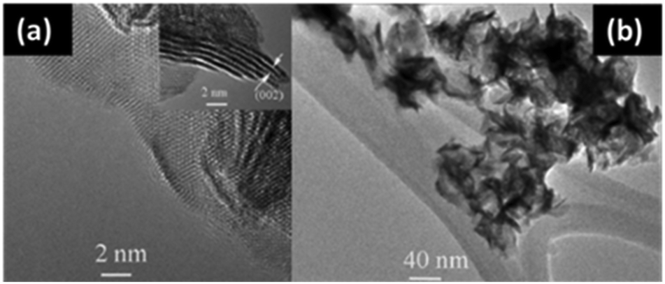
Similarly, there is an extensive use of the hydrothermal method for the synthesis of nanocrystalline MoSe2.47–51 Common selenium precursors often employed are Se and Na2SeO3. Several researchers described excellent use of the hydrothermal method to obtain MoSe2, e.g. the mixture of Na2MoO4, hydrazine hydrate/L-ascorbic acid and Se in distilled water can be processed in an autoclave for several hours at 200 °C to obtain flower-like morphology made up of very thin nanosheets,14,52 as supported by high resolution transmission electron microscopy (HRTEM) images (Fig. 5).
 |
| | Fig. 5 HRTEM image of MoSe2 prepared by a hydrothermal method. Reprinted with permission from ref. 52 [H. Tang, K. Dou, C.-C. Kaun, Q. Kuang and S. Yang, J. Mater. Chem. A, 2014, 2, 360–364.]. Copyright The Royal Society of Chemistry. | |
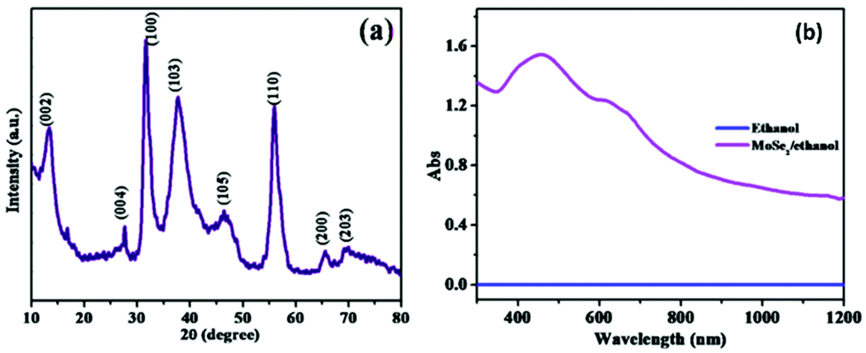
The typical XRD and UV absorption spectra of MoSe2 formed by this method are shown in Fig. 6.14 The XRD results supported that the 2H phase was formed and the absorption was observed at ∼ 450 nm and ∼650 nm, indicating that the thus-formed compound is a useful photo-sensor in the range of 400–700 nm. Modifications and alterations are often performed by different groups to enhance the product yield as well as the properties for making them suitable for a variety of applications. In one such modification, a pH-based synthesis has been explored by Mittal et al.53 to study its impact on the size and morphology of MoSe2. Nanosheets and nano-urchins that contained several nanospheres were obtained at pH 5 and pH 8, respectively, via a three-step mechanism. In the first step, hydrazine hydrate reduced selenium to give selenium ions as per eqn (10). When this solution was added to a solution of sodium molybdate in water, excess hydrazine hydrate reduced Mo6+ ions in Na2MoO4 to Mo4+ ions (eqn (11)). Finally, the product was formed as per eqn (12) where the reaction between molybdenum and selenium ions took place in an autoclave.
| | | 5N2H4 + 2Se → N2 + 4N2H+5 + 2Se2− | (10) |
| | | 2MoO2−4 + N2H4 + 4H2O → 2Mo4+ + N2 + 12OH− | (11) |
 |
| | Fig. 6 XRD and UV-Vis spectra of 2H-MoSe2. Reprinted with permission from ref. 10 [N. T. Shelke and D. J. Late, Sens. Actuators, A, 2019, 295, 160–168]. Copyright 2019, Elsevier. | |
In similar efforts, Xiao et al.54 used sodium molybdate and selenium powder with various amounts of basic reducing agent such as NaBH4 to synthesize MoSe2 in mixed 1T and 2H phases where it has been described that by increasing the amount of NaBH4, the number of stacked layers can be decreased. Likewise, MoSe2 nanorods and spherical particles were synthesized by Ghritlahre et al.55 using a basic aq. solution of sodium molybdate or AHM as the molybdenum precursor and Se powder with a small amount of hydrazine hydrate (HH) in an autoclave at 200 °C.
Often it is realized that the source of selenium is a tricky choice and it is crucial for the preparation of the product of desired morphology and physical properties. Thus, researchers constantly explore a variety of such combinations and look for newer, unexplored and more appropriate selenium precursors to suit the metal precursors for establishing the appropriate kinetics. Inorganic selenium precursors may offer more versatility in surface properties when compared with selenium metal as a source. Setayeshgar et al.56 were the first to use sodium selenite as the selenium source for the synthesis of nanocrystalline MoSe2. This eliminated the requirement of any reducing agent like hydrazine hydrate as Na2SeO3 readily dissociates in water to give Se2− ions. They proposed that the reaction of MoCl5/NaOH/ethylene glycol and Na2SeO3 can yield bi-phase 1T, 3.5-to-6 nm thick 2H-MoSe2 nanosheets of 5 to 8 layers via autoclave heating at 200 °C for 18 h. The fine tuning of the size and morphology was reported by varying the ratio of reagents and precursors. The suggested chemical reactions in this process are represented by eqn (13) and (14).
| | | 2MoCl5 + 8NaOH → 2Mo(OH)4 + 8NaCl + Cl2 | (13) |
| | | 2Na2SeO3 + Mo(OH)4 + NaCl + H2O → MoSe2 + 5NaOH + HCl + 3O2 | (14) |
It is noticed that MoCl5 was reduced to Mo4+ in the first stage, followed by in situ release of Se2− from Na2SeO3. In another study, Liu et al.57 used potassium selenocyanate as the selenium source with AHM in the water/ethylene glycol (EG) mixture and synthesized MoSe2 microspheres consisting of MoSe2 nanosheets. According to them, potassium selenocyanate dissociates to give H2Se in the reaction as per eqn (15) which reacts with Mo4+ ions produced in the mixture to give MoSe2.
| | | NCSeCH2COO− + H+ →CO2 + NH3 + H2Se | (15) |
With set methodologies for sulphides and selenides, counterpart tellurides have not been much explored but still there are a few reports on its hydrothermal synthesis, e.g. Li and co-workers58 synthesized MoTe2 nanosheets having thickness in the range of 20–80 nm. Te powder was mixed with water in the presence of NaBH4, followed by addition of sodium molybdate with continuous stirring and heating. The mixture was then transferred to an autoclave and maintained at 200 °C for 48 h. Diffraction peaks at 12.66° (002), 25.48° (004), 29.9° (100), 29.99° (101), 35.17° (103), 43.93° (105), 51.94° (110), 52.33° (008) and 64.28° (203) were seen in the XRD spectrum of 2H-MoTe2. Although the method offers easy processing and a green alternative, products of uncertain/mixed morphology are obtained.
Solvothermal method
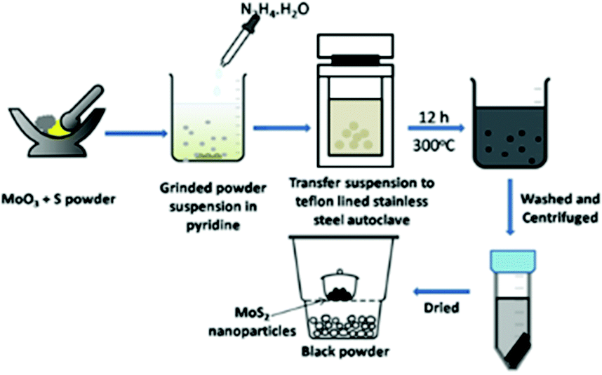
Solvothermal and hydrothermal methods are analogues, except that the organic solvents are used instead of water for the synthesis. The precursor and solvent mixture are sealed in a vessel and the reaction is carried out at a temperature more than the boiling point of the solvent. The Mo–chalcogenide synthesis reactions require a very high temperature/energy as the precursors like MoO3 and chalcogen sources often do not break/dissociate easily at normal temperatures. In such a situation solvothermal methods for synthesis of nanomaterials are considered very handy to obtain uniform sized particles. Zhan et al.59 synthesised uniform thin platelets of MoS2 (100 nm thickness) from MoO3 and elemental sulphur using hydrazine in pyridine in an autoclave that was maintained at 300 °C for 12 h. They proposed that, firstly, MoO3 may be reduced to MoO2 by hydrazine hydrate and, on the addition of sulphur powder, O-atoms are replaced by S-atoms to form MoS2 nanoparticles (NPs). The reaction methodology is depicted in Fig. 7.
 |
| | Fig. 7 Preparation of MoS2 NPs in an autoclave using MoO3 (ref. 59). | |
Similarly, Li et al.60 mentioned the synthesis of free MoS2 in a single step where (NH4)2MoS4 and N2H4·H2O were mixed in DMF and heated in a Teflon-lined autoclave at 200 °C for 10 h. They, initially, synthesized MoS2 particles on graphene and elaborated that even without graphene free standing MoS2 can be prepared from this method. Such an approach was found to be useful for catalytic applications. The formation of a colloidal solution of MoS2 nanosheets was reported by Zhu et al.61 from micro MoS2 powder dispersed in n-hexane and reacted with n-butyllithium (n-BuLi) in an autoclave for 5 h at 100 °C. The MoS2 nanosheets were obtained via repetitive washing of the intermediate compound LixMoS2, followed by its hydrolysis by sonication for 1 h in water. Similarly, flower like nanoparticles composed of ultrathin nanosheets of MoS2 have been reported by use of the sodium molybdate, thiourea and hydroxylamine hydrochloride mixture (1![[thin space (1/6-em)]](https://www.rsc.org/images/entities/char_2009.gif) :2:2 molar ratio) in an autoclave heated for 24 h at 190 °C, followed by annealing for 5 h at 500 °C.62 The authors observed that a lower temperature and reaction time leads to formation of MoO2 impurities.
:2:2 molar ratio) in an autoclave heated for 24 h at 190 °C, followed by annealing for 5 h at 500 °C.62 The authors observed that a lower temperature and reaction time leads to formation of MoO2 impurities.
Several researchers have also reported synthesis of nano-MoSe2 by the solvothermal method using an autoclave. The synthesis method is very much similar to that of MoS2 where only the sulphur source is replaced by a selenium source. The most commonly used precursors are MoO3 and Se powder with some reducing agents like N2H4·H2O.63 Jiang et al.64 suggested that the thickness of MoSe2 nanosheets can be decreased with increasing carbon chains in alcohol when performing the synthesis using various solvents like ethanol, butanol, hexanol and octanol. They also commented on the morphology with respect to the reaction temperature. The particles formed at 120 °C were spherical in shape with no clear evidence of nanosheets. When the temperature was increased, nanoflowers composed of thin nanosheets were observed; with further increase in temperature, these nanosheets became thicker.
Despite the popularity of the solvothermal method, it has limitations for high melting solids which have poor or no solubility. Therefore, compounds like MoTe2 have not been popularly synthesized by this method unlike by the hydrothermal method where synthesis of MoTe2 nanosheets has been possible with ease via in situ reduction of Te powder by NaBH4 which is useful in generating Te2− ions. Similarly, the reaction medium in the solvothermal method may have its utility for MoTe2 formation. It is challenging, however, to monitor the pressure during the synthesis and the nature of solvents versus the duration/pressure may limit its operational understanding.
Thermal method
The generally adopted methods are mostly based on the autoclave requirement which requires special skills to operate and, hence, is highly challenging. It is always desirable that simpler methods be developed for enhancement of the applicability of materials with ease. In this regard, direct reactions in standard laboratory glassware are generally favourable and preferred. The thermal method, therefore, being the most conventional, brings its own advantages. By this method, researchers can monitor the reaction changes physically as well as spectroscopically at desired time intervals during the course of reactions. The precursors in such methods are solvent-friendly in terms of dispersion/solubility. Some of the popular reagents are metal complexes, molecular precursors and/or chalcogen sources which react at normal pressure and at a temperature below 300 °C. There are a number of reports where soft solution methods have been practiced. For example, Duphil et al.65 synthesised MoS2 by thermal decomposition of Mo(CO)6. The sulphur powder was dissolved in p-xylene by heating, followed by the addition of Mo(CO)6 at room temperature and refluxing at 140 °C for several hours. The reaction setup is shown in Fig. 8. Raman spectroscopy was extensively and effectively applied for monitoring the reaction by way of disappearance of the CO peak as the formation of a black precipitate starts. It was opined that Mo(CO)6 decomposed to give elemental Mo, followed by its reaction with the S present to give a black precipitate of MoS2 of 10–30 nm size albeit not without aggregation. The overall reaction is represented by eqn (16):| | | Mo(CO)6 + 2S → MoS2 + 6CO | (16) |
 |
| | Fig. 8 Reaction between Mo(CO)6 and S under a nitrogen atmosphere to synthesise MoS2 NPs.65 | |
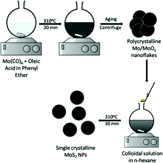
Park et al.66 reported preparation of MoS2via generation of a colloidal solution of Mo NPs, followed by its reaction with sulphur via a thermal method. In this method, Mo(CO)6 and S were reacted in the presence of oleic acid to control the particle size. The reaction consists of two steps – (1) formation of polycrystalline Mo/MoOx nanoflakes and (2) reaction with sulphur to produce MoS2. By this method, highly crystalline and spherical MoS2 NPs of about ∼2 nm size were obtained. The schematic illustration is shown in Fig. 9.
 |
| | Fig. 9 Synthesis of ultra-small MoS2 NPs using oleic acid.66 | |
It is well documented and understood by this time that chemical methods can produce high quality nanostructured materials and the challenges associated with their synthesis can be addressed by chemists via skill manipulation. Often temperatures less than 300 °C are appropriate to operate in a Schlenk system in an advanced chemistry laboratory and the solvents and precursors can be degassed prior to or during an in situ stage. Sun et al.67 and Wang et al.68 dissolved Se powder in 1-octadecene (ODE) by heating and stirring it. The mixture of sodium molybdate, oleic acid (OLA) and octylamine was heated in an Ar atmosphere to obtain a red-brown solution. Later, they added ODE–Se solution to it and heated at ∼300 °C for about half an hour. The SEM/EDAX and TEM analyses of the black powder so obtained revealed formation of MoSe2 nanoflowers consisting of nanosheets. Similarly, Zhang et al.69 prepared a stock solution of Se in ODE and OLA. Sodium molybdate was dissolved in ODE and OLA and heated to 300 °C. The authors observed a colour change from light yellow to light brown and finally a clear dark brown solution. Subsequent addition of Se–ODE/Se–OLA solutions resulted in a black precipitate of nano-MoSe2 clusters with a size of ∼250 nm composed of ultrathin nanosheets as shown in the TEM images. EDAX analysis showed that these nanostructures were slightly Mo-rich. In a similar manner, Guo et al.70 dissolved Mo(CO)6 in oleylamine (OAm) to which they added Se–ODE precursor and heated the mixture at 200 °C for about half an hour. This way, ultrathin nanosheets of 2H-MoSe2 were reported. Huang et al.71 synthesised MoSe2 nanoclusters having a particle diameter in the range of 3.5–6 nm. Synthesis employing chloride of molybdenum may however be really tricky and painstaking. The reaction takes a much longer time and thus increases the challenges for researchers. MoCl5 was refluxed for three days in tetrachloroethylene in an inert atmosphere for reduction of MoCl5 to MoCl4. Subsequently, dissolving it in an inverse micelle solution of tri-dodecyl methylammonium iodide, hexanol and octane and combining with H2Se yielded nanoclustered MoSe2. It should be noticed that the use of H2Se is not so convenient. To make the synthesis simpler, researchers have explored the use of organo-selenium compounds as sources of selenium which avoids difficulties associated with the first stage of reaction where selenium precursors are generated in situ. Accordingly, Geng et al.72 employed MoO2(acac)2 and (PhCH2)2Se2 as precursors and OAm as the surfactant to synthesize MoSe2 nanosheets. Thermally heating the mixture to ∼250 °C yielded a black precipitate of thin sheet MoSe2. Varied layers of MoSe2 nanosheets were synthesized conveniently by Hassan et al.73 by increasing the amount of surfactant during their experiment involving the use of MoO2(acac)2 in OAm, followed by heating with Se-precursor (prepared by stirring Se powder, OAm and 1-butanethiol) under an inert atmosphere. It was described that the reaction occurs via reduction of Se to Se2− ions.
In line with MoSe2, thermal methods are also effectively useful for synthesis of its tellurium counterpart. Thus, Sun et al.74 were able to synthesize 1T′-MoTe2via a low-temperature thermal route by using TOPTe prepared by dissolution of Te powder in trioctylphosphine (TOP) and OAm by heating to obtain a yellow solution. Subsequent injection of hexamethyldisilazane along with MoCl5 solution in OLA led to formation of a nanocrystalline product within half an hour at 300 °C. OLA was used as the complexing agent and OAm as the reducing reagent and HDMS was required for high crystallinity. 1T′-MoTe2 nanoflowers were formed directly at this temperature instead of the more preferred and stable 2H polymorph. The authors suggested that this could be due to the low energy barrier for the 1T′ phase by the organic ligands. Qiu et al.75 carried out a reaction between Mo(CO)6 and Te powder in diphenylmethane by heating it for 24 h in a N2 atmosphere. It was then annealed at 650 °C for 4 h to obtain MoTe2 in a stoichiometric ratio. They observed that excess of Te was present in the sample before annealing. According to them, this was probably due to faster sublimation of Mo(CO)6 and deposition of MoTe2 particles over Te powder. SEM and TEM images indicated mixed morphologies in the form of nanorods and nanosheets. Liu et al.76 synthesized nanosheets of 1T′-MoTe2 with lateral dimensions of 250–350 nm and about 4 nm thickness. Te was first dissolved in TOP, then injected into Mo(CO)6 dispersed in OAm and heated at more than 300 °C for 2 h. When the same experiment was repeated using MoCl5, spherical nanostructures with smaller dimensions composed of defect rich nanosheets were observed. This states that different precursors can have different effects on the product morphology.
Chemical vapour deposition
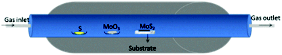
Solid-state reactions mostly use MoO3, sulphur, hydrogen, H2S, etc. as precursors for the synthesis of nano-MoS2 utilizing a high temperature tube furnace.77–79 The temperature required to carry out solid-state reactions is very high to realize high yields and homogeneous quality, and to have precise control over layer numbers. CVD grown layers are prone to chalcogenide deficiency due to the volatile nature of chalcogens. Balendhran et al.80 carried out a solid-state reaction between MoO3 and S powder in a tube furnace which they referred to as the thermal evaporation technique using a quartz substrate in an argon environment. The reaction methodology for the same is shown in Fig. 10. It was demonstrated that layered MoS2 deposition can be achieved via choosing the right combination of temperatures and durations. Highly crystalline and ordered layered structures were reported at an annealing temperature of 830 °C for 3 h. The suggested reaction mechanism is represented by eqn (17) and (18):| | | 2MoO3 + S → 2MoO2 + SO2 | (17) |
| | | 2MoO2 + S → 2MoO2 + SO2 | (18) |
 |
| | Fig. 10 Experimental setup for the reaction carried out in a tube furnace.80 | |
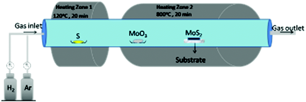
On the same line, Jeon and co-workers81 synthesised monolayered MoS2 with a controlled size of nanoparticles in the range of 5–60 nm by regulating the flow of hydrogen and argon. Here, they used a dual temperature zone furnace to carry out the reaction where sulphur powder was placed in the first zone and MoO3 powder and the silicon substrate were placed next to each other in the second zone. Instead of one heating zone, two were preferred as sulphur is highly volatile than MoO3, and to cause their evaporation at the same time, it is required to heat them at different temperatures. Otherwise, the product would be S-deficient as reported by several researchers where the reaction was carried out in a single zone. The setup of the reaction is shown in Fig. 11. The first zone was heated at 120 °C and the second zone at 800 °C for 20 minutes with the ratio of Ar/H2 well-regulated as required. The authors observed that the size of the nanoparticles can be reduced with increasing the H2 flow rate. It is also worth mentioning that a typical MoS2 stoichiometry was obtained when no hydrogen was used which the authors suggested could be due to the possible reduction of S, leading to substantial loss of sulphur during sulfurization of Mo. When MoS2 is formed, the edges are covered by S dimers. As the flow of H2 increases, it acts as the reducing agent and reacts with these surface-attached dimers to form H2S. Therefore, instead of pure MoS2, partially reduced MoO3-xS is deposited. The proposed reaction is represented by eqn (19) and (20):
| | | MoO3 + 3S + H2 → MoO3−xS + SOx + H2 | (20) |
 |
| | Fig. 11 Schematic diagram of the CVD system used to synthesise various sized MoS2 nanoparticles by regulating the flow of gases.81 | |
Reacting MoO3 nanobelts with sulphur powder, Li et al.82 synthesised MoS2 fullerenes. The reaction was performed in a tube furnace in an inert atmosphere of argon gas at a temperature higher than 800 °C.
Based on TEM analysis, the authors stated that nanotubes of MoS2 as well as fullerene-like nanoparticles were formed by rolling of the layered structures. It is also evident from this article that the morphology of products is dependent on the morphology of the reactants. When the authors carried out the same reaction with micro MoO3, nanoparticles of MoS2 were formed instead of nanotubes. In an attempt to identify whether the formation of MoS2 nanotubes from the reaction of MoO3 with H2S gas takes place through the MoS3 intermediate,83 Nath et al.84 reported conversion of MoS3 obtained by decomposition of ammonium thiomolybdate to MoS2 nanotubes via heating it above 1200 °C in a hydrogen stream. Direct heating of ammonium thiomolybdate also yielded MoS2 nanotubes. This indicates that MoS3 is the intermediate in the formation of nanotubes. The reduction of ammonium thiomolybdate with hydrogen to produce MoS2via the MoS3 intermediate is shown by eqn (21) and (22):
| | | (NH4)2MoS4 → MoS3 + H2S + NH3 | (21) |
| | | MoS3 + H2 → MoS2 + H2S | (22) |
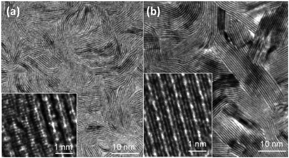
Kong et al.7 presented synthesis of thin MoS2 and MoSe2 layers vertically aligned on a substrate so as to achieve maximum catalytic activity. They obtained samples with an excellent arrangement of the layers as shown in the HRTEM images (Fig. 12). Recently, the use of KCl to obtain mixed phase MoS2 heterostructures was also reported.85
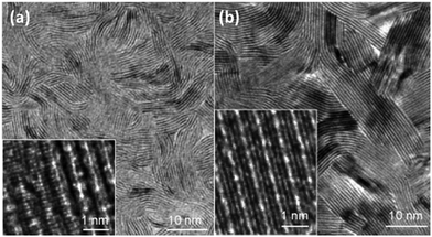 |
| | Fig. 12 TEM and the corresponding HRTEM (inset) images of (a) MoS2 and (b) MoSe2 depicting uniformly spaced and vertically aligned layers. Reprinted with permission from ref. 7 [D. Kong, H. Wang, J. J. Cha, M. Pasta, K. J. Koski, J. Yao and Y. Cui, Nano Lett., 2013, 13, 1341–1347]. Copyright 2013, American Chemical Society. | |
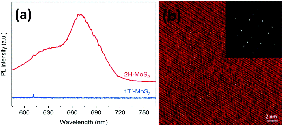
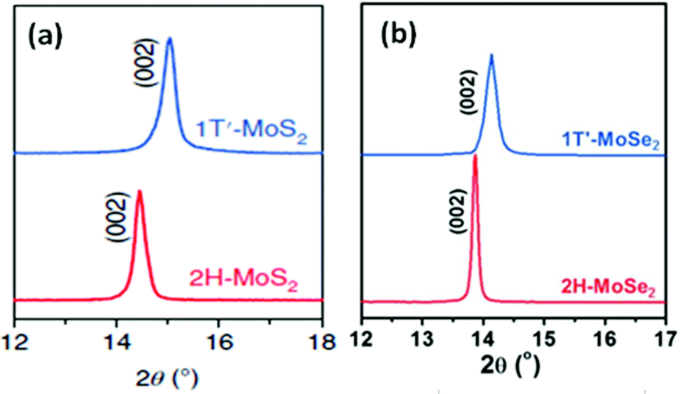
Lee et al.86 prepared thin MoS2 layers of ∼0.72 nm thickness and more than 150 nm in lateral dimensions over an RGO coated Si/SiO2 substrate via chemical vapour deposition taking MoO3 and sulphur powder as precursors. The authors observed two prominent peaks at 627 and 677 nm in their PL spectra due to A1 and B1 direct excitonic transitions. Wypych et al.87 carried out the reaction of potassium molybdate and H2S by heating it for almost 24 h in the temperature range of 300–400 °C, followed by reduction in a H2/N2 atmosphere at a much elevated temperature (850 °C) for 3 days to form KMoS2. After hydration and oxidation of KMoS2, 1T′ MoS2 was formed. The process took a very long time, and the product too contained some impurities. Modifying this process, Yu et al.23 were successful to synthesise pure 1T′-MoS2 crystals. After grinding K2MoO4 and S powder together, the mixture was annealed for 1.5 h at 450 °C under a H2/Ar flow. Excess S was added to the obtained powder and again annealed for 10 h at 850 °C with increased H2 flow, followed by soaking and washing with DI water. Later, it was soaked for a few hours in I2/acetonitrile solution and dried after washing thoroughly with DI water to achieve 1T′-MoS2 crystals. Replacing S with Se in this process, 1T′-MoSe2 was prepared. Annealing 1T′-MoS2 and 1T′-MoSe2 at 200 °C produced 2H-MoS2 and 2H-MoSe2, respectively.
The higher negative reduction potential of Se poses greater challenges in the synthesis of MoSe2 when compared with MoS2.88 Most reports on the synthesis of MoSe2 layers use the CVD method in a very similar manner to the synthesis of MoS2. Often selenization of MoO3 with Se is a popular methodology to generate MoSe2. It was demonstrated that Ar and N2 are good carrier gases to maintain an inert atmosphere with some percentage of H2 for facilitating reduction.89–91 Shaw et al.92 synthesised large triangular MoSe2 monolayers having edge lengths up to 30 μm and heights up to 1 nm. The operating temperature of the furnace was kept at 750 °C for 15 minutes during which the zone containing Se powder was maintained at ∼300 °C to avoid faster vaporization of Se. Using the same method, Huang et al.5 synthesised snow-like single crystal MoSe2 with a hexagonal structure by use of Se and MoO3 and placing a Si/SiO2 substrate inverted over Se in a three-zone tube furnace. The reaction was carried out in an Ar/H2 atmosphere, heating Se at 520 °C and MoO3 at 820 °C for half an hour. Depending upon the gas flow rate, large triangular monolayers of lateral dimensions close to 20 μm and snow-like monolayers of 0.9 nm thickness were formed. The PL peak was observed at 814 nm corresponding to a 1.52 eV bandgap. The 2H-phase was confirmed from the SAED pattern and the d-spacing calculated matched [110] and [100] crystal planes.
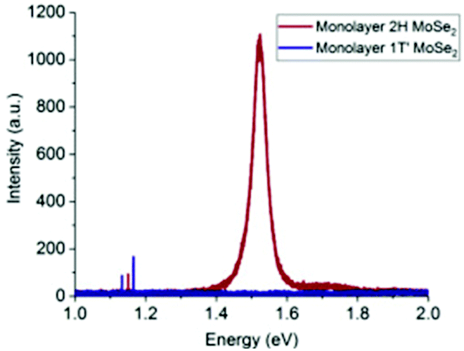
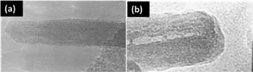
Hanson et al.93 transformed MoSe2 from 2H to 1T′ via exposure to n-BuLi. They first synthesized 2H-MoSe2 monolayers by the above-described CVD method by heating MoO3 and Se powder at 800 °C. The chips were treated with n-BuLi solution in hexane for 12 h in an Ar atmosphere. Various characterization studies supported the successful formation of the 1T′-MoSe2 monolayer. The PL spectra (Fig. 13) gave a bandgap value of ∼1.5 eV for 2H-MoSe2, while no photoluminescence was observed for 1T′-MoSe2. Taking pointers from the synthesis of MoS2 by reduction of the corresponding trisulphide,84 Nath et al.94 were successful in synthesizing MoSe2 nanotubes in a similar manner. In addition, MoSe2 nanotubes via decomposition of (NH4)2MoSe4 in a reducing H2 atmosphere were also successfully synthesized. The reaction involved is represented by eqn (23). The morphology of the products was analysed through TEM (Fig. 14).
| | | (NH4)2MoSe4 + H2 → MoSe2 + 2H2Se + 2NH3 | (23) |
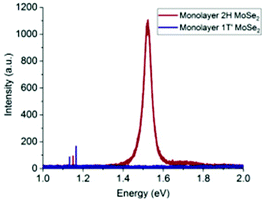 |
| | Fig. 13 PL spectra of monolayer 2H and 1T′-MoSe2. Reprinted with permission from ref. 93 [E. D. Hanson, L. M. Lilley, J. D. Cain, S. Hao, E. Palacios, K. Aydin, C. Wolverton, T. Meade and V. P. Dravid, Mater. Chem. Phys., 2019, 225, 219–226]. Copyright 2019, Elsevier. | |
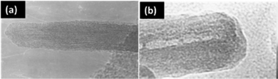 |
| | Fig. 14 MoSe2 nanotubes obtained via decomposition of (a) MoSe3 and (b) (NH4)2MoSe4. Reprinted with permission from ref. 94 [M. Nath and C. N. Rao, Chem. Commun., 2001, 2236–2237.]. Copyright The Royal Society of Chemistry. | |
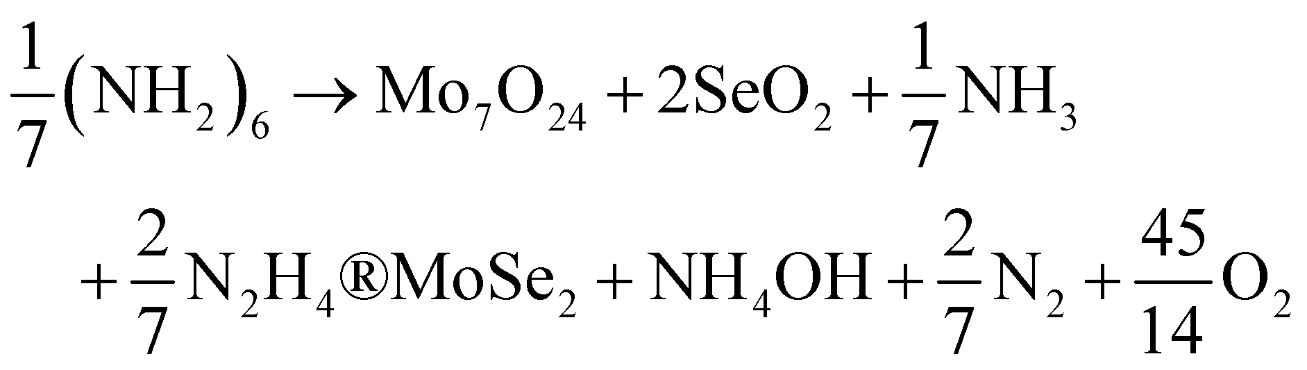
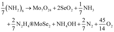
Vikraman et al.95 used a chemical bath deposition method to deposit MoSe2 on the substrate and post-annealing at 450 °C for an hour. The bath solution in which the substrate was dipped contained AHM, SeO2, N2H4, and NH3 solution with a certain amount of HCl. They represented the overall reaction by eqn (24). The authors observed that with an increase in the deposition time, the thickness of the layers increased as expected. It was also noticed that the layers align vertically till the deposition time reached 15 minutes, and beyond that there was a random alignment of layers.
| |  | (24) |
Gas phase reactions to synthesise MoTe2 are not easily achievable as a consequence of a lower bonding energy between Mo and Te or the requirement of high temperatures and longer durations to react. Moreover, at higher temperatures, instead of forming MoTe2 vapours, it loses Te as vapours leading to Te deficiency in the prepared MoTe2 samples. The MoTe2 layers being prone to oxidation are often coated with a protective layer of materials such as aluminium, polymethylmethacrylate (PMMA), silica, etc. Therefore, the synthesis of few-layer MoTe2 is highly challenging. The melting point of Te is about 450 °C. A large number of articles have reported the use of the CVD method for MoTe2 synthesis.28,96–98 Huang et al.31 used the physical vapour deposition technique to produce 3L 2H-MoTe2. MoTe2 was deposited on a silica substrate from a MoTe2 target for half a minute at 400 °C in an inert environment using a DC magnetron sputtering system. Then, the sample was annealed for several hours at 650 °C in a N2 atmosphere after coating it with a protective layer of silica, in an attempt to avoid decomposition of MoTe2. The 1T′ phase transformed to the 2H phase post-annealing and the cross-sectional HRTEM image of MoTe2 showed a three-layer stacked 2H-MoS2 structure with 2.1 nm thickness.
Zhou et al.99 and Hussain et al.100 synthesised MoTe2via tellurization of MoO3 and Mo films. Mo film was deposited on a SiO2 substrate and converted to MoO3via oxidation in air. It was then placed over Te powder in a CVD chamber in a reducing environment of Ar/H2 at 700 °C. Large nanosheets of ∼30 μm lateral size were observed. The authors also mentioned that when a Mo film was used instead of the MoO3 film, the 1T′ phase was obtained. In place of depositing the MoO3 film directly from MoO3 powder, the authors oxidised a Mo film to form MoO3 because MoO3 has a tendency to lose oxygen during evaporation. Similarly, in another experiment MoO3, MoCl5 and Te were taken in a 1:1:1 weight ratio and heated in a tube furnace at 780 °C for nearly 15 minutes, resulting in formation of 1T’-MoTe2 monolayers.101 Shirpay et al.102 deposited nanosheets of 2H-MoTe2via the chemical vapour transport method using MoO3 and TeO2. Kim and co-workers103 were able to synthesize ultrathin MoTe2 mixed phase films with a thickness of about 1–2 nm at a lower temperature using the Mo(CO)6 complex and dibutyl telluride as the precursors. Pradhan et al.104 synthesized bi-layered MoTe2 crystals on a silica substrate using iodine as the transport agent. As starting materials, they utilized Mo and Te powders, which required a very high temperature (∼1100 °C) and a very long duration (1.5 weeks) to react. Yang et al.105 controlled the MoTe2 nanosheet phases by optimizing the flow of the carrier gas employed and the tellurization temperature. The synthesis was carried out in a two-zone CVD chamber using MoO3 and Te to obtain thin films with thickness around 4 nm. The four stages observed were the 2H phase dominant coexistence of both phases, pure 2H phase, 1T′ phase dominant coexistence of both phases and phase pure 1T′-MoTe2. They observed that when the flow rate of N2 was increased from 1 sccm (standard cubic centimeters per minute) to 40 sccm, the 1T′ dominant phase was transformed to the 2H dominant phase with phase pure 2H-MoTe2 at 3 sccm and 1T′-MoTe2 at approximately 90 sccm. The dependence of phase on the synthesis temperature was also studied and the authors suggested that achieving 100% pure 2H-MoTe2 was highly unapproachable, while a pure 1T′ phase can be easily obtained with a high rate of tellurization. In a similar attempt to utilize MoTe2 as a phase change material, Empante et al.106 obtained 1T, 1T′ and 2H phases by varying the cooling rate of the furnace after the reaction. They carried out a reaction between MoO3 and Te in a CVD chamber for about 30 min at 650 °C for the 2H phase and at 680 °C for the other two phases. 1T, 1T′ and 2H phases were obtained when the chamber was opened after the temperature reached below 450 °C, 350 °C and 100 °C, respectively. This suggested that the 2H-phase is favoured at lower temperatures and an increase in temperature maximises the probability of 1T-MoTe2 formation.
In CVD, the film quality, i.e., the dimensions and the stoichiometry, is dependent on the amount of solid precursors, the distance at which they are placed, the substrate and its position, growth temperature and duration. The cooling rates of the sample also determine the phase of MoX2 compounds.
Microwave method
Microwave radiation causes direct and targeted heating of the sample with a minimum dissipation of energy in the surrounding. The use of microwave transparent glassware minimises the loss of energy to heat the sample container. Under microwave irradiation, solvents are superheated. As a result of this overheating, metal ions may reduce to a zerovalent state. Metal particles strongly interact with microwave irradiation, yielding very favourable reduction conditions. Microwave energy is more intense as compared to thermal heating and also there is targeted heating of the reaction mixture, thereby avoiding the energy wastage in heating a higher quantity of solvent and the reaction vessel which is generally the case in thermal heating. Therefore, microwave reactions are more efficient and less time-consuming. Qureshi et al.107 synthesised biocompatible and non-cytotoxic MoS2 by a microwave-assisted solvothermal method. AHM and elemental sulfur were taken in a 1:1 ratio in water, followed by addition of hydrazine monohydrate, for initial reaction activation. The reaction mixture was then irradiated with microwave radiation for 10 min at 270 W and the black precipitate suggested the formation of MoS2. The authors observed the morphology of NPs to be elongated rod-shaped from TEM images, and the SEM images show stacked plate-like structures. The reaction schematic is shown in Fig. 15.
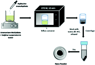 |
| | Fig. 15 Microwave synthesis of rod-shaped MoS2 NPs.107 | |
The polyol method is a potentially useful approach for the synthesis of metal NPs. Polyol serves as a reducing agent as well as a surface protecting agent. Harpeness et al.108 utilised this method to synthesise MoSe2 nanorods using a household microwave oven at 900 W, switched on for 21 s and off for 9 s to avoid overheating of the solvent and microwaved Mo(CO)6 and Se mixture in ethylene glycol under an inert atmosphere. The black powder so obtained was further annealed at 600 °C for 5 h to obtain MoSe2 with no impurities. The crystallite size obtained was within the 11–16 nm range consisting of nanorods 45–55 nm in length and diameter varying from 2.5 to 6 nm. The method is very much efficient and simple but still there are not many reports available on this. There are no reports on the synthesis of nanostructured MoTe2via this method. Therefore, the use of a household microwave oven is yet to be explored. It is expected to make the process simpler and more convenient.
Sono-chemical method
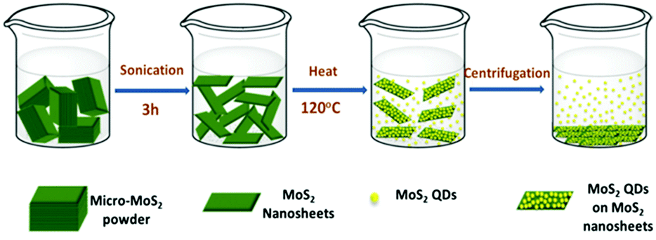
Uzcanga et al.109 carried out the preparation of MoS2 sonochemically using AHM and thiolacetic acid (CH3COSH) in water by completely dissolving them and the reaction mixture thus generated was treated with sonication for 1 h at a high ultrasound intensity (20 kHz) and the black precipitate was annealed at 400 °C in a H2/H2S atmosphere for 4 hours. During sonication, water decomposes to produce hydrogen radicals which then produce H2S gas on attacking thiolacetic acid acting as a sulfiding agent. Xu et al.110 synthesised MoS2 quantum dots (QDs) and nanosheets via a simple sonication method where MoS2 in DMF was sonicated to exfoliate MoS2. Following that, it was heated at 140 °C with stirring for several hours and then centrifuged to collect MoS2 QDs from the supernatant and QD and nanosheet mixture via centrifugation. The overall synthetic approach is depicted in Fig. 16.
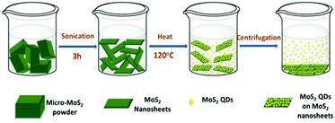 |
| | Fig. 16 Illustration of reaction steps for sonochemical synthesis of MoS2 QDs and nanosheets. Reprinted with permission from ref. 110 [S. Xu, D. Li and P. Wu, Adv. Funct. Mater., 2015, 25, 1127–1136]. Copyright WILEY-VCH Verlag GmbH & Co. KGaA, Weinheim. | |
Kristl et al.111 synthesised nanocrystalline MoSe2via a simple sono-chemical approach. The Mo(CO)6 and Se mixture in decalin was prepared in a sono-chemical reaction vessel. This slurry was then irradiated with high-intensity ultrasound for several hours under N2. The reaction temperature was maintained at 0 °C using a cooling bath. Amorphous MoSe2, thus formed, was then annealed at 330 °C for 12 h to obtain nanocrystalline MoSe2 spherical particles of 15–60 nm size analysed through TEM (Fig. 17(a)). The authors here commented on the very crucial role of temperature. The temperature of the reaction can reach up to 80 °C under these conditions and the rate of sono-chemical reactions decreases with an increase in temperature. When they kept the temperature of the water bath at 20 °C, there was an excess of Se in MoSe2 compared to the stoichiometric ratio. They found it to be because of unreacted Mo(CO)6 that sublimed and deposited on the walls before it could react with Se.
 |
| | Fig. 17 (a) TEM image of spherical MoSe2 NPs prepared sono-chemically. Reprinted with permission from ref. 111 [M. Kristl and M. Drofenik, Inorg. Chem. Commun., 2003, 6, 68–70]. Copyright Elsevier. (b) XRD pattern of MoSe2 nanodots and its comparison with bulk MoSe2. Reprinted with permission from ref. 113 [F. Qi and R. Liu, Nanoscale Res. Lett., 2019, 14, 67]. Copyright The Authors. (c) HRTEM image of MoTe2 indicating the interplanar distance. Reprinted with permission from ref. 114 [L. Qiu, V. G. Pol, Y. Wei and A. Gedanken, J. Mater. Chem., 2003, 13, 2985]. Copyright The Royal Society of Chemistry. | |
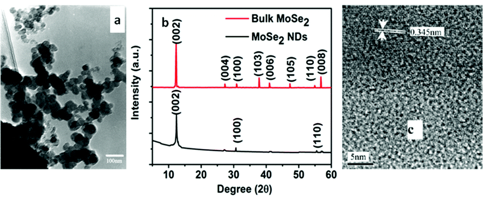
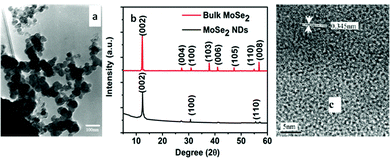
Yuwen et al.112 synthesized MoSe2 nanodots (NDs) from bulk MoSe2 by ultrasonication using the triblock copolymer F-127, which gets absorbed on the surface of MoSe2 particles and thereby offers water dispersibility. First, F-127 was dissolved in water to obtain a clear solution, followed by addition of MoSe2 and stirring for some time. This solution was then sonicated for 4 h in an ice bath with a 2 s on/off cycle at a high power. The authors adopted gradient centrifugation to separate MoSe2 NDs from larger particles. 2H-MoSe2 NDs of size in the range of 2–3 nm and thickness of up to three layers were obtained after 3–4 cycles of centrifugation. In another report, MoSe2 nanodots were retrieved from bulk-MoSe2via ultrasonication, conjugated with folic acid (FA) and stabilized by protein molecules. The corresponding XRD spectrum is shown in Fig. 17(b). Two peaks were observed at 700 and 800 nm in the absorbance spectra indicating a bandgap of 1.5–1.7 eV.113
In the synthesis of MoTe2, Mo(CO)6 was used as the precursor. The suspension of Mo(CO)6 and tellurium powder was sonicated for 4 h in an Ar atmosphere, followed by drying and calcination. First, they observed formation of a mixture of nanosheets and nanotubes which upon calcination transformed to nanotubes due to rolling of nanosheets. The nanotubes of 20–50 nm diameter and of length 100–500 nm were observed in the HRTEM images (Fig. 17c) with a d-spacing of 0.345 nm for the (004) plane of monoclinic MoTe2.114 The XRD also supported the formation of monoclinic MoTe2.
Mechanical exfoliation
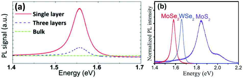
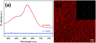
The process to peel off the atomically thin layer of a compound from its parent bulk crystals by micromechanical cleavage is called mechanical exfoliation. As MoX2 are layered materials held together by weak forces, atomically thin layers can easily be peeled using Scotch tape. These cleaved thin layers on the Scotch tape are normally placed on a substrate and can be transferred via rubbing carefully. The monolayer and multilayer nanosheets can thus be isolated once the Scotch tape is peeled off. Silicon oxide with a thickness of 200–300 μm is generally the substrate of choice.12,115–117 The method requires mild conditions, but the yield is very low. Additionally, there is little control over the number of layers being produced. In an attempt to resolve this, Dicamillo et al.118 used a rheometer as an automated tool for mechanical exfoliation and obtained few-layer flakes of MoS2 and MoTe2. This automation offers reproducibility and adds to the efficiency of this technique. Here, a Nitto Blue tape was used instead of the regular Scotch tape as the amount of residue left on the substrate was less. The only disadvantage of this procedure is a low yield; however, researchers prefer this method as it produces MoS2 layers of few micrometers thickness. Wafer anodic bonding was another modified method that promised a higher yield where one side of Pyrex glass was made anodic by placing pristine MoS2 and the other side was made cathodic. It was then subjected to a voltage of 200–1500 V at a temperature of 130–200 °C and an adhesive tape was used to mechanically peel off the flakes and transfer the thin film on the substrate.119 Tongay et al.120 exfoliated monolayer MoS2 and MoSe2 on a 90 nm SiO2 substrate and studied the effect of layer thickness and temperature on the PL intensity. In bulk, the bandgap of MoSe2 is 1.1 eV, and therefore weak PL emission is expected. Splendiani et al.117 also observed increased photoluminescence with a lower number of layers (emission peaks at 627 and 677 nm) which were absent in bulk MoS2. The increased PL emission in the single layer compared to multi-layer one was attributed to the indirect-to-direct bandgap crossover due to quantum confinement in the perpendicular direction. The PL intensity generally decreases for semiconductors with an increase in temperature as non-radiative processes are enhanced.120 Similar observations were observed for monolayer and few-layer MoS2 and few-layer MoSe2 but contradictory results were observed for single-layer MoSe2 (Fig. 18(a)).27 Several authors have reported the synthesis of MoSe2via mechanical exfoliation.26,121,122 Similarly, for preparation of nanocrystalline MoTe2, Ruppert et al.,32 Feng et al.123 and several other researchers also adopted the same method.124–133 In Fig. 18(b), the PL spectra of the MoS2 and MoSe2 monolayers synthesized by mechanical exfoliation are shown. Strong PL emission was observed at 1.56 eV and 1.85 eV for MoSe2 and MoS2, respectively.134 Yu et al.23 also reported the PL spectroscopy results of 1T′-MoS2 and 2H-MoS2 obtained by thermal annealing of 1T′-MoS2 (Fig. 19(a)). 1T′-MoS2 did not show PL emission; however, 2H-MoS2 has shown strong photoluminescence at about 670 nm which is probably due to interlayer interactions and spin–orbit coupling. Li et al.135 in their review article have discussed the relation of the PL bands to the number of layers. As the photoluminescence falls in the visible region, this property can be utilised for various applications such as photocatalysis, photonic devices, etc. The foremost shortcoming of this method is the production of small and arbitrary shaped flakes distributed over a surface, thus forbidding their use in large-scale applications.
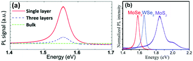 |
| | Fig. 18 PL spectra showing (a) thickness dependence in MoSe2. Reprinted with permission from ref. 27 [S. Tongay, J. Zhou, C. Ataca, K. Lo, T. S. Matthews, J. Li, J. C. Grossman and J. Wu, Nano Lett, 2012, 12, 5576–5580]. Copyright 2012 American Chemical Society. Comparison of (b) mono-layered MoS2 and MoSe2. Reprinted from ref. 134 [M. Yang, X. Cheng, Y. Li, Y. Ren, M. Liu and Z. Qi, Appl. Phys. Lett., 2017, 110, 093108] with the permission of AIP Publishing. | |
 |
| | Fig. 19 (a) PL spectra of 1T′ and 2H-MoS2.23 Reprinted with permission from Springer Nature [Y. Yu, G. H. Nam, Q. He, X. J. Wu, K. Zhang, Z. Yang, J. Chen, Q. Ma, M. Zhao, Z. Liu, F. R. Ran, X. Wang, H. Li, X. Huang, B. Li, Q. Xiong, Q. Zhang, Z. Liu, L. Gu, Y. Du, W. Huang and H. Zhang, Nat Chem, 2018, 10, 638–643] Copyright 2018, The Authors. (b) STEM image of 1T′-MoS2 (inset – Fourier transformed STEM image). Reprinted with permission from ref. 25 [C. Guo, J. Pan, H. Li, T. Lin, P. Liu, C. Song, D. Wang, G. Mu, X. Lai, H. Zhang, W. Zhou, M. Chen and F. Huang, J. Mater. Chem. C, 2017, 5, 10855–10860]. Copyright The Royal Society of Chemistry. | |
Chemical exfoliation
Chemical exfoliation overcomes the low-yield problem of mechanical exfoliation. It includes two approaches involving ion intercalation and solvent exfoliation. The ion intercalation method includes the insertion of small ions between the gaps of layers increasing the space between the layers. Then, these intercalated layers are reacted with water or some solvent like ethanol or methanol. Hydrogen gas is evolved during hydrolysis of ions and separates layers in single sheets suspended in the solvent. Mostly Li ions are used for intercalation due to their small size.136 The amount of lithium intercalated decides the phase purity of the material. Lin et al.137 used n-BuLi (n-butyl lithium) for exfoliation of layers from bulk MoS2. n-BuLi in hexane was added to MoS2 and sealed in an autoclave which was heated at 80 °C for 4 h. The dried LixMoS2 thus formed was hydrolyzed and sonicated for some time to obtain a colloidal suspension of MoS2 layers. In another report, ultrathin 1T′-MoS2 nanosheets were exfoliated from micro-MoS2 using Li2S. A mixture of MoS2, Li2S and Mo powders was taken in a quartz tube, sealed and heated to 800 °C for 10 h. The thus-obtained LiMoS2 powder was shaken in water for 12 h, which resulted in a colloidal solution of MoS2 nanosheets, and the 1T′ phase was confirmed by STEM (Fig. 19(b)).25 Although the low-yield problem of the mechanical exfoliation method gets resolved to some extent, the control over size and thickness gets reduced. Additionally, expensive reagents are required, and the problem of Li-ion toxicity exists. Impurities are easily introduced as the LixMoX2 compounds are highly air sensitive, thereby requiring extensive cleaning which hampers the yield and may even cause structural destruction.
Pulsed laser ablation
The pulsed laser ablation (PLA) method is extensively used for the preparation of NPs. In this process, a laser beam is used as the primary excitation source for the vaporisation of the metal precursor from the surface. A high energy pulsed laser beam hitting the target material generates high temperatures which vaporize the substance quickly. The wavelength and duration of the pulse (Hz), and laser ablation time are chosen depending upon the material to be synthesised. Han et al.138 synthesised MoS2 NPs via the PLA method where a MoS2 pellet was fixed at the bottom of a quartz tube in PVP solution and ablated for 10 min with continuous stirring using a Nd:YAG pulsed laser (10 Hz, 532 nm, and 100 mJ). The SEM images showed spherical nanoparticles (NPs), while TEM images revealed a layered structure. Likewise, Wu et al.139 synthesized MoSe2 IFs by ablation of the MoSe2 pellet in ethanol/water solution for 3 minutes using a Nd:YAG pulsed laser (10 Hz, 532 nm, and 300 mJ). Spherical NPs of 20 nm size were observed in SEM and TEM.
Analysis of phases and layer numbers
Raman spectroscopy
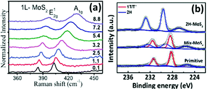
Raman spectroscopy is a reliable and non-destructive method to study lattice vibrations and phonon modes in materials. The Raman study becomes crucial when dealing with layered compounds. It is a very definitive tool to determine the number of layers in the synthesized samples. As MoX2 compounds exist in different phases, semiconducting as well as metallic, Raman spectroscopy is also the most convenient tool to identify these phases. Almost every report on synthesis of MoX2 compounds has mentioned the use of Raman spectroscopy for characterization. Kong et al.7 analysed the as-synthesized MoS2 using Raman spectroscopy where they observed two peaks for the E12g and A1g modes at approximately 380 cm−1 and 420 cm−1, respectively. Late et al.12 synthesized monolayer MoS2 whose Raman spectrum was then compared with that of bulk MoS2. Fig. 20(a) shows the out-of-plane A1g and in-plane E12g mode position in the Raman analysis of monolayer MoS2 and compares with the peak positions in the bulk form. Byrley et al.140 photochemically induced a 2H to 1T phase transition in MoS2 and monitored by Raman spectroscopy. The appearance of additional peaks at 330 and 370 cm−1 confirms the 1T phase and a distance of ∼20 cm−1 between E12g and A1g peaks indicated a MoS2 monolayer. Baledharan et al.80 reported that as the number of layers decreases, the intensity of the Raman peaks decreases. It has been reported that the distance between the out-of-plane A1g or B12g and in-plane E12g peaks is indicative of the number of layers and decreases when the thickness of the films increases.27 For example, a gap of almost ∼18 cm−1 indicates monolayer MoS2.86 Guo et al.25 very qualitatively represented the phase transformation in MoS2 through the Raman spectra of primitive (1T′-MoS2), mixed phase and 2H-MoS2 (Fig. 20(b)). Peaks at 156, 228, 283, 330, 403 cm−1 were obtained for 1T′-MoS2. The non-appearance of any peak at 383 cm−1 indicates the absence of the 2H counterpart.
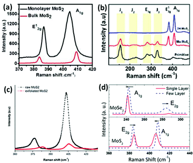 |
| | Fig. 20 (a) Raman spectra showing comparison between the phonon mode positions in bulk and monolayer MoS2. Reprinted with permission from ref. 12 [D. J. Late, B. Liu, H. S. Matte, V. P. Dravid and C. N. Rao, ACS Nano, 2012, 6, 5635–5641]. Copyright 2012 American Chemical Society. (b) Raman spectra of various phases. Reprinted with permission from ref. 25 [C. Guo, J. Pan, H. Li, T. Lin, P. Liu, C. Song, D. Wang, G. Mu, X. Lai, H. Zhang, W. Zhou, M. Chen and F. Huang, J. Mater. Chem. C, 2017, 5, 10855–10860]. Copyright The Royal Society of Chemistry. (c) Blue shift in Raman peaks observed for exfoliated MoS2. Reprinted with permission from ref. 144 [D. Van Thanh, C.-C. Pan, C.-W. Chu and K.-H. Wei, RSC Adv., 2014, 4, 15586–15589]. Copyright The Royal Society of Chemistry. (d) Thickness dependence of the Raman spectra of MoS2 and MoSe227 [S. Tongay, J. Zhou, C. Ataca, K. Lo, T. S. Matthews, J. Li, J. C. Grossman and J. Wu, Nano Lett., 2012, 12, 5576–5580]. Copyright 2012 American Chemical Society. | |
The doublet in the range of 380–420 cm−1 is characteristic of 2H-MoS2.141 Although most of the reports support that blue and red shifts are observed in the A1g and E12g peaks, resulting in a decreased peak distance,142 there are a few studies which report divergent behaviour. For instance, Zhu et al.143 observed Raman frequencies at 379.6 and 401.8 cm−1 for 4 nm thickness, blue-shifted from the pristine MoS2. The reason provided by them was the distortion in the structure due to intercalating ion induced strain. Thanh et al.144 reported a blue shift in the Raman peaks (Fig. 20(c)) when MoS2 layers of 1.5 to 3.5 nm thickness were produced via N2 quenched exfoliation. The peak distance however decreased, consistent with other reports. Yang et al.145 observed blue and red shifts in both the Raman peaks upon inducing strain in the plane and out of the plane, respectively.
2H-MoSe2 shows 12 modes of vibration, of which A1g, E1g, E12g, and E12g are Raman active. As shown in Fig. 20(d), the out-of-plane A1g is the more prominent peak at about 240 cm−1 and the peak at 280 cm−1 is reported to be due to the E12g in-plane mode of vibration.27 A peak at around 350 cm−1 due to the interlayer interaction is also considered as a characteristic peak which is absent in monolayer MoSe2.134
Likewise, Raman spectroscopy is also often used to identify various phases of MoTe2 where the 2H-phase exhibit peaks at 119, 171, 233 and 289 cm−1 corresponding to in-plane E1g, out-of-plane A1g, in-plane E12g and out-of-plane B12g modes, of which
the peak at 233 cm−1 was the most prominent.99,106 In another report, the peaks at 171.4 (A1g), 234.7 (E12g), and 290.0 cm−1 (B12g) corresponded to the major Raman vibrational modes of 2H-MoTe2.29 It is also reported that the thickness of the MoTe2 layers can be determined by the intensity ratio of the B12g and E12g peaks, e.g. a decrease in the ratio means an increase in the number of layers. In the case of the 1T′-phase of MoTe2, it has been reported that the chalcogenide layer is slightly offset compared to other phases, resulting in a distorted structure which gives rise to a higher number of Raman peaks compared to the 2H-phase. Empante et al.106 observed Raman peaks at 80, 85, 102, 112, 126 and 162 cm−1 for the 1T′-phase and some additional peaks at 189 and 257 cm−1 were also reported by Zhou et al.99 Generally, the broad peaks at 155 and 242 cm−1 can be related to the 1T-phase of MoTe2.106
Few-layer MoTe2 shows also a characteristic out-of-plane B12g peak which is normally absent in monolayer and bulk MoTe2. Also, the peak at about 255 cm−1 for multilayer MoTe2 can be tuned and a blue shift for the monolayer may be realized.160Table 3 summarises the Raman peak values of MoX2 from various reports. However, these values may vary from report to report as the peak positions are phase and thickness dependent. Fig. 20(d) shows a representation of the effect of layer thickness on the Raman peaks of MoS2 and MoSe2.27 It is also well known that the Raman peak values are dependent upon the wavelength of laser light used.122 Yang et al.134 studied the variations in the Raman frequencies of MoS2 and MoSe2 with temperature and pressure. Fig. 21(a) shows that the peaks are blue-shifted on increasing pressure. However, a red shift was observed by the authors when the temperature was increased. Inter-atomic interactions are enhanced when the pressure is increased causing compression of the out-of-plane mode leading to broadening of the A1g peak in comparison to the E12g peak. Similarly, with an increase in temperature, the kinetic energy increases. Therefore, inter-atomic interactions are diminished, and a red shift was observed.
Table 2 Comparison of the synthesis methods, properties and performance of molybdenum dichalcogenides in various applications
| Method |
Nanomaterial |
Morphology and properties |
Application |
Performance |
Ref. |
| Hydrothermal |
2H-MoS2, 2H-MoSe2 |
Average size ∼ 4 nm, average size ∼ 7 nm, |
— |
— |
146
|
|
|
2H-MoS2 |
λ
abs ∼ 450, 618 and 665 nm, bi-layer with a lateral size of ∼200 nm−1 μm |
p-Si/n-MoS2 photodetectors Photocatalysis |
Rectification ratio of 1000 order Rhodamine B degradation |
147
|
|
|
MoS2 QDs |
Size ∼ 8 nm |
Atrazine aptasensors based on MoS2 QDs/TiO2 nanotubes |
Detection limit up to 1 pM |
148
|
|
|
MoS2 |
Nanoflowers with a size of about 300 nm composed of nanosheets |
Supercapacitors |
Specific capacitance – 122 F g−1 at 1 A g−1 |
149
|
|
|
2H-MoS2 |
Nanoflowers |
Supercapacitors |
Specific capacitance – 106 F g−1 |
150
|
|
|
2H/1T-MoSe2 |
Nanoflowers composed of nanosheets: specific surface area – 38.14 m2 g−1 and specific pore volume – 0.17 cm3 g−1 |
Full spectrum absorption |
— |
151
|
|
|
2H/1T-MoSe2 |
Few-layer nanosheets: λabs ∼ 440, 500, 705 and 800 nm, surface area – 23 m2 g−1 |
HER |
Tafel slope ∼ 75 mV dec−1 |
56
|
| Solvothermal |
2H-MoSe2 by use of olive oil as a surfactant |
Mono-bilayer with 500 nm lateral dimensions, λabs ∼ 672 and 791 nm, λem ∼ 376.6 nm; Eg = 0.83 eV |
Photodetectors |
Response time ∼ 8 s, external quantum efficiency ∼ 50% |
152
|
| Thermal |
2H-MoSe2 |
Nanoflowers ∼ 400 nm |
HER |
Overpotential ∼ 230 mV, Tafel slope ∼ 82 mV dec−1 |
153
|
| Microwave |
MoSe2 |
Spherical nanoparticles and nanorods: crystallite size – 11–16 nm |
— |
— |
154
|
|
|
2H-MoSe2 |
Mesoporous dry-leaf like morphology: specific surface area – 64.63 m2 g−1 |
HER and supercapacitors |
Tafel slope ∼ 82 mV dec−1, specific capacitance – 257.38 F g−1 at 1 A g−1 |
155
|
| CVD |
MoS2 |
Triangular monolayers with a lateral size of 10–50 μm |
Photodetectors |
Photoresponsivity – 2.5 × 10⁴ A W−1, specific detectivity – 4.1 × 10¹⁴ Jones |
156
|
|
|
MoSe2 |
|
Photodetectors |
Photoresponsivity – 859 mA W−1, specific detectivity – 1.55 × 10¹¹ Jones, response time ∼38 ms |
157
|
| Liquid exfoliation |
MoS2 |
Thickness <10 layers with lateral dimensions of up to 90 nm, λabs ∼ 610, 669 nm |
HER |
Overpotential ∼ 420 mV, Tafel slope ∼ 41 mV dec−1 |
158
|
| Mechanical exfoliation |
MoSe2 |
λ
em ∼ 780 nm, average decay time ∼ 1.08 ns |
Photodetectors |
— |
159
|
Table 3 Typical Raman values for MoX2 (X = S, Se, Te)
| Material |
Raman active modes |
Raman frequency (cm−1) |
Ref. |
| MoS2 |
E12g |
385.8 |
86
|
|
|
A1g |
403.8 |
|
| 2H-MoS2 (monolayer) |
E12g |
382.3 |
134
|
|
|
A1g |
402.1 |
|
| 2H-MoS2 (multilayer) |
E12g |
381 |
80
|
|
|
A1g |
406 |
|
| 2H-MoS2(mono/bilayer) |
E12g |
380 |
161
|
|
|
A1g |
404 |
|
| 2H-MoSe2 |
E12g |
283.8 |
52
|
|
|
A1g |
239.9 |
|
| 2H-MoSe2 |
E12g |
284.9 |
5
|
|
|
A1g |
239.7 |
|
| 2H-MoTe2 |
A1g |
171.4 |
29,162
|
|
|
E12g |
234.7 |
|
|
|
B12g |
290.0 |
|
| 1T′-MoTe2 |
Bg |
163 |
29,162
|
|
|
Ag |
262 |
|
| 1T′-MoTe2 (monolayer) |
Ag |
112 |
160,163
|
|
|
|
127 |
|
|
|
|
161 |
|
|
|
|
252 |
|
|
|
|
269 |
|
| 2H-MoTe2 (few-layer) |
E1g |
119 |
99
|
|
|
A1g |
171 |
|
|
|
E12g |
234 |
|
|
|
B12g |
289 |
|
| 1T′-MoTe2 |
Au |
107 |
99,164
|
|
|
Ag |
126.9 |
|
|
|
Bg |
163 |
|
|
|
Ag |
256.1 |
|
 |
| | Fig. 21 (a) Raman spectra of MoS2 pressure dependence on Raman modes. Reprinted from ref. 134 [M. Yang, X. Cheng, Y. Li, Y. Ren, M. Liu and Z. Qi, Appl. Phys. Lett., 2017, 110, 093108] with the permission of AIP Publishing. (b) XPS spectra of 2H-MoS2, the 2H/1T′ mixture and 1T′-MoS2 (primitive). Reprinted with permission from ref. 25 [C. Guo, J. Pan, H. Li, T. Lin, P. Liu, C. Song, D. Wang, G. Mu, X. Lai, H. Zhang, W. Zhou, M. Chen and F. Huang, J. Mater. Chem. C, 2017, 5, 10855–10860]. Copyright The Royal Society of Chemistry. | |
X-Ray photoelectron spectroscopy (XPS)
XPS is another important tool to obtain useful information about the bonding, structure/phases and morphology of these compounds. The CVD method generally involves the use of MoO3 as the Mo precursor, and the extent of reaction completion can be estimated from the XPS spectra. Molybdenum is present as Mo+6 in MoO3 and shows binding energies of 232.5 and 235.9 eV for 3d5/2 and 3d3/2, respectively, while these values are much lower in respective chalcogenides.5 The typical binding energies of various elements in MoX2, e.g. Mo, S, Se and Te, are listed in Table 4. Fig. 21(b) shows the binding energy position and shift in peaks on transforming the phase. The binding energies are slightly higher for the 2H-phase than for 1T′-MoS2. The peaks for Mo+4 for MoS2 in the 2H phase appear at around 230 and 233 eV which shift to a lower energy transformation of the semiconducting phase to the metallic phase.25 Byrley et al.140 observed similar phenomena where the broadening in the peaks indicated a mixture of both the phases with peaks at 230 and 233 eV shifted to lower energies. Wang et al.165 reported a peak shift in Mo(3d5/2) and S(2p) in MoS2 nanoparticles by +1.6 eV and −2.2 eV, respectively, in comparison to elemental Mo and S because of partial electron transfer from the Mo metal to the chalcogen owing to the greater electronegativity of S than Mo. As a result, Mo gains a partial positive charge which is reflected by the increase in binding energy and sulfur gains a negative charge, hence a decrease in binding energy.43
Table 4 Typical binding energies of the corresponding elements in MoX2 compounds
| Material |
Peaks (binding energy) |
Ref. |
| Mo3d5/2 |
Mo3d3/2 |
Te3d5/2 |
|
Te3d3/2 |
| 2H-MoTe2 |
228.2 |
231.4 |
572.9 |
|
583.3 |
29
|
| 2H-MoTe2 |
228.3 |
— |
572.9 |
|
— |
162
|
| 1T-MoTe2 |
227.7 |
231.0 |
572.1 |
|
582.5 |
160
|
|
|
|
|
Mo3d5/2 |
Mo3d3/2 |
Se3d5/2 |
|
Se3d3/2 |
|
| 2H-MoSe2 |
229 |
232 |
54.4 |
|
55.3 |
52
|
| 2H-MoSe2 |
229.5 |
232.9 |
55.5 |
|
56.4 |
166
|
| 2H-MoSe2 |
229.7 |
232.8 |
54.7 |
|
55.4 |
5
|
| 2H-MoSe2 |
229.0 |
232.1 |
— |
|
— |
23
|
| 1T′-MoSe2 |
228.1 |
231.2 |
— |
|
— |
23
|
|
|
|
|
Mo3d5/2 |
Mo3d3/2 |
S2p3/2 |
S2p1/2 |
S2s |
|
| 2H-MoS2 |
229.1 |
232.1 |
161.25 |
162.94 |
226.25 |
43
|
| 2H-MoS2 |
229.1 |
232.2 |
— |
— |
226.1 |
23
|
| 2H-MoS2 |
229.6 |
232.7 |
162.4 |
163.6 |
— |
81
|
| 1T′-MoS2 |
228.2 |
231.3 |
— |
— |
|
25
|
| 1T′-MoS2 |
228.3 |
231.4 |
— |
— |
225.3 |
23
|
| MoS2 |
229.3 |
232.4 |
— |
— |
— |
66
|
X-Ray diffraction (XRD) technique
XRD patterns give a clear indication of the phase of MoX2 compounds with measurement of the cluster size and also provides information on lattice spacings. The XRD peak positions for 2H-MoS2 are reported to be around 2θ ∼14°, 32.7°, 33.5°, and 58.3° prominently due to the [002], [100], [101] and [110] planes, respectively.46,60,80,86 The peak at 2θ = 14° is the most intense one in MoS2 and can give information about the phase and the number of layers as it varies marginally even with slight changes in the structure and morphology. It is reported that the absence of a peak at 2θ = 14.4° is a typical characteristic of monolayer MoS2.43 Similarly, the peak at about 14.8°, typical for 1T′-MoS2, may shift to lower angles (∼14.4°) when transformed to the 2H phase (Fig. 22(a)).23 Other Mo-chalcogenides show similar behaviour, e.g. an almost 0.3° variation has been shown in the case of 1T′ and 2H-MoSe2 for the peak at ∼13.9° (Fig. 22(b)).23
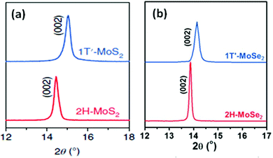 |
| | Fig. 22 Variation in XRD peaks depending upon the phase of the (a) MoS2 and (b) MoSe2 compounds. Reprinted with permission from ref. 23 [Y. Yu, G. H. Nam, Q. He, X. J. Wu, K. Zhang, Z. Yang, J. Chen, Q. Ma, M. Zhao, Z. Liu, F. R. Ran, X. Wang, H. Li, X. Huang, B. Li, Q. Xiong, Q. Zhang, Z. Liu, L. Gu, Y. Du, W. Huang and H. Zhang, Nat. Chem., 2018, 10, 638–643.]. Copyright 2018, The Author(s). | |
Atomic force microscopy (AFM)
AFM is a conclusive tool to estimate the number of layers/thickness of the deposited materials. Dividing the height of the as-synthesized layers by the thickness of one layer gives a good estimation of the number of layers present in the as-synthesized material.110,161 Zhou et al.99 found the height of the as-prepared MoTe2 through AFM to be approximately 3.1 nm. The interlayer spacing of MoTe2 is about 0.7 nm, and therefore a four-layer MoTe2 film was formed. Fig. 23 shows the AFM image of the MoS2 flakes obtained from CVD and mechanical exfoliation methods.80,117 The interlayer spacings for MoS2, MoSe2, and MoTe2 are 0.615, 0.646 nm167 and 0.691 nm,76 respectively. Therefore, the film thickness divided by interlayer spacing gives the number of layers of MoS2. The figures display multilayer formation at different positions in the sample. Similarly, Tongay et al.120 analysed monolayers of MoS2 and MoSe2 through AFM images.
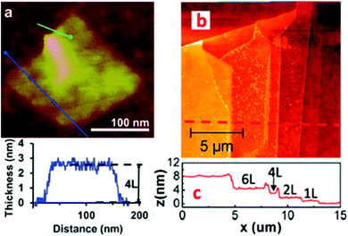 |
| | Fig. 23 AFM image of (a) CVD grown (reprinted with permission from ref. 80 [S. Balendhran, J. Z. Ou, M. Bhaskaran, S. Sriram, S. Ippolito, Z. Vasic, E. Kats, S. Bhargava, S. Zhuiykov and K. Kalantar-Zadeh, Nanoscale, 2012, 4, 461–466], Copyright The Royal Society of Chemistry) and (b) mechanically exfoliated MoS2 flakes with the height profile along the red line. Reprinted with permission from ref. 117 [A. Splendiani, L. Sun, Y. Zhang, T. Li, J. Kim, C. Y. Chim, G. Galli and F. Wang, Nano Lett., 2010, 10, 1271–1275]. Copyright 2010 American Chemical Society. | |
Applications
Mo–chalcogenide nanostructured materials offer great scope in modern technological advancement. They are suitable for a variety of electronic and optoelectronic applications due to tailoring of their band gap and nature of the structure, e.g. simple spherical nanoparticles to layered structures can alter the properties, leading to possibilities of new applications. Not only pure MoX2 nanostructured materials but their hybrid counterparts add tremendous value in converting traditional applications to modern requirements. In search of hybrid materials, researchers tried to combine nanoparticles with graphene for betterment of electrical and thermal properties. Indeed, it has been reported that graphene, having excellent conductivity when combined with MoX2, may get further enriched, opening new avenues in the field of catalysis. In addition, MoX2 can tackle the no bandgap problem of graphene. Therefore, the fabrication of hybrid structures achieving a synergistic effect is the latest research trend. Several reports and reviews were published discussing various applications of Mo–chalcogenides and a few of them are referred in this article.168,169
Mo–dichalcogenides have been proposed as potential materials for energy applications such as thermoelectrics,170 Li/Na-ion batteries,10 supercapacitors,11etc. Due to the high ionic conductivity and surface area, they are potential materials for electrical double layers in supercapacitors.171 Hydrothermally synthesized MoSe2 has shown a specific capacitance of 133 F g−1 at a current density of 2 A g−1 in a full solid-state supercapacitor, thereby opening avenues for flexible supercapacitors.172
Table 2 presents some of the important applications of MoX2 compounds prepared by various methods. The following sections discuss some selected applications of layered molybdenum dichalcogenide compounds in their intrinsic forms and integrated with other materials wherever seems appropriate.
Catalysis
Electrocatalysis.
The world is pursuing renewable and clean sources of energy. Molecular hydrogen is by far the cleanest fuel. Given the right catalyst, the hydrogen evolution reaction (HER) is the most efficient and simplest electrode reaction to produce hydrogen. Production of hydrogen via splitting of water through the HER is a 2e− electrochemical reaction and is believed to be an excellent way to produce renewable hydrogen fuel. In the HER, the H+ ions from the solution combine with electrons on the surface of the catalyst to produce H2 gas. Therefore, adsorption and binding of hydrogen becomes the most essential step. This step is quantized in the form of Gibbs free energy of adsorption (ΔGH). The lower the ΔGH value, the higher the binding efficiency. The layered nature of MoX2 compounds makes them highly suitable for catalysis due to the presence of dangling bonds and exposed edges,7,173 whereas basal planes are catalytically inert. Therefore, nanosized MoX2 are more active due to increased accessible edges as compared to their bulk counterparts due to the increased surface area.
HER devices use acidic electrolytes, and hence MoS2 and MoSe2 act as acid-resistant catalysts.174 Several reports have reported the remarkable capability of MoX2 compounds in the HER. In HER electrocatalysis, the HER catalyst should minimize the overpotential and should have a low Tafel slope (intrinsic properties of the catalyst) and consequently increase the process efficiency. It is therefore warranted that researchers should undertake advanced research to develop highly active HER catalysts including materials that are highly abundant and inexpensive. The HER on a commercial Pt surface gives a Tafel slope of ∼ 30 mV dec−1, while commercial MoS2 shows a value of ∼115 mV dec−1. MoS2 has the advantages of being resistant to sulphur poisoning and highly reactive. Xu et al.110 explored MoS2 QDs and nanosheets for HER performance. The QDs gave an overpotential of about 350 mV, whereas the mixture gave an overpotential of 120 mV which was due to the high number of active edges in interspersed QDs and nanosheets and obtained a Tafel slope of ∼69 mV dec−1. There was a negligible change in performance even after the 2000th cycle. The main focus is to maximize exposed sites to obtain a higher efficiency. For this motive, MoS2 has been supported on various materials like Au, graphene, CdS, ZnS, carbon fibres, SiO2, etc. MoS2/RGO hybrids synthesized by Yanguang Li and co-workers60 gave a very low overpotential and a small Tafel slope. They obtained a Tafel slope of ∼41 mV dec−1 from MoS2/RGO hybrids. This catalyst was reported to be highly durable and reproducible even after 1000 cycles. The progress in MoS2 based HER performance was thoroughly reviewed by He et al.175
On the other hand, MoSe2 show HER performance with a much lower Tafel slope and a lower overpotential than MoS2 as MoSe2 provides a higher coverage area for hydrogen adsorption.52 Guo et al.176 fabricated a nanocomposite of MoSe2/RGO and found that the electrocatalytic activity was well comparable to that of the commercial Pt/C material. The role of electrical conductivity is very pivotal for HER performance. The electrical conductivity of 1T-MoX2 is much higher than that of 2H-MoX2. Using 1T-MoX2 provides more active sites and a greater electrical conductivity leading to an enhancement in HER activity.177–179 Zhang et al.180 reported core–shell type 1T@2H-MoSe2 nanosheets via a simple hydrothermal method with excellent HER performance having a Tafel slope of 41 mV dec−1 equal to that reported for MoS2 and an overpotential of 20 mV.60 Huang et al.181 synthesized MoSe2/SnO2 composites where MoSe2 nanosheets were decorated on SnO2 nanotubes. This open structure made the edges fully accessible leading to high HER activity with a Tafel slope of 51 mV dec−1. These reports suggest that a secondary material is required in order to expose the edges and make full utilisation of these MoX2 compounds. Similarly, Singh et al.182 reported the improved performance of the MoSe2/SnS nanocomposite for water splitting.
When it comes to tellurium-based Mo nanostructures, 2H-MoTe2 was found to be catalytically inert; however, 1T-MoTe2 was found to be a competent electrocatalyst for the HER with a moderate current density of −10 mA cm−2 at about 360 mV in sulfuric acid.183,184 Likewise, Qiao et al.185 reported liquid exfoliated MoTe2 nanosheets for electrocatalytic activity showing a Tafel slope of 118.9 mV dec−1 with an overpotential of 309 mV. As the HER activity is extensively dependent on the exposed edges, a large portion of the layered surface, i.e., the basal plane, remains useless. By activating the basal planes of 1T′-MoTe2, McGlynn et al.28 reported an improvement of overpotential in MoTe2 from 320 to 178 mV with the Tafel slope increasing to 116 mV dec−1 from 68 mV dec−1. This value was obtained by applying a reverse bias to the MoTe2 electrodes which introduced extra electrons leading to activation of basal planes resulting in superior HER activity. There is truly little research carried out for HER applications of MoTe2 and it may be possible to further enhance its applicability by combining it with other materials. In view of this, Donglin Lu and co-workers186 synthesized 1T′-MoTe2 on a carbon cloth substrate via the CVD process. The activity of the material was evident from the Tafel slope value of 127 mV dec−1 and the overpotential value of −230.7 mV. The inter-combination of MoX2 may further enhance their activity, but no reports on that matter can be found. Hence, this area can be looked upon to expand their application and gain more insights into their properties.
Photocatalysis.
MoS2, being chemically inert, easily available, and having low toxicity, good thermal stability and high absorption capacity, has been considered as a useful heterogenous photocatalyst for dye degradation and water decontamination through advanced oxidation processes (Fig. 24). The small bandgap of TMDs, especially those of MoS2 and MoSe2, allows solar energy to be harvested in the visible region for photocatalytic degradation of organic pollutants. The narrow bandgap of nano-MoSe2 (∼1.55 eV) is highly resistant to photocorrosion. The photocatalytic activity of MoSe2 is limited by virtue of a higher charge carrier recombination rate, poor visible light adsorption and a low electrical conductivity. These drawbacks can be overcome by the synergistic effect of other nanomaterials. Many reports mention the use of TMD composites with other materials like ZnO, TiO2, GO, and rGO as photocatalysts.187 The review article by Wu et al.188 gives a general comparison of the photocatalytic efficiency of MoS2 in combination with such materials. Ritika et al.18 observed more than 95% degradation of 10 ppm methylene blue (MB) solution in 20 minutes using a meager quantity (0.15 g l−1) of the MoS2–ZnO catalyst. However, the degradation percentage was found to be pH dependent with maximum degradation observed at pH 11. According to them, the combination of MoS2 and ZnO has reduced the recombination rate of charge carriers due to fast charge transfer in the conduction bands of MoS2 and ZnO leading to a high rate of reaction. Wu et al.189 synthesized MoSe2 composites with reduced graphene oxide (rGO) so as to minimize the recombination rate and increase the charge transfer. The hydrothermal method resulted in formation of 2–3 layer thick MoSe2 nanosheets vertically aligned on the surface of rGO. These nanocomposites were able to remove more than 90% of MB and RhB effluents. Haipengchu et al.50 reported up to 90% reduction of Cr(VI) in visible light in 2 h with MoSe2/TiO2 nanocomposites. They also compared the results with those of individual MoSe2 and TiO2 which resulted in a much lower reduction of the same up to 60% and 5% only. The maximum efficiency was obtained when the ratio of MoSe2 and TiO2 was 2:1 and further increase in the amount of TiO2 decreased the reduction efficiency. Mittal et al.190 studied the photocatalytic activity of MoSe2 and polyaniline (PANI) nanocomposites. These composites were effective against both cationic and anionic dyes due to the presence of both +ve and −ve charges on the surface and thus 80% degradation was observed for Congo red (CR) and Rhodamine B (RhB) by a MoSe2/PANI composite with a 2:1 ratio.
 |
| | Fig. 24 Typical photodegradation mechanism via advanced oxidation processes (AOPs). | |
Huang et al.191 were even successful in degrading nitro aromatic compound contaminants present in water with the help of the as-synthesized MoSe2 microspheres composed of MoSe2 nanosheets. However, in the case of Mo-tellurides, out of two phases of MoTe2, only the 2H phase has fairly good photoresponsivity to visible and infrared light.192
Water desalination and decontamination
Shortage of clean potable water is the major problem faced by most of the population. It is realized by the researchers that, without disturbing natural hydrological cycles, seawater desalination technologies are the best alternative to the problem of water shortage. Driven by their huge ecological benefits, they are gaining a lot of research interest. MoS2 nanosheets are highly effective in decontaminating water by absorbing heavy ions. The monolayer nanosheets have a high absorption capacity due to a high surface area and excellent affinity towards many transition metal ions (heavy metals) such as Hg2+, Ag+, Pb2+, Zn2+, and Cd2+ (soft Lewis acids) due to the presence of S2− ions (soft Lewis base) on the exposed edges. The order of selectivity is Hg2+> Pb2+> Zn2+> Cd2+ according to the order of their softness. These negatively charged ions are also helpful in dispersing these nanomaterials into water. The H+ or other intercalating ions such as Li+ are present in contaminated water as counterions with a negative charge on the surface. These ions are replaced by the contaminant metal ions and make complexes with sulfur ions, leading to decontamination of water. Another factor in the adsorption of these ions on the nanosheets is that the ions in the water are pulled and hold together by the surface ions through electrostatic force of attraction. Thus, the whole process is believed to be based on the interaction at the surface as well as the inner layer complex formation.193 Therefore, the best adsorbent for decontamination would be the one with a higher sulphur content, large surface area and high pore volume having enough size to accommodate the ions. Kankeu et al.194 recently synthesized MWCNT/MoS2 hybrids loaded with mercaptopropyl trimethoxysilane to create a sulfur rich surface and then tested them for removing mercury ions from water. A high absorption capacity of 0.9661 mg g−1 was achieved, and the study also revealed that the decontamination takes place through the chemisorption phenomenon. Ai et al.195 reported the absorption capacity of the hydrothermally prepared MoS2 nanosheets as high as 2563 mg g−1 and excellent mercury selectivity. The concentration of mercury ions was drastically reduced from 10000 ppb to 0.3 ppb by using 10 mg of the adsorbent for 100 mL solution. MoS2 adsorbents are also highly efficient in absorbing cationic/alkaline dyes like MB, malachite green (MG), and RhB196 through van der Waals forces and electrostatic forces of attraction. Massey et al.197 in their study found that 0.1 g of the synthesized MoS2 nanosheets were able to adsorb 90% of MB within 10 minutes from its >100 ppm solution and has shown good recyclability. Similarly, an 80% removal efficiency was observed in the case of MG and RhB within an hour. However, acidic dyes like CR and fuchsin acid have shown very low adsorption. In contrast to most studies, fungus like MoS2 nanosheets, hydrothermally prepared by Song et al.,198 were selective towards Congo red instead of MB or RhB. MoS2 nanosheets with a contact angle greater than 80° (against water) exhibit hydrophobicity and hence can be helpful in removal of oils from water.199 These nanostructures having high adsorption properties combined with photocatalytic properties serve as productive and cost-efficient materials for water purification. A review article discussing specifically the adsorption of heavy metal ions in water on MoS2 has been recently published. It thoroughly explains the mechanism involved, the factors affecting the adsorption process and its efficiency compared to other adsorbents.200 In their study, Hieranian et al.201 applied membrane technology for the desalination of water. As it is obvious that the thinner the membrane, the greater the water flux through it, single layer MoS2 nanosheets with nanopores were applied, achieving a desalination capacity up to 80%.
Sensors
The use of nanocrystalline MoX2 as a sensing material is widely being studied. The most reported MoX2 based sensors are field effect transistor (FET) type. The advantage of MoS2 in FETs has been thoroughly reviewed by Singh et al.202 The general device structure of a FET with the example of MoS2 as the sensing material is depicted in Fig. 25.203 The strength of MoX2 transistors lies in a large bandgap, which offers a high on/off ratio, and the layered nature provides excellent electrostatic integrity. Therefore, they can overcome the limitations in graphene-based devices due to the absence of bandgap despite having an excellent mobility of up to 2 × 105 cm2 V−1 s−1.204 They may not be ideal candidates for high performance applications but they can be conveniently utilized for applications having low-power requirements. MoS2-based FET sensors have exhibited exceptional charge carrier mobilities and high on/off ratios with great sensitivity in the detection of biomolecules, heavy metal ions, and toxic gases.193 The following sub-sections discuss the use of molybdenum dichalcogenides in gas sensors, photo-detectors and bio-sensors.
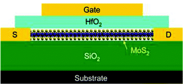 |
| | Fig. 25 Representation of the device structure of a MoS2 transistor. Reprinted with permission from ref. 203 [Y. Yoon, K. Ganapathi and S. Salahuddin, Nano Lett., 2011, 11, 3768–3773]. Copyright 2011 American Chemical Society. | |
Gas sensors
Gaseous toxicity detection is an essential requirement for human and environmental health. The timely monitoring and understanding of effluents from industries and the environment is a burning issue for living organisms. In this regard, the development of 2D sensors which can work at room temperature has become important. Several reports endorsed nano-MoS2 for gas-sensing applications due to the ample surface area and abundant surface-active sites. Yoon et al.203 reported a 0.5 to 320 cm2 V−1 s−1 variation in field effect mobility values with an on/off >1010 order of magnitude when sensing was performed using a thin MoS2 FET. MoS2-based FET devices are useful in the detection of various gases (e.g., H2, NH3, and NO2).13,205 As the 2D configuration allows better adsorption of gas molecules, most reports use MoS2 nanosheets for gas detection.206 Li et al.207 detected NO gas up to the conc. of 0.8 ppm through a mechanically exfoliated MoS2 nanosheet based FET and also observed that multilayer MoS2 was more efficient than the monolayer analogue. It is reported that the resistance increases due to the absorption of electron-withdrawing NO on MoS2.208 Late et al.26 reported a room temperature MoSe2 sensor for the detection of NH3 up to a level of 50 ppm. The detection of hazardous NO2 and NH3 gases up to a level of 1 ppm was reported using a MoSe2 based FET sensor209 and up to a level of 20 ppb for exfoliated MoS2.210 It is often realized that MoX2 nanomaterials offer high sensitivity, but the recovery time is longer when compared to metal oxides.211,212
Photo-detectors
Atomically thin MoS2 shows excellent sensing towards chemicals and gaseous molecules and is also a very good photosensor owing to its sensitivity to the external environment and illumination conditions. Late et al.12 synthesized monolayer MoS2 FETs and studied the origin of hysteresis in these devices. They stated that the main cause of hysteresis was the absorption of water molecules which induce trap states in the material. The authors also mentioned that with MoS2 being highly photosensitive, white light illumination can significantly contribute to hysteresis. It was thereby suggested that the controlled hysterical behaviour of FETs can be utilized in humidity sensors and the photosensitive behaviour can be utilised in photo-detectors.213 Li et al.116 fabricated phototransistors using 1L MoS2 and SiO2 as dielectric layers which have shown a photo-responsivity of 7.5 mA W−1 at an applied voltage of nearly 50 V. Similarly, phototransistors fabricated from 1L to 3L MoS2 exhibited a photo-responsivity of nearly 100 mA W−1 at an applied voltage of up to 10 V. The report has also shown that 1L and 2L MoS2 detected green light and 3L nanosheets were responsive to red light.214 Lopez-Sanchez et al.215 fabricated 1L-MoS2 phototransistors and reported an excellent photoresponsivity of 880 A W−1. Hang et al.121 fabricated phototransistors based on 3L MoSe2, demonstrating an on/off ratio of ∼105 and a carrier mobility of 1.79 cm2 V−1 s−1. The humidity sensors developed from MoSe2 nanoflowers showed a sensitivity of more than 70% with response and recovery times of 53 seconds and 13 seconds, respectively.14 Selamneni et al.216 fabricated a near infrared (NIR) photodetector incorporating MoSe2 nanoflowers onto cellulose paper and reported a photoresponsivity of 9.73 mA W−1 when illuminated by 780 nm light and the expected improvement with an enhancement in light intensity. The fabricated device was flexible and robust in nature, promising its future in nanoelectronics. Having a narrower bandgap than nano-MoS2 and MoSe2, nano-MoTe2 is a favourable candidate for NIR photodetectors. The use of thin layered MoTe2 is very prominent in FETs.129,217 Few-layer MoTe2 has the least direct bandgap in the MoX2 family and therefore can be operated in the visible to infrared energy range. Giri et al.218 reported 3L MoTe2 photodetectors showing photoresponsivities over the range of 300 to 1100 nm with a maximum photoresponsivity of ∼53.1 mA W−1 at 870 nm and a minimum value of 30 mA W−1 at 1100 nm. By introducing an electron tunnelling mechanism, interestingly, Yin et al.124 reported an outstanding photoresponsivity of 2560 A W−1 and an electron mobility of 25.2 cm2 V−1 s−1 using few-layered MoTe2 as the channel in a transistor.
Bio-sensors
Owing to their excellent electrochemical and luminescence properties, MoS2-based nanomaterials have been endorsed as excellent biosensing probes for the analyte detection over a wide range.219 Due to their luminescence quenching properties and multidimensional structures, such chalcogenides can cover a wide band of applications.193 Indeed, there are several reports that document successful utilization of MoS2 nanosheets in the detection of biomolecules and metal ion contaminants.220,221 MoS2 nanostructures are highly biocompatible up to a conc. of 100 ppm,222 and thus it facilitates the monitoring of Ag+ ions in E. coli cells.220 Other species such as proteins223,224 and H2O2225 have also been sensed using MoS2 nanosheets. A strong photoluminescence is observed in nanocrystalline MoS2 which is absent in the bulk form. This property renders it useful in bio-imaging probes. Additionally, TMDs have a superior ionic conductivity and electron mobility to the respective oxides.226 Sha et al.16 demonstrated detection of uric acid via fabrication of a flexible, highly sensitive and low-cost electrochemical sensor based on MoS2 nanosheets. The review by Sha et al.17 encompasses the bio-sensing applications of MoS2, emphasizing its potential in biomedical and environmental detection in terms of sensitivity and selectivity.
Photovoltaics
Because of their high electron mobility and radiation absorption properties, MoX2 compounds have been widely explored for solar cells. It is therefore expected and has also been demonstrated that MoS2 can overtake Si as the absorber layer because of its better absorption efficiency. It can be used as the charge transport layer as well as the buffer layer in solar cells. The recently published review article by Nawz et al.227 highlights the potential of MoS2 in solar cells. Dye sensitized solar cells (DSSCs) use toxic ruthenium-based dyes which degrade at high temperatures and use expensive Pt electrodes. MoS2, however, is highly stable and absorbs in the visible range and therefore has been widely applied; for example, Ortiz-Quelis et al.9 studied MoS2 as a photoanodic material in dye-sensitized solar cells, resulting in an increased photocurrent. A 6% conversion efficiency was reported using the MoS2 counter electrode.228 MoSe2 and MoTe2 and their composites can be good alternatives to Pt electrodes due to their good electrocatalytic activity.229 Bi et al.230 reported a conversion efficiency comparable to that of Pt electrodes in DSSCs using nitrogen doped graphene templated MoSe2 hollow spheres. Hussain et al.100 demonstrated a conversion efficiency of 7.25% using MoTe2 as the counter electrode as compared to an 8.15% efficiency obtained using the commercial Pt electrode. An enhancement in the conversion efficiency, i.e., 8.07%, was reported using MoSe2/MoTe2.231 It was also shown that, with an increase in film thickness, the efficiency decreased. MoS2 has also been used in organic solar cells (OSCs) as it has been reported to be capable of absorbing 5–10% more incident light as compared to GaAs and Si.232 Similarly, using MoSe2 QDs in OSCs, Lian et al.233 achieved a high conversion efficiency of 17%. MoSe2 has also marked its role in copper indium gallium selenide (CIGS) solar cells where the selenization process results in formation of a MoSe2 interlayer between the Mo layer (back contact) and the absorber layer. This thin MoSe2 layer has been reported to reduce the Schottky barrier height.234 The deposition techniques, doping concentration and thickness greatly influence the performance of CIGS solar cells.235
Biology
Mo dichalcogenides have recently become useful materials for cancer cell detection and understanding their interaction provides useful information for biologists. The advancement in nanotechnology and bioscience is thus desired to undertake such newer materials for better diagnostics as well as sensing and bio-imaging technologies. There are, however, only a few reports on this topic. It is often desired that spherical particles of semiconductors, especially those with light emitting properties or generally photonic properties, can be exploited for biological applications as their optical behaviour will possibly alter to provide useful information. Appropriately, Xu et al.110 tested the cytotoxicity of MoS2 quantum dots (QDs) prepared by a simple sonochemical method against HeLa and HEK293T cells and found them to be less toxic, indicating that such particles are safer to cells for obtaining useful information. These QDs also show excellent fluorescence in the biological environment, permeable in the cell membrane but not in the nuclei promising non-toxic and bio-compatible probes for in vitro imaging. When compared with other TMD materials which stay accumulated in the organs, PEG-coated MoS2 nanosheets have shown faster degradation and removal from the body within a month.236 MoS2 oxidation products readily undergo degradation and release soluble Mo-compounds and hence are responsible for the bio-compatible nature of MoS2.237
Conclusions
This survey has revealed that nanostructured molybdenum dichalcogenides are a hot area of research currently. Research in this area is still in its infancy and there is a lot more to touch upon in terms of convenient synthesis methods, insights into the structure and morphology, and also their potential in various energy storage and conversion applications. In an increasingly competitive material fabrication market, eco-friendly and reusable materials are the core needs of advanced technology at a reasonable cost. The research output of MoX2 type compounds could lead to the development of better lubricants and tribological, model, advanced, multifunctional and smart materials. This trend will foster cutting-edge tech innovations in the materials space and provide invaluable insights into various aspects of material fabrication. In this article, synthesis of nanocrystalline MoX2 (X = S, Se, Te) by various methods such as hydrothermal, solvothermal, thermal, chemical vapour deposition, microwave, sonochemical, mechanical and chemical exfoliation, and pulsed laser ablation routes was discussed thoroughly. Analysis and characterization are the key requirements for a synthetic chemist, and therefore a special focus was given to the various techniques that are used in the analysis of these structurally unique semiconductors. It is expected that this review will give a good overview of the state of the art to entry level researchers in this field and the quest for simpler synthesis methods for the synthesis of this type of compound on the laboratory scale will continue. Hence, unique types of morphologies will emerge which may give rise to unique properties. The article will encourage researchers to look beyond MoS2 and MoSe2 and also look into the potential of MoTe2 which is a unique material as it can also be grown in both 2H and 1T′ forms with a possibility of tuning the phases as desired for a variety of promising yet challenging electronic applications. Polymorphism control of MoTe2 is scientifically interesting and requires more comprehensive investigations. An overview of the past progress and recent research revealed that there is a spectrum of interest stretching from the considerably basic to the very applied. It has been revealed in this article that TMDs are excellent materials for a large number of applications but their potential can be further tuned and enhanced by integrating them with other inorganic or organic semiconducting materials. Thus, hybrid semiconductors with MoX2 can augment their usefulness in a variety of applications such as gas sensors, FETs, water-desalination and decontamination, tailor-made electrocatalysis and photocatalysis, and biological applications remain to be studied.
Author contributions
Priyanka and P. K. Khanna visualized the entire concept and drafted the original manuscript. H. G. Rubahn and Y. K. Mishra contributed in terms of value addition, and reviewed and edited the manuscript.
Conflicts of interest
There are no conflicts to declare.
Acknowledgements
DIAT authors thank the SPARC programme of the Govt of India (Grant No. SPARC/2018-2019/P573/SL) and Vice-chancellor DIAT (DU) for support and permission. The authors thank Dr BHS Thimappa for critical suggestions during the drafting of this article. Priyanka thanks Neha Bisht for useful suggestions.
SDU authors acknowledge the funding by Interreg Deutschland–Denmark with money from the European Regional Development Fund, project number 096-1.1-18 (Access and Acceleration), and from the ESS lighthouse on hard materials in 3D, SOLID, funded by the Danish Agency for Science and Higher Education, grant number 8144-00002B.
References
- R. Sha, N. Vishnu and S. Badhulika, Microchim. Acta, 2018, 185, 399 CrossRef PubMed.
- R. Sha, A. Gopalakrishnan, K. V. Sreenivasulu, V. V. S. S. Srikanth and S. Badhulika, J. Alloys Compd., 2019, 794, 26–34 CrossRef CAS.
- J. Deepika, R. Sha and S. Badhulika, Microchim. Acta, 2019, 186, 480 CrossRef CAS PubMed.
- R. Sha, A. Kadu, K. Matsumoto, S. Uno and S. Badhulika, Eng. Res. Express, 2020, 2, 025020 CrossRef.
- J. Huang, H. Liu, B. Jin, M. Liu, Q. Zhang, L. Luo, S. Chu, S. Chu and R. Peng, Nanotechnology, 2017, 28, 275704 CrossRef PubMed.
- S. Kou, X. Guo, X. Xu and J. Yang, Catal. Commun., 2018, 106, 60–63 CrossRef CAS.
- D. Kong, H. Wang, J. J. Cha, M. Pasta, K. J. Koski, J. Yao and Y. Cui, Nano Lett., 2013, 13, 1341–1347 CrossRef CAS PubMed.
- P. Li, K. Yuan, D.-Y. Lin, X. Xu, Y. Wang, Y. Wan, H. Yu, K. Zhang, Y. Ye and L. Dai, Nanoscale, 2017, 9, 18175–18179 RSC.
- E. O. Ortiz-Quiles and C. R. Cabrera, FlatChem, 2017, 2, 1–7 CrossRef CAS.
- U. Krishnan, M. Kaur, K. Singh, M. Kumar and A. Kumar, Superlattices Microstruct., 2019, 128, 274–297 CrossRef CAS.
- R. Sha, P. C. Maity, U. Rajaji, T.-Y. Liu and T. K. Bhattacharyya, J. Electrochem. Soc., 2022, 169, 013503 CrossRef.
- D. J. Late, B. Liu, H. S. Matte, V. P. Dravid and C. N. Rao, ACS Nano, 2012, 6, 5635–5641 CrossRef CAS PubMed.
- D. J. Late, Y. K. Huang, B. Liu, J. Acharya, S. N. Shirodkar, J. Luo, A. Yang, D. Charles, U. V. Waghmare, V. P. Dravid and C. N. R. Rao, ACS Nano, 2013, 7, 4879–4891 CrossRef CAS PubMed.
- N. T. Shelke and D. J. Late, Sens. Actuators, A, 2019, 295, 160–168 CrossRef CAS.
- S. Barua, H. S. Dutta, S. Gogoi, R. Devi and R. Khan, ACS Appl. Nano Mater., 2017, 1, 2–25 CrossRef.
- R. Sha, N. Vishnu and S. Badhulika, Sens. Actuators, B, 2019, 279, 53–60 CrossRef CAS.
- R. Sha and T. K. Bhattacharyya, Electrochim. Acta, 2020, 349, 136370 CrossRef CAS.
- Ritika, M. Kaur, A. Umar, S. K. Mehta, S. Singh, S. K. Kansal, H. Fouad and O. Y. Alothman, Materials, 2018, 11(11), 2254 CrossRef PubMed.
- W. Li, Y. Yang, J. K. Weber, G. Zhang and R. Zhou, ACS Nano, 2016, 10, 1829–1835 CrossRef CAS PubMed.
- W. Hirunpinyopas, E. Prestat, S. D. Worrall, S. J. Haigh, R. A. W. Dryfe and M. A. Bissett, ACS Nano, 2017, 11, 11082–11090 CrossRef CAS PubMed.
- H. Wu, R. Yang, B. Song, Q. Han, J. Li, Y. Zhang, Y. Fang, R. Tenne and C. Wang, ACS Nano, 2011, 5, 1276–1281 CrossRef CAS PubMed.
- J. A. Wilson and A. D. Yoffe, Adv. Phys., 1969, 18, 193–335 CrossRef CAS.
- Y. Yu, G. H. Nam, Q. He, X. J. Wu, K. Zhang, Z. Yang, J. Chen, Q. Ma, M. Zhao, Z. Liu, F. R. Ran, X. Wang, H. Li, X. Huang, B. Li, Q. Xiong, Q. Zhang, Z. Liu, L. Gu, Y. Du, W. Huang and H. Zhang, Nat. Chem., 2018, 10, 638–643 CrossRef CAS PubMed.
-
A. Kuc, Chemical Modelling: Volume 11, The Royal Society of Chemistry, 2015, vol. 11, pp. 1–29 Search PubMed.
- C. Guo, J. Pan, H. Li, T. Lin, P. Liu, C. Song, D. Wang, G. Mu, X. Lai, H. Zhang, W. Zhou, M. Chen and F. Huang, J. Mater. Chem. C, 2017, 5, 10855–10860 RSC.
- D. J. Late, T. Doneux and M. Bougouma, Appl. Phys. Lett., 2014, 105, 233103 CrossRef.
- S. Tongay, J. Zhou, C. Ataca, K. Lo, T. S. Matthews, J. Li, J. C. Grossman and J. Wu, Nano Lett., 2012, 12, 5576–5580 CrossRef CAS PubMed.
- J. C. McGlynn, T. Dankwort, L. Kienle, N. A. G. Bandeira, J. P. Fraser, E. K. Gibson, I. Cascallana-Matias, K. Kamaras, M. D. Symes, H. N. Miras and A. Y. Ganin, Nat. Commun., 2019, 10, 4916 CrossRef PubMed.
- J.-H. Huang, K.-Y. Deng, P. S. Liu, C.-T. Wu, C.-T. Chou, W.-H. Chang, Y.-J. Lee and T.-H. Hou, Adv. Mater. Interfaces, 2017, 4, 1700157 CrossRef.
- K. Ueno and K. Fukushima, Appl. Phys. Express, 2015, 8, 095201 CrossRef.
- J.-H. Huang, K.-Y. Deng, P.-S. Liu, C.-T. Wu, C.-T. Chou, W.-H. Chang, Y.-J. Lee and T.-H. Hou, Adv. Mater. Interfaces, 2017, 4, 1700157 CrossRef.
- C. Ruppert, O. B. Aslan and T. F. Heinz, Nano Lett., 2014, 14, 6231–6236 CrossRef CAS PubMed.
- K. K. Kam and B. A. Parkinson, J. Phys. Chem., 1982, 86, 463–467 CrossRef CAS.
- K. F. Mak, C. Lee, J. Hone, J. Shan and T. F. Heinz, Phys. Rev. Lett., 2010, 105, 136805 CrossRef PubMed.
- W. S. Yun, S. W. Han, S. C. Hong, I. G. Kim and J. D. Lee, Phys. Rev. B: Condens. Matter Mater. Phys., 2012, 85(3), 033305 CrossRef.
- H. Liu, K. K. A. Antwi, S. Chua and D. Chi, Nanoscale, 2014, 6, 624–629 RSC.
- J. Mann, Q. Ma, P. M. Odenthal, M. Isarraraz, D. Le, E. Preciado, D. Barroso, K. Yamaguchi, G. von Son Palacio, A. Nguyen, T. Tran, M. Wurch, A. Nguyen, V. Klee, S. Bobek, D. Sun, T. F. Heinz, T. S. Rahman, R. Kawakami and L. Bartels, Adv. Mater., 2014, 26, 1399–1404 CrossRef CAS PubMed.
- Q. Feng, Y. Zhu, J. Hong, M. Zhang, W. Duan, N. Mao, J. Wu, H. Xu, F. Dong, F. Lin, C. Jin, C. Wang, J. Zhang and L. Xie, Adv. Mater., 2014, 26, 2648–2653 CrossRef CAS PubMed.
- M. Chhowalla, D. Voiry, J. Yang, H. S. Shin and K. P. Loh, MRS Bull., 2015, 40, 585–591 CrossRef CAS.
- W. J. Li, E. W. Shi, J. M. Ko, Z. z Chen, H. Ogino and T. Fukuda, J. Cryst. Growth, 2003, 250, 418–422 CrossRef CAS.
- S. V. P. Vattikuti and C. Byon, J. Nanomater., 2015, 2015, 1–11 Search PubMed.
- Y. Tian, Y. He and Y. Zhu, Chem. Lett., 2003, 32, 768–769 CrossRef CAS.
- G. Nagaraju, C. Tharamani, G. Chandrappa and J. Livage, Nanoscale Res. Lett., 2007, 2, 461–468 CrossRef CAS PubMed.
- B. Pourabbas and B. Jamshidi, Chem. Eng. J., 2008, 138, 55–62 CrossRef CAS.
- M. Manuja, V. Sarath Krishnan and G. Jose, IOP Conf. Ser.: Mater. Sci. Eng., 2018, 360, 012015 Search PubMed.
- S. X. Hou, C. Wu and Y. J. Huo, Ceram.-Silik., 2017, 61(2), 158–162 CAS.
- V. Barough, E. S. Iranizad, A. Bayat and K. Hemmati, J. Electroanal. Chem., 2018, 823, 278–286 CrossRef CAS.
- Y. Yan, B. Sun and D. Ma, Chem. Phys. Lett., 2015, 638, 103–107 CrossRef CAS.
- B. Mao, T. Bao, J. Yu, L. Zheng, J. Qin, W. Yin and M. Cao, Nano Res., 2017, 10, 2667–2682 CrossRef CAS.
- H. Chu, X. Liu, B. Liu, G. Zhu, W. Lei, H. Du, J. Liu, J. Li, C. Li and C. Sun, Sci. Rep., 2016, 6, 35304 CrossRef CAS PubMed.
- Y. Peng, Z. Meng, C. Zhong, J. Lu, W. Yu, Y. Jia and Y. Qian, Chem. Lett., 2001, 772–773 CrossRef CAS.
- H. Tang, K. Dou, C.-C. Kaun, Q. Kuang and S. Yang, J. Mater. Chem. A, 2014, 2, 360–364 RSC.
- H. Mittal and M. Khanuja, Environ. Sci. Pollut. Res. Int., 2020, 27(19), 23477–23489 CrossRef CAS PubMed.
- W. Xiao, D. Bukhvalov, Z. Zou, L. Zhang, Z. Lin and X. Yang, ChemSusChem, 2019, 12, 5015–5022 CrossRef CAS PubMed.
- V. Ghritlahre, J. Kumari and P. Agarwal, AIP Conf. Proc., 2018, 1953, 050048 CrossRef.
- S. Setayeshgar, M. Karimipour, M. Molaei, M. R. Moghadam and S. Khazraei, Int. J. Hydrogen Energy, 2020, 45, 6090–6101 CrossRef CAS.
- G. Liu, S. Dai, P. Li, B. Zhu, Z. Wu and Y. Gu, Opt. Mater., 2019, 95, 109240 CrossRef CAS.
- H. Li, S. Gu, Z. Sun, F. Guo, Y. Xie, B. Tao, X. He, W. Zhang and H. Chang, J. Mater. Chem. A, 2020, 8(26), 13038–13048 RSC.
- J. H. Zhan, Z. D. Zhang, X. F. Qian, C. Wang, Y. Xie and Y. T. Qian, J. Solid State Chem., 1998, 141, 270–273 CrossRef CAS.
- Y. Li, H. Wang, L. Xie, Y. Liang, G. Hong and H. Dai, J. Am. Chem. Soc., 2011, 133, 7296–7299 CrossRef CAS PubMed.
- B. Zhu, B. Lin, Y. Zhou, P. Sun, Q. Yao, Y. Chen and B. Gao, J. Mater. Chem. A, 2014, 2, 3819–3827 RSC.
- Y. Sun, S. Wang and Q. Wang, Front. Chem. China, 2009, 4, 173–176 CrossRef.
- J. Wu, B. Li, Y. Shao, X. Wu and Y. Sun, J. Mater. Sci., 2020, 55, 2129–2138 CrossRef CAS.
- Q. Jiang, Y. Lu, Z. Huang and J. Hu, Appl. Surf. Sci., 2017, 402, 277–285 CrossRef CAS.
- D. Duphil, S. Bastide and C. Lévy-Clément, J. Mater. Chem., 2002, 12, 2430–2432 RSC.
- J. C. Park and H. Song, Chem. Mater., 2007, 19, 2706–2708 CrossRef CAS.
- D. Sun, S. Feng, M. Terrones and R. E. Schaak, Chem. Mater., 2015, 27, 3167–3175 CrossRef CAS.
- Y. Wang, F. Zhang, Q. Wang, P. Yang, H. Lin and F. Qu, Nanoscale, 2018, 10, 14534–14545 RSC.
- C. Zhang, X. Chen, Z. Peng, X. Fu, L. Lian, W. Luo, J. Zhang, H. Li, Y. Wang and D. Zhang, CrystEngComm, 2018, 20, 2491–2498 RSC.
- W. Guo, Y. Chen, L. Wang, J. Xu, D. Zeng and D.-L. Peng, Electrochim. Acta, 2017, 231, 69–76 CrossRef CAS.
- J. M. Huang and D. F. Kelley, Chem. Mater., 2000, 12, 2825–2828 CrossRef CAS.
- X. Geng, Y. Yu, X. Zhou, C. Wang, K. Xu, Y. Zhang, C. Wu, L. Wang, Y. Jiang and Q. Yang, Nano Res., 2016, 9, 2641–2651 CrossRef CAS.
- M. S. Hassan, A. Jana, S. Gahlawat, N. Bhandary, S. Bera, P. P. Ingole and S. Sapra, Bull. Mater. Sci., 2019, 42, 74 CrossRef.
- Y. Sun, Y. Wang, D. Sun, B. R. Carvalho, C. G. Read, C. H. Lee, Z. Lin, K. Fujisawa, J. A. Robinson, V. H. Crespi, M. Terrones and R. E. Schaak, Angew. Chem., Int. Ed., 2016, 55, 2830–2834 CrossRef CAS PubMed.
- L. Qiu, Y. Wei, V. G. Pol and A. Gedanken, Inorg. Chem., 2004, 43, 6061–6066 CrossRef CAS PubMed.
- M. Liu, Z. Wang, J. Liu, G. Wei, J. Du, Y. Li, C. An and J. Zhang, J. Mater. Chem. A, 2017, 5, 1035–1042 RSC.
- Y. Feldman, G. L. Frey, M. Homyonfer, V. Lyakhovitskaya, L. Margulis, H. Cohen, G. Hodes, J. L. Hutchison and R. Tenne, J. Am. Chem. Soc., 1996, 118, 5362–5367 CrossRef CAS.
- N. K. Perkgoz and M. Bay, Nano-Micro Lett., 2016, 8, 70–79 CrossRef PubMed.
- N. Kumar, R. Tomar, N. Wadehra, M. M. Devi, B. Prakash and S. Chakraverty, Cryst. Res. Technol., 2018, 53, 1800002 CrossRef.
- S. Balendhran, J. Z. Ou, M. Bhaskaran, S. Sriram, S. Ippolito, Z. Vasic, E. Kats, S. Bhargava, S. Zhuiykov and K. Kalantar-Zadeh, Nanoscale, 2012, 4, 461–466 RSC.
- J. Jeon, J. Lee, G. Yoo, J. H. Park, G. Y. Yeom, Y. H. Jang and S. Lee, Nanoscale, 2016, 8, 16995–17003 RSC.
- X. L. Li and Y. D. Li, Chem. – Eur. J., 2003, 9, 2726–2731 CrossRef CAS PubMed.
- Y. Feldman, E. Wasserman, D. J. Srolovitz and R. Tenne, Science, 1995, 267, 222–225 CrossRef CAS PubMed.
- M. Nath, A. Govindaraj and C. N. R. Rao, Adv. Mater., 2001, 13, 283–286 CrossRef CAS.
- V. M. A. Arreola, M. F. Salazar, T. Zhang, K. Wang, A. H. B. Aguilar, K. C. S. Reddy, E. Strupiechonski, M. Terrones and A. D. L. Bugallo, 2D Mater., 2021, 8, 025033 CrossRef.
- Y. H. Lee, X. Q. Zhang, W. Zhang, M. T. Chang, C. T. Lin, K. D. Chang, Y. C. Yu, J. T. Wang, C. S. Chang, L. J. Li and T. W. Lin, Adv. Mater., 2012, 24, 2320–2325 CrossRef CAS PubMed.
- F. Wypych and R. Schöllhorn, J. Chem. Soc., Chem. Commun., 1992, 19, 1386–1388 RSC.
- W. Wang, H. Shu, D. Zhou, J. Wang and X. Chen, Nanotechnology, 2020, 31, 335601 CrossRef CAS PubMed.
- N. Masurkar, N. K. Thangavel and L. M. R. Arava, ACS Appl. Mater. Interfaces, 2018, 10, 27771–27779 CrossRef CAS PubMed.
- N. Liu, W. Choi, H. Kim, C. Jung, J. Kim, S. H. Choo, Y. Kwon, B. S. An, S. Hong, S. So, C. W. Yang, J. Hur and S. Kim, Nanoscale, 2020, 12, 6991–6999 RSC.
- D. S. Kong, H. T. Wang, J. J. Cha, M. Pasta, K. J. Koski, J. Yao and Y. Cui, Nano Lett., 2013, 13, 1341–1347 CrossRef CAS PubMed.
- J. C. Shaw, H. Zhou, Y. Chen, N. O. Weiss, Y. Liu, Y. Huang and X. Duan, Nano Res., 2014, 7, 511–517 CrossRef CAS.
- E. D. Hanson, L. M. Lilley, J. D. Cain, S. Hao, E. Palacios, K. Aydin, C. Wolverton, T. Meade and V. P. Dravid, Mater. Chem. Phys., 2019, 225, 219–226 CrossRef CAS.
- M. Nath and C. N. Rao, Chem. Commun., 2001, 2236–2237 RSC.
- D. Vikraman, S. Hussain, K. Akbar, K. Adaikalam, S. H. Lee, S.-H. Chun, J. Jung, H.-S. Kim and H. J. Park, ACS Omega, 2018, 3, 5799–5807 CrossRef CAS PubMed.
- R. Beams, L. G. Cancado, S. Krylyuk, I. Kalish, B. Kalanyan, A. K. Singh, K. Choudhary, A. Bruma, P. M. Vora, F. Tavazza, A. V. Davydov and S. J. Stranick, ACS Nano, 2016, 10, 9626–9636 CrossRef CAS PubMed.
- J. Lin, H. Wang and R. Y. Tay,
et al.
, Nano Res., 2020, 13, 2371–2377 CrossRef CAS.
- X. Xu, X. Li, K. Liu, J. Li, Q. Feng, L. Zhou, F. Cui, X. Liang, Z. Lei, Z. Liu and H. Xu, Cryst. Growth Des., 2018, 18, 2844–2850 CrossRef CAS.
- L. Zhou, K. Xu, A. Zubair, A. D. Liao, W. Fang, F. Ouyang, Y. H. Lee, K. Ueno, R. Saito, T. Palacios, J. Kong and M. S. Dresselhaus, J. Am. Chem. Soc., 2015, 137, 11892–11895 CrossRef CAS PubMed.
- S. Hussain, S. A. Patil, D. Vikraman, N. Mengal, H. Liu, W. Song, K. S. An, S. H. Jeong, H. S. Kim and J. Jung, Sci. Rep., 2018, 8, 29 CrossRef PubMed.
- J. Zhou, F. Liu, J. Lin, X. Huang, J. Xia, B. Zhang, Q. Zeng, H. Wang, C. Zhu, L. Niu, X. Wang, W. Fu, P. Yu, T. R. Chang, C. H. Hsu, D. Wu, H. T. Jeng, Y. Huang, H. Lin, Z. Shen, C. Yang, L. Lu, K. Suenaga, W. Zhou, S. T. Pantelides, G. Liu and Z. Liu, Adv. Mater., 2017, 29, 1603471 CrossRef PubMed.
- A. Shirpay and M. M. B. Mohagheghi, Phys. B, 2020, 587, 412141 CrossRef CAS.
- T. Kim, H. Park, D. Joung, D. Kim, R. Lee, C. H. Shin, M. Diware, W. Chegal, S. H. Jeong, J. C. Shin, J. Park and S.-W. Kang, Adv. Mater. Interfaces, 2018, 5, 1800439 CrossRef.
- N. R. Pradhan, D. Rhodes, S. Feng, Y. Xin, S. Memaran, B.-H. Moon, H. Terrones, M. Terrones and L. Balicas, ACS Nano, 2014, 8, 5911–5920 CrossRef CAS PubMed.
- L. Yang, W. Zhang, J. Li, S. Cheng, Z. Xie and H. Chang, ACS Nano, 2017, 11, 1964–1972 CrossRef CAS PubMed.
- T. A. Empante, Y. Zhou, V. Klee, A. E. Nguyen, I. H. Lu, M. D. Valentin, S. A. Naghibi Alvillar, E. Preciado, A. J. Berges, C. S. Merida, M. Gomez, S. Bobek, M. Isarraraz, E. J. Reed and L. Bartels, ACS Nano, 2017, 11, 900–905 CrossRef CAS PubMed.
- N. Qureshi, R. Patil, M. Shinde, G. Umarji, V. Causin, W. Gade, U. Mulik, A. Bhalerao and D. P. Amalnerkar, Appl. Nanosci., 2015, 5, 331–341 CrossRef CAS.
- R. Harpeness, A. Gedanken, A. M. Weiss and M. A. Slifkin, J. Mater. Chem., 2003, 13, 2603 RSC.
- I. Uzcanga, I. Bezverkhyy, P. Afanasiev, C. Scott and M. Vrinat, Chem. Mater., 2005, 17, 3575–3577 CrossRef CAS.
- S. Xu, D. Li and P. Wu, Adv. Funct. Mater., 2015, 25, 1127–1136 CrossRef CAS.
- M. Kristl and M. Drofenik, Inorg. Chem. Commun., 2003, 6, 68–70 CrossRef CAS.
- L. Yuwen, J. Zhou, Y. Zhang, Q. Zhang, J. Shan, Z. Luo, L. Weng, Z. Teng and L. Wang, Nanoscale, 2016, 8, 2720–2726 RSC.
- F. Qi and R. Liu, Nanoscale Res. Lett., 2019, 14, 67 CrossRef PubMed.
- L. Qiu, V. G. Pol, Y. Wei and A. Gedanken, J. Mater. Chem., 2003, 13, 2985 RSC.
- B. Radisavljevic, A. Radenovic, J. Brivio, V. Giacometti and A. Kis, Nat. Nanotechnol., 2011, 6, 147–150 CrossRef CAS PubMed.
- H. Li, J. Wu, Z. Yin and H. Zhang, Acc. Chem. Res., 2014, 47, 1067–1075 CrossRef CAS PubMed.
- A. Splendiani, L. Sun, Y. Zhang, T. Li, J. Kim, C. Y. Chim, G. Galli and F. Wang, Nano Lett., 2010, 10, 1271–1275 CrossRef CAS PubMed.
- K. DiCamillo, S. Krylyuk, W. Shi, A. Davydov and M. Paranjape, IEEE Trans. Nanotechnol., 2019, 18, 144–148 CAS.
- M. Boukhicha, M. Calandra, M.-A. Measson, O. Lancry and A. Shukla, Phys. Rev. B: Condens. Matter Mater. Phys., 2013, 87, 195316 CrossRef.
- S. Tongay, J. Suh, C. Ataca, W. Fan, A. Luce, J. S. Kang, J. Liu, C. Ko, R. Raghunathanan, J. Zhou, F. Ogletree, J. Li, J. C. Grossman and J. Wu, Sci. Rep., 2013, 3, 2657 CrossRef PubMed.
- Y. Hang, Q. Li, W. Luo, Y. He, X. Zhang and G. Peng, NANO, 2016, 11, 1650082 CrossRef CAS.
- S. Larentis, B. Fallahazad and E. Tutuc, Appl. Phys. Lett., 2012, 101, 223104 CrossRef.
- Z. Feng, Y. Xie, J. Chen, Y. Yu, S. Zheng, R. Zhang, Q. Li, X. Chen, C. Sun, H. Zhang, W. Pang, J. Liu and D. Zhang, 2D Mater., 2017, 4, 025018 CrossRef.
- L. Yin, X. Zhan, K. Xu, F. Wang, Z. Wang, Y. Huang, Q. Wang, C. Jiang and J. He, Appl. Phys. Lett., 2016, 108, 043503 CrossRef.
- H. Nan, J. Jiang, S. Xiao, Z. Chen, Z. Luo, L. Zhang, X. Zhang, H. Qi, X. Gu, X. Wang and Z. Ni, Nanotechnology, 2019, 30, 034004 CrossRef CAS PubMed.
- Y. Ke, D. Qi, C. Han, J. Liu, J. Zhu, Y. Xiang and W. Zhang, ACS Appl. Electron. Mater., 2020, 2, 920–926 CrossRef CAS.
- D. Qi, C. Han, X. Rong, X. W. Zhang, M. Chhowalla, A. T. S. Wee and W. Zhang, ACS Nano, 2019, 13, 9464–9472 CrossRef CAS PubMed.
- S. Pan, W. Kong, J. Liu, X. Ge, P. Zereshki, S. Hao, D. He, Y. Wang and H. Zhao, ACS Appl. Nano Mater., 2018, 2, 459–464 CrossRef.
- J. Chen, Z. Feng, S. Fan, S. Shi, Y. Yue, W. Shen, Y. Xie, E. Wu, C. Sun, J. Liu, H. Zhang, W. Pang, D. Sun, W. Feng, Y. Feng, S. Wu and D. Zhang, ACS Appl. Mater. Interfaces, 2017, 9, 30107–30114 CrossRef CAS PubMed.
- A. Arora, R. Schmidt, R. Schneider, M. R. Molas, I. Breslavetz, M. Potemski and R. Bratschitsch, Nano Lett., 2016, 16, 3624–3629 CrossRef CAS PubMed.
- Y. F. Lin, Y. Xu, C. Y. Lin, Y. W. Suen, M. Yamamoto, S. Nakaharai, K. Ueno and K. Tsukagoshi, Adv. Mater., 2015, 27, 6612–6619 CrossRef CAS PubMed.
- S. Fathipour, N. Ma, W. S. Hwang, V. Protasenko, S. Vishwanath, H. G. Xing, H. Xu, D. Jena, J. Appenzeller and A. Seabaugh, Appl. Phys. Lett., 2014, 105, 192101 CrossRef.
- Y. Huang, Y. H. Pan and R. Yang,
et al.
, Nat. Commun., 2020, 11, 2453 CrossRef CAS PubMed.
- M. Yang, X. Cheng, Y. Li, Y. Ren, M. Liu and Z. Qi, Appl. Phys. Lett., 2017, 110, 093108 CrossRef.
- X. Li and H. Zhu, J. Materiomics, 2015, 1, 33–44 CrossRef.
- F. Xing, T. Li, J. Li, H. Zhu, N. Wang and X. Cao, Nano Energy, 2017, 31, 590–595 CrossRef CAS.
- B.-Z. Lin, C. Ding, B.-H. Xu, Z.-J. Chen and Y.-L. Chen, Mater. Res. Bull., 2009, 44, 719–723 CrossRef CAS.
- Q. Han, S. Cai, L. Yang, X. Wang, C. Qi, R. Yang and C. Wang, ACS Appl. Mater. Interfaces, 2017, 9, 21116–21123 CrossRef CAS PubMed.
- X. Wu, X. Tian, T. Chen, A. Zeng and G. Yang, Nanotechnology, 2018, 29, 295604 CrossRef PubMed.
- P. Byrley, M. Liu and R. Yan, Front. Chem., 2019, 7, 442 CrossRef CAS PubMed.
- S. Jiménez Sandoval, D. Yang, R. F. Frindt and J. C. Irwin, Phys. Rev. B: Condens. Matter Mater. Phys., 1991, 44, 3955–3962 CrossRef PubMed.
- C. Lee, H. Yan, L. Brus, T. Heinz, J. Hone, S. Ryu, A. Splendiani, L. Sun, Y. B. Zhang, T. S. Li, J. Kim, C. Y. Chim, G. Galli and F. Wang, Nano Lett., 2010, 10, 1271 CrossRef PubMed.
- J. Zhu, H. Wang, J. Liu, L. Ouyang and M. Zhu, Nanotechnology, 2017, 28, 115604 CrossRef PubMed.
- D. Van Thanh, C.-C. Pan, C.-W. Chu and K.-H. Wei, RSC Adv., 2014, 4, 15586–15589 RSC.
- L. Yang, X. Cui, J. Zhang, K. Wang, M. Shen, S. Zeng, S. A. Dayeh, L. Feng and B. Xiang, Sci. Rep., 2014, 4, 1–7 CrossRef CAS PubMed.
- R. Fan, X. Chen and Z. Chen, Chem. Lett., 2000, 920–921 CrossRef CAS.
- A. Midya, A. Ghorai, S. Mukherjee, R. Maiti and S. K. Ray, J. Mater. Chem. A, 2016, 4, 4534–4543 RSC.
- L. Fan, C. Zhang, G. Liang, W. Yan, Y. Guo, Y. Bi and C. Dong, Sens. Actuators, B, 2021, 334, 129652 CrossRef CAS.
- X. Zhou, B. Xu, Z. Lin, D. Shu and L. Ma, J. Nanosci. Nanotechnol., 2014, 14, 7250–7254 CrossRef CAS PubMed.
- K. Krishnamoorthy, G. K. Veerasubramani, S. Radhakrishnan and S. J. Kim, Mater. Res. Bull., 2014, 50, 499–502 CrossRef CAS.
- J. Wu, Y. Liu, Y. Yao, Y. Shao and X. Wu, J. Alloys Compd., 2021, 877, 160317 CrossRef CAS.
- A. Ghorai, S. K. Ray and A. Midya, ACS Appl. Nano Mater., 2021, 4, 2999–3006 CrossRef CAS.
- K. Vasu, O. E. Meiron, A. N. Enyashin, R. Bar-Ziv and M. Bar-Sadan, J. Phys. Chem. C, 2018, 123, 1987–1994 CrossRef.
- R. Harpeness, A. Gedanken, A. M. Weiss and M. A. Slifkin, J. Mater. Chem., 2003, 13(10), 2603–2606 RSC.
- S. V. P. Vattikuti, K. C. Devarayapalli, P. C. Nagajyothi and J. Shim, Microchem. J., 2020, 153, 104446 CrossRef CAS.
- W. Wen, W. Zhang, X. Wang, Q. Feng, Z. Liu and T. Yu, Small, 2021, 17(36), 2102461 CrossRef CAS PubMed.
- T. Dai, Y. Liu, X. Liu, D. Xie and Y. Li, J. Alloys Compd., 2019, 785, 951–957 CrossRef CAS.
- X. Yin, Y. Li, H. Meng and W. Wu, Appl. Surf. Sci., 2019, 486, 362–370 CrossRef CAS.
- D. Kwon, J. Y. Kim, S. H. Lee, E. Lee, J. Kim, A. K. Harit, H. Y. Woo and J. Joo, ACS Appl. Mater. Interfaces, 2021, 13, 40880–40890 CrossRef PubMed.
- C. H. Naylor, W. M. Parkin, J. Ping, Z. Gao, Y. R. Zhou, Y. Kim, F. Streller, R. W. Carpick, A. M. Rappe, M. Drndic, J. M. Kikkawa and A. T. Johnson, Nano Lett., 2016, 16, 4297–4304 CrossRef CAS PubMed.
- J. Coleman, M. Lotya, A. Gallagher, S. Bergin, P. King, U. Khan, K. Young, A. Gaucher, S. De, R. Smith, I. Shvets, S. Arora, G. Stanton, H.-Y. Kim, K. Lee, G. Kim, G. Duesberg, T. Hallam, J. Boland and V. Nicolosi, Science, 2011, 331, 568–571 CrossRef CAS PubMed.
- J. H. Huang, H. H. Hsu, D. Wang, W. T. Lin, C. C. Cheng, Y. J. Lee and T. H. Hou, Sci. Rep., 2019, 9, 8810 CrossRef PubMed.
- M. Kan, H. G. Nam, Y. H. Lee and Q. Sun, Phys. Chem. Chem. Phys., 2015, 17, 14866–14871 RSC.
- J. C. Park, S. J. Yun, H. Kim, J.-H. Park, S. H. Chae, S.-J. An, J.-G. Kim, S. M. Kim, K. K. Kim and Y. H. Lee, ACS Nano, 2015, 9, 6548–6554 CrossRef CAS PubMed.
- H. W. Wang, P. Skeldon and G. E. Thompson, Surf. Coat. Technol., 1997, 91, 200–207 CrossRef CAS.
- X. Li and K. Peng, Minerals, 2018, 8, 268 CrossRef.
- J. Xu, J. Zhang, W. Zhang and C. S. Lee, Adv. Energy Mater., 2017, 7, 1700571 CrossRef.
- G. Swain, S. Sultana and K. Parida, Nanoscale, 2021, 13, 9908–9944 RSC.
- A. Eftekhari, Appl. Mater. Today, 2017, 8, 1–17 CrossRef.
- J. Pu, K. Kanahashi, N. T. Cuong, C.-H. Chen, L.-J. Li, S. Okada, H. Ohta and T. Takenobu, Phys. Rev. B, 2016, 94, 014312 CrossRef.
- A. Ramadoss, T. Kim, G.-S. Kim and S. J. Kim, New J. Chem., 2014, 38, 2379–2385 RSC.
- Y. Qiu, X. Li, M. Bai, H. Wang, D. Xue, W. Wang and J. Cheng, Inorg. Chem. Front., 2017, 4, 675–682 RSC.
- C. Tsai, K. Chan, F. Abild-Pedersen and J. K. Norskov, Phys. Chem. Chem. Phys., 2014, 16, 13156–13164 RSC.
- D. Kong, H. Wang, J. J. Cha, M. Pasta, K. J. Koski, J. Yao and Y. Cui, Nano Lett., 2013, 13, 1341–1347 CrossRef CAS PubMed.
- Z. He and W. Que, Appl. Mater. Today, 2016, 3, 23–56 CrossRef.
- J. Guo, Y. Shi, X. Bai, X. Wang and T. Ma, J. Mater. Chem. A, 2015, 3, 24397–24404 RSC.
- Q. Tang and D.-e Jiang, ACS Catal., 2016, 6, 4953–4961 CrossRef CAS.
- M. A. Lukowski, A. S. Daniel, F. Meng, A. Forticaux, L. Li and S. Jin, J. Am. Chem. Soc., 2013, 135, 10274–10277 CrossRef CAS PubMed.
- D. Voiry, M. Salehi, R. Silva, T. Fujita, M. Chen, T. Asefa, V. B. Shenoy, G. Eda and M. Chhowalla, Nano Lett., 2013, 13, 6222–6227 CrossRef CAS PubMed.
- J. Zhang, T. Wang, P. Liu, Y. Liu, J. Ma and D. Gao, Electrochim. Acta, 2016, 217, 181–186 CrossRef CAS.
- Y. Huang, Y.-E. Miao, J. Fu, S. Mo, C. Wei and T. Liu, J. Mater. Chem. A, 2015, 3, 16263–16271 RSC.
- A. Singh, J. Rohilla, M. S. Hassan, T. Devaiah C, P. P. Ingole, P. K. Santra, D. Ghosh and S. Sapra, ACS Appl. Nano Mater., 2022, 5, 4293–4304 CrossRef CAS.
- J. C. McGlynn, I. Cascallana-Matías, J. P. Fraser, I. Roger, J. McAllister, H. N. Miras, M. D. Symes and A. Y. Ganin, Energy Technol., 2018, 6, 345–350 CrossRef CAS.
- J. Seok, J.-H. Lee, S. Cho, B. Ji, H. W. Kim, M. Kwon, D. Kim, Y.-M. Kim, S. H. Oh and S. W. Kim, 2D Mater., 2017, 4, 025061 CrossRef.
- H. Qiao, Z. Huang, S. Liu, Y. Liu, J. Li and X. Qi, Ceram. Int., 2018, 44, 21205–21209 CrossRef CAS.
- D. Lu, X. Ren, L. Ren, W. Xue, S. Liu, Y. Liu, Q. Chen, X. Qi and J. Zhong, ACS Appl. Energy Mater., 2019, 3, 3212–3219 CrossRef.
- A. Midya, A. Ghorai, S. Mukherjee, R. Maiti and S. K. Ray, J. Mater. Chem. A, 2016, 4, 4534–4543 RSC.
- M.-h Wu, L. Li, N. Liu, D.-j Wang, Y.-c Xue and L. Tang, Process Saf. Environ. Prot., 2018, 118, 40–58 CrossRef CAS.
- Y. Wu, M. Xu, X. Chen, S. Yang, H. Wu, J. Pan and X. Xiong, Nanoscale, 2016, 8, 440–450 RSC.
- H. Mittal and M. Khanuja, Dyes Pigm., 2020, 175, 108109 CrossRef CAS.
- J. Huang, B. Jin, H. Liu, X. Li, Q. Zhang, S. Chu, R. Peng and S. Chu, J. Mater. Chem. A, 2018, 6, 11424–11434 RSC.
- H. Huang, J. Wang, W. Hu, L. Liao, P. Wang, X. Wang, F. Gong, Y. Chen, G. Wu and W. Luo, Nanotechnology, 2016, 27, 445201 CrossRef PubMed.
- Z. Wang and B. Mi, Environ. Sci. Technol., 2017, 51, 8229–8244 CrossRef CAS PubMed.
-
E. Fosso-Kankeu, N. Kumar, S. Pandey and S. S. Ray, IMWA 2019 “Mine Water: Technological and Ecological Challenges”, 2019, pp. 175–178.
- K. Ai, C. Ruan, M. Shen and L. Lu, Adv. Funct. Mater., 2016, 26, 5542–5549 CrossRef CAS.
- X. Wang, J. Ding, S. Yao, X. Wu, Q. Feng, Z. Wang and B. Geng, J. Mater. Chem. A, 2014, 2, 15958–15963 RSC.
- A. T. Massey, R. Gusain, S. Kumari and O. P. Khatri, Ind. Eng. Chem. Res., 2016, 55, 7124–7131 CrossRef CAS.
- H. Song, S. You and X. Jia, Appl. Phys. A: Mater. Sci. Process., 2015, 121, 541–548 CrossRef CAS.
- P. K. Chow, E. Singh, B. C. Viana, J. Gao, J. Luo, J. Li, Z. Lin, A. L. Elías, Y. Shi, Z. Wang, M. Terrones and N. Koratkar, ACS Nano, 2015, 9, 3023–3031 CrossRef CAS PubMed.
- C. Liu, Q. Wang, F. Jia and S. Song, J. Mol. Liq., 2019, 292, 111390 CrossRef CAS.
- M. Heiranian, A. B. Farimani and N. R. Aluru, Nat. Commun., 2015, 6, 8616 CrossRef CAS PubMed.
- E. Singh, P. Singh, K. S. Kim, G. Y. Yeom and H. S. Nalwa, ACS Appl. Mater. Interfaces, 2019, 11, 11061–11105 CrossRef CAS PubMed.
- Y. Yoon, K. Ganapathi and S. Salahuddin, Nano Lett., 2011, 11, 3768–3773 CrossRef CAS PubMed.
- K. I. Bolotin, K. J. Sikes, Z. Jiang, M. Klima, G. Fudenberg, J. Hone, P. Kim and H. L. Stormer, Solid State Commun., 2008, 146, 351–355 CrossRef CAS.
- D. Sarkar, X. Xie, J. Kang, H. Zhang, W. Liu, J. Navarrete, M. Moskovits and K. Banerjee, Nano Lett., 2015, 15, 2852–2862 CrossRef CAS PubMed.
- H. Li, Z. Yin, Q. He, H. Li, X. Huang, G. Lu, D. W. Fam, A. I. Tok, Q. Zhang and H. Zhang, Small, 2012, 8, 63–67 CrossRef CAS PubMed.
- H. Li, J. Wu, Z. Yin and H. Zhang, Acc. Chem. Res., 2014, 47, 1067–1075 CrossRef CAS PubMed.
- H. Li, Z. Yin, Q. He, H. Li, X. Huang, G. Lu, D. W. H. Fam, A. I. Y. Tok, Q. Zhang and H. Zhang, Small, 2012, 8, 63–67 CrossRef CAS PubMed.
- S. Guo, D. Yang, S. Zhang, Q. Dong, B. Li, N. Tran, Z. Li, Y. Xiong and M. E. Zaghloul, Adv. Funct. Mater., 2019, 29, 1900138 CrossRef.
- M. Donarelli, S. Prezioso, F. Perrozzi, F. Bisti, M. Nardone, L. Giancaterini, C. Cantalini and L. Ottaviano, Sens. Actuators, B, 2015, 207, 602–613 CrossRef CAS.
- S. Yang, C. Jiang and S.-h Wei, Appl. Phys. Rev., 2017, 4, 021304 Search PubMed.
- S. Singh, S. Sharma, R. C. Singh and S. Sharma, Appl. Surf. Sci., 2020, 532, 147373 CrossRef CAS.
- C. Fan, Z. Wei, S. Yang and J. Li, RSC Adv., 2014, 4, 775–778 RSC.
- H. S. Lee, S. W. Min, Y. G. Chang, M. K. Park, T. Nam, H. Kim, J. H. Kim, S. Ryu and S. Im, Nano Lett., 2012, 12, 3695–3700 CrossRef CAS PubMed.
- O. Lopez-Sanchez, D. Lembke, M. Kayci, A. Radenovic and A. Kis, Nat. Nanotechnol., 2013, 8, 497–501 CrossRef CAS PubMed.
- V. Selamneni, N. Nerurkar and P. Sahatiya, IEEE Sens. Lett., 2020, 4, 1–4 Search PubMed.
- S. Larentis, B. Fallahazad, H. C. P. Movva, K. Kim, A. Rai, T. Taniguchi, K. Watanabe, S. K. Banerjee and E. Tutuc, ACS Nano, 2017, 11, 4832–4839 CrossRef CAS PubMed.
- A. Giri, H. Yang, W. Jang, J. Kwak, K. Thiyagarajan, M. Pal, D. Lee, R. Singh, C. Kim, K. Cho, A. Soon and U. Jeong, Chem. Mater., 2018, 30, 2463–2473 CrossRef CAS.
- Q. He, Z. Zeng, Z. Yin, H. Li, S. Wu, X. Huang and H. Zhang, Small, 2012, 8, 2994–2999 CrossRef CAS PubMed.
- Y. Yang, T. Liu, L. Cheng, G. Song, Z. Liu and M. Chen, ACS Appl. Mater. Interfaces, 2015, 7, 7526–7533 CrossRef CAS PubMed.
- C. Zhu, Z. Zeng, H. Li, F. Li, C. Fan and H. Zhang, J. Am. Chem. Soc., 2013, 135, 5998–6001 CrossRef CAS PubMed.
- R. Kurapati, L. Muzi, A. P. R. de Garibay, J. Russier, D. Voiry, I. A. Vacchi, M. Chhowalla and A. Bianco, Adv. Funct. Mater., 2017, 27, 1605176 CrossRef.
- H. Deng, X. Yang and Z. Gao, Analyst, 2015, 140, 3210–3215 RSC.
- D. Sarkar, W. Liu, X. Xie, A. C. Anselmo, S. Mitragotri and K. Banerjee, ACS Nano, 2014, 8, 3992–4003 CrossRef CAS PubMed.
- T. Lin, L. Zhong, L. Guo, F. Fu and G. Chen, Nanoscale, 2014, 6, 11856–11862 RSC.
- A. K. Mishra, S. K. Mishra and R. K. Verma, J. Phys. Chem. C, 2016, 120, 2893–2900 CrossRef CAS.
- T. Nawz, A. Safdar, M. Hussain, D. Sung Lee and M. Siyar, Crystals, 2020, 10, 902 CrossRef CAS.
- S. Hussain, S. F. Shaikh, D. Vikraman, R. S. Mane, O.-S. Joo, M. Naushad and J. Jung, Chem. Phys. Chem., 2015, 16, 3959–3965 CrossRef CAS PubMed.
- Y. Yang, N. Huo and J. Li, J. Mater. Chem. C, 2017, 5, 7051–7056 RSC.
- E. Bi, H. Chen, X. Yang, F. Ye, M. Yin and L. Han, Sci. Rep., 2015, 5, 13214 CrossRef CAS PubMed.
- S. Hussain, S. A. Patil, D. Vikraman, I. Rabani, A. A. Arbab, S. H. Jeong, H.-S. Kim, H. Choi and J. Jung, Appl. Surf. Sci., 2020, 504, 144401 CrossRef CAS.
- M. Bernardi, M. Palummo and J. C. Grossman, Nano Lett., 2013, 13, 3664–3670 CrossRef CAS PubMed.
- H. Lian, M. Pan, J. Han, X. Cheng, J. Liang, W. Hua, Y. Qu, Y. Wu, Q. Dong, B. Wei, H. Yan and W.-Y. Wong, J. Mater. Chem. A, 2021, 9, 16500–16509 RSC.
- K. J. Hsiao, J. D. Liu, H. H. Hsieh and T. S. Jiang, Phys. Chem. Chem.
Phys., 2013, 15, 18174–18178 RSC.
- H.-y Sun, P.-h Li, Y.-m Xue, Z.-x Qiao and L. Sai, Optoelectron. Lett., 2019, 15, 428–434 CrossRef.
- J. Hao, G. Song, T. Liu, X. Yi, K. Yang, L. Cheng and Z. Liu, Adv. Sci., 2017, 4, 1600160 CrossRef PubMed.
- Z. Wang, A. von dem Bussche, Y. Qiu, T. M. Valentin, K. Gion, A. B. Kane and R. H. Hurt, Environ. Sci. Technol., 2016, 50, 7208–7217 CrossRef CAS PubMed.
|
| This journal is © The Royal Society of Chemistry 2022 |
Click here to see how this site uses Cookies. View our privacy policy here. 
 Open Access Article
 This Open Access Article is licensed under a Creative Commons Attribution-Non Commercial 3.0 Unported Licence
 a,
Pawan K.
Khanna
a,
Pawan K.
Khanna