
 Open Access Article
 This Open Access Article is licensed under a Creative Commons Attribution-Non Commercial 3.0 Unported Licence
A review on single crystal and thin film Si–Ge alloy: growth and applications
Ranita
Basu

Technical Physics Division, Bhabha Atomic Research Centre, Mumbai-400085, India. E-mail: ranitapaul@gmail.com; ranitab@barc.gov.in; Tel: +91 22 2559 3217, +91 22 2550 5296
First published on 12th May 2022
Abstract
The IV–IV binary alloy, Si–Ge, has attracted incredible attention for its superior performances in multiple disciplines, especially in high temperature thermoelectric and BICMOS applications in the semiconductor industry. Although the alloy perceptibly exhibits a complete miscible system that can realize Si–Ge crystals with any Ge contents, the wide gap between the solidus and liquidus line inhibits the formation of Si–Ge bulk crystal with uniform Ge content. Several synthesis procedures were adapted to counteract the single crystal Si–Ge with a homogeneous composition. Although polycrystalline Si–Ge finds wide application in thermoelectric applications, single crystal silicon–germanium has proved to be the most economic, unconditional transceiver chipset resolution to uplift the future soaring bandwidth requisite for wireless backhaul information transmission. In addition, the superior electronic mobility in Si–Ge in contrast to Si has established its place in telecommunication, computer technologies, consumer electronics, space, and aerospace applications. Herein, we comprehensively summarize the development in the synthesis of bulk and thin film single crystal Si–Ge with uniform composition to be used in thermoelectric applications, especially in space applications and as heterojunction bipolar transistors to form a Si–Ge heterojunction bipolar transistor (HBT) BiCMOS technology. Thus, this expertise is expanding into diverse end-markets owing to telecom, automobile, solar, and thermoelectric capabilities. The perspective for improving the performance of the binary IV–IV alloy is also provided as a model for future development and applications in the thermoelectric and semiconductor industry.
 Ranita Basu | Dr Ranita Basu is Research Scientist at the Technical Physics Division, Bhabha Atomic Research Centre (BARC), Trombay, Mumbai 400085, India. She joined the prestigious BARC Training School after the completion of her MSc in Chemistry in 2007. She received her PhD degree in Chemical Sciences from Homi Bhabha National Institute, Mumbai for her research on “Studies on thermoelectric properties of heavily doped semiconducting alloys for the development of power generators”. Her current research interest includes materials for energy harvesting, especially thermoelectric materials for tapping waste heat energy, which include chalcogenides such as bismuth telluride, lead telluride, tin telluride, and silicon–germanium alloys. Her research interest also includes the fabrication of power generators with enhanced efficiency using new contact materials. |
1. Introduction
Silicon and germanium have been a perpetual source of attraction for researchers for their potential applications in several technological areas. However, significant synthetic impediments such as moisture and oxygen sensitivity, high crystallization temperatures, and restricted surface functionalization choices make the development of these materials an open-ended challenge.1–121.1. Locus of silicon–germanium in the semiconductor table
Silicon–germanium (Si–Ge) is now a well-accepted semiconductor, which hit a peak in its production in the 1990s. However, this semiconductor did not become a success overnight. The discovery of the combination of silicon and germanium was coincidental.131.2. Historical sketch
In the 1970s and 1980s, Dr Bernard Meyerson, an IBM researcher, inadvertently dropped a piece of silicon that was just cleaned in HF on the ground. Thereafter, rinsing the silicon wafer under water to clean revealed that it was water-repellent. Later, Meyerson discovered that cleaning silicon in hydrofluoric acid forms a protective hydrogen layer, which negates the requirement of heating silicon to 1000 °C to eliminate the contaminating oxide on silicon. At 600 °C, the H2 layer blows off and forms the oxide. This discovery permitted scientists at IBM to grow Si–Ge at 550 °C. Thus, Dr Bernard Meyerson from IBM laid the foundation for an explosive improvement in wireless products, such as global positioning system (GPS) devices, mobile TV, wireless broadband Internet (WiFi), and cell phones. The magnificent Si–Ge was far more competent than silicon alone. Equally important, it was less expensive than GaAs, the foremost alloy of the day employed in communication chips. With Si–Ge, IBM single-handedly attained great production proficiency along with a patent safeguard.141.3. Silicon–germanium in thermoelectric (TE) applications
A significant matter in TE investigation is to discover a TE material having high-performance, i.e., high electric conductivity and low thermal conductivity. More conceivable solutions were put forward and proved; one of the potential resources was silicon. Silicon and new Group IV binary or ternary alloys possess the capability to be utilized in the development of a thermoelectric generator (TEG) in the commercial industry for several reasons. The source of Group IV elements is more inexpensive than the conventional TE materials, and is preferred over toxic materials such as Bi2Te3. Group IV elements are also ecofriendly and harmless for civic use.15,161.4. Silicon–germanium in the electronic industry
In accordance with the Cisco Annual Internet Report, which is a global forecast/analysis, almost 2/3rd of the population worldwide will enjoy Internet access by 2023. The overall Internet consumers will be 5.3 billion (66% of global inhabitants) by 2023, ahead by 3.9 billion, i.e., 51% of the global population in 2018. This could lead to worldwide Internet traffic that evaluates digital transformation across various business segments.17,18 These colossal figures, in addition to their exponential enhancement, remarkably elucidate how computing systems, and hence, integrated circuits (ICs) fix the velocity for both complementary metal oxide semiconductor (CMOS) commerce and a completely progressive civilization. The eternal swelling requirement meant for mobile devices is regarded as the main driver. Nevertheless, the negative side of this progress, i.e., the radically enhanced power consumption ensuing in the alleged power consumption crisis, demands novel, enhanced mobility channel materials and innovative device hypotheses for low power transistors.19Silicon–germanium (Si–Ge) has proved to be the first low-cost, absolute transceiver chipset resolution to boost the forthcoming high bandwidth prerequisites for wireless backhaul information transmission. Specifically, these chips are capable of transferring information over the network quicker than the present arrangement, and can maintain mobile device expansion for years to come. Si–Ge poses a solitary chip platform with the functionality usually bestowed by several chips, comprising digital, mixed-signal, and analog circuits, and is thus an extremely modest solution for mobile service contributors to empower ultrahigh-speed data streaming.20
Thus, the alluring characteristics of the Si–Ge alloy can be utilized for various applications including (i) solar cells, (ii) high mobility CMOS gadgets, (iii) wavelength sensitive photonic devices, (iv) light-emitting diodes (LED), (v) microelectronics, (vi) thermoelectric generators, (vii) next-generation semiconductor devices, (viii) gamma detectors, (ix) X-ray focusing systems, and (x) high-performance discrete devices.21 It exhibits complete miscibility across its whole composition range, which permits the modification of its properties, viz., lattice constant and bandgap amongst those of bulk Si as well as Ge. This implies that based on the composition, Si–Ge alloys are can tune the thermoelectric and optoelectronic properties rather than depending on size alone, making these a potentially valuable class of materials for diverse applications. In solar cell applications, Si–Ge proposes new design features that expand its operational life to ∼80 years and efficiency to 30–40%. The asset of the constituents of the Si–Ge alloy is that both Si and Ge have resources that are comparatively more abundant, low-cost, and non-toxic, unlike standard solar materials.22–24
As stated, the wide application of Si–Ge alloy is attributed to (i) dense, smooth and, crack-free single crystal semiconductor growth, (ii) epitaxial layer having high carrier mobility, (iii) the rate of yield is high, and (iv) high speed and moderate cost.25
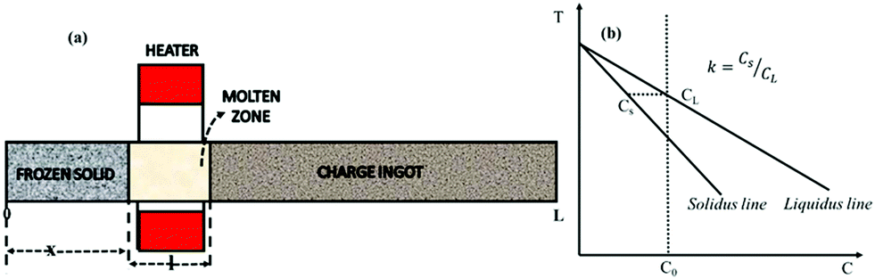
Initially, in the 1970s when Si–Ge was considered the only high temperature thermoelectric alloy for space missions, the evaluation of its thermoelectric properties was promising, and thus, the preparation of good quality samples was critical. At the first stage of investigating the material, a single crystal or large grain polycrystalline ingot was synthesized.26 Since Si–Ge is a completely miscible system, therefore, in principle, Si–Ge crystals with desired Ge contents can be realized. The phase diagram presents opportunities to engineers and scientists worldwide to manipulate the material properties and increase the device efficiency by including Si–Ge in Si.27,28 However, crystal growth expertise has not yet been established for single crystalline Si–Ge bulk crystal having homogeneous Ge content from liquefied Si–Ge. This can be attributed to the inherent complications of controlling the Ge content and circumventing polycrystallization from molten Si–Ge during bulk crystal growth. The phase diagram of Si–Ge, as indicated in Fig. 1, is very straightforward with one solidus and liquidus line. These two lines intersect at the freezing points of Ge (938 °C) and Si (1414 °C). Usually, the outgrowth from the melt progresses under near-equilibrium conditions, and the solidus line determines the content of Ge in the Si1−xGex crystal, XS, which originate from molten Si–Ge at a given temperature, T.29 Therefore, the manipulation of the growth parameters is very crucial, especially T with a steady value to attain consistent Ge content. Moreover, the high distribution coefficient of Si in Ge (κGeSi ≈ 5) creates problems in developing SiGe single crystals from the melt and the considerable difference among the melting points of Ge (∼938 °C) and Si (∼1414 °C) tends toward constitutional supercooling.30 Supercooling can be avoided by high temperature gradients at the phase periphery in agreement with the Tiller criterion. Thus, a minor variation in the temperature, ΔT, might cause a considerable disparity in the Ge content, Δxs. Besides, the phase diagram of the binary alloy system Si–Ge illustrates that there is a wide separation between the solidus and liquidus lines at a particular temperature. This implies that the segregation coefficient, k = XS/XL, deviates from unity, and the liquidus Ge content, XL, is greater than the solidus Ge content, XS. Hence, it is obvious that crystal growth will result in the depletion of SiGe; thus, we begin with a predetermined amount of liquefied Si–Ge. Thus, the leading force of the crystal growth vanishes. Hence, there exist two major prerequisites for crystal growth to obtain an Si–Ge bulk crystal with consistent Ge content: (i) to maintain a constant temperature for growth, and (ii) to supply Si in the SiGe melt.29
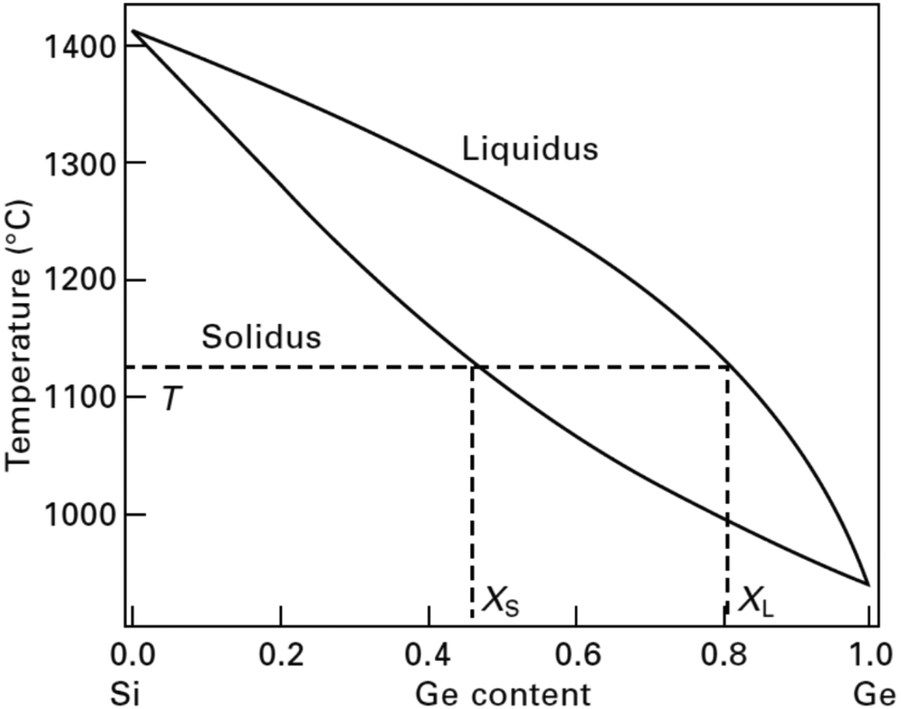 | ||
| Fig. 1 Phase diagram of Si–Ge: at a given temperature T, the presence of Ge in the Si–Ge bulk crystal can be established based on the solidus line. | ||
2. Synthesis methods for Si–Ge alloy using bulk crystal growth
Increasing demand for crystals used in semiconductor physics, engineering, electro-optic devices, etc., has led to the growth of crystals otherwise. In earlier days, natural specimens were the lone source of large, well-formed crystals.31 Crystal growth generally occurs utilizing the following series of processes.• Diffusion of the molecules of the substances to be crystallized through the surrounding atmosphere.
• Molecules diffuse over the surface of the crystal to distinct sites on the surface.
By crystal growth techniques, nowadays, nearly all naturally occurring crystals of interest can be synthesized successfully in the laboratory.32 The growth aspect varies with the crystal depending on their chemical and physical properties such as decomposition, solubility, phase change, and melting point.
2.1. Basics of crystal growth
To grow a crystal, the state of supersaturation, followed by the process of nucleation, is the fundamental condition that needs to be attained.33,342.2. Conditions for growing a crystal
Crystal growth can only occur from pure gases and pure liquids or liquid and gaseous solutions, if a certain degree of supersaturation or supercooling has been initially achieved in the system. The realization of the supersaturated state is vital for any crystallization operation and the extent of super saturation or divergence from the equilibrium saturated condition is the key factor controlling the deposition process.35 The growth of crystals can be considered to take place in the following steps.(1) Attainment of supersaturation or supercooling.
(2) Development of crystal nucleus of microscopic size.
(3) Consecutive growth of crystals to produce distinct faces.
2.3. Crystal growth techniques
Crystal growth is a demanding task and the procedure followed for the growth of the crystal depends on the features of the material under investigation, such as its volatile nature, melting point, and solubility in solvents.36–44 The fundamental growth methods available for crystal growth are broadly classified in accordance with the flow chart,45 as shown in Fig. 2.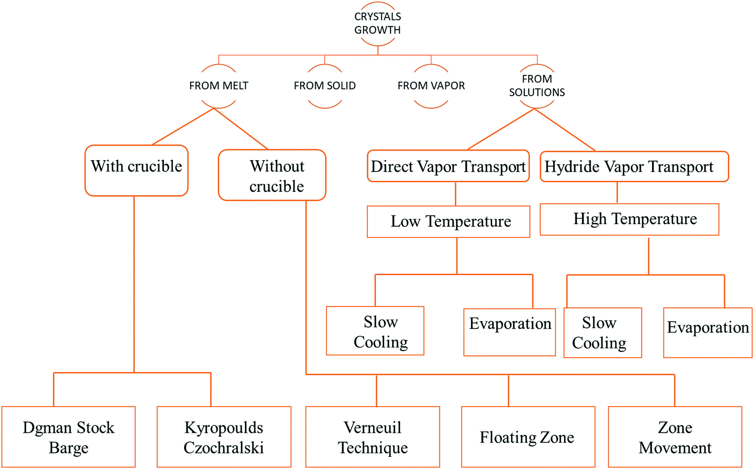 | ||
| Fig. 2 Categorization of crystal growth techniques. | ||
The most common techniques that have been adapted are as follows.
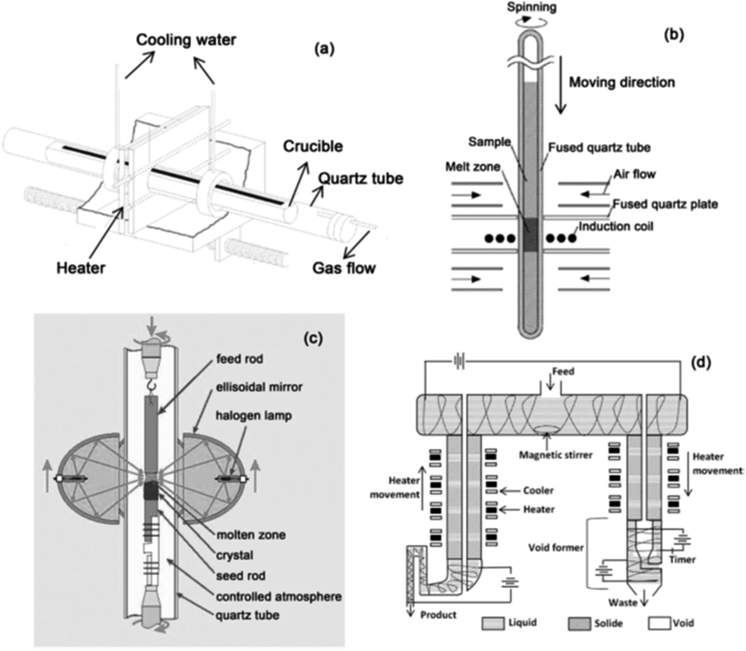
(i) Bridgman method. In essence, the Bridgman Method, as shown in Fig. 3, produces crystals from flux by gradually freezing it from one end to the other. The technique yields crystals with suitable dimensional control and involves little or no supervision due to its simplicity.47,48 However, controlling the heat flow becomes progressively difficult; for instance, the diameter of the crystal enlarges. A broad variety of materials are formed using this method. One major requirement is that the crucible material should remain intact either from the melt or its vapor. Dislocation densities can also be restricted to >104 cm−2, and many materials comprise grain boundaries with a low angle. Because the Si–Ge phase diagram depicts that it undergoes strong segregation in the course of growth, the synthesis of the alloy is not straightforward. The convection current occurring within the molten Si1−xGex causes fluctuations within the growth parameters.49 Moreover, due to the massive density difference of molten Si and Ge, gravity plays a key role in the stimulation of convection movements in the liquefied alloy. This indicates the significance of Si–Ge crystal growth on an extended interval microgravity stage to unearth its basic properties. Concerning the planning of likewise experiments, the growth of SixGe1−x crystal with x = 0.25 and 0.15 was performed by means of the vertical Bridgman technique within the test site. The expansion was carried out in a 3-zone resistive furnace comprising of Pt–Rh heating wire. The expansion ampoules were moved at a pace of 0.3 mm h−1 and 0.4 mm h−1, where the slope was alongside the g vector. The developed Si–Ge samples were measured to be 9 cm long and 2.5 cm in diameter. The samples were carved axially, polished, and etched to review the growth of the expansion patterns along the axis of expansion. The interface profile transformed from concave to planar or convex as the growth progressed. Microprobe analysis using electron microscopy was dispensed to live the Si content beside and transverse to the axis of expansion. The axial Si content was analyzed employing a simple 1-D model, considering full amalgamation of the melt in the course of growth and a segregation coefficient that differs in the Si content within the flux, as given by the phase diagram of the Si–Ge alloy.50,51
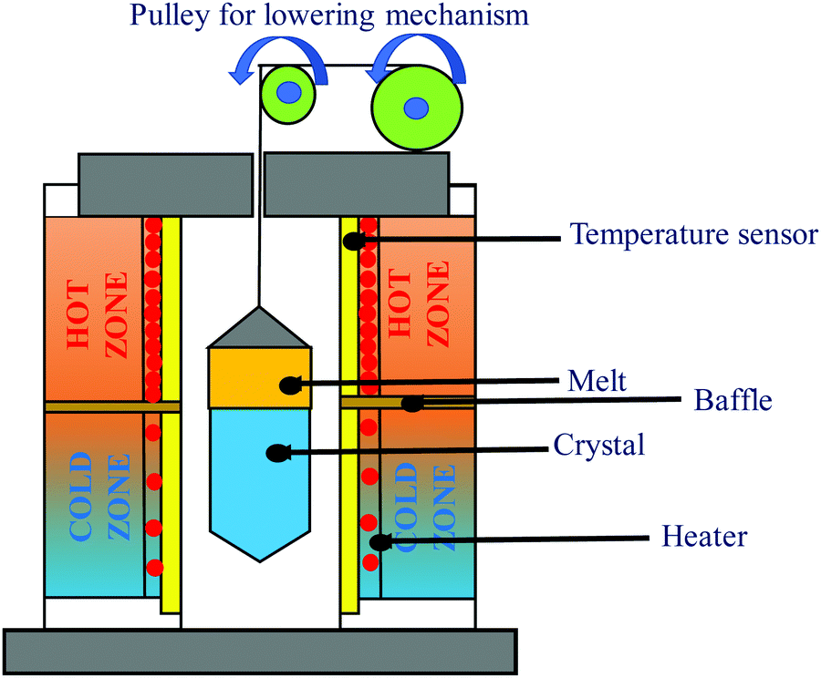 | ||
| Fig. 3 Schematic of the Bridgman method. | ||
(ii) Czochoralski method. This technique may be a workhorse for the synthesis of an overwhelming majority of Si single crystals to date. Thus, several researchers have applied the CZ method, as shown in Fig. 4(a), to get single crystal Si–Ge. The technique is known after the renowned scientist Jan Czochralski from Poland, who developed it in 1916.52 However, numerous intrinsic difficulties are related to the growth of the single crystal from the melt having multi-elements such as Si–Ge in divergence to the growth of a crystal of a single element.53 Freidrich et al. illustrated that probability of existence of “structure loss”, i.e., presence of dislocations and grain boundaries increases the manifold by CZ growers thanks to the high concentration of doping; therefore, the phenomenon is often termed as “constitutional supercooling”.54 The phenomenological description of constitutional supercooling can be described by Fig. 4(b). However, it is applicable to materials that melt congruently or nearly congruently. To realize a stable liquid–solid interface, Kürten et al. reported the CZ growth of Si-enriched Si–Ge by means of a very sluggish pulling rate.55 Deitch et al. explained that the phase diagram of Si–Ge dictates that to avoid the onset of dendritic growth, an extremely low pulling rate is required.56 Thus, the synthesis of the Si–Ge bulk crystal by the CZ method is 40 times slower than the traditional CZ method of the synthesis of the Si bulk crystal. Abrosimov et al. used Si rods for the continuous feeding of Si to the melt so as to avoid the depletion of Si during CZ growth.57 As a result, single crystalline Si–Ge having Ge ≤ 0.2 was attained. Kurten and Schilz produced Si–Ge alloys having 0.62 < x < 0.9855 using the heteroseeding process, where the seeding material is either Si or Ge crystals. Usually, the Si seed is employed aiming at the production of Si–Ge single crystal even from the original melt of pure Ge. The heterocrystal is created by considering Si element in the molten seed of Si. Hence, for the entire composition range of x = 0–1, Si seed is understood to be available for the growth of Si–Ge crystals.58 Based on Tiller's criterion,59 Yonenaga et al. estimated the critical growth velocity of the occurrence of constitutional supercooling as a function of Ge content at a given ΔT.53 However, polycrystallization was observed for the intermediate Ge content, even when the expansion velocity is slower than the critical value. Fig. 5(a–c) demonstrates the Si and Si–Ge crystals grown by the CZ method.
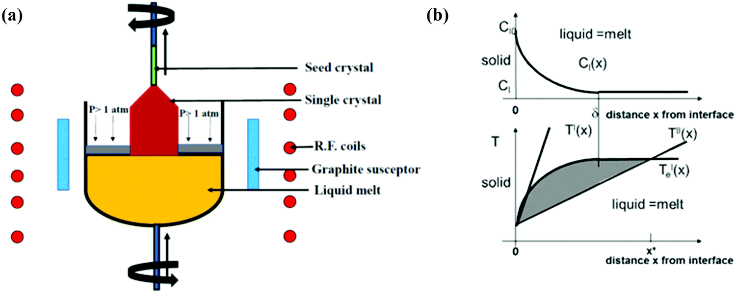 | ||
| Fig. 4 (a) Representation of the Czochralski method and (b) distribution of the concentration CL(x) of a dopant within the melt versus distance x from the expansion interface, where CL(0) denotes the concentration within the melt when no distance is traversed from the interface. δ signifies the width of the physical phenomenon. Liquidus temperature T′e(x) resembling the concentration profile CL(x) plotted in (a) versus distance x from the expansion interface, plotted within the same scaling as in (a). The temperature profiles T′(x) and T′′(x) are two cases that show two different designs of the new zone or the heating conditions in an exceedingly certain CZ growth setup. The shaded area indicates the zone where the melt is “constitutionally supercooled” before the expansion interface, reaching up to position x* within the case of temperature profile T′′(x). Reproduced with permission from ref. 54. | ||
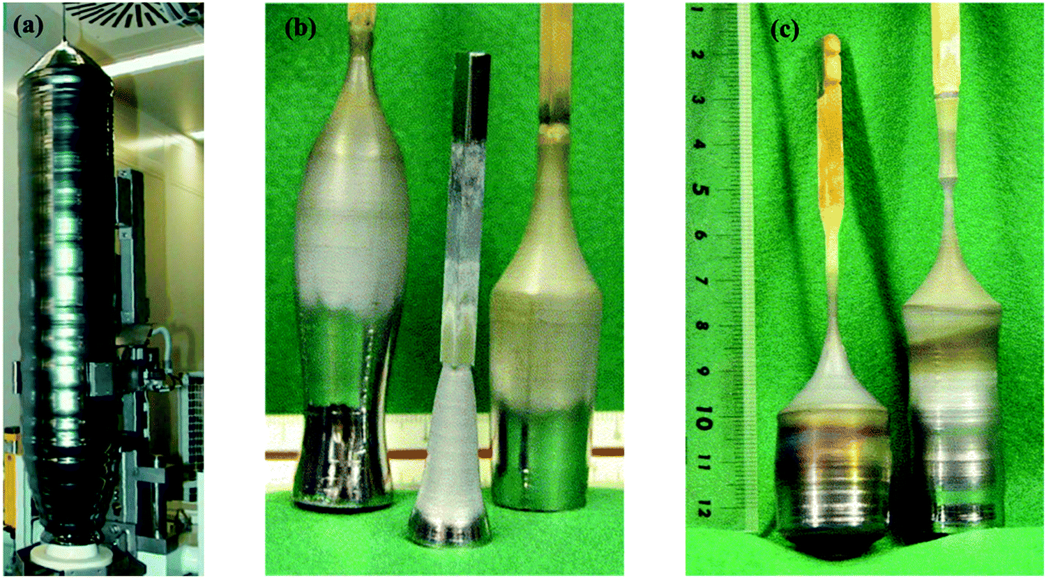 | ||
| Fig. 5 (a) Silicon crystal having a radius of 150 mm and a weight above 250 kg, grown by the CZ technique (Image courtesy of Siltronic AG4), (b) SixGe1−x alloys developed by the CZ method having [001] oriented Si seed crystal. (c) GeSi boules developed with Dash necking (left) and developed with a Si–Ge seed with identical constituents (right). Reproduced with permission from ref. 53. | ||
(iii) Zone melting. The word ‘zone melting’ symbolizes a genus of techniques for regulating the impurities or solute concentrations in crystalline materials, which was first pioneered by Pfann60 to purify Ge for its use in transistors.61 It will be employed to enhance the impurity segregation by offering a high degree of separation of the solvent and solute, which is termed as zone refining, or to get rid of segregation by offering a standardized distribution of impurity within the material, which is known as zone levelling. Zone refining is an exceptionally efficient purification method that utilizes combined melting and freezing practices for refining semiconductors, metals, and inorganic and organic chemicals.60,62,63 Here, a narrow molten zone is allowed to navigate across a solid bar by concentrating and progressing a source of warmth at a specified rate along the matter having both melting and solidifying liquid interfaces, as shown in Fig. 6(a and b). At the edge of melting, solid matters are liquefied and blended including the contents of the molten region. However, at the interface of freezing, the impurities within the recent frozen solid varies as of that within the liquid. However, if the impurity reduces the freezing temperature of the solvent, the freezing interface continuously discharge the solute atoms into the molten zone where they bring together and are propelled toward the intense end of the bar, i.e., within the similar direction of the zone movement. Nevertheless, if the solute increases the temperature of the solvent, the build-up of the solute within the solidifying interface is going to be preferred, thus offering a progressive purification within the reverse direction of that of the zone movement. Thus, the interface of freezing can attract or reject selected kinds of solutes, leading to better-purified materials. Zone refining seeks suitable application in synthesizing silicon-on-insulator (SOI) films64–67 and ultra-pure materials68–74 as super-conducting and semi-conducting75–78 substances.
 | ||
| Fig. 6 Schematic of (a) the zone melting method; (b) a part of binary phase diagram. | ||
Based on the above principle, different zone refining technologies exist and, counting on the strategy of charging and also the geometry, the categorization will be of four types (Fig. 7), viz., (a) horizontal, (b) vertical, (c) floating, and (d) continuous zone refining. Table 1 summarizes the different ways of zone melting, which comprises detailed characteristics, pros and cons, and operations for each variant.
 | ||
| Fig. 7 Arrangement of technologies involved in variable zone refining: (a) horizontal zone refining set up;79 (b) vertical zone refining set up;80 (c) floating zone refining set up;81 (d) continuous zone refining set up,82 adapted pictures. | ||
| Forms of zone refining | Features | Pros | Cons | Purposes |
|---|---|---|---|---|
| Horizontal zone refining | Crucible is placed horizontally whereas heating elements are moved horizontally | Simple to load and unload the materials, and the interfaces can be distinguished easily | Engage more space | Used for most metals except for some materials that are reactive. |
| Vertical zone refining | Crucible is placed vertically whereas heating elements are moved vertically | Engages small space | It is difficult to load and unload materials and crucibles are at a higher risk of cracking | Used for most metals except for some materials that are reactive |
| Floating zone refining | Deprived of crucible, the stuffs are positioned vertically and the molten zone is retained at the solid–liquid interface | Low contamination, low space occupation, and good transfer of heat | Restricted charging material of high surface tension and low yield due to small size of the material | Used for reactive metals such as silicon, zirconium, tungsten, and iron |
| Continuous zone refining | Inlets and outlets are there for feeding materials and continuous collection of waste and product, respectively | High yield and high refining efficiency | Intricate design, high cost, and inconvenient operation | Hypothetically, most metals but the experimental stage is under development and hence is of no commercial usage |
a. Zone Levelling. As mentioned earlier, zone levelling is unique among several zone melting methodology and is used for high T thermoelectric alloy, viz., Si80Ge20 solid solution, which causes homogeneous distribution of impurities.
The molten zone navigating a block has two solid–liquid interfaces: (i) a melting edge and (ii) a freezing edge. At the melting edge, the melting of the solid ingot initiates and fuses with the matters of the zone and thus separates out, whereas at the freezing edge, the concentration of the solute in the region that is getting solidified differs from that in the liquid.
The two possible conditions that prevail are (i) if the soluble impurities (solute) lower the melting point of the solid charge (solvent), then the concentration of the impurities will be lower in the freezing solid as compared to that in the liquid. Hence, the impurities will be discarded by the freezing solid and expelled with the molten part; (ii) if the contaminant elevates the melting point of the charge solid, then the strength of the impurities in the freezing solid will be high as compared to that in the liquid and thus the liquid will be depleted of impurities. Thus, the freezing interface can expel out certain amounts of impurities.83
Here, the charge consists of two components that constitute a binary solid solution. The composition varies with along the length of the ingot (x). The ingot might contain two rods of pure components whose relative cross-section is decided by the mean composition C0. The length l of the molten zone traverses the charge gradually. When the heater (zone) passes through the ingot, the profile of the distribution of the impurities (solute) is shown in Fig. 8.
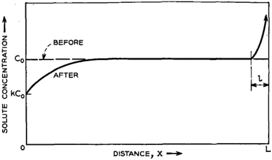 | ||
| Fig. 8 Estimated solute concentration following the movement of the molten zone across the charge of homogeneous mean concentration C0. Adapted from ref. 60. | ||
The curve has been divided into three discrete regions: (i) initial region, (ii) level region, and (iii) final region. At the beginning, the concentration of the melted material is C0. Assuming the efficient distribution coefficient (k) to be less than unity, whilst the zone proceeds a brief distance, it solidifies, at x = 0, a sheet of solid of strength kC0 of the solute, and so persists, at x = l, by liquefying a layer of strength C0. Consequently, the region is enriched and solidifies at a higher concentration. The critical important parameter in this process is the equilibrium diffusion coefficient, k, along with keff. keff is demonstrated to be the ratio of experimental Cs and CL, i.e., Cs/CL. Nevertheless, the difficulty in determining CL experimentally, the Bruton–Prim–Slichter (BPS) equation,84,85 and the model is used to determine keff and is given by 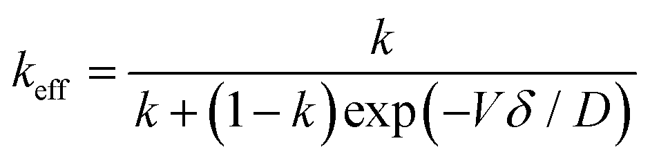 , where V is the velocity of movement of the molten zone, D is the diffusion coefficient of the impurity in the flux, and δ is the width of the boundary of the diffusion layer at the interface of solid/liquid.
In the case of refining of the Si80Ge20 alloy, two precursors of Si–Ge were chosen: a(Si52.5Ge47.5) for zone melting and x(Si80Ge20) for homogeneity, i.e., composition levelling.86 They are preloaded into either the processing boat, which can be made of glassy carbon, carbon-coated quartz, or graphite, which is scaled inside a quartz tube maintained at vacuum, and the zone is melted at a steady temperature. During the passing of zone on both liquid–solid interfaces, two processes take place simultaneously: melting of the pre-synthesized (non-uniform) precursor x, on the interface at the right, and the crystallization of uniform composition x, at the left interface. However, at each fixed time, the amount of the crystallized material and the amount of the molten precursor remains the same. Thus, a fixed composition of the melt is retained, and so a uniform Si80Ge20 solid–solution bar is yielded. In order to evade the relapse of the quartz ampoule, the zone heater made of RF coil is used as an alternative of the typical resistance furnace. Here, the graphite crucible performed the function of an RF susceptor, the complete heating assembly was fixed, and the ampoule was slided. The rate of movement was kept sufficiently low to deliver uniform recrystallization of the charge. Hence, inter-crystalline liquation was averted. It needs to be noted that the overall procedure was accomplished at a temperature much lower than T′liq of Si80Ge20.
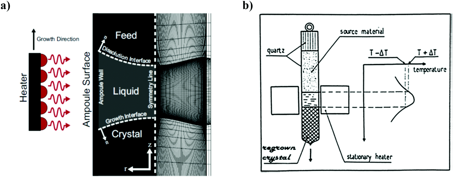
b. Floating zone method. The float zone (FZ) method is a crystal growth technique where a zone of melt is created between the upper feed material and lower seed material by employing restricted heating (Fig. 9).58,87 The starting material of the process consists of a seed crystal and a polycrystalline rod. Using the comparative motion of the heating device, the zone of floating is translated along the length of the rod in such a manner that the growth of the crystal occurs on the seed (which is underneath the melt) and concurrently melts the feed material over the floating zone. Here, unlike the CZ method, the crystal is allowed to grow without any interaction with the wall of the crucible. Thus, the concentration of impurities reduces drastically and high purity crystals are obtained, although the diameter of the crystal is less than 150 mm and the diameter of the ingot is restrained by the surface tension of the molten zone. The technique leads to next-generation saleable crystal products (such as a majority of extremely pure silicon yielded today is administered by the FZ technique).
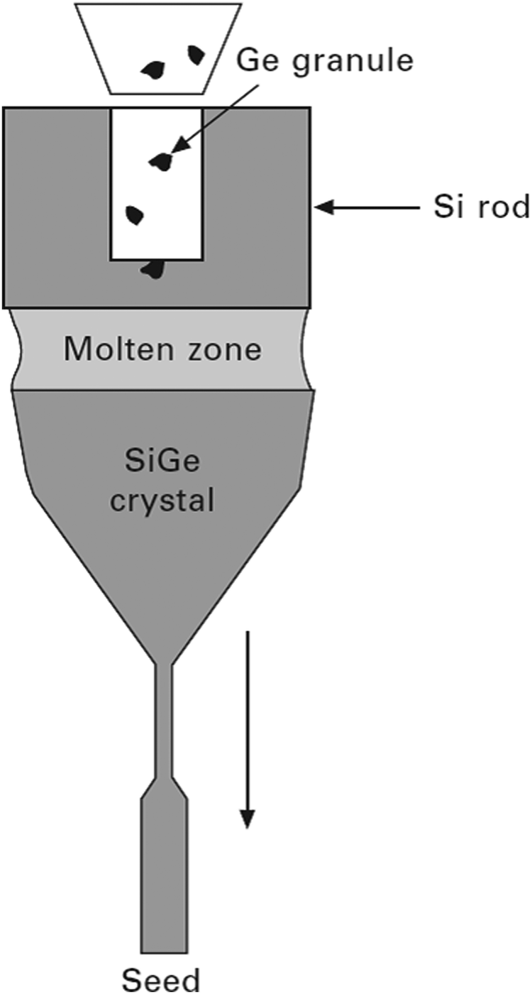 | ||
| Fig. 9 Schematic of FZ growth of the Si–Ge bulk crystal with continuous charging of Ge granules. Adapted from ref. 29. | ||
The benefits of the FZ method for the growth of Si–Ge crystal lies in the fact that there is a sharp temperature gradient to circumvent constitutional supercooling59,88 and the lack of wall contact. Both are beneficial for overcoming polycrystallization. However, it is difficult to feed the base elements in the molten zone because the feed rods are chemically deposited for Si technology and are not accessible for silicon–germanium crystal growth. Thus, a method was adapted for the alloying of Si with Ge, which allocates the enduring feeding of Ge granules (∼3.5 mm3) throughout the process of growth precisely into the melt.89 Saidov et al. explained that to avoid constitutional supercooling, electron beam heating can be used as it creates a temperature profile where the centre of the liquid zone attains the maximum temperature and thus a characteristic temperature gradient is established.87 The obtained single crystal can have Ge up to 50% with an ingot (pre-synthesized polycrystalline Si–Ge) of diameter <3 mm with narrow melting zone. Wollweber et al. worked with the RF-heated FZ equipment for the synthesis of Si1−xGex single crystal,90 whereas Campbell et al. used the mono-ellipsoid mirror furnace in the FZ method to grow Ge-rich Si–Ge crystal.91 The significance of the technique, for the perfection of the Si1−xGex single crystal, has to be credited to the optimized progression parameters, viz., the rate of rotation, the dimension of the RF coil, and the feature of the feeding rod.
c. Liquid encapsulated zone melting (LEZM). Since the bulk crystal growth of uniform composition of Si–Ge alloy is challenging using the conservative method, viz., Bridgman and Czocharlski (CZ), studies that are more recent indicated that the FZ technique is highly suitable, which aims at the synthesis of uniform Si–Ge alloy composition. However, to regulate the composition for growth, the method demands the measured feeding of Ge granules into a Si bar. Advancement toward the experiments have shown that the approach of LEZM can produce a single crystal having a uniform chemical composition, a uniform strength of dopants all through the crystal, and a low and uniform dislocation density. This non-conservative technique portrays the use of CaCl2 as an encapsulate and yields single crystal of a constant composition.92,93
An RF furnace with a vertical tube geometry has been tailored with a concentrator coil having a water-cooled jacket for zone refining, as depicted in Fig. 10. Theoretically, the coupling amongst the charge and the concentrator needs to be adequate to liquefy the Si charge; however, the limitation from the power source inhibits the melting of the charge immediately. Thus, a susceptor ring of graphite was mounted into the concentrator coil to deliver an uninterrupted supply of radiant heat. The alloy charge and the silicon seed were preloaded into a quartz ampoule, which are precisely attached within the graphite susceptor ring. As shown in Fig. 10, the ampoule was preloaded with a single-crystal seed of silicon at the bottom; subsequently, a disk of pure Ge and, afterward, a cylindrical bar of pre-synthesized Si–Ge alloy. The encapsulant CaCl2 was positioned above the charge such that it covers the internal region of the quartz ampoule as soon as the melting is initiated. A fiber optic thermometer system is used to monitor the temperature profile of the zone melting system. A fiber was placed into quartz tube at the centre of the pre-pierced Si–Ge charge, and the recorded temperature was documented while the fiber was detached from the hot zone at a speed of few mm h−1. Thus, the sapphire fiber treated at the tip with a thin layer of refractory metal was employed to determine the temperature of the alloy charge and from the seed through the molten zone.94
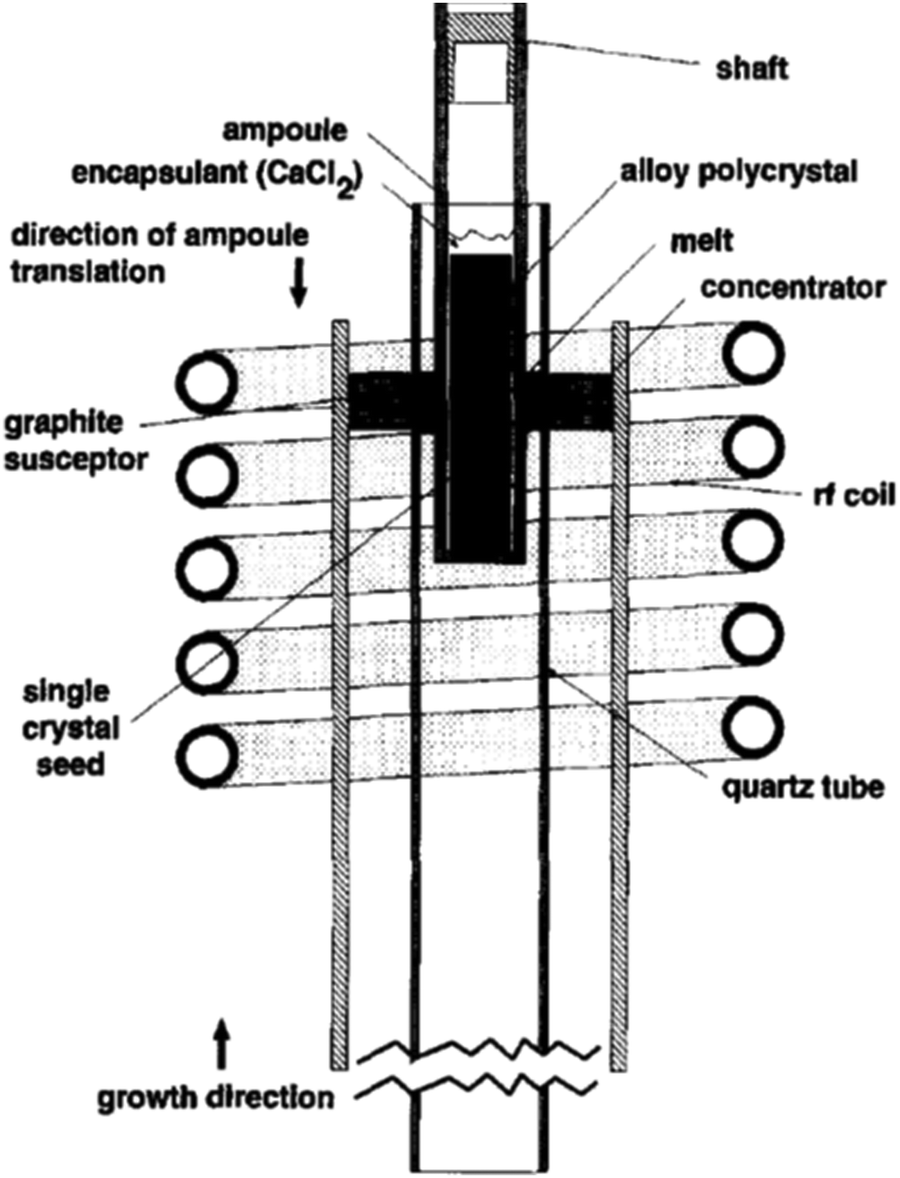 | ||
| Fig. 10 Liquid-encapsulated zone melting growth set up. Reproduced with permission from ref. 93. | ||
Thus, the LEZM technique proved to be a useful elucidation of two glitches related with the growth of single crystals of non-congruently melting alloys. Formerly, the liquid encapsulant minimizes the adhesion difficulty, reduces the reaction among the container and the melt, and regulates nucleation. In addition, the liquefied zone method regulates the compositional homogeneity of the entire solid solution.
d. Multicomponent zone melting methods. Aimed at the growth of multicomponent semiconductors, Nakajima et al. and Suzuki et al. recommended the “multicomponent zone melting method” where the constituents are entirely soluble in the solid state.95 This method satisfies two requirements, i.e., to attain uniform alloy content in the development of binary and ternary compositionally graded bulk crystals.96–99 Yonenaga and Murakami et al. could attain Si-rich SiyGe1−y bulk crystals having a homogeneous composition with y = 0.03 and 0.07 and with a length of 10 mm but without the introduction of feeding methods, which compensates the depletion of silicon solute elements during compositional alteration into the crystals.100 To elucidate the influence of depleted solute elements of Si, two types of methods were adapted to grow the bulk crystals of Si-rich SiGe. Fig. 11(a and b) demonstrate the arrangements of the quartz crucible with growth materials both prior to and during growth along with temperature programming in the furnace.
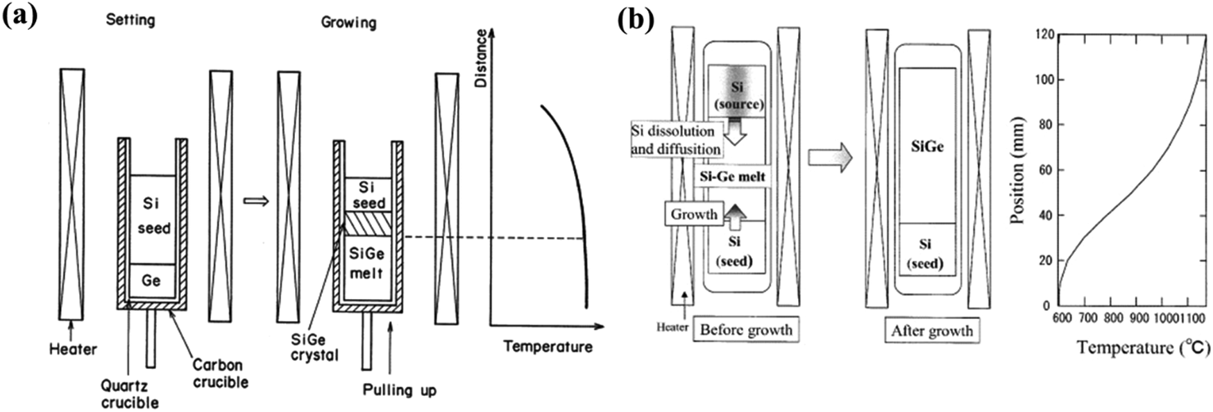 | ||
| Fig. 11 Quartz crucible with growth materials before and throughout growth, and the temperature outline inside the furnace. (a) Without any means of supply of depleted Si solute elements. (b) With supply means of depleted solute elements of Si. Reproduced from ref. 95. | ||
Here, in Fig. 11(a), single crystals of Si and Ge were loaded in the quartz crucible and placed inside the graphite crucible. Temperature programming inside the furnace contains both a constant and a gradient zone. The carbon crucible was rotated to ensure consistent temperature profile perpendicular to the growth direction. Initially, portions of both Si and Ge crystals were liquefied and the solute element, i.e., Si from the single crystal diffuses into the molten Ge to create binary Si–Ge melt. Prior to the withdrawal of the crucible, the binary melt is almost uniform and the composition of the molten alloy is dictated by the equilibrium composition of the melt, which is in proximity to the Si crystal at the interfacial temperature. During growth, the Si solute atoms unceasingly diffuse toward the interface of the Si–Ge binary melt and the subsequent supersaturation drives the growth of the crystal. Thus, the composition of Si in the melt decreases gradually. The Si crystal serves twofold purposes: (i) source material and (ii) seed.
Fig. 11(b) shows the growth of Si–Ge bulk crystals where temperature programming has a constant temperature zone and a fast-cooling zone with substantial temperature gradient. The method involves incessant stock of Si from the basis crystal for the binary growth of Si–Ge from the melt. Two Si single crystals and polycrystalline Ge crystals are placed in a quartz crucible airtight in a quartz ampoule maintained at high vacuum. With the onset of the melting of a portion of the two Si crystals (both source and seed) and Ge crystal, the growth is initiated to form a binary growth melt of Si–Ge. In the melt, the diffusion of the Si atoms is initiated from the source crystal to the seed crystal due to the gradient of concentration of Si developed due to the temperature difference. The growth arrangement was heated up to 1453 K rapidly. For the growth, the geometry of the Si and Ge crystals was controlled to pin the temperature at the interface at 1373 K. In this technique, the Si seed crystal was not melted and the crucible was not pulled during the growth of the crystal. Rather, the method adapts the cooling of the growth system by rapid quenching.
iv. Traveling solvent technique. Travelling solvent technique is an influential and versatile method and is related to the growth of crystals, especially for materials that are difficult to melt owing to phase transformations or decomposition.101 There are two main alternatives: the first approach, the travelling solvent method (TSM), is particularly applicable for thin perfect crystal growth and single-crystal rectifying junctions, and the second approach, THM is beneficial for the development of bulk single crystals, where it diminishes the detrimental outcome of constitutional supercooling.102a,b In brief, the latter approach is extremely effective for solid solutions of uniform composition and of peritectic compounds.83 The liquid zone softens and melts the polycrystalline feed at its upper interface with high T and deposits, with approximately similar composition at the lower interface with low T, in near equilibrium conditions.103–105 The method is capable of removing both dislocations and impurities. This process resembles that of zone levelling, where through a dilute solution, the recrystallization of a concentrated solution occurs and is usually performed vertically with a single pass of the liquefied zone.102 The schematic and the principle of the technique is shown in Fig. 12. Solvents such as Ga and Sn were frequently used for the bulk ingots of Si80Ge20, having growth temperatures between 800 and 900 °C (in comparison to T′liq′ = 1350 °C for Si80Gc20).
 | ||
| Fig. 12 (a) Left: Representation of the travelling heater method (THM). The heater moves in the upward direction of growth. Right hand side shows the finite element mesh representing 90 axial and radial elements within the liquid zone having a higher density of elements at the boundary. (b) Principle of the travelling heater method. Reproduced with permission from ref. 102 (a) and ref. 102 (b). | ||
Thus, THM is a complicated skill requiring the regulation of several technological parameters such as radiant heating, radius of the ampoule and wall thickness of the ampoule, pulling system, fine-tuning of the basis material in the ampoule, as well as ground and temperature stability. Amongst all, a considerable requirement is the suitable temperature programming of the growth furnace. It should produce a narrow molten zone having a sharp temperature peak (approximately of dimension equals to the diameter of the ampoule) and a well-defined temperature difference at the growth interface to counteract constitutional supercooling.
A consolidation of all the single crystal growth techniques is shown in Table 2. This table envisages the technology complexity, sample qualities, and desired applications of different melt growth methods.
| Crystal growth techniques | Technology complexity | Sample qualities | Desired applications | |
|---|---|---|---|---|
| Melt growth method | Bridgman method | • Controlling heat flow becomes progressively difficult as the diameter of the crystal enlarges | • Synthesis of the single crystal ingots with homogeneous composition is not straightforward owing to the massive density difference of molten Si and Ge | Widely used for the synthesis of GaAs single crystal in the semiconductor industry |
| • The method can reliably yield but does not essentially result in homogeneous properties throughout the crystal | • The vertical Bridgman technique enables the growth of crystals in circular shape, whereas horizontal Bridgman technique grows D-shaped ingots. Nevertheless, the horizontally grown crystals show high crystallinity, i.e., low dislocation density as the crystal undergoes lesser stress owing to the open surface present at the top of the melt and can be expanded in the entire process of growth | |||
| Czochoralski method | • Growth of single crystal from melt having multi-elements such as Si–Ge are related to the existence of “structure loss”, i.e., enhancement in the presence of dislocations and grain boundaries and so, extremely low pulling rate is required | SixGe1−x alloys developed having [001] oriented Si seed crystal | Workhorse for the synthesis of overwhelming majority Si single crystal. | |
| Zone refining | • Engage more space | Exceptionally efficient purified alloy is obtained | Silicon-on-insulator (SOI) films, ultra-pure materials, Superconducting and semiconducting substances | |
| • Difficult to load and unload materials and crucibles | ||||
| • Intricate design and high cost of operation | ||||
| Traveling solvent technique | • Complicated skill requiring the regulation of several technological parameters such as radiant heating, radius and wall thickness of the ampoule, pulling system, fine-tuning of the basis material in the ampoule, as well as ground and temperature stability | Efficient for the growth of crystals, especially for materials possessing difficulty in melting due to phase transformations or decompositions. It diminishes the detrimental outcome of constitutional supercooling | Growth of Si, Ge, and GaAs crystals |
(i) Liquid phase epitaxy. In liquid phase epitaxy (LPE), the solution remains in a growth cell, which is generally a rectangular cavity.113 The elevated rate of growth in LPE is appropriate for the growth of dense Si–Ge buffer layers with varying composition and forming Si–Ge top layers having thickness above 20 μm, which is suitable for generating SiGe-on-Si epitaxial virtual substrate. Thus, two-dimensional models provide satisfactorily accurate predictions for most objectives. In this section, the technique presents the simulation models developed for the LPE growth of binary Si–Ge systems.114 Nevertheless, under LPE condition, lattice disparities higher than 1% are identified to restrict the nucleation of epitaxial layers. The schematic of the LPE technique is shown in Fig. 13.
 | ||
| Fig. 13 Representation of the principle of LPE. | ||
In the last few years, LPE has been grown on Si1−xGex or Ge on Si using the fast melt growth method;115 however, the epitaxial areas were restricted to diminished structures and recurrent pre-growth lithographic and deposition handlings were essential. Of late, to deposit strained Si1−xGex layer above the thorough Si(100) substrates in a lone step, a lateral LPE technology has been established. The technique yields either Si1−xGex or Si1−xGex graded buffers. The essence of the film developed by LPE on an average shows low dislocation densities in comparison to other techniques, viz., molecular beam epitaxy (MBE) and chemical vapor deposition (CVD), due to growth in proximity to the equilibrium, which makes dislocation nucleation difficult. Moreover, LPE encompasses low investment, high rate of growth than MBE and CVD, and is less toxic than CVD.116
(ii) Molecular beam epitaxy. In this epitaxial process, materials are grown under ultra-high vacuum (UHV) conditions on a pre-heated crystalline substrate using the reaction of the adsorbed species provided by atomic or molecular beams.117–119 The layers possess (i) a structure with analogous symmetry or comparable crystalline structure of the substrate and (ii) a lattice parameter of the film deposited; the substrate should differ by less than ∼10%. In general, the beams contain thermal energy and are formed by the sublimation/evaporation of suitable constituents placed in ultrapure crucibles.120,121
The method is extensively applied for the formation of not only single thin films but also multilayers of semiconductors and metallic materials. In this technique, since the growth occurs under an UHV condition, i.e., of the order of 10−8 Pa, the growth rate can be slowed to a sub-nanometer scale thickness per second. Thus, the method has great potential for producing wide varieties of nanostructures such as quantum dots, multi stacking atomic layers, and nanowires.122
In this section, we focus on MBE as a tool (Fig. 14) for the formation of nanostructures made with Si–Ge and related materials. A strain-relaxed Si–Ge layer on Si is a model structure for technological applications. The technique is perhaps the most accepted method for Si/SiGe growth in academia and research labs. MBE is essentially a physical-vapor deposition procedure, provided the development of the layer is via the direct evaporation of Si and Ge (from ultrapure solid sources) simultaneously, along with the coveted additives under UHV conditions. The straight impingement of the constituent elements on a hot substrate alters the evaporants to a supersaturated state, which is concentrated, followed by nucleation and growth. Thus, in accordance to the first-order approximation, the rate of growth is independent of the orientation of the substrate; however, it depends weakly on the substrate temperature. Recently, Si/SiGe heterostructures were successfully grown using MBE systems with gas sources.123
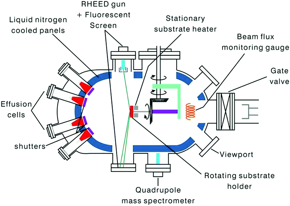 | ||
| Fig. 14 Schematic of the principle of MBE. | ||
During epitaxy, dopants are normally added into the film by low-energy ion implantation using an effusion cell by evaporation.124,125 In few instances, ion implantation cannot be used for doping as the Si–Ge films may undergo damage due to induction by ion source. However, in such cases, evaporation by solid source is beneficial, and mostly Ga is used as the p-type dopant while the Sb is chosen as the n-type dopant, considering the vapor pressure of the dopants.126 Exclusive effusion cells of boron, which illustrates good doping outlines and device characteristics for HBTs of B-doped SiGe, have also been prepared.127 Thus, MBE can cause very rapid changes in the dopant profiles as the shutters right next to the effusion cells can cause disruption in the dopant fluxes. Some of the inherent probable benefits of MBE in comparison to UHV-CVD for the growth of Si/SiGe heterostructure includes (i) reduced growth temperature, (ii) better regulation of Ge and profile of dopant, (iii) thickness of the film, and (iv) the aptitude to form additional elegant Si-based structures and superlattices (including separator and layers of metal on Si).128
In 1992, the renowned scientists Dresselhaus, Harman, and Venkatasubramanian were the first to propose the concept of superlattices in thermoelectric research.109 Superlattices are defined as multilayer structures where two different materials grow by turn and the depth of the layer is at the nanometer scale. There is a noteworthy disparity amongst the conductivity of the layers, where one serves as a conduction layer and, subsequently, the other behaves as a barrier layer. Although different techniques are available to prepare the superlattices, MBE was found to be the finest way to obtain well-defined interfaces despite being expensive and having reduced efficiency.111
In the superlattice, the exceptional arrangement alongwith the band alignment, leads to progress in ZT. In accordance to the quantum confinement effect,129 with the existence of nanostructure, the DOS varies as shown in Fig. 15(a) and the patterns of carrier compartments can be determined from the dispersal of DOS, which is represented in Fig. 15(b).
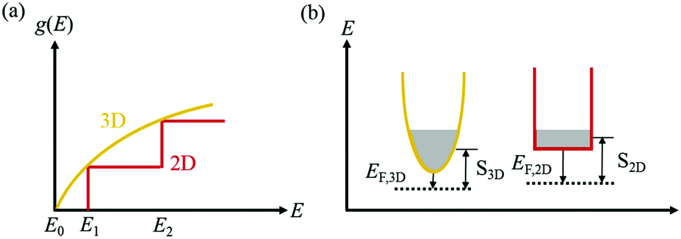 | ||
| Fig. 15 (a) Arrangements of density-of-states (DOS) and (b) carrier compartments in 3-D bulk materials and 2-D quantum-well materials. The width of the conduction valley in (b) signifies the DOS. Reproduced with permission from ref. 111. | ||
The idea of carrier pocket/compartment engineering, first suggested by Koga et al.,130 utilizes the confinement effects, whereby the zT is improved owing to the enhancement in the DOS by exploiting the decreasing dimensionality. This technique is employed to enhance the number of active conduction valleys specifically. Fig. 16 demonstrates the failure of the confinement problem in common multilayer structure in Si and Ge. Since the X-pocket is energetically low, electrons prefer to fill the X-pocket instead of the L-pocket. However, as the depth of the Si- and Ge-layer decreases, the effect of confinement arises and the structure of the carrier pocket differs from the bulk materials.131
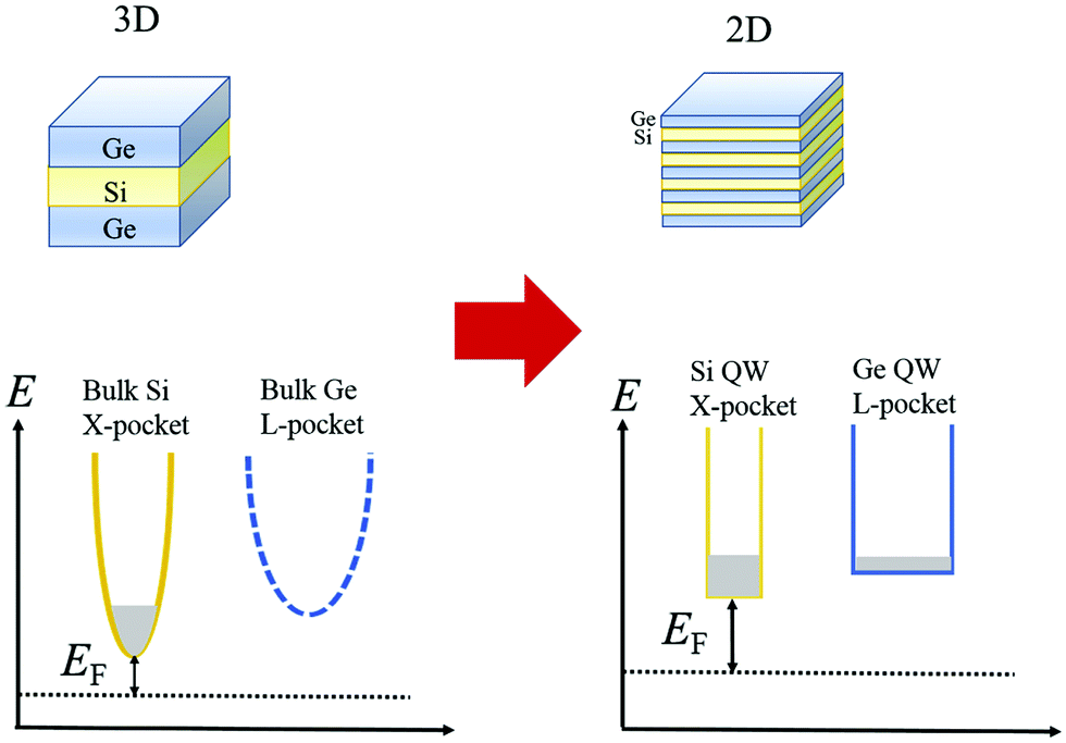 | ||
| Fig. 16 Configurations of the carrier pocket in the Si/Ge multilayer. The lower energy X-pocket is occupied by most of the electrons in the 3D structure. Nevertheless, in quantum well superlattices (2D structure), the energy separation between the X-pocket and L-pocket diminishes due to enhanced confinement energy in the X-pocket (Ec,x > Ec,L) to the L-pocket. Occupancy of both the pockets by electrons increases the DOS, reduced the EF, and enhances the Seebeck coefficient. Reproduced with permission from ref. 111. | ||
However, the disadvantages associated with MBE are (i) lower output compared with the UHV-CVD technique; for mass production, definite levels of quantity are required. (ii) Undesirable contamination due to the chemisorbed oxygen or carbon from the substrate132 or from the residual gas impingement, which demand the cleaning of the substrate in situ prior to the deposition or a dip in the HF solution as an effective cleaning method.133
(iii) Vapor deposition. Vapor deposition or evaporation is a coating process where the substrate to be coated is hanged over the evaporation source and the precursor powders are heated until the vapor pressure is sufficient to smear under high vacuum. The deposition of thin films on varying substrate occurs via (i) physical vapor deposition (PVD);134–137 and (ii) chemical vapor deposition (CVD),138–143 where the vapor states are either condensed through condensation or chemical reaction. The technique is beneficial for being able to increase the deposition technique effortlessly and allocates a better control on the thickness of the film with homogeneous film morphology.
In PVD, atom-by-atom or molecule-by-molecule relocation of material occurs from the solid phase to the vapor phase, resulting in deposition on the substrates. Ion implantation, vacuum evaporation, and sputtering are the most notable techniques used in PVD.
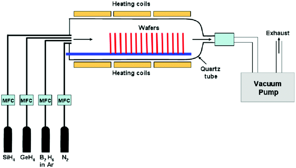
On the other hand, CVD uses a chemical reaction to form a coating from a vapor, with the reaction by-products leaving as volatile species. High temperature is needed for CVD to initiate the chemical reaction. Kunhe et al. described the chemical vapor deposition of epitaxial SiGe-layers from SiH4, GeH4, H2, and HCl gas mixtures at atmospheric pressure.144 Kazmi et al. described that amongst a myriad of practices from various research groups, the low pressure chemical vapor deposition (LPCVD) technique for poly SiGe films deposition is believed to be superior and most extensively used to other deposition techniques due to reproducibility, uniformity, and its higher throughput with a setback of low deposition rate (2–30 nm).145 The plasma enhanced chemical vapor deposition (PECVD) technique is an alternate of LPCVD if high deposition rate, an order of magnitude higher, is required with a compromise on the uniformity and throughput for a conformal deposition.146
In this technique, as reported by Kazmi et al., poly Si1−xGex was deposited on SiO2 surface with a thin layer of amorphous silicon. B-doped poly Si1−xGex layer was deposited in situ using conventional LPCVD from the pyrolysis of pure silane (SiH4) and pure germane (GeH4) gases with 0.2% diborane (B2H6) diluted in argon gas (Ar) as a dopant precursor (Fig. 17). The experiments were executed at varying B2H6 mixture flow rates of 0, 50, and 100 sccm with preset SiH4 to GeH4 ratio (75![[thin space (1/6-em)]](https://www.rsc.org/images/entities/char_2009.gif) :37) and the deposition time of 70 min to originally check for the dopant distribution and Si and Ge contents in the thorough thickness of the deposited layers.
:37) and the deposition time of 70 min to originally check for the dopant distribution and Si and Ge contents in the thorough thickness of the deposited layers.
 | ||
| Fig. 17 Schematic view of the LPCVD system. | ||
Dutartre et al. mentioned that rapid thermal chemical vapor deposition (RTCVD) can be used to grow silicon and Si1−xGex structures at a low temperature using SiH4 and GeH4 in an H2 ambient.147 Haratmann et al. in their detailed review reported about Reduced Pressure-Chemical Vapor Deposition (RP-CVD) for the growth of Si/SiGe heterostructures for nanoelectronics. In this technique, pure silane or dichlorosilane are used as Si gaseous precursors (SiH2Cl2 for (SEG) ⇔ SiH4 for Non-Selective Epitaxial Growth (NSEG)). Germane (GeH4) and mono-methysilane (SiH3CH3) diluted at 2% and 5% in H2 are used as Ge and C gaseous precursors.148 For n-type and p-type doping, phosphine (PH3) and diborane (B2H6), with concentrations in H2 between 5 and 2000 ppm, were chosen. Pure gaseous HCl can be added to the gaseous mixture in order to promote selectivity versus SiO2 or Si3N4. To clean at high temperature and pressure, large flows of HCl were used in between wafers at the inner surfaces of the chamber quartz domes. Finally, very high purity H2 in adequate quantity was used as the carrier gas.
(iv) Sputtering. Although polycrystalline Si1−xGex films were frequently synthesized by means of CVD, RF sputtering (Fig. 18), followed by annealing, offers a trouble-free, inexpensive, and ecofriendly fabrication method. Si1−xGex films deposited using this technique are amorphous, which crystallizes under different annealing conditions.
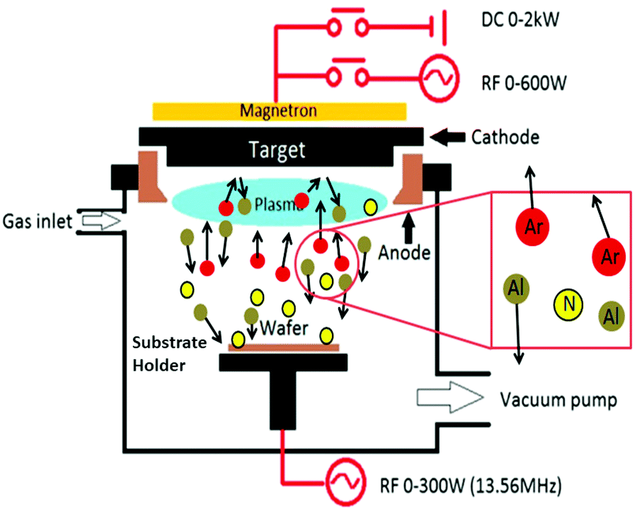 | ||
| Fig. 18 Schematics of the RF sputtering system. | ||
RF sputter deposition involves a network-harmonized current source at a customary frequency of 13.56 MHz and is frequently used through the cathode-anode space. By persistently reversing the positive ions or negative electrons reaching on it, the RF power source prevents the accumulation of charges on top of the insulating materials. Moreover, the oscillatory motion of the electron is discriminately increased by the RF power (due to its smaller mass vs. the heavier ions in the plasma) throughout the chamber. The impact-ionization rate is thus recovered and causes higher plasma density. This methodology is usually employed to attain sputtering rates at high-speed and insulating materials.149,150 Here, the anode is generally connected to the walls of the chamber to enhance the effectual area of the anode. However, a larger voltage drop occurs at the cathode (source) if the effective area for the anode is large; thus, a majority of the sputtering will take place on the source.
Choi et al. in his report explained about the deposition of Si1−xGex films of four different stoichiometries, Si0.37Ge0.63, Si0.40Ge0.60, Si0.72Ge0.28 and Si0.87Ge0.13. In order to deposit amorphous Si1−xGex films on 〈100〉 Si wafers (p-type) having a thin layer oxide grown thermally, the RF sputtering system was employed. Intrinsic Ge pieces affixed to a 4-in. n-type Si wafer were used as a sputtering target. Here, the Ge fraction was regulated by the comparative surface areas of Ge and Si subjected to argon plasma. The RF power employed was 150 W and sputtering and base pressure were maintained at 1 × 10⁻² and 1 × 10⁻⁶ torr, respectively. The as-deposited films were crystallized in an N2 ambience at an annealing temperature between 600 °C to 900 °C kept for 24 h.151
Sasaki et al. explained the epitaxial growth of Si–Ge thin films using sputtering by ion-beam on the Si(100) substrate, as shown in Fig. 19. Using the alternate sputtering method, SiGe films were synthesized by layer-after-layer sequence. A rotatable target system was adapted to prepare multilayer structure and in situ doping. Substrate preheating is essential to initiate the deposition. Si1−xGex films were synthesized using the sputtering of the targets of Si and Ge interchangeably. During the target rotation, the shutter interrupts the Ar ion-beam for approx. 10 s. However, by regulating the sputtering time, the thickness and the average composition of the film can be determined.152,153
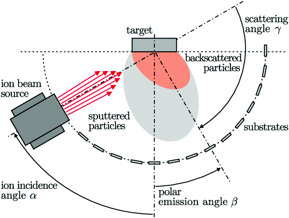 | ||
| Fig. 19 Representation of the ion-beam sputtering system. | ||
A consolidation of all the thin film growth techniques is shown in Table 3. This table envisages the growth methods, technology complexity, sample qualities, and desired applications of different thin film growth techniques.
| Thin film growth techniques | Technology complexity | Sample qualities | Desired applications | |
|---|---|---|---|---|
| Thin film growth method | Liquid phase epitaxy (LPE) | • This growth method under near-equilibrium causes poor control on the thickness of layer and toil in yielding layers having thickness in sub-0.1 μm | Crystals developed by LPE displays 3-dimensional and edge effects in the areas in proximity to the wall of the crucible. Otherwise, LPE process generally produces flat and homogeneous crystalline layers. Thus, 2D-models offer moderately exact predictions for most purposes | III–V solar cells, semiconductor devices such as LEDs, semiconductor lasers, and HBTs, were developed with LPE. The technique is also used for the growth of ferrites, oxides, garnets superconductors, II–VI semiconductors, and II–V compounds |
| • Incompatibility with the development of several heterostructures owing to mismatch in lattices or non-equilibrium conditions amid underlying seeding | ||||
| Molecular beam epitaxy (MBE) | • The significant complexity includes the necessity for high-volume pumping, diminished uniformity, and high-complicated surface chemistry, comprising the demand to pre-crack several precursor molecules | Well appropriate for the growth of superior structures having the profile of doping and composition regulated at the 10−9 scale. This growth mechanism enables the preparation of both less (<2–3%) and extremely lattice-mismatched structures of (1) 2D structures having atomically flat interfaces and (2) 3D nanoislands, which completely restrict the carriers, respectively | MBE can grow crystalline films of extensive kind of materials including Si, II–VI semiconductors, Si–Ge, cuprate superconductors, III–V semiconductors, and metals | |
| • The technique also demands enormously clean ultrahigh-vacuum (UHV) condition in the material growth chamber | ||||
| Vapor deposition | • Method is applied at high temperature | High purity films can be deposited. | Used for the synthesis of a wide range of materials such as semiconductor devices or for coating to enhance the wear and tear of the materials | |
| • Challenging to the mask surface | ||||
| • The reaction chamber capacity dictates the size of the sample | ||||
| • The sample needs to be relocated at the deposition site and so is not an “on site” process | ||||
| Sputtering | • The bombardment site of the target is too small and the rate of deposition is usually low | • Capable of depositing several metals, alloys, insulators, and composites | Widely used by semiconductor industries and for integrated circuits for the deposition of elements (e.g., Ta), compound (e.g., TaN), multilayer (e.g., Ti–Cu–Au), and alloy (e.g., Al:1%Si:1%Cu) | |
| • Damage of the substrate may occur due to ion bombardment or ultraviolet radiation formed by the plasma | • The deposited film is the replica of the target | |||
| • Film quality and step coverage are superior to evaporation | ||||
| • Large targets can deposit a uniformly thick layer over the substrate |
2.4. Strength of binary Si–Ge alloy
Si–Ge technology (Fig. 20(a and b)) has arrived a long way since its fortuitous discovery and commercialization. Subsequently, circuit designers have unearthed that this alloy is more efficient than pristine silicon in terms of performance and power consumption, while also intensifying the oscillating and frequency competences of a device.154–165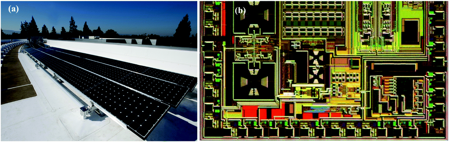 | ||
| Fig. 20 (a) Si–Ge solar panels (image courtesy NASA), (b) Si–Ge chips (image courtesy IBM). | ||
Thus, the benefits of Si–Ge include
• Power saving and high performance
• Numerous possible ways of integration
• Reduced size
• Enhanced electronic mobility
• High oscillating and frequency capability
• Overall low component cost
• High temperature thermoelectric performance
The enhanced electronic mobility in Si–Ge in comparison to Si has managed its place in consumer electronics, telecommunication, computer technologies, space, and aerospace devices.
Several architects and scientists consider Si–Ge a crucial material for that “novel technology”, which imparts cutting-edge high efficiency, space-savings, and thermal stability to progress innovations in space, automotive, telecommunications, and solar industries.
a. Space industry. Thermoelectric devices can acquire the largest power range (W) from the waste heat source. Planetary explorations have great aptitude for their usage as a considerable amount of electrical energy is produced. However, serious threat persists because of the use of radioactive materials. Over the past several decades, Si–Ge type alloys have aided as the desired material for thermoelectric conversion in U.S. radioisotope thermoelectric generator (RTG) power systems for deep space planetary voyaging missions. Silicon germanium (SiGe) alloys, since 1976, were featured in the unicouple device, and showed progress as the thermoelectric materials of preference for U.S. RTG-driven space delegations. These encompass the Lincoln Experimental Satellites 8 and 9 in U.S. Air Force for communications (1976), followed in 1977 using the Space Administration Voyager 1 and 2 planetary missions and National Aeronautics 4J. In 1989, advanced Si–Ge RTGs remained employed to drive the Galileo's discovery of Jupiter and, in 1990, was used to operate the Ulysses’ unearthing of the Sun. Furthermore, Si–Ge expertise has been selected toward delivering RTG power for the 1995 Asteroid Flyby mission and Comet Rendezvous in addition to the 1996 Cassini Saturn orbiter mission.166–170
In conjunction with the Modular RTG Program, the thermoelectric development activities in U.S. Department of Energy comprise (1) the improvement of transformation devices established on close packed couple of arrays having high density, and (2) the growth of enhanced functioning of “multicouple” Si–Ge type thermoelectric materials (Fig. 21(a–c)).171
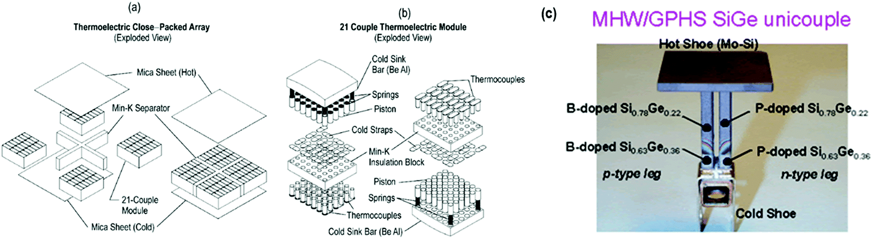 | ||
| Fig. 21 Detailed demonstration of (a) high density close-packed array (CPA) thermoelectric modules and (b) 21 Couple spring-loaded thermoelectric modules (c) segmented unicouple technology (image courtesy NASA). | ||
b. Automotive industry. Si–Ge rectifiers coalesce the efficacy of Schottky rectifiers having thermal constancy of fast recovery diodes, empowering scientists and engineers to augment their power outlines of 100–200 V for enhanced efficiency, as shown in Fig. 22. The devices target applications in automotive sector, communications infrastructure, and server markets. By proposing a comprehensive secured-operating area encountering no thermal runaway till 175 °C, the AEC-Q101 acquiescent Si–Ge rectifiers were found to be particularly suitable for high temperature applications.
 | ||
| Fig. 22 Si–Ge rectifiers in automobile sector (image courtesy Nexperia). | ||
Recently, Si–Ge proved to have ideal rectifier performance by automobile industries and designers of varied systems working at elevated temperatures for better efficiency.172
As Fig. 23(a and b) displays, novel gadgets exhibit improved thermal stability, widening the secure operating area – from 145 °C, the temperature where the thermal runaway initiates the Schottky rectifiers to greater than 175 °C for SiGe rectifiers, the stipulated threshold of the Clip-bonded Flat Power (CFP) package.
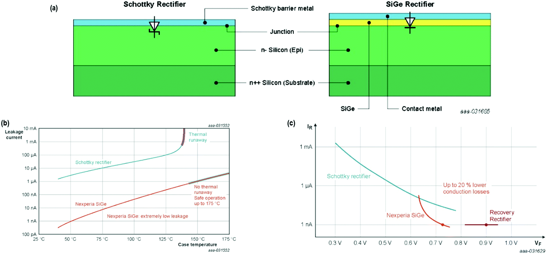 | ||
| Fig. 23 (a) Structural difference between a Schottky and SiGe rectifier; (b) plot of leakage current as a function of case temperature for a Schottky and a SiGe rectifier. When the leakage current turns out to be super-exponential, thermal runaway occurs; (c) compromise in forward voltage vs. leakage current for Schottky rectifier, Nexperia SiGe, and Fast Recovery rectifiers. The SiGe rectifier demonstrates approx. two orders of magnitude less leakage current in comparison to the Schottky rectifier, and approx. 20% reduced forward voltage drop in contrast to Fast Recovery rectifier. Adapted from ref. 173. | ||
Concerning the efficacy, Fig. 23(c) shows that usually a Fast Recovery rectifier exhibits approx. 0.9 V forward voltage. However, the Si–Ge diode presently shows the least leakage current (1 nA) of the family, where the curve is equated to a forward voltage (VF) of about 0.75 V and a gain of 150 mV. The outcome is a decrease in the losses due to conduction of nearby 20%. As an estimate, 5–10% enhanced efficiency could be envisioned, having analogous thermal stability in comparison to the finest-reported fast recovery diodes.173
c. Electronics and telecommunication industry. The Si–Ge heterojunction bipolar transistor (HBT), as shown in Fig. 24, happens to be the foremost realistic bandgap-engineered gadget to be accomplished in the silicon material system.155
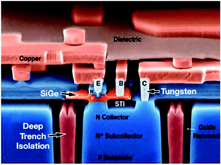 | ||
| Fig. 24 Schematic of Si–Ge heterojunction bipolar transistor for Bi-CMOS technology. Adapted from ref. 179b. | ||
Circuit designers and microelectronic device have long strived to unite the exceptional transport properties and design suppleness accessible by bandgap engineering (as normally performed in semiconductors, viz., GaAs and InP),174,175 with superior yield and low cost of conventional Si fabrication. The vision could finally be materialized by the introduction of epitaxial silicon germanium (Si–Ge) alloys.
The amalgamation of Si–Ge HBTs having the best-of-breed silicon CMOS to form a Si–Ge HBT BiCMOS demonstrates an obvious fit for delivering upcoming system-on-a-package and system-on-a-chip integrated circuit solutions.176–179
While the Si–Ge technology experiences a rising significance in performance-constrained digital, analog,180 and RF through mm-wave circuits and systems, budding Si–Ge applications for which reliability concerns exist both nuanced challenges and thrilling prospects include the quantum realm, power electronics, space systems, and integrated photonics.
Thus, a multinational company, MACOM,181 utilized its expertise in extremely high frequency (EHF), i.e., mmW circuit design and microwave, which joined in the Si–Ge commercialization endeavor throughout the 1990s with the fabrication and development of several monolithic microwave integrated circuit (MMIC) designs that attained extensive recognition in several handset and base station diligences.182 MACOM has also led the avenue in applying Si–Ge BiCMOS technology for both military and commercial demands.
Another, multinational industry Maxim integrated already illustrated that Si–Ge is capable of RF front-end performance.183 Moreover, due to low saturation voltage than silicon, Si–Ge seeks wide application in high-current devices. Moreover, better high-quality signal spectrum can be processed using the Si–Ge binary alloy.
A recent study by Fadaly et al. revealed, hexagonal Si–Ge alloy synthesized using the crystal transfer method with gallium phosphide (GaP) core nanowire having a wurtzite structure as a template, showing direct band gap, which is dissimilar to the traditional cubic lattice structure of the group-IV elements in the electronics industry (Fig. 25(a and b)). This leads to temperature-insensitive radiative recombination lifetime in sub-nanosecond, which causes light emission (an elusive for decades) comparable to group-III–V semiconductors having direct-bandgap. Thus, the light-emitting SiGe alloy opens a new avenue for a photonic chip, the latest revolution in integrated chip function.184,185
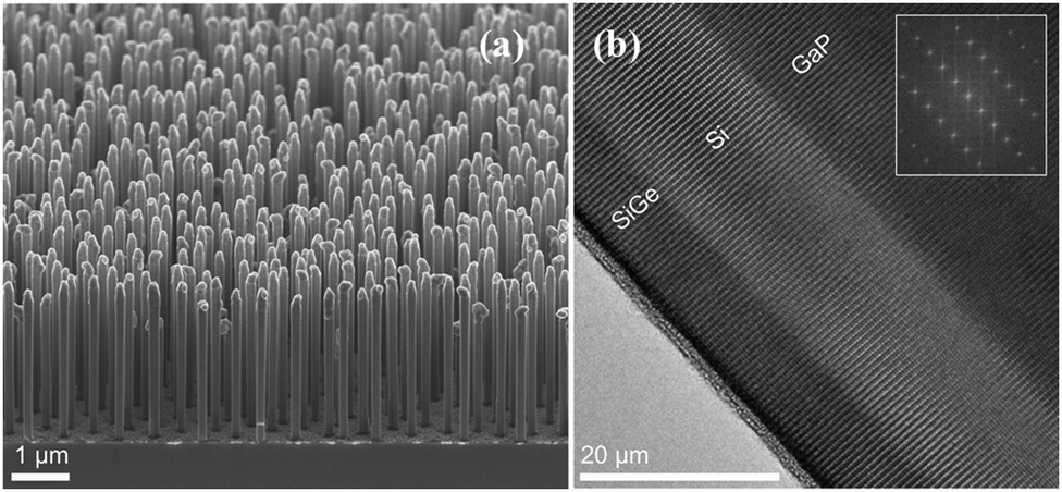 | ||
| Fig. 25 (a) SEM image of the GaP/Si/SiGe core/multishell NWs with hexagonal structure; (b) the HAADF HRSTEM image of the SiGe/Si/GaP interfaces and the corresponding FFT as the inset. Reproduced with permission from ref. 184. | ||
d. Solar Industry. Si–Ge possess both an elevated electron and hole mobility than Si, i.e., with less energy loss and 4× faster carrier mobility in comparison to single crystal silicon; it can be utilized for enhanced processing power, reduced dimension, and power fetching for a unit of similar size.
In photovoltaics (PV), Si–Ge is a favorable candidate to meet the outstanding need with enhanced adsorption characteristics and better conversion efficiency as the cell structures demand materials having bandgap similar to Ge but open-circuit voltage (VOC) similar to that of silicon. However, due to the losses in VOC and inadequacy in the crystal quality, SiGe lacks practical applications in PV cells.
Zhao et al. mentioned that the use of expensive traditional substrates in the III–V multi-junction devices regulates their application; in this regard, Si–Ge was chosen to be a promising material for bottom cell in a two-fold junction system owing for good process compatibility, excessive mobility, tunable lattice parameter, and competence to absorb light of wavelengths ∼1800 nm, which are supposed to be the most notable factors for bottom cell material selection in a two-terminal configuration (Fig. 26(a and b)).186
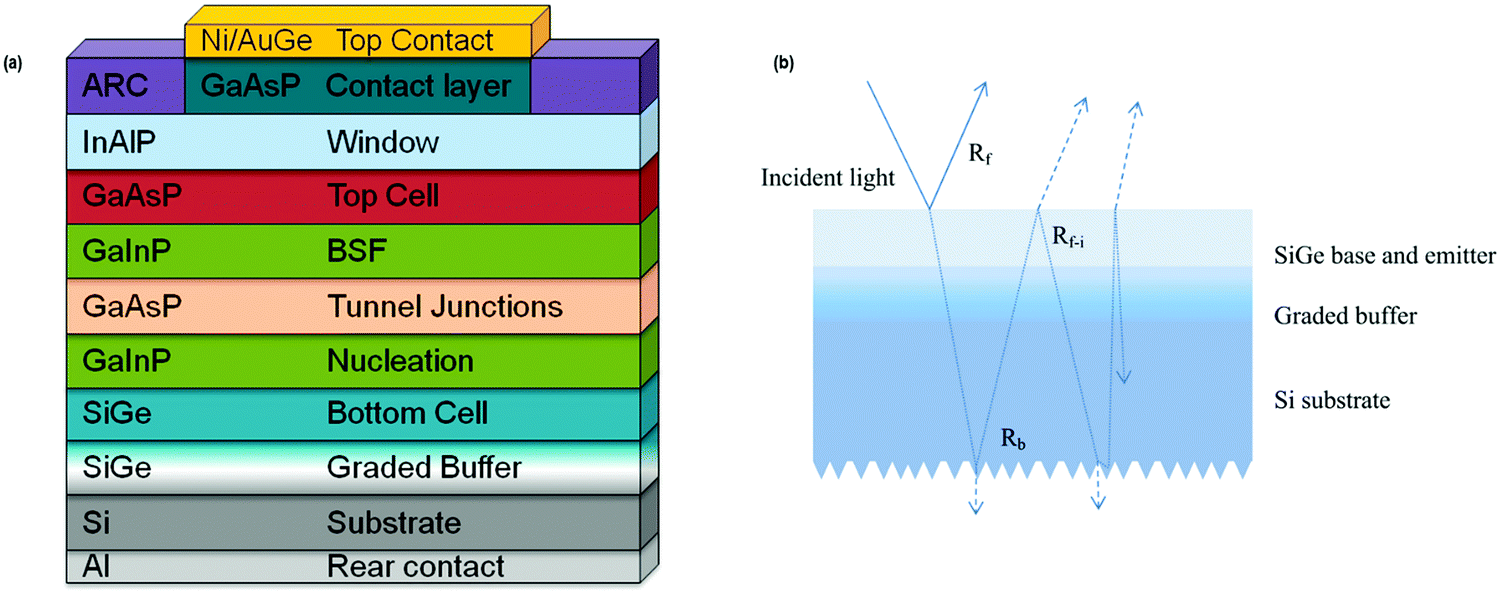 | ||
| Fig. 26 (a) Tandem device structure design of basic two-terminal GaAsP/SiGe on Si. Reproduced with permission from ref. 187; (b) optical paths in the Si–Ge structure. Reproduced with permission from ref. 186. | ||
Diaz et al. reported an efficacy of 18.9% under one sun from the GaAsP-SiGe structure, whereas Wang et al. reported that for the GaAsP-SiGe cell, an efficiency of over 20% can be achieved in the III–V epitaxial layers having a threading dislocation density (TDD).187
In other words, although Si and Ge are abundant elements in Earth's crust, they become expensive when synthesized in the laboratory as the process involves refining, followed by tedious single crystal or polycrystalline alloy formation. Fortunately, SiGe's growing acceptance has made it more available in the recent years, specifically in components geared for telecommunications, automotive, and solar environments.
2.5. Synergistic connection of the Si–Ge alloy in semiconductor and thermoelectric applications
In the Upcoming Industrial Revolution, the paradigm of Internet of Things (IoT) is likely to gain wide recognition owing to its vast applicability in a universal network. These IoT sensors are low energy wireless modules, typically driven by batteries, which are non-renewable energy storage units. However, these batteries pose constraints due to limited life-time; thus, frequent replacement is unviable. In this regard, the realization of miniaturized energy scavengers or energy harvester-controlled micro electro mechanical-system (MEMS) seems to be a solution to conjugate the prime requirement of IoT usage, viz., self-sufficiency in energy and integration or miniaturization.188–193 These energy harvesters are micro or nanoscale thermoelectric generators capable of supporting power requirement to IoT sensors in the range of few microwatts. Silicon and its Group-IV partner, which forms binary or ternary alloy, are promising to form μ-TEG as they are compatible with the traditional CMOS fabrication methodology and can be integrated at the chip level effortlessly. These also harmonize the need for economic and miniaturized systems.2.6. Conclusion
In conclusion, this review article has shown that with the prevailing COVID-19 crises, performing communication coordination for the extensive use of video conferences, home office, etc., retain paramount significance for maintaining the economy and stability under lockdown situations. In addition, the resilience concept is acquiring significance in the political domain and is presently resonating alongside the common public owing to the COVID-19 emergency. The country's strategic sectors, viz., the communication system, is a supreme issue, and understanding its importance is highly indispensable.Several projects such as Toward Advanced bicmos NanoTechnology platforms for radiofrequency (RF) and terahertz (thz) applicatiOns (TARANTO) in Europe aims at further strengthening the semiconductor industry in the Si–Ge BiCMOS technology and offering a concrete industrial base for the progress of novel products in areas such as home electronics, telecommunications, and car electronics that are of fundamental significance for high-tech industries. In fact, engineers and researchers worldwide are aimed for the setting up of subsequent BiCMOS technology programmes having enhanced performances of Si–Ge Higher Integration level and Heterojunction Bipolar Transistor (HBT) needed to tackle Enhanced Speed & Enhanced Data Rate communication systems. In fact, the enhanced execution of BiCMOS technology programmes are a major enabler of those functions that need the blend of front-ends high-performance radio-frequency (RF) along with advanced CMOS nodes having elevated computational power and low power consumption.194
Leibniz Institute for High-Performance Microelectronics (IHP) has studied numerous device concepts for Si–Ge HBTs pertaining to their ability to have enhanced performance in RadioFrequency.195 The speediest apparatus were attained in a practice having non-selective epitaxial growth (NSEG) of the Si–Ge base and elevated extrinsic base (EEB) regions made in a careful epitaxial process distinctly. In a bipolar-only procedure, the device concept is optimized following the illustration of ring oscillator gate delays of 1.34 ps and peak values of 505 GHz/720 GHz, which are descent values described for Si–Ge HBTs to date.196–198
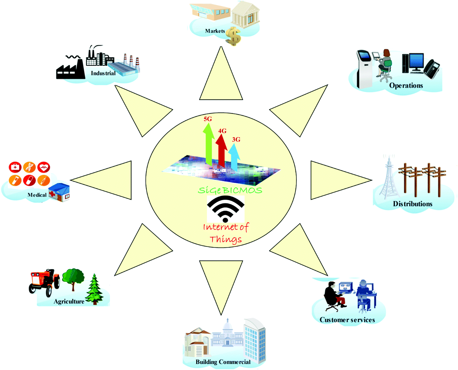
IHP in collaboration with X-FAB will work on advanced Si–Ge bipolar CMOS (BICMOS) technologies based on IHP's Si–Ge HBT's, which will be integrated on single circuit devices. Thus, Si–Ge BICMOS remains a lucrative prospect in several wireless applications such as 5G due to the amalgamation of enhanced performance radiofrequency on an Si-based substrate.199–201 Moreover, through the Internet of Things (IoT), Bipolar Junction Transistors empower Bi-CMOS toward supporting the nation's strategic and civilian welfares as it links the appliances and sensors to data acquisition system or computers and the internet for creating an intelligent system, hence making smart decisions and responding seamlessly. Fig. 27 illustrates the smart environment using IoT-based IV–IV binary alloy. In fact, the superior features of Si–Ge in comparison to Si lies on the fact that substituting some Si atoms with Ge deforms the crystal lattice and enhances the pace of the electrons to facilitate 1000× rapider systems. These expeditious systems have wide applicability in systems related to high-end communications.202–205
 | ||
| Fig. 27 IoT-based smart environment using the Si–Ge based BICMOS technology. | ||
Tower Semiconductor Ltd, a leading foundry of high-end analog semiconductor solutions from Israel, introduced a latest RF switch technology targeted at 5G (ranging from the sub-6 Hz bands and millimetre waves) smartphones and the cellular base stations that are capable of connecting them to ultrafast networks. The novelty of the switch technology is that Internet of Things devices can be used with limited battery life. The company claims to have the ability to integrate the RF switches with other production processes it offers customers, including SiGe BiCMOS and power CMOS. In this regard, several chips based on its SiGe, BiCMOS, RF CMOS, image sensor based on CMOS, assimilated power management, MEMS, as well as other production processes were introduced.206,207 Moreover, according to BIS research, which gives an overview of the place for market intelligence on deep technology, which includes research of more than 70 companies across the value chain, painstaking compilation of more than 700 research hours across 231 pages, and exclusive insight from in-depth expert interviews, forecasts that global silicon and germanium materials, is projected to grow to 5045.3 million dollars by 2021 on a compounded annual growth rate (CAGR) of 13.7 from 2016 to 2021. This technology is swelling into varied end-markets owing to communications devices, lightweight, automobile collision avoidance systems, and thermoelectric capabilities. Nevertheless, the rapid growth of internet, high mobile acceptance, and growth in the global self-governing driving industry are the key opportunities lined up in the Si–Ge market in the coming future.208,209
Moreover, Si–Ge seeks wide applicability in the energy harvesting sector as high temperature thermoelectric modules, especially in deep space planetary explorations. In this regard, initially, the space agencies synthesized single crystal Si–Ge alloy; subsequently, the work was extended to polycrystalline Si–Ge alloys as it is very much essential to understand the properties of the alloy extensively in a single crystal alloy. Nevertheless, the difficult synthetic procedures, to achieve single crystalline Si–Ge alloy with fixed compositions, were overcome by several groups worldwide using the various techniques, as discussed in the review.
Although, in recent years, polycrystalline Si–Ge has gained wide applicability in thermoelectric research, single crystalline Si–Ge alloy still enjoys widespread usage in the electronics and semiconductor industry.
Conflicts of interest
No conflict of interest.Acknowledgements
The author would like to acknowledge Dr Ajay Singh and Dr K. P. Muthe for valuable discussions for this article.References
- R. A. Smith, Semiconductors, 2nd edn, Cambridge University Press, London, 1979 Search PubMed.
- https://en.wikipedia.org/wiki/History_of_the_transistor .
- https://www.materialstoday.com/crystalline-materials/news/new-form-of-silicon-for-semiconductor-technology/ .
- E. Haller, Ge-based devices from materials to devices, Mater. Sci. Semicond. Process., 2006, 9(6), 408–422 CrossRef CAS.
- K. Prabhakaran and T. Ogino, Oxidation of Ge(100) and Ge(111) surfaces: An UPS and XPS study, Surf. Sci., 1995, 325(3), 263–271 CrossRef CAS.
- G. K. Teal, M. Sparks and E. Buehler, Growth of germanium single crystals containing p–n junctions, Phys. Rev., 1951, 81(4), 637 CrossRef CAS.
- https://www.materialstoday.com/crystalline-materials/news/novel-hexagonal-form-of-silicon/ .
- https://www.greatachievements.org/?id=3967 .
- N. N. Greenwood and A. Earnshaw, Chemistry of the Elements, 2nd edn, Butterworth-Heinemann, Oxford, 1997 Search PubMed.
- A. F. Holleman, E. Wiberg and N. Wiberg, Lehrbuch der Anorganischen Chemie, 102nd edn, de Gruyter, Berlin/New York, 2007 Search PubMed.
- D. I. Kaji Masanori, Mendeleev's concept of chemical elements and the principles of chemistry, Bull. History Chem., 2002, 27(1), 4–16 Search PubMed.
- https://www.nytimes.com/1953/05/10/archives/germanium-for-electronic-devices.html .
- https://www.ibm.com/ibm/history/ibm100/us/en/icons/siliconchip/ .
- D. L. Harame and B. S. Meyerson, The early history of IBM's SiGe mixed signal technology, IEEE Trans. Electron Devices, 2001, 48(11), 2555–2567 CrossRef.
- W. Barnett; P. Dick; B. Beaudry; P. Gorsuch and E. A. Skrabek, Thermoelectric Alloys and Devices for Radioisotope Space Power Systems: State of the Art and Current Developments, report, January 1, 1989; Washington D.C. (https://digital.library.unt.edu/ark:/67531/metadc843871/: accessed August 27, 2021), University of North Texas Libraries, UNT Digital Library, https://digital.library.unt.edu; crediting UNT Libraries Government Documents Department.
- R. Basu and A. Singh, High temperature Si–Ge alloy toward thermoelectric applications: A comprehensive review, Mater. Today Phys., 2021, 21, 100468 CrossRef CAS.
- https://www.cisco.com/c/en/us/solutions/collateral/executive-perspectives/annual-internet-report/white-paper-c11-741490.html .
- S. Wirths, D. Buca and S. Mantl, Si–Ge–Sn alloys: From growth to applications, Prog. Cryst. Growth Charact. Mater., 2016, 62(1), 1–39 CrossRef CAS.
- R. Szweda, C. Teddy O' and R. Marco, Experts see SiGe holding its own, III-Vs Review, 2004, 17(6), 32–35 CrossRef.
- https://www.ibm.com/blogs/research/2014/07/smaller-chip-with-bigger-bandwidth-thanks-to-e-band-and-sige/ .
- https://technology.nasa.gov/patent/LAR-TOPS-320 .
- D. Amaresh and D. Debajyoti, Optoelectronic and structural properties of Ge-rich narrow band gap nc-SixGe1−x absorber layer for tandem structure nc-Si solar cells, J. Phys. Chem. Solids, 2021, 154, 110055 CrossRef.
- S. Zhang, T. Zhang, Z. Liu, J. Wang, L. Yu, J. Xu, K. Chen and P. R.-I. Cabarrocas, Highly flexible radial tandem junction thin film solar cells with excellent power-to-weight ratio, Nano Energy, 2021, 86, 106121 CrossRef CAS.
- C. Pablo, H. Manuel, N. Huy, M. Aled, M. D. Fuertes, G. Iván, J. Andrew and R.-S. Ignacio, Hybrid III-V/SiGe solar cells grown on Si substrates through reverse graded buffers, Sol. Energy Mater. Sol. Cells, 2020, 205, 110246 CrossRef.
- A. Maurizio, I. Subramanian, M. Bernard, P. Gary and S. Johannes, Si single bond Ge alloys: Growth, properties and applications, Appl. Surf. Sci., 1991, 48–49, 377–386 Search PubMed.
- In Silicon, Germanium, and Their Alloys: Growth, Defects, Impurities, and Nanocrystals (1st ed.), ed. G. Kissinger and S. Pizzini, CRC Press, 2014 DOI:10.1201/b17868.
- D. M. Rowe, CRC handbook of thermoelectrics, CRC, Boca Raton, FL, 1995 Search PubMed.
- R. W. Olesinski and G. J. Abbaschian, The Ge–Si (germanium–silicon) system, Bull. Alloy Phase Diagrams, 1984, 5(2), 180–183 CrossRef CAS.
- N. Usami, Types of silicon–germanium (SiGe) bulk crystal growth methods and their applications Silicon–germanium (SiGe) Nanostructures Production, Properties and Applications in Electronics Woodhead Publishing Series in Electronic and Optical Materials, 2011, pp. 72–82 Search PubMed.
- L. Rittenhouse Tilghman, Single Crystal Growth and Characterization of Silicon Germanium Alloys MS thesis, http://file:///tmp/42713448-MIT.pdf.
- K. Seevakan and S. Bharanidharan, Different types of crystal growth methods, Int. J. Pure Appl. Math., 2018, 119(12), 5743–5758 Search PubMed.
- H. Jürg, Chemistry and crystal growth, Angew. Chem., Int. Ed. Engl., 1994, 33(2), 143–162 CrossRef.
- N. Tatau, Handbook of Crystal Growth, Fundamentals: Thermodynamics and Kinetics, 2nd edn, vol. IA, 2015 Search PubMed.
- N. Tatau, Handbook of Crystal Growth, Fundamentals: Transport and Stability, 2nd edn, vol. IB, 2015 Search PubMed.
- M. G. John, Y. Nima, P. Chris, J. H.-ter Horst and S. Jan, Chapter 1: Nucleation and Crystal Growth in Continuous Crystallization, in The Handbook of Continuous Crystallization, 2020, pp. 1–50 10.1039/9781788013581-00001 eISBN: 978-1-78801-358-1.
- A. F. May, J. Yan and M. A.-J. McGuire, A practical guide for crystal growth of van der Waals layered materials, Appl. Phys., 2020, 128(5), 051101 CAS.
- M. Tachibana, Beginner's Guide to Flux Crystal Growth, Springer, 2017 Search PubMed.
- M. Muehlberg, in Crystal Growth Technology: From Fundamentals and Simulation to Large scale Production, ed. H. J. Scheel and P. Capper, Wiley-VCH Verlag GmbH & Co. KGaA, Weinheim, 2008, ch. 1, pp. 2–26 Search PubMed.
- M. G. Kanatzidis, R. Pöttgen and W. Jeitschko, The metal flux: A preparative tool for the exploration of intermetallic compounds, Angew. Chem., Int. Ed., 2005, 44(43), 6996–7023 CrossRef CAS PubMed.
- J. F. Shackelford, Introduction to Materials Science for Engineers, Prentice Hall, 1999 Search PubMed.
- A. R. West, Basic Solid State Chemistry, John Wiley & Sons Incorporated, 1999 Search PubMed.
- I. R. Fisher, M. C. Shapiro and J. G. Analytis, Principles of crystal growth of intermetallic and oxide compounds from molten solutions, Philos. Mag., 2012, 92(19–21), 2401–2435 CrossRef CAS.
- J. Venkrbec, Phase diagrams and crystal growth, J. Cryst. Growth., 1980, 48(4), 611–620 CrossRef CAS.
- J. Scheel Hans, Historical aspects of crystal growth technology, J. Cryst. Growth, 2000, 211(1), 1–12 CrossRef.
- https://commons.wikimedia.org/wiki/File%3ASingle_Crystal_Growth_Methods_Tree_Diagram_.png .
- R. Fornari, Electronic materials and crystal growth Single Crystals of Electronic Materials Growth and Properties Woodhead Publishing Series in Electronic and Optical Materials, 2019, pp. 1–3 Search PubMed.
- https://www.sciencedirect.com/topics/chemistry/bridgman-technique .
- D. Nicoara and I. Nicoara, An improved Bridgman-Stockbarger crystal-growth system materials, Mater. Sci. Eng., A, 1988, 102(2), L1–L4 CrossRef.
- A. Barz, P. Dold, U. Kerat, S. Recha, K. W. Benz, M. Franz and K. Pressel, Germanium-rich SiGe bulk single crystals grown by the vertical Bridgman method and by zone melting, J. Vac. Sci. Technol., B, 1998, 16(3), 1627–1630 CrossRef CAS.
- A. Dario, H. O. Sicim and E. Balikci, A comparative study on the growth of germanium–silicon single crystals grown by the vertical Bridgman and axial heat processing techniques, J. Cryst. Growth, 2012, 351(1), 1–8 CrossRef CAS.
- A. Dahlen, A. Fattahg, G. Hanke and E. Karthaus, Bridgman and Czochralski growth of Ge–Si alloy crystals, Cryst. Res. Technol., 1994, 29(2), 187–198 CrossRef CAS.
- J. Czochralski, Ein neues Verfahren zur Mes-sung des Kristallisationsgeschwindigkeit der Metalle, Z. Phys. Chem., 1918, 92U(1), 219–221 CrossRef.
- I. Yonenaga, Growth and fundamental properties of SiGe bulk crystals, J. Cryst. Growth, 2005, 275(1), 91–98 CrossRef CAS.
- J. Friedrich, L. Stockmeier and G. Müller, Constitutional supercooling in czochralski growth of heavily doped silicon crystals, Acta Phys. Pol., A, 2013, 124(2), 219–226 CrossRef CAS.
- M. Kürten and J. Schilz, Czochralski growth of SixGe1−x single-crystals, J. Cryst. Growth, 1994, 139(1–2), 1–5 CrossRef.
- R. H. Deitch, S. H. Jones and T. G. Digges, Bulk single crystal growth of silicon–germanium, J. Electron. Mater., 2000, 29(9), 1074–1078 CrossRef CAS.
- N. V. Abrosimov, S. N. Rossolenko, W. Thieme, A. Gerhardt and W. Schröder, Czochralski growth of Si- and Ge-rich SiGe single crystals, J. Cryst. Growth, 1997, 174(1-2), 182–186 CrossRef CAS.
- N. Usami, Chapter-4: Types of silicon–germanium (SiGe) bulk crystal growth methods and their applications, in Silicon–Germanium (SiGe) Nanostructures: Production, Properties and Applications in Electronics, ed. Shiraki, Y. and Usami, N., Woodhead Publishing Limited, Sawston, UK, 2011, pp. 72–82 Search PubMed.
- W. A. Tiller, K. A. Jackson, J. W. Rutter and B. Chalmers, The Redistribution of solute atoms during the solidification of metals, Acta Metall., 1953, 1(4), 428–437 CrossRef CAS.
- W. G. Pfann, Zone Melting, Wiley, New York, 2nd edn, 1964 Search PubMed.
- W. G. Pfann, Principles of zone-melting, Trans. AIME, 1952, 194, 747 Search PubMed.
- P. Kapitza, The study of the specific resistance of bismuth crystals and its change in strong magnetic fields and some allied problems, Proc. R. Soc. A, 1928, 119(782), 358–443 CAS.
- E. N.-da C. Andrade and R. Roscoe, Glide in metal single crystals, Proc. Phys. Soc., 1937, 49(2), 152–177 CrossRef CAS.
- J. C. Fan, M. W. Geis and B. Y. Tsaur, Lateral epitaxy by seeded solidification for growth of single-crystal Si films on insulators, App. Phys. Lett., 1981, 38(5), 365–367 CrossRef CAS.
- I. N. Miaouli, P. Y. Wong, S. M. Yoon, R. D. Robinson and C. K. Hess, Thermal analysis of zone-melting recrystallization of silicon-on-insulator structures with an infrared heat source: An overview, J. Electrochem. Soc., 1992, 139(9), 2687–2696 CrossRef.
- K. Kubota, C. E. Hunt and J. Frey, Thermal profiles during recrystallization of silicon on insulator with scanning incoherent light line sources, Appl. Phys. Lett., 1985, 46(12), 1153–1155 CrossRef CAS.
- H. H. Richer and B. Tillack, Thermal analysis on zone-melting recrystallization of silicon-on-insulator films using a finite difference method, Mater. Sci. Eng., A, 1993, 173(1-2), 59–62 CrossRef.
- L. Yu, X. Kang, L. Chen, K. Luo, Y. Jiang and X. Cao, Research status of high-purity metals prepared by zone refining, Materials, 2021, 14, 2064 CrossRef CAS PubMed.
- A. B.-I. Bollong, R. P. Bult and G. T. Proux, Method for the zone refining of gallium, US Pat., 4888051, 1989 Search PubMed.
- J. H. Beynon and R. A. Saunders, Purification of organic materials by zone refining, Br. J. Appl. Phys., 1960, 11(3), 128–131 CrossRef CAS.
- K. Ghosh, V. N. Mani and S. Dhar, A modeling approach for the purification of group III metals (Ga and In) by zone refining, J. Appl. Phys., 2008, 104(2), 024904 CrossRef.
- H. Wan, B. Xu and B. Yang, et al., Effect of silicon separation on the preparation of high-purity aluminum, Silicon, 2021, 13, 399–407 CrossRef CAS.
- M. F. McNamara, J. A. Slattery and A. F. Witt, Process for ultra-purification of indium, US Pat., 4828608, 1989 Search PubMed.
- R. P. Bult, A. B.-I. Bollong and R. F. Redden, Purification of Cd and Te by zone refining, US Pat., 4690725, 1987 Search PubMed.
- A. Burger, D. O. Henderson, S. H. Morgan, J. Feng and E. Silberman, Purification of selenium by zone refining, J. Cryst. Growth, 1990, 106(1), 34–37 CrossRef CAS.
- G. Zha, Y. Wang, M. Cheng, D. Huang, W. Jiang, B. Xu and B. Yang, Purification of crude selenium by vacuum distillation and analysis, J. Mater. Res. and Tech., 2020, 9(3), 2926–2933 CrossRef CAS.
- S. S. Cohen, P. W. Wyatt, G. H. Chapman and J. M. Canter, Laser-induced diode linking for wafer-scale integration, IEEE Trans. Electron. Dev., 1988, 35(9), 1533–1550 CrossRef.
- G. W. Young and A. Chait, Steady-state thermal-solutal diffusion in a float zone, J. Cryst. Growth, 1989, 96(1), 65–95 CrossRef.
- N. Cheung, R. Bertazzoli and A. Garcia, Experimental impurity segregation and numerical analysis based on variable solute distribution coefficients during multi-pass zone refining of aluminum, J. Cryst. Growth, 2008, 310(6), 1274–1280 CrossRef CAS.
- T. Ikeda, N. J. Marolf and G. J. Snyder, Zone leveling crystal growth of thermoelectric PbTe alloys with Sb2Te3 Widmanstätten precipitates, Cryst. Growth Des., 2011, 11(9), 4183–4189 CrossRef CAS.
- P. Rudolph, Handbook of Crystal Growth, Handbook of Crystal Growth (Second Edition), Elsevier, 2015, p. iii, ISBN 9780444633033 Search PubMed.
- J. K. Kennedy, Continuous zone-refining apparatus, Rev. Sci. Instrum., 1964, 35(1), 25–28 CrossRef CAS.
- D. R. Mason and J. S. Cook, Zone leveling and crystal growth of peritectic compounds, J. Appl. Phys., 1961, 32(3), 475477 CrossRef.
- J. A. Burton, R. C. Prim and W. P. Slichter, The distribution of solute in crystals grown from the melt. Part I. theoretical, J. Chem. Phys., 1953, 21(11), 1987 CrossRef CAS.
- J. A. Burton, E. D. Kolb, W. P. Slichter and J. D. Struthers, Part II. Experimental, J. Chem. Phys., 1953, 21(11), 1991 CrossRef CAS.
- A. Borshchevsky, Preparation of Thermoelectric Materials from Melts, CRC Press, Florida, USA, 1995, vol. 1, p. 90 Search PubMed.
- M. S. Saidov, A. Yusupov and R. S. Umerov, Si–Ge solid-solution single- crystal growth by electron-beam floating zone technique, J. Cryst. Growth, 1981, 52, 514–518 CrossRef CAS.
- G. F. Bolling and W. A. Tiller, Growth from the melt. Part II. Cellular interface morphology, J. Appl. Phys., 1960, 31(11), 2040–2045 CrossRef CAS.
- J. Wollweber, D. Schulz and W. SchriSder, Extremely reduced dislocation density in SixGel−x single crystals grown by the float zone technique, J. Cryst. Growth, 1996, 1(58), 166–168 CrossRef.
- J. Wollweber, D. Schulz and W. Schröder, SixGe1−x single crystals grown by the RF-heated float zone technique, J. Cryst. Growth, 1996, 163(3), 243–248 CrossRef CAS.
- T. A. Campbell, M. Schweizer, P. Dold, A. Croll and K. W. Benz, Float zone growth and characterization of Ge1−xSix (x ≤ 10 at%) single crystals, J. Cryst. Growth, 2001, 226(2), 231–239 CrossRef CAS.
- E. M. Swiggard, Liquid encapsulated zone melting crystal growth method and apparatus, US Pat., 5007980, 1991 Search PubMed.
- D. Bliss, B. Demczyk, A. Anselmo and J. Bailey, Silicon–germanium bulk alloy growth by liquid encapsulated zone melting, J. Cryst. Growth, 1997, 174(1–4), 187–193 CrossRef CAS.
- J. Bailey, B. G. Demczyk and D. F. Bliss, Silicon–germanium bulk alloy growth by liquid encapsulated zone melting, US Pat., 6143070, 2000 Search PubMed.
- N. Kazuo, K. Toshihiro, A. Yukinaga, U. Noritaka, F. Kozo, U. Toru, S. Gen and S. Toetsu, Compositional variation in Si-rich SiGe single crystals grown by multi-component zone melting method using Si seed and source crystals, J. Cryst. Growth, 2002, 240(3-4), 373–381 CrossRef.
- T. Suzuki, K. Nakajima, T. Kusunoki and T. Katoh, Multicomponent zone melting growth of ternary InGaAs bulk crystal, J. Electron. Mater., 1996, 25, 357–361 CrossRef CAS.
- K. Nakajima, T. Kusunoki and K. Otsubo, Bridgman growth of compositionally graded InxGa1−xAs (x = 0.05–0.30) single crystals for use as seeds for In0.25Ga0.75As crystal growth, J. Cryst. Growth, 1997, 173(1–2), 42–50 CrossRef CAS.
- K. Nakajima, S. Kodama, S. Miyashita, G. Sazaki and S. Hiyamizu, Growth of Ge-rich SixGe1−x single crystal with uniform composition (x = 0.02) on a compositionally graded crystal for use as GaAs solar cells, J. Cryst. Growth, 1999, 205(3), 270–276 CrossRef CAS.
- Y. Azuma, N. Usami, T. Ujihara, G. Sazaki, Y. Murakami, S. Miyashita, K. Fujiwara and K. Nakajima, Growth of SiGe bulk crystal with uniform composition by directly controlling the growth temperature at the crystal-melt interface using in situ monitoring system, J. Cryst. Growth, 2001, 224(3–4), 204–211 CrossRef CAS.
- I. Yonenaga, Segregation during the seeding process in the Czochralski growth of GeSi alloys, J. Cryst. Growth, 1998, 191(3), 399–404 CrossRef CAS.
- A. Borshchevsky and J. P. Fleurial, Growth of heavily doped Si–Ge from metallic solutions, J. Cryst. Growth, 1993, 128(1-4), 331–337 CrossRef CAS.
- (a) J. H. Peterson, M. Fiederle and J. J. Derby, Analysis of the traveling heater method for the growth of cadmium telluride, J. Cryst. Growth, 2016, 454(15), 45–58 CrossRef CAS; (b) T. Robert, Crystal Growth by Traveling Heater Method, Handbook of Crystal Growth, Elsevier, 2nd edn, 2015, pp. 459–504 Search PubMed.
- D. Labrie, A. E. George, M. Jamieson, S. Obruchkov, J. P. Healey and B. E. Paton, Single crystal growth of Ge1−xSix alloys using the traveling solvent method, J. Vac. Sci. Technol. A, 2004, 22, 962 CrossRef CAS.
- I. Kostylev, J. K. Woodacre, Y. P. Lee, P. Klages and D. Labrie, Melt zone growth of Ge-rich Ge1−xSix bulk crystals, J. Cryst. Growth, 2013, 377(7), 147–152 CrossRef CAS.
- K. Abe, S. Sumioka, K.-I. Sugioka, M. Kubo, T. Tsukada, K. Kinoshita, Y. Arai and Y. Inatomi, Numerical simulations of SiGe crystal growth by the traveling liquidus-zone method in a microgravity environment, J. Cryst. Growth, 2014, 402, 71–77 CrossRef CAS.
- G. B. Stringfellow, Fundamentals of thin film growth, J. Cryst. Growth, 1994, 137(1-2), 212–223 CrossRef CAS.
- I. HoKim, Bi,Sb)2(Te,Se)3-Based thin film thermoelectric generators, Mater. Lett., 2000, 43(5), 221–224 Search PubMed.
- R. Venkatasubramanian, E. Siivola and T. Colpitts, et al., Thin-film thermoelectric devices with high room temperature figures of merit, Nature, 2001, 413, 597–602 CrossRef CAS PubMed.
- H. Böttner, G. Chen and R. Venkatasubramanian, Aspects of thin-film superlattice thermoelectric materials, devices, and applications, MRS Bull., 2006, 31(3), 211–217 CrossRef.
- B. Hinterleitner, I. Knapp, M. Poneder, Y. Shi, H. Müller and G. Eguchi, et al., Thermoelectric performance of a metastable thin-film Heusler alloy, Nature, 2019, 576, 85–90 CrossRef CAS PubMed.
- X. Chen, Z. Zhou, Y. H. Lin and C. Nan, Thermoelectric thin films: Promising strategies and related mechanism on boosting energy conversion performance, J. Materiomics, 2020, 6(3), 494–512 CrossRef.
- M. F. Silva, J. F. Ribeiro, J. P. Carmo, L. M. Gonçalves and J. H. Correia, Thin films for thermoelectric applications, in Scanning Probe Microscopy in Nanoscience and Nanotechnology 3, ed. Bhushan B., NanoScience and Technology, Springer, Berlin, Heidelberg, 2012 DOI:10.1007/978-3-642-25414-7_17.
- H. Nelson, Epitaxial growth from the liquid state and its application to the fabrication of tunnel and laser diodes, RCA Rev., 1963, 24, 603 Search PubMed.
- H. W. Li and C. W. Chang, Pressure-sensitive liquid phase epitaxy of highly doped n-type SiGe crystals for thermoelectric applications, Sci. Rep., 2019, 9, 4362 CrossRef PubMed.
- C. Littlejohns, M. Nedeljkovic and C. Mallinson, et al., Next generation device grade silicon–germanium on insulator, Sci. Rep., 2015, 5, 8288 CrossRef CAS PubMed.
- J. Wang, C. Heidelberger, A. Fitzgerald Eugene and J. Quitorianom Nathaniel, Liquid phase epitaxy SiGe films on a CVD-grown SiGe/Si(001) graded film, J. Cryst. Growth, 2020, 535(1), 125541 CrossRef CAS.
- W. X. Ni, G. V. Hansson, I. A. Buyanova, A. Henry, W. M. Chen and B. Momemar, Influence of ion bombardment on Si and SiGe films during molecular beam epitaxy growth, Appl. Phys. Lett., 1996, 68(2), 238–240 CrossRef CAS.
- M. Bauer, M. Oehme, K. Lyutovich and E. Kasper, Ion assisted MBE growth of SiGe nanostructures, Thin Solid Films, 1998, 336(1-2), 104–108 CrossRef CAS.
- M. Oehme, J. Werner, O. Kirfel and E. Kasper, MBE growth of SiGe with high Ge content for optical applications, Appl. Surf. Sci., 2008, 254(19), 6238–6241 CrossRef CAS.
- A. Y. Cho and J. R. Arthur, Molecular beam epitaxy. Progress in Solid-State, Chemistry, 1975, 10(3), 157–191 Search PubMed.
- J. R. Arthur, Molecular beam epitaxy, Surf. Sci., 2002, 500(1-3), 189–217 CrossRef CAS.
-
M. A. Herman and H. Sitter, Molecular Beam Epitaxy, Springer-Verlag, Berlin, 1st edn, 1988 Search PubMed.
- O. Aktas, Y. Yamamoto and M. Kaynak, et al., Non-isothermal phase-field simulations of laser-written in-plane SiGe heterostructures for photonic applications, Commun. Phys., 2021, 4(132), 1–12 Search PubMed.
- A. Y. Cho, Growth of III–V semiconductors by molecular beam epitaxy and their properties, Thin Solid Films, 1983, 100(4), 291–317 CrossRef CAS.
- O. Yusuke, Silicon molecular beam epitaxy with simultaneous ion implant doping, J. Appl. Phys., 1980, 51(2), 1102–1110 CrossRef.
- J. C. Bean and E. A. Sadowski, Silicon MBE apparatus for uniform high-rate deposition on standard format wafers, J. Vac. Sci. Technol., 1982, 20(2), 137 CrossRef CAS.
- H. Kibbel, E. Kasper, P. Narozny and H. U. Schreiber, Boron doping of Si–Ge base of heterobipolar transistors, Thin Solid Films, 1990, 184(1-2), 163–170 CrossRef CAS.
- Silicon Molecular Beam Epitaxy, ed. E. Kasper and J. C. Bean, CRC Press, Boca Raton, FL, 1988 Search PubMed.
- L. D. Hicks and M. S. Dresselhaus, Effect of quantum-well structures on the thermoelectric figure of merit, Phys. Rev. B, 1993, 47(19), 12727–12731 CrossRef CAS PubMed.
- T. Koga, X. Sun, S. B. Cronin and M. S. Dresselhaus, Carrier pocket engineering to design superior thermoelectric materials using GaAs/AlAs superlattices, Appl. Phys. Lett., 1998, 73(20), 2950–2952 CrossRef CAS.
- P. Pichanusakorn and P. Bandaru, Nanostructured thermoelectrics, Mater. Sci. Eng. R Rep., 2010, 67(2–4), 19–63 CrossRef.
- K.-N. Tu, J. W. Mayer and L. C. Feldman, Electronic thin film science: for electrical engineers and materials scientists, Maxwell Macmillan International, New York, 1992 Search PubMed.
- S. S. Iyer, M. Arienzo and E.-de Frésart, Low-temperature silicon cleaning via hydrogen passivation and conditions for epitaxy, Appl. Phys. Lett., 1990, 57(9), 893–895 CrossRef CAS.
- B. Berghaus, Improvements in and Related to the Coating of Articles by Means of Thermally Vapourized Material, UK Pat., 510992, 1938 Search PubMed.
- C. F. Powell; J. H. Oxley and J. M. Blocher, Vapour Deposition, John Wiley & Sons, New York, NY, USA, 1966 Search PubMed.
- D. M. Mattox, Handbook of Physical Vapor Deposition (PVD) Processing Film Formation, Adhesion, Surface Preparation and Contamination Control, Knovel, Norwich, NY, USA, 1998 Search PubMed.
- A. Baptista, F. Silva, J. Porteiro, J. Míguez and G. Pinto, Sputtering physical vapour deposition (PVD) coatings: A critical review on process improvement and market trend demands, Coatings, 2018, 8(11), 402–423 CrossRef.
- G. K. Teal, J. R. Fisher and A. W. Treptow, A new bridge photo-cell employing a photo-conductive effect in silicon. Some properties of high purity silicon, J. Appl. Phys., 1946, 17(11), 879–886 CrossRef CAS.
- J. C. Knights, Substitutional doping in amorphous silicon, Am. Inst. Phys. Conf., 1976, 31, 296–300 CAS.
- D. E. Carlson and C. R. Wronski, Amorphous silicon solar cell, Appl. Phys. Lett., 1976, 28(11), 671–673 CrossRef CAS.
- H. M. Manasevit, Recollections and reflections of MO-CVD, J. Cryst. Growth, 1981, 55, 1–9 CrossRef CAS.
- W. T. Tsang, Chemical beam epitaxy of InP and GaAs, Appl. Phys. Lett., 1984, 45(11), 1234–1236 CrossRef CAS.
- L. Sun, G. Yuan and L. Gao, et al., Chemical vapour deposition, Nat. Rev. Methods Primers, 2021, 1(5), 1–20 Search PubMed.
- H. Kühne, T. Morgenstern, P. Zaumseil, D. Krüger, E. Bugiel and G. Ritter, Chemical vapour deposition of epitaxial SiGe thin films from SiH4–GeH4–HCl–H2 gas mixtures in an atmospheric pressure process, Thin Solid Films, 1992, 222(1–2), 34–37 CrossRef.
- S. N.-R. Kazmi, A. Y. Kovalgin, A. A.-I. Aarnink, C. Salm and J. Schmitz, Low-stress highly-conductive in-situ boron doped Ge0.7Si0.3Films by CVD, ECS J. Solid State Sci. Technol., 2012, 1(5), 222–226 CrossRef.
- S. Kannan, C. Taylor and D. Allred, PECVD growth of Six:Ge1−x films for high speed devices and MEMS, J. Non-Cryst. Solids, 2006, 352(9–20), 1272–1274 CrossRef CAS.
- D. Dutartre, N. Loubet, F. Brossard, B. Vandelle, P. Chevalier, A. Chantre, S. Monfray, C. Fenouillet-Beranger, A. Pouydebasque and T. Skotnicki, Si/SiGe epitaxy: A ubiquitous process for advanced electronics, IEEE Int. Electron Devices Meet., 2007, 689–692, DOI:10.1109/IEDM.2007.4419039.
- J. M. Hartmann, et al. , Semicond. Sci. Technol., 2003, 19(3), 311–318 CrossRef.
- S. A. Shahahmadi, B. Yeganeh, N. Huda, N. Asim, M. Hafidz, M. M. Alam, Z. A. Alothman, K. Sopian and N. Amin, Properties of a-SiGe thin films on glass by co-sputtering for photovoltaic absorber application, J. Nanosci. Nanotechnol., 2015, 15(11), 9275–9280 CrossRef CAS PubMed.
- S. A. Shahahmadi, A. A. Zulkefle, A. K.-M. Hasan, S. M. Rana, B. Bais, M. Akhtaruzzaman, A. R.-M. Alamoud and N. Amin, Ge-rich SiGe thin film deposition by co-sputtering in in situ and ex-situ solid phase crystallization for photovoltaic applications, Mater. Sci. Semicond. Process., 2016, 56, 160–165 CrossRef CAS.
- W. K. Choi, L. K. Teh, L. K. Bera, W. K. Chim, A. T.-S. Wee and Y. X. Jie, Microstructural characterization of RF sputtered polycrystalline silicon germanium films, J. Appl. Phys., 2002, 91(1), 444–450 CrossRef CAS.
- K. Sasaki, K. Nakata and T. Hata, Epitaxial growth of SiGe thin films by ion-beam sputtering, Appl. Surf. Sci., 1997, 113–114, 43–47 CrossRef.
- K. Sasaki, Y. Nabetani, H. Miyashita and T. Hata, Heteroepitaxial growth of SiGe films and heavy B doping by ion-beam sputtering, Thin Solid Films, 2000, 369(1-2), 171–174 CrossRef CAS.
- J. Böck, H. Schäfer, H. Knapp, D. Zöschg, K. Aufinger, M. Wurzer, et al., High-speed SiGe:C bipolar technology, Tech. Dig. IEEE Int. Electron Devices Meeting, 2001, pp. 344–347.
- J. D. Cressler and G. Niu, Silicon–Germanium Heterojunction Bipolar Transistors, Artech House, MA, Boston, 2003 Search PubMed.
- J. D. Cressler, On the potential of SiGe HBTs for extreme environment electronics, Proc. IEEE, 2005, 93(9), 1559–1582 CAS.
- In Silicon Heterostructure Handbook: Materials, Fabrication, Devices, Circuits and Applications of SiGe and Si Strained-Layer Epitaxy (1st ed.), ed. J. D. Cressler, CRC Press, 2005 DOI:10.1201/9781315221137.
- A. Grebennikov, B. Sogl, H. Herrmann, C. Roth and W. Thomann, High-efficiency balanced switched-path monolithic SiGe HBT power amplifiers for wireless applications, in European Microwave Integrated Circuit Conference, 2007, pp. 391–394 Search PubMed.
- J. D. Cressler, SiGe BiCMOS Technology: An IC Design Platform for Extreme Environment Electronics Applications, in IEEE International Reliability Physics Symposium Proceedings, 2007, pp. 141–149 Search PubMed.
- P. V. Testa, V. Riess, C. Carta and F. Ellinger, A 130 nm-SiGe-BiCMOS low-power receiver based on distributed amplifier techniques for broadband applications from 140 GHz to 200 GHz, IEEE Open J. Circ. Syst., 2021, 2, 508–519 Search PubMed.
- T. Maiwald, K. Kolb, J. Potschka, M. Dietz and R. Weigel, Toward Broadband D-Band Wireless Communication Systems using Beam Steering in SiGe BiCMOS Technology, in 13th Global Symposium on Millimeter-Waves & Terahertz (GSMM), 2021, pp. 1–3 Search PubMed.
- E. Preisler, A Commercial Foundry Perspective of SiGe BiCMOS Process Technologies, in IEEE BiCMOS and Compound Semiconductor Integrated Circuits and Technology Symposium (BCICTS), 2020, pp. 1–5 Search PubMed.
- T. Suligoj, J. Žilak, Ž. Osrečki and M. Koričić, Versatile BiCMOS Technology Platform for the Low-cost Integration of Multi-purpose Applications, in IEEE Latin America Electron Devices Conference (LAEDC), 2021, pp. 1–4 Search PubMed.
- F. Baig, D. Bierbüsse, S. Chalermwisutkul and R. Negra, Active V-band Frequency Multiplier-by-4 Chain in SiGe HBT technology, in IEEE Asia-Pacific Microwave Conference (APMC), 2020, pp. 110–112 Search PubMed.
- W. Teng Jeffrey, Thesis on Design of RF receiver components for space applications using SiGe BICMOS, https://hdl.handle.net/1853/65129.
- https://digital.library.unt.edu/ark:/67531/metadc843871/m1/ .
- https://www.osti.gov/servlets/purl/4716190/ .
- C. Robin, S. Rochette, S. Desgrez, J. L. Muraro, D. Langrez, J. L. Roux and M. Krstic, Reliability evaluation of a 0.25μm SiGe technology for space applications, Microelectron. Reliab., 2019, 100–101, 113480 CrossRef CAS.
- S. Giannakopoulos, I. Sourikopoulos, L. Stampoulidis, P. Ostrovskyy, F. Teply, K. Tittelbach-Helmrich, G. Panic, G. Fischer, A. Grabowski, H. Zirath, P. Ayzac, N. Venet, A. Maho, M. Sotom, S. Jones, G. Wood and I. Oxtoby, A 112 Gb/s radiation-hardened mid-board optical transceiver in 130-nm SiGe BiCMOS for intra-satellite links, Front. Phys., 2021, 9, 252 Search PubMed.
- R. Basu and A. Singh, High temperature Si–Ge alloy toward thermoelectric applications: A comprehensive review, Mater. Today Phys., 2021, 21, 100468 CrossRef CAS.
- J. P. Fleurial, et al., Development of segmented thermoelectric multicouple converter technology, in IEEE Aerospace Conference, 2006, p. 10 Search PubMed.
- https://efficiencywins.nexperia.com/innovation/SiGe-rectifiers-thermally-stable-efficiency.html .
- https://www.powerelectronicsnews.com/cutting-edge-sige-rectifiers-enhancing-safe-operating-area-for-high-temperature-high-frequency-applications-2/ .
- P. Ashburn, SiGe Heterojunction Bipolar Transistors, John Wiley & Sons, Ltd, 2003 DOI:10.1002/047009074X.
- C. R. Bolognesi, W. Quan, A. M. Arabhavi, D. Marti and O. Ostinelli, III–V GaAs and INP HBT devices for 4G & 5G wireless applications, in China Semiconductor Technology International Conference (CSTIC), 2018, pp. 1–4 Search PubMed.
- D. L. Harame, et al., Current status and future trends of SiGe BiCMOS technology, IEEE Trans. Electron Devices, 2001, 48(11), 2575–2594 CrossRef CAS.
- K. Washio, SiGe HBT and BiCMOS technologies for optical transmission and wireless communication systems, IEEE Trans. Electron Devices, 2003, 50(3), 656–668 CrossRef CAS.
- H. Rücker and B. Heinemann, High-performance SiGe HBTs for next generation BiCMOS technology, Semicond. Sci. Technol., 2018, 33(11), 114003 CrossRef.
- (a) T. Zimmer, J. Bock, F. Buchali, P. Chevalier and M. Collisi, et al., SiGe HBTs and BiCMOS technology for present and future millimeter-wave systems, IEEE J. Microw., 2021, 1(1), 288–298 Search PubMed; (b) https://aerospace.org/story/sige-hbt-dream .
- D. L. Harame et al., Optimization of SiGe HBT technology for high speed analog and mixed-signal applications, in Proceedings of IEEE International Electron Devices Meeting, 1993, pp. 71–74 Search PubMed.
- https://www.macom.com/technologies/sige .
- D. N.-M. Quiddy, J. W. Wassel, J. B. LaGrange and W. R. Wisseman, Monolithic microwave integrated circuits: An historical perspective, IEEE Trans. Microw. Theory Techn., 1984, 32, 997–1008 CrossRef.
- https://www.maximintegrated.com/en/design/technical-documents/app-notes/6/697.html .
- H. I.-T. Hauge, S. C. Boj, M. A. Verheijen, S. Koelling and E. P.-A. M. Bakkers, Single-crystalline hexagonal silicon–germanium, Nano Lett., 2017, 17(1), 85–90 CrossRef CAS PubMed.
- E. M.-T. Fadaly, A. Dijkstra and J. R. Suckert, et al., Direct-bandgap emission from hexagonal Ge and SiGe alloys, Nature, 2020, 580, 205–209 CrossRef CAS PubMed.
- X. Zhao, D. Li, T. Zhang, B. Conrad, L. Wang, A. H. Soeriyadi, J. Han, M. Diaz, A. Lochtefeld, A. Gerger, I. P. Wurfl and A. Barnett, Short circuit current and efficiency improvement of SiGe solar cell in a GaAsP-SiGe dual junction solar cell on a Si substrate, Sol. Energy Mater. Sol. Cells, 2017, 159, 86–93 CrossRef CAS.
- D. Martin, W. Li, L. Dun, Z. Xin, C. Brianna, S. Anasasia, G. Andrew, L. Anthony, E. Chris, O. Robert, W. I. Perez and B. Allen, Tandem GaAsP/SiGe on Si solar cells, Sol. Energy Mater. Sol. Cells, 2015, 143, 113–119 CrossRef.
- I. D. Noyan, G. Gadea, M. Salleras, M. Pacios, C. Calaza, A. Stranz, M. Dolcet, A. Morata, A. Tarancon and L. Fonseca, SiGe nanowire arrays based thermoelectric microgenerator, Nano Energy, 2017, 57, 492–499 CrossRef.
- G. W. You Li, M. P. Mehdi Akbari-Saatlu and H. R. Henry, Si and SiGe nanowire for micro-thermoelectric generator: A review of the current state of the art, Front. Mater., 2021, 8, 611078, DOI:10.3389/fmats.2021.611078.
- H. Akinaga, Recent advances and future prospects in energy harvesting technologies, Jpn. J. Appl. Phys., 2020, 59, 110201 CrossRef CAS.
- R. J.-M. Vullers, R. van Schaijk, I. Doms, C. Van Hoof and R. Mertens, Micropower energy harvesting, Solid-State Electron., 2009, 53, 684–693 CrossRef CAS.
- J. Iannacci, Microsystem based energy harvesting (EH-MEMS): Powering pervasivity of the Internet of Things (IoT) – A review with focus on mechanical vibrations, J. King Saud Univ. Sci., 2019, 31, 66–74 CrossRef.
- M. Strasser, R. Aigner, C. Lauterbach, T. F. Sturm, M. Franosch and G. Wachutka, Micromachined CMOS thermoelectric generators as on-chip power supply, Sens. Actuators, A, 2004, 114, 362–370 CrossRef CAS.
- https://cordis.europa.eu/project/id/737454/reporting .
- https://www.leibniz-gemeinschaft.de//en/institutes/leibniz-institutes-all-lists/innovations-for-high-performance-microelectronics/ .
- https://www.rfglobalnet.com/doc/ihp-presents-the-fastest-silicon-based-transistor-in-the-world-0001 .
- T. Zimmer, et al., SiGe HBTs and BiCMOS Technology for Present and Future Millimeter-Wave Systems, IEEE J. Microw., 2021, 1, 288–298 Search PubMed.
- https://www.6gchannel.com/items/6g-white-paper-rf-spectrum/ .
- http://Press_Release_X-FAB_IHP_SiGe_collaboration_17Mar2021.pdf .
- https://www.eletimes.com/x-fab-enters-into-collaboration-with-ihp-to-progress-sige-bicmos-technology .
- https://markets.businessinsider.com/news/stocks/x-fab-and-ihp-collaborate-on-sige-bicmos-and-rf-soi-technology-9924830 .
- S. Özbek, G. Alavi, J. Digel, M. Grözing, J. N. Burghartz and M. Berrot, 3-Path SiGe BiCMOS power amplifier on thinned substrate for IoT applications, Integration, 2018, 63, 291–298 CrossRef.
- M. Kucharski, J. Borngräber, D. Wang, D. Kissinger and H. J. Ng, A 109–137 GHz power amplifier in SiGe BiCMOS with 16.5 dBm output power and 12.8% PAE, in 47th European Microwave Conference (EuMC), 2017, pp. 1021–1024 Search PubMed.
- D. Rodionov, A. Efimov, A. Khlybov, E. Kotlyarov and P. Timoshenkov, 120 GHz Band MMIC SiGe Receiver, in IEEE Conference of Russian Young Researchers in Electrical and Electronic Engineering (ElConRus), 2021, pp. 2600–2603 Search PubMed.
- S. I. Dinges and A. V. Pestryakov, Development Trends of IoT Equipment. Systems of Signal Synchronization, Generating and Processing in Telecommunications (SYNCHROINFO), 2021, pp. 1–5 Search PubMed.
- https://towersemi.com/technology/rf-and-hpa/sige-bicmos-platform/ .
- https://towersemi.com/technology/rf-and-hpa/ .
- https://www.slideshare.net/BISResearch/global-silicon-germanium-materials-and-device .
- https://www.cisco.com/c/en/us/solutions/collateral/executive-perspectives/annual-internet-report/white-paper-c11-741490.html .
| This journal is © The Royal Society of Chemistry 2022 |