
 Open Access Article
 This Open Access Article is licensed under a
 Creative Commons Attribution 3.0 Unported Licence
Recent progress in organic antiambipolar transistor development: fundamentals and applications
Yutaka
Wakayama
 *a,
Chang-Hyun
Kim
b,
Debdatta
Panigrahi
a and
Ryoma
Hayakawa
a
*a,
Chang-Hyun
Kim
b,
Debdatta
Panigrahi
a and
Ryoma
Hayakawa
a
aInternational Center for Materials Nanoarchitectonics (WPI-MANA), National Institute for Materials Science (NIMS), 1-1 Namiki, Tsukuba 305-0044, Japan. E-mail: WAKAYAMA.Yutaka@nims.go.jp
bDepartment of Electronic Engineering, Gachon University, Seongnam 13120, Republic of Korea
First published on 8th June 2022
Abstract
This paper briefly reviews recent progress in antiambipolar transistor (AAT) development. A variety of semiconducting materials, such as two-dimensional (2D) atomic layers, carbon nanotubes, and organic semiconductors (OSCs), have been employed as AAT channels thus far. Among these materials, we focus on the OSCs in this review, with emphasis on their advantages in terms of processability, scalability, and device designability, through comparison with their 2D counterparts. The uniqueness of AATs can be ascribed to their distinctive electrical properties: the Λ-shaped transfer curve and high potential for use in optoelectronic applications. First, the fundamental mechanism of the carrier transport is discussed in terms of the characteristic device configuration, the key element of which is the PN-heterojunction at the transistor channels. Then, we underline the importance of collective and systematic investigations through experiment and theoretical simulation. Second, the ATT applications are reviewed, including multivalued logic (MVL) circuits along with their optical responsivity and those on flexible substrates. Despite their various advantages, such as mechanical flexibility, light weight, solution processability, and cost-effectiveness, organic electronics have, until recently, been recognized to have weak points in terms of integration density and data processing capability, because of their incompatibility with conventional lithographic processes. However, organic AATs appear to offer means to overcome such weaknesses, and thereby open a new frontier in the field of organic electronics.
 Yutaka Wakayama | Yutaka Wakayama served at Asahi Glass Company as a research engineer from 1989 to 1994 and a research member at ERATO Project from 1994 to 1998. He received his PhD from the University of Tsukuba in 1998. After working as a post-doctoral fellow at the Max-Planck Institute for Microstructure Physics (Germany) from 1998 to 1999, he joined the National Institute for Materials Science (NIMS). Now, he is working as a deputy director of the International Center for Materials Nanoarchitectonics of NIMS. His current research interests are functional nanoelectronics using organic molecules and 2D materials. |
 Chang-Hyun Kim | Chang-Hyun Kim is an Assistant Professor of Electronic Engineering at Gachon University, Korea. He received PhD in physics from the Ecole Polytechnique, France in 2013, and held fellowships at Columbia University, USA, the French National Centre for Scientific Research (CNRS), and Gwangju Institute of Science and Technology (GIST), Korea, prior to joining the faculty at Gachon Unviersity in 2018. His group develops analytic tools and experimental methods for design and implementation of multifunctional organic and hybrid thin-film electronics. |
 Debdatta Panigrahi | Debdatta Panigrahi is a JSPS (Japan Society for the Promotion of Science) postdoctoral researcher at International Center for Materials Nanoarchitectonics (WPI-MANA) of National Institute for Materials Science (NIMS). He received his PhD in 2019 from the department of Physics, Indian Institute of Technology Kharagpur and then joined NIMS as a postdoctoral researcher in 2020. Thereafter, he earned the JSPS fellowship in 2021. His current research interest is focused on the development of optically controllable organic antiambipolar transistors and multi-valued logic circuits. |
 Ryoma Hayakawa | Ryoma Hayakawa is a senior researcher of Quantum Device Engineering Group, International Center for Materials Nanoarchitectonics (MANA), National Institute for Materials Science (NIMS). He received his PhD in Engineering from Osaka Prefecture University in 2006. Then, he held a postdoctoral fellowship from Japan Society for the Promotion of Science (JSPS) in 2006. After serving as research fellows of International Center for Young Scientist (ICYS) in 2010 and MANA in 2012 at NIMS, he joined the current group in 2016. His research interest is to develop multifunctional organic devices. |
1. Introduction
Organic electronics have been breaking new ground in electronics devices. For example, organic light-emitting diodes (OLEDs) have already been commercialized for displays and general lighting. The conversion efficiency of organic solar cells has increased in the last few decades through the evolution of the constituent materials from bulk heterojunctions to perovskite solar cells. Recent progress in OLEDs, perovskite and organic photovoltaics is reported in review articles.1,2 Organic field-effect transistors (OFETs) have been utilized in a variety of sensors by exploiting organic materials as specific receptors for ions, gases, and biomaterials.3–5 However, advancement in organic electronics development continues to suffer from a lack of effective integration techniques, because conventional lithographic processes are unable to be applied to organic semiconductors (OSCs).6,7 As a result, use of the above-mentioned devices has been limited to simple functions such as light emission, photoelectric conversion, or signal transfer for sensing technologies. A novel device architecture must be developed, then, to overcome this limitation, and thereby open new opportunities for organic electronics. Antiambipolar transistors (AATs) are strong candidates for enabling such development to address these issues in this regard. They show a characteristic Λ-shaped transfer curve; the drain current (ID) increases in the early stage of gate bias voltage (VG) application and then decreases above a certain VG (Vpeak). That is, the transconductance (gm = dID/dVG) of the AAT becomes negative above Vpeak. Such negative differential transconductance (NDT), or negative differential resistance (NDR), has been observed in Esaki-diodes8 and tunneling transistors.9 These NDT (NDR) devices have been recognized as key elements in logic circuits. Although the requisite factors for practical application are room temperature operation and high peak-to-valley ratio (PVR), it is difficult for conventional NDT devices to satisfy these requirements, because cryogenic temperatures are necessary for device operation, and their PVRs are still far from practical viability. In contrast, AATs have demonstrated record-high PVRs of around 102–104 even at room temperature.10–12 These ATT properties are the result of the unique device configuration, with the n-type and p-type semiconductor films partially overlapping near the center of the channel and the films connected separately to the respective electrodes. The device structure and Λ-shaped transfer curve, together with device performance indices, are shown in Fig. 1a. Fig. 1b shows the chemical structures of the typical p-type and n-type OSCs discussed in this review.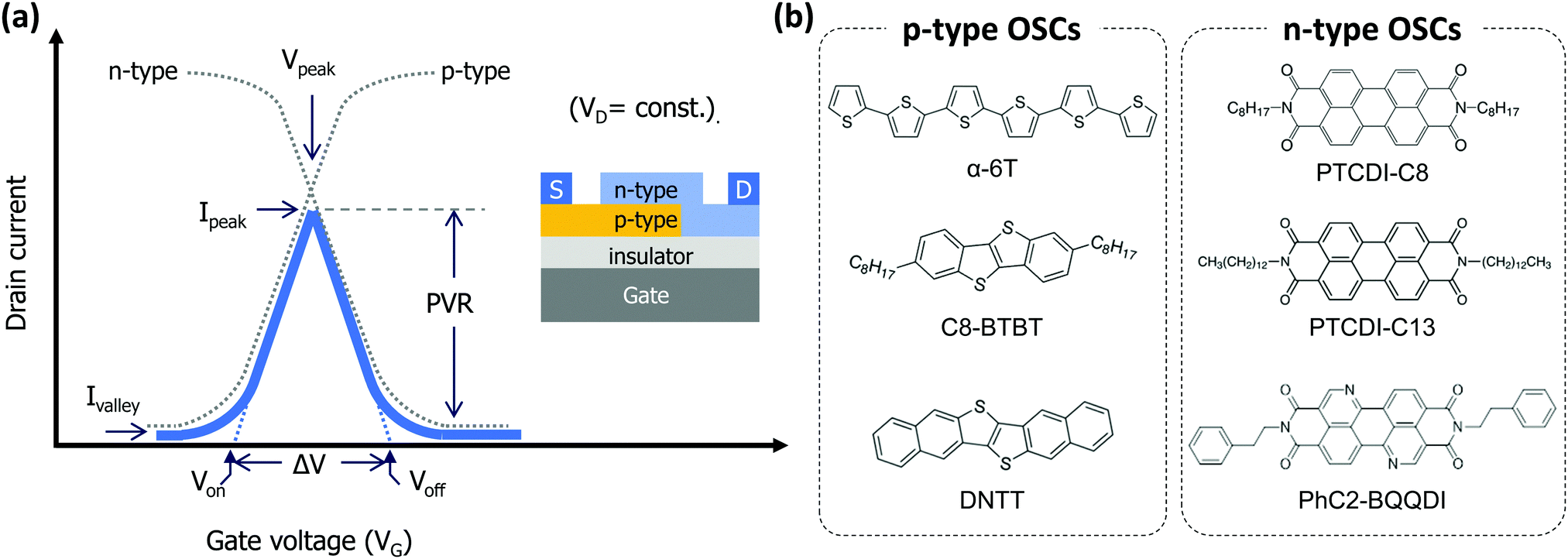 | ||
| Fig. 1 (a) Illustration of the AAT device structure with PN-heterojunction in the transistor channel, and indices to determine the Λ-shaped curve properties. Here, Vpeak is the driving voltage to yield the highest peak current (Ipeak). The peak-to-valley ratio (PVR = Ipeak/Ivalley) is the ratio between Ipeak and the drain current at valley voltage (Ivalley). ΔV is the driving range between the on-set voltage (Von) and off-set voltage (Voff). The dotted curves show the transfer curves of the n-type and p-type channels, respectively. Reprinted with permission from ref. 12 Copyright 2017 American Chemical Society. (b) Typical molecular structures of the p-type and n-type organic semiconductors used in organic AATs. | ||
In the first AAT, reported by Jariwala et al.,13 carbon nanotubes (CNTs) and MoS2 formed the heterojunction. The Au(source)/MoS2(n-type)/CNTs(p-type)/Au(drain) layers on the substrate worked as a PN-diode, the drain current (ID)–drain voltage (VD) curves of which showed rectification characteristics. Importantly, the rectification curves were tunable by the VG to produce Λ-shaped curves in the ID–VG dimension. Therefore, the device was termed a gate-tunable PN-heterojunction diode. Since then, various kinds of AATs have been reported, with OSCs,14–17 atomically thin two-dimensional (2D) materials such as transition metal dichalcogenides (TMDCs),18–23 or their combinations24–26 utilized to form the PN-heterojunctions. These materials have several things in common. First, the heterojunctions are formed by van der Waals interaction, eliminating the lattice mismatch limitation as distinct from covalently bonded interfaces. Second, both the 2D materials and OSCs have broad material options, which is advantageous for arranging the band-alignments at the heterojunctions. Third, the channel materials are intrinsic semiconductors: unlike in conventional Si-based PN-homojunctions, there is no need for mixed carrier dopant, and thus no depletion layer is formed at the interface in the non-biased state. Another common feature is the ambipolar characteristic that both electrons and holes can be transported through the materials. The observed transfer curves show similar characteristics regardless of the constituent materials. However, the detailed carrier transport mechanisms are different. The band-to-band tunneling is mainly responsible in the 2D materials27–29 Meanwhile, drift-diffusion transport, or short-through current, is a key mechanism in the OSCs.14 Another distinct difference between the 2D materials and OSCs is the processability. Most of the 2D materials have been stacked by mechanical exfoliation using adhesive tapes, and this is disadvantageous in terms of device scalability; whereas, organic semiconducting films are produced mainly by vacuum deposition processing through purposely designed shadow masks, which enables systematic control of the device geometries, including the width and length of the channels, the film thickness, and the PN-heterojunction length. Given these strengths, organic AATs have a competitive advantage in terms of expanding the range of device applications, as well as in terms of fundamental physics. Several review articles have summarized the recent developments in 2D-material-based AAT research;30,31 this paper will review organic AATs and their potential as future electronic devices. First, the fundamental operating principles are discussed from experimental and theoretical perspectives. Second, the current ATT applications are summarized, with a focus on multivalued logic (MVL) circuits. Finally, the mechanical flexibility, optical responsivity, and solution processability of organic AATs are discussed as distinctive applications of organic electronics.
2. Fundamentals of antiambipolar transistors
We begin with the origins of the Λ-shaped transfer curve. Numerical analysis performed by Kobashi et al. indicated a similarity between the Λ-shaped transfer curve in AATs and the shoot-through current observed in CMOS inverters.14 They showed that the transient spiky electrical current (Λ-curve) was induced, in switching between p- and n-FET operation, only within a certain range of gate bias voltage (ΔV in Fig. 1). Fig. 2 illustrates this ID dependence on VG using simplified energy-level diagrams.15 Here, α-sexithiophene (α-6T), N,N′-dioctyl-3,4,9,10-perylenedicarboximide (PTCDI-C8), and Au thin films were employed as the p-type, n-type, and source-drain electrodes, respectively. In the low VG range (Fig. 2a), ID was suppressed because the p-FET was in the off-state, even though the n-FET was in the on-state and electrons were injected and transportable in the n-channel. In a similar manner, no ID was observed in the high VG range (Fig. 2c) because the n-FET was in the off-state. Only in the middle VG range, from −30 V to −50 V (Fig. 2b), a sharp increase and decrease in ID was observed because both FETs were in the on-state simultaneously. An essential point of this transistor operation is that the drain electrode (D) works as a source electrode; the electrons are injected only from the drain electrode to the n-type channel (PTCDI-C8) in the gate- and drain–bias voltage conditions in Fig. 2. For instance, the positive gate voltage of +40 V and the drain voltage of +60 V are applied to the n-type channel when the gate and drain voltages of the AAT are −20 V and −60 V, respectively. Therefore, the PTCDI becomes conductive even when the negative gate voltages are applied to the AAT. These results are attributable to the nature of OSCs, which are essentially intrinsic and ambipolar. Although the ambipolarity can be observed in the limited conditions in general, both electrons and holes can be injected and transported, depending on the highest occupied molecular orbital (HOMO)-lowest unoccupied molecular orbital (LUMO) levels and the work function of the electrodes, and owing to the fine balance of the applied bias voltages in the characteristic AAT configuration. Kim et al. supported this scenario with a theoretical insight based on finite-element simulations.32 They analyzed the carrier transport mechanism in terms of the drift or diffusion, depletion or accumulation, of holes and electrons, depending on the VG range. Their simulations were performed by fitting several key parameters, such as the device geometries (channel lengths and film thickness), material properties (HOMO and LUMO levels of the OSCs, dielectric constants of the gate insulators, work function of the electrodes), mobilities of holes and electrons, etc. The experimental data were well reproduced, confirming the reliability of the simulations.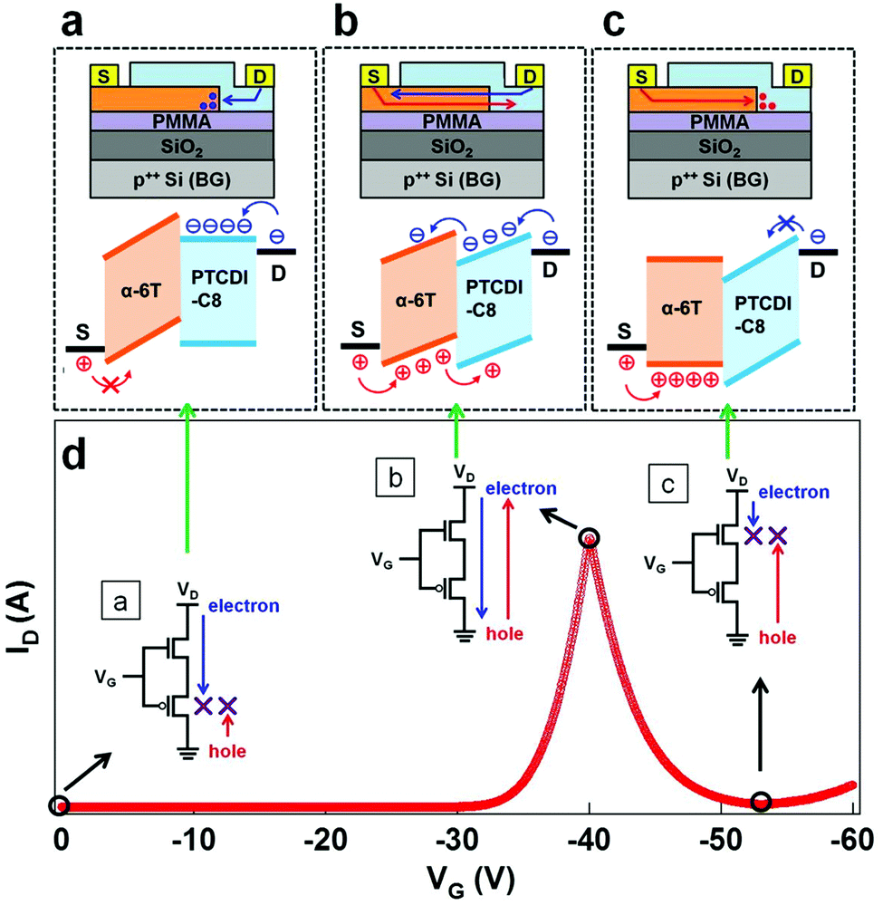 | ||
| Fig. 2 Energy-level alignments at respective VG ranges. (a) The n-FET is in the on-state but the p-FET is in the off-state, therefore no current is induced in the early VG range. (b) Both channels are in the on-state in the middle VG range, to allow both electron and hole transport, resulting in a sharp increase in ID. (c) The n-FET is in the off-state in the high VG range, with the p-FET still in the on-state, causing a rapid decrease in ID, and making the transconductance (dID/dVG) negative. (d) The measured ID–VG curve shows a sharp increase and decrease depending on the VG range, yielding a Λ-shaped curve. The AAT can be regarded as a series connection of the p-type and n-type channels, as illustrated by the schematic circuit diagrams in the inset. Reprinted with permission from ref. 15 Copyright 2022 and ref. 14 Copyright 2017 Wiley-VCH GmbH. | ||
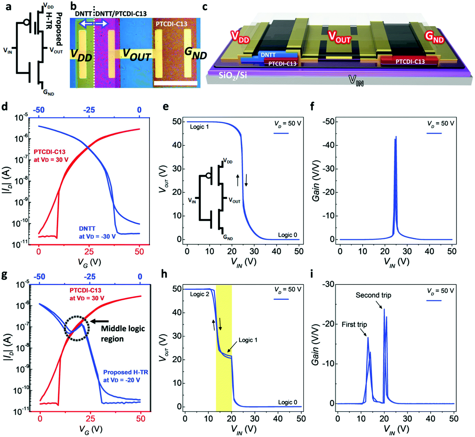
It is important that the threshold voltages of the p- and n-FETs are dominant factors in characterizing the AAT properties. As shown in Fig. 1, Von (Voff) corresponds to the threshold voltage of the p- (n-)FET, and |Voff| > |Von| is a necessary condition to yield the Λ-shaped transfer curve. Based on this fact, Kobashi et al. demonstrated that insertion of the carrier injection layers at the OSC/metal electrode interfaces was an effective way to control Vpeak and ΔV; these parameters correspond to the driving voltage and driving window of the AATs. For example, a MoO3 (Cs2CO3) thin film worked as a hole (electron) injection layer to reduce the threshold voltage of the p–(n-)FET. By focusing on this feature, they successfully reduced Vpeak by inserting Cs2CO3 thin films under both the source and drain electrodes.12 Kim et al. confirmed the significance of threshold voltage by evaluating the temperature dependence of the AAT properties, as shown in Fig. 3.33 In this study, dinaphtho[2,3-b:2′,3′-f]thieno[3,2-b]thiophene (DNTT) and PTCDI-C13 were employed as p-type and n-type OSCs, respectively. Their study showed that the temperature dependencies of the Vpeak and Ipeak were consistent with those of the threshold voltages. The thickness of the semiconductor film also influences the threshold voltage, as demonstrated by Jo et al.,34 who performed two-dimensional finite-element simulations to systematically investigate the impact of film thickness on the threshold voltage. They noted that channel thickness must be optimized to improve device performance.
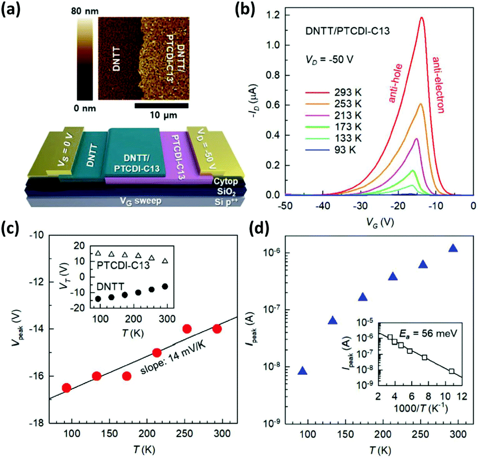 | ||
| Fig. 3 (a) An AFM image of the PN-heterojunction, and an illustration of the AAT with partially overlapping DNTT (p-channel) and PTCDI-C13 (n-channel) films formed on the CYTOP/SiO2/p++-Si substrate. Also, the temperature dependence of (b) the Λ-shaped transfer curves, (c) Vpeak, and (d) Ipeak. These dependencies coincide with those of the threshold voltages of the DNTT and PTCDI-C13 channels. Reprinted with permission from ref. 33 Copyright 2021 Wiley-VCH GmbH. | ||
Other influential parameters on the AAT properties are the channel lengths (Lp and Ln for the p- and n-channels, respectively), and the ratio of Lp/Ln.34,35 Especially as the lateral distribution of the applied VD is determined by these length parameters, the carrier accumulation and depletion in each semiconductor region are strongly affected. In fact, experimental data has confirmed that an optimized Lp/Ln increased Ipeak and reduced Vpeak.16 These controlled experiments were made possible because the OSC films and metal electrodes were produced by the vacuum deposition process, which enabled systematic data acquisition and collaborative analysis based on a theoretical approach. Although single crystalline OSCs enabled high ATT performance, as demonstrated by Liu et al.,36 systematic experimentation and scalability are not yet possible like in the case 2D-material-based AATs.
The next issue to be addressed is the carrier transport path, particularly through the PN-heterojunction. Kobashi et al. noted that there are two possible paths: the vertical interface and the lateral edge junction of the PN-heterojunction, as illustrated in Fig. 4a.16 They conducted controlled experiments by adjusting the device geometries, specifically the thickness of the p-channel (α-6T) and the PN-heterojunction length (ΔL), as shown in Fig. 4b. ΔL was shown to have only a marginal impact on the AAT properties, indicating that the vertical interface could be ruled out in this respect. On the other hand, the Λ-shaped transfer curve was observed even in a device with an extremely thick p-channel, where the n-channel (PTCDI-C8) was completely disconnected at the p-channel edge. Based on these results, they concluded that both electrons and holes were transported through the lateral edge junction. These experimental data were reproduced in theoretical simulations in which no heterojunction length (ΔL = 0) was considered in the calculation.32,35 As one can see in Fig. 5a and the Λ-shaped blue line in Fig. 5c, the AAT characteristics were well reproduced, even though only the lateral edge junction was taken into account in the simulation. These analyses present us with a new challenge: a highly ordered lateral edge junction must be created in order to optimize the device performance. Considerable efforts have thus far been made to design a well-aligned vertical interface, where the molecular orientation in each layer and the flatness of the heterointerface are well defined on the single-layer level.37,38 However, no attention has yet been paid to such fine preparation in the case of the lateral edge junction. This, however, may be good news in disguise, as it suggests that there is considerable room for further improvement in device performance, by focusing on the delicate molecular architectonics at the lateral edge junction.
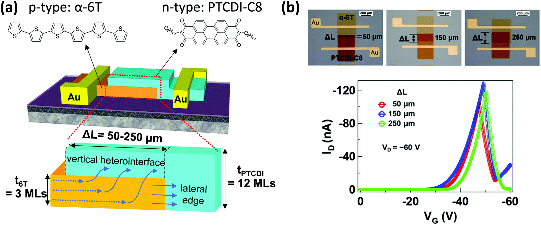 | ||
| Fig. 4 (a) Illustration of an AAT with an α-6T (p-channel) and PTCDI-C8 (n-channel), and an enlarged drawing detecting possible carrier transport paths (vertical heterointerface or lateral edge junction). Geometric dimensions, such as pn-heterojunction overlapping length (ΔL= 50–250 μm) and thicknesses of respective channels (t6T = 3) monolayers (MLs), tPTCDT = 12 monolayers (MLs), were shown in the illustration. (b) Photographs of AATs, with overlapping lengths (ΔL) systematically changed, and the respective transfer curves. Reprinted with permission from ref. 16 Copyright 2018 American Chemical Society. | ||
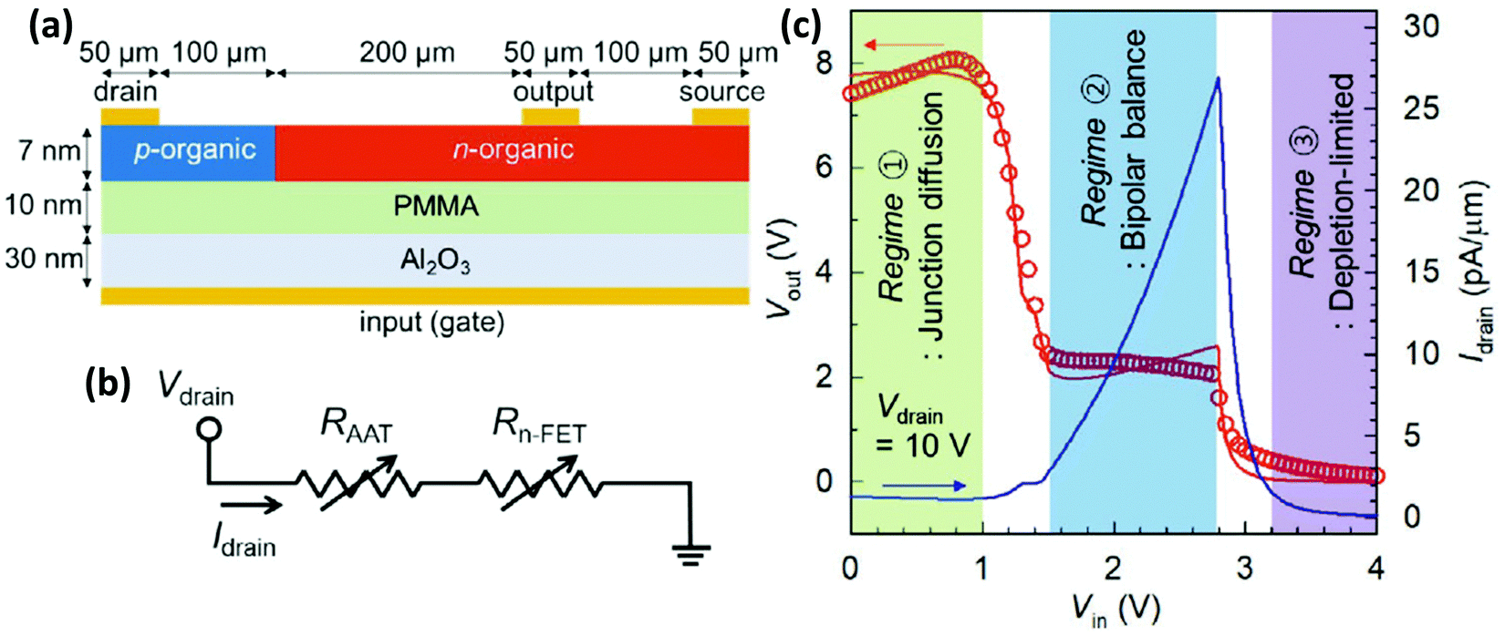 | ||
| Fig. 5 (a) Schematic drawing of the device geometry for simulation. The key dimensions, including the thickness of the OSCs and dielectric layers, the respective channel lengths, and the width of the electrodes, are shown. (b) A simplified circuit model, which is described as a series connection with variable AAT and n-FET resistances. (c) The respective voltage transfer curves obtained by simulation (red circles) and experiment (red line) show high consistency. The blue line shows the measured Λ-shaped transfer. Importantly, the experimental data were well reproduced, even without a vertical heterointerface, indicating that the carriers were transported through the lateral edge junction. Reprinted with permission from ref. 32 Copyright 2020 Wiley-VCH GmbH. | ||
Liu et al. showed that a cross-bar heterojunction also exhibited the Λ-shaped transfer curve, as shown in Fig. 6.36 In this study, high carrier mobilities were achieved due to highly aligned molecular packing in the single crystals. Another improvement can be seen in the hysteresis in the transfer curves. The hysteresis is caused by the shift in the threshold voltages, resulting in the variations in the AAT properties, such as PVR, Vpeak and ΔV. While, the hysteresis in the transfer curve was effectively reduced by a defect-free air-gap dielectric layer. Importantly, these results indicate that a variety of PN-heterojunction configurations are possible for AATs, suggesting the potential for a wide range of device architectures and functionalities. Meanwhile, it should be noted that the cross-bar AAT has only a vertical interface, with no lateral edge junction being formed. Similar cross-bar structures had been reported in the TMDC-based AATs.39,40 It is likely that an alternative carrier transport mechanism (e.g., band-to-band tunneling through the vertical heterointerface, in analogy with 2D-material-based AATs), should be considered to explain the electrical current.
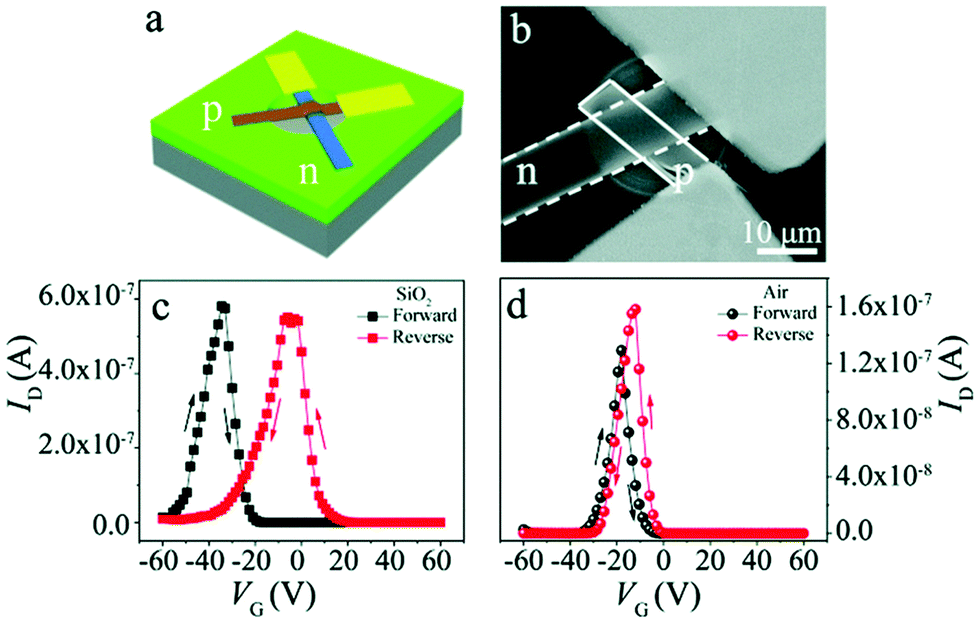 | ||
| Fig. 6 (a) Illustration and (b) photograph of a cross-bar AAT, where the channels consist of single crystalline OSCs of a quinoidal compound and an anthracene derivative. The transfer curves obtained on the (c) SiO2 and (d) air-gap dielectric layers, indicating that the defect-free air-gap interface is effective in reducing hysteresis. Reprinted with permission from ref. 36 Copyright 2020 The Royal Society of Chemistry. | ||
3. Application of antiambipolar transistors: multivalued logic circuits
MVL circuits incorporate more than two logic states. This has the advantage, over the conventional, binary logic devices, that it increases the integral density and reduces the device complexity. Among their other advantages, MVL circuits reduce power consumption and improve data processing speed, due to the reduced interconnection area compared to the conventional binary systems. Owing to these advantages, research on MVL circuits has been increasing since the 1990s (Fig. 7).41,42 This trend is coincident with the looming limitations of Moore's law; however, no feasible device has yet been developed because complicated device integrations are required. The AAT represents a promising device architecture for overcoming this obstacle, due to its distinctive NDT characteristics. MVL circuits have been developed by utilizing AATs with various material combinations: 2D–2D18–21,43 and organic–organic semiconductors.44–46 The device structure of the first organic MVL circuit, reported in 2018,44 is shown in Fig. 8a and b, where the AAT and n-FET are connected in series with four terminals. The rightmost electrode was grounded (GND), and the input voltage (VIN) and supply voltage (VDD) were supplied from the bottom gate and leftmost electrode, respectively. The output voltage (VOUT) was monitored at the central electrode. The ID in the respective transistors were induced independently by VIN. Then, the magnitude relations of the ID in the AAT and n-FET depended on the VIN range (I, II, and III in Fig. 8c). Three levels of output voltage (“1”, “1/2”, “0”) were clearly exhibited as evidence of ternary inverter operation (Fig. 8d). Here, the third logic state (“0”) was produced because of the NDT characteristic of the AAT in Range III. However, this embryonic organic MVL circuit had its share of drawbacks, including high driving voltage, unbalanced three logic states, imperfect output swing and a marginal noise margin for stable operation.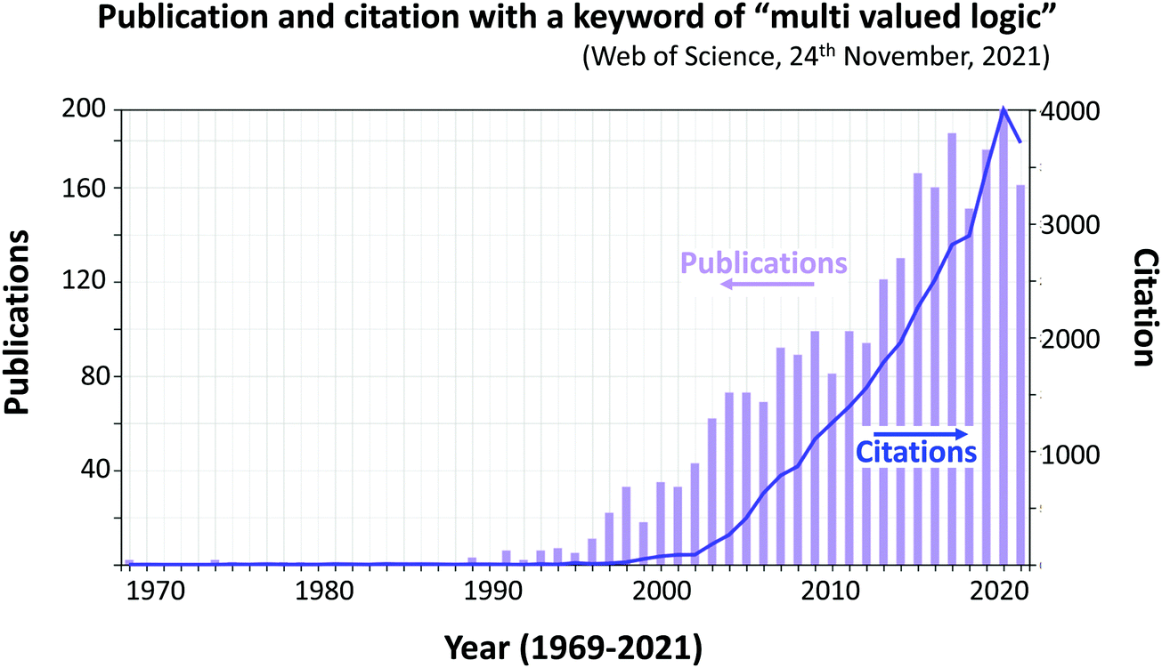 | ||
| Fig. 7 The number of publications and their citations with keyword ‘multivalued logic’ from 1969–2021. | ||
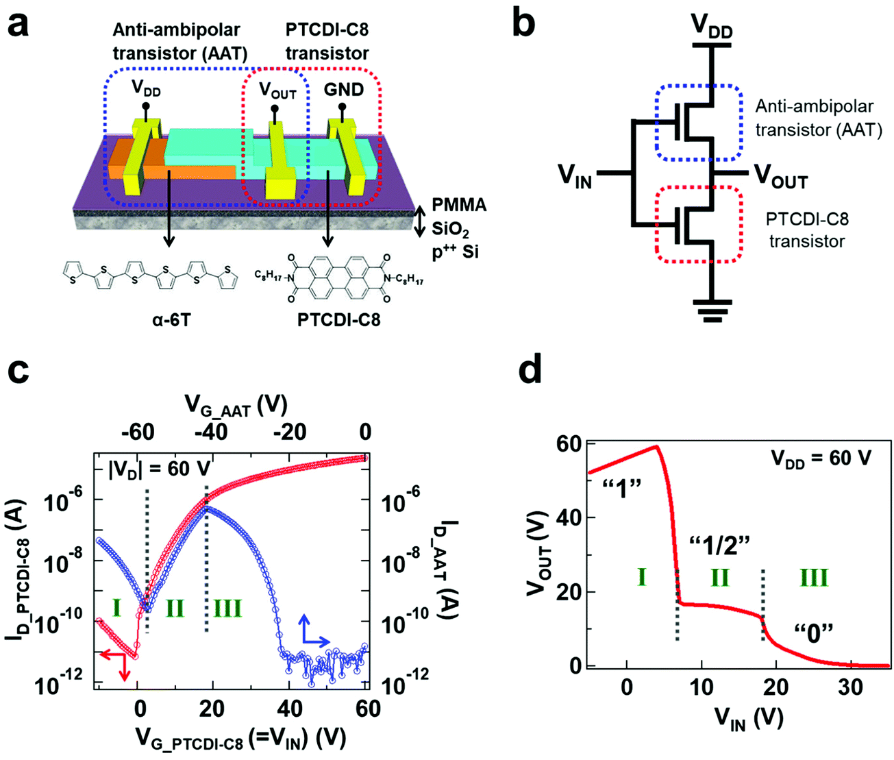 | ||
| Fig. 8 (a) Illustration and (b) schematic diagram of an organic MVL circuit, where the α-6T/PTCDI-C8 AAT and n-FET (PTCDI-C8) are connected in series. (c) ID–VG curves for the n-FET (red) and AAT (blue). (d) Voltage transfer curve (VIN–VOUT), showing ternary inverter operation. Reprinted with permission from ref. 44 Copyright 2018 American Chemical Society. | ||
Yoo et al. tackled these problems by proposing a new device structure.45 Their device was consisted of DNTT and PTCDI-C13 as the p-type and n-type OSCs, respectively. The notable feature of this device was that the DNTT (p-type) channel was connected to both the source and drain electrodes, while the PTCDI-C13 channel was in contact with only one side (source or drain), as shown in Fig. 9a–c. They termed this device a heterojunction transistor. Owing to this geometry, in particular the continuous p-channel, the device showed an N-shaped transfer curve; that is, the drain current increased again above the NDT range with increasing gate bias voltage (blue line in Fig. 9g). As a result, the ternary inverter attained a full VDD-to-GND swing (Fig. 9h). In addition, a polymer layer (CYTOP®) on the SiO2 dielectric layer reduced the hysteresis in the I–V curves and improved reproducibility. Additionally, the DNTT film decreased the contact resistance between the PTCDI-C13 channel and Au electrode to improve the Ion/Ioff ratio, contributing to the full-swing operation.
 | ||
| Fig. 9 (a)–(c) Diagram, illustrations, and photograph of the DNTT/PTCDI-C13 heterojunction and PTCDI-C13(n-channel) transistors. (d) Transfer curves of the respective p-FET (red line) and n-FETs (blue line). (e) Binary VIN–VOUT curve and (f) gain measured in the DNTT/PTCDI inverter. (g) Transfer curves of the n-FET (PTCDI-C13 channel) (red line) and DNTT/PTCDI-C13 heterojunction transistor (blue line, showing “N” shape). (h) Voltage transfer curve and (i) gains measured during ternary inverter operation. Reprinted with permission from ref. 45 Copyright 2019 Wiley-VCH GmbH. | ||
Lee et al. developed a similar heterojunction transistor with the same semiconductor combination (DNTT and PTCDI-C13), but with a different gate electrode and dielectric layer,46 In this work, they pointed out that the intermediate (“1/2”) state had to be well controlled to improve MVL performance. The uniqueness of their device lay in its asymmetric source/drain electrodes, the widths of which were different (narrow or wide), enabling adjustment of the hole and electrode injection (Fig. 10a). Additionally, the channel thicknesses were optimized to control channel conductivity. Through systematic optimization of these factors, they achieved high MVL performance: low voltage operation, full-swing output voltage, three balanced logic states (with the “1/2” state at VDD/2), improved durability, high gain, and high static noise margin (SNM), as demonstrated in Fig. 10b–i. Thanks to these efforts, the performance of the organic MVL circuits has been significantly enhanced in only a few years.
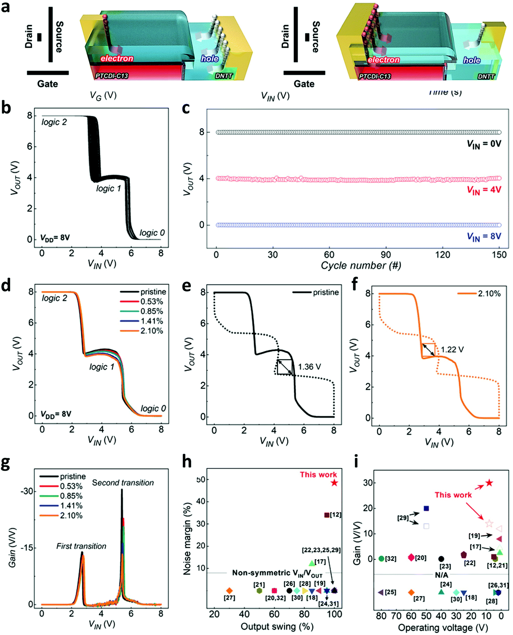 | ||
| Fig. 10 (a) Illustrations of heterojunction transistors with asymmetric source/drain electrodes. (b)–(i) Voltage transfer curves, output voltages, gain, and benchmarks, illustrating the improved performance and excellent mechanical durability. Reprinted with permission from ref. 46 Copyright 2021 Wiley-VCH GmbH. | ||
Theoretical simulations have played a leading role not only in understanding the relevant fundamentals, but also in designing the organic MVL circuit geometries and selecting constituent materials.32,34,35 Kim and his colleagues showed that optimization of the channel thickness (tosc), channel lengths (Lp, Ln), and Lp/Ln ratio was necessary to improve the MVL circuit performance. Fig. 11a and b show the voltage transfer curves (VTCs) and Λ-shaped transfer curves calculated by two-dimensional finite-element simulation. Additionally, special distributions of the carriers (holes and electrons) are visualized in Fig. 11c and d. All these properties showed a clear dependence on Lp/Ln, suggesting the importance of tight optimization of the device geometries, in order to improve the output swing and logic state balance of the VTC. In particular, a dramatic increase in output swing with junction alignment was fully explained by revealing the transition from lateral to vertical charge distribution. In their study, they suggested that there was a contact-depletion effect due to the output node; that is, the holes and electrons could be depleted only through contact with the Au electrode, even given its floating characteristics, and this effect could produce a bottleneck in the carrier transport. In other words, their theoretical analysis implied that appropriate selection of the electrode material (or work function) has the potential to improve device performance.
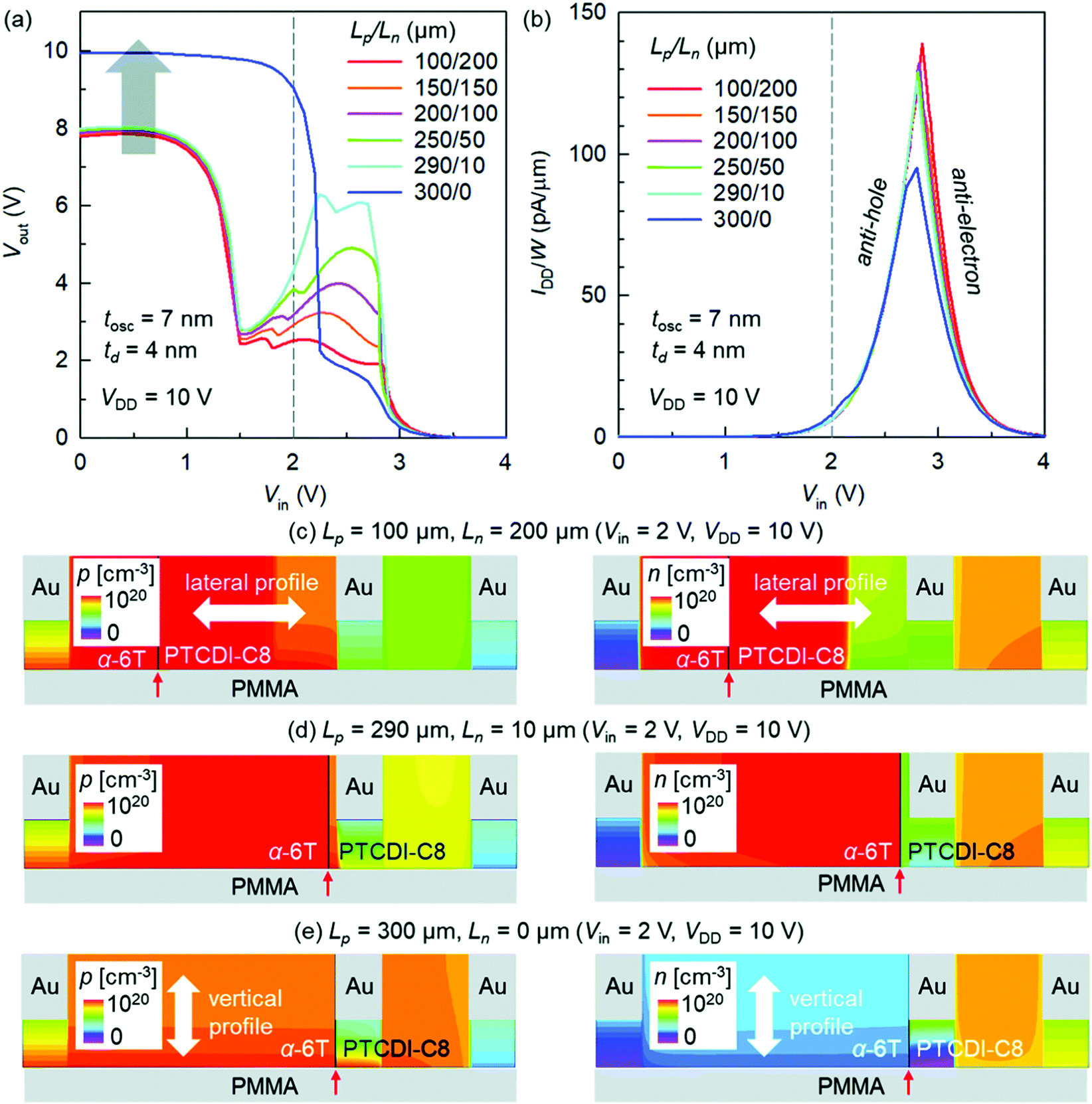 | ||
| Fig. 11 (a) Voltage transfer curves and (b) ID–VIN curves calculated by theoretical simulation, showing clear Lp/Ln dependence. (c)–(e) Spatial distribution of holes (electrons) on the left (right), depending on Lp/Ln. Reprinted with permission from ref. 34 Copyright 2021 The Royal Society of Chemistry. | ||
The study of Jeon et al. is also relevant here,47 though the device structure there is different from that of the AATs. Their device configuration was essentially the same as that of a CMOS inverter, where the p- and n-FETs are connected by a common electrode. Importantly, both channel materials had ambipolar characteristics; the difference lay in the dominant carrier: hole or electron. The transfer characteristics showed a double-peak N-shape curve, yielding negative transconductance in certain ranges of input voltage. As a result, ternary inverter operation was achieved. These results were owing to the features of the OSCs, which are essentially intrinsic and ambipolar, meaning that both electrons and holes can be injected and transported depending on the HOMO–LUMO levels and the work function of the electrodes.
4. Application of antiambipolar transistors: optical responsivity, device flexibility, solution processability
A variety of ATT applications have been proposed, with the deepening of our fundamental understanding and advances in the device fabrication process. A typical evolution can be seen in the case of the light irradiation effect on the AAT properties. Various light irradiation effects have thus far been reported in the 2D-material-based AATs; for example, the photovoltaic effect at the PN-heterojunction (Fig. 12a),48–50 self-driven photoswitching,51 photo-induced carrier doping52 (Fig. 12b), and the light-triggered ternary inverter (Fig. 12c).53 In terms of the light irradiation effect, organic AATs are advantageous owing to the high light responsivity (or light absorbance) of the OSCs compared with the 2D counterparts. Recently, Debdatta et al. reported that light irradiation enabled fine tuning of the VTCs of MVL circuits.54 In particular, the light wavelength was found to be a controlling parameter for adjusting ternary logic states, owing to the distinct absorption spectra of the p- and n-type OSCs. Exploiting similar features, Kim et al. developed a multi-parameter light detector.55Fig. 13 shows that the Λ-shaped transfer curves are sensitively modified by the irradiation location and wavelength. This light detection capability is owing to the device structure, with its partially overlapping PN-heterojunction, and the distinct light absorbances of the constituent OSCs (DNTT and PTCDI-C13).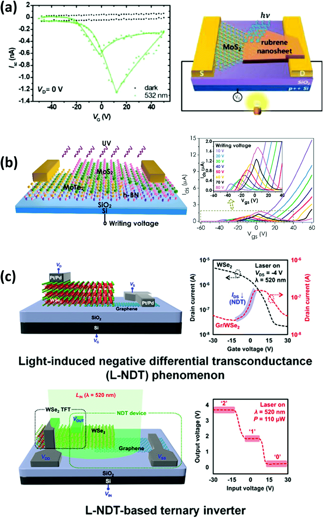 | ||
| Fig. 12 Light irradiation effects on 2D-material-based AATs: (a) photovoltaic effect in a pentacene/MoS2 ATT, Reprinted with permission from ref. 48 Copyright 2018 American Chemical Society. (b) Photo-induced carrier doping in an MoS2/MoTe2 ATT, Reprinted with permission from ref. 52 Copyright 2019 American Chemical Society. (c) Light-triggered NDT and MVL in a WSe2/graphene AAT. Reprinted with permission from ref. 53 Copyright 2017 American Chemical Society. | ||
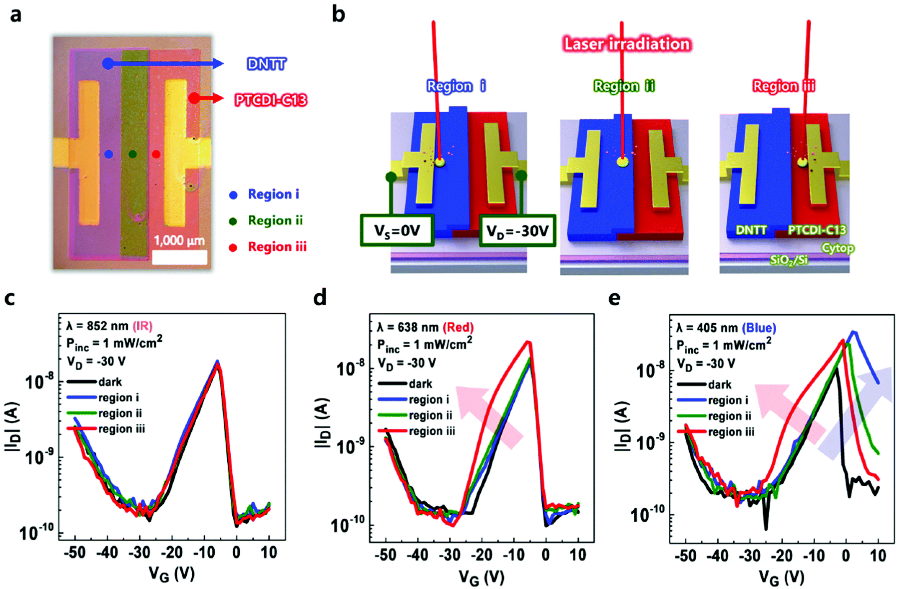 | ||
| Fig. 13 Light-induced variation in the transfer curve, depending on the irradiation location and wavelength. (a) Photograph and (b) illustrations of a DNTT/PTCDI-C13 AAT. The respective transfer curves under light irradiation at various locations (Region i, ii, or iii in (a), and (VIN–VOUT) in (b)) with wavelength of (c) 852 nm, (d) 638 nm, and (e) 405 nm. Reprinted with permission from ref. 55 Copyright 2021 Elsevier. | ||
The above-mentioned devices were basically produced using vacuum deposition processes. It is generally recognized that solution (or printing) processability is a great advantage of organic electronics. This feature must be extended to the organic AATs. However, thus far, the AATs produced by the solution process have been not reported. For example, the material combinations for the PN-heterojunctions are limited to CNTs with oxide semiconductors56,57 or CNTs with MoS2.13 The organic inverter reported by Jeon et al.47 is notable in this regard. The constituent materials, including the p- and n-channels and dielectric layer, are polymeric materials, suggesting that organic MVL circuits may be producible through solution processing in a manner similar to that of other organic electronic devices. However, it should be noted that this device has no PN-heterojunction. This fact implies that the bottleneck hindering the solution processability of AATs may be ascribable to difficulty in the formation of the PN-heterojunction; it is difficult, for example, to stack soluble OSCs with sharp and flat heterojunctions. Consequently, appropriate selection of the OSCs, which are soluble in different solvents, is essential to achieving solution processability in the case of organic AATs.
Another merit of the organic electronics is that the devices can be produced on lightweight and mechanically flexible substrates. The first flexible AAT was reported by Debdatta et al.,58 who developed an organic ternary inverter on a polyethylene naphthalate (PEN) substrate, with poly(methyl methacrylate) (PMMA) and hafnium oxide (HfO2) used as the gate dielectric layers, the PMMA single dielectric layer being advantageous in terms of mechanical flexibility. The PMMA/HfO2 double dielectric layer achieved low-voltage operation, with some sacrifice of flexibility. Fig. 14a shows the device structure and constituent materials, a photograph of a setup for the bending test, and the mechanical durability of the ternary inverter. Even after 100 bending cycles, the device showed stable and repeatable operation. Soon after this study, a remarkably advanced flexible MVL circuit was reported by Lee et al.46Fig. 14b shows a schematic diagram and photographs of the ternary inverters produced on a very thin PEN substrate. They improved on several advantages of the AATs, with full-swing output voltage, balanced ternary logic states, mechanical durability, and a high SNM.
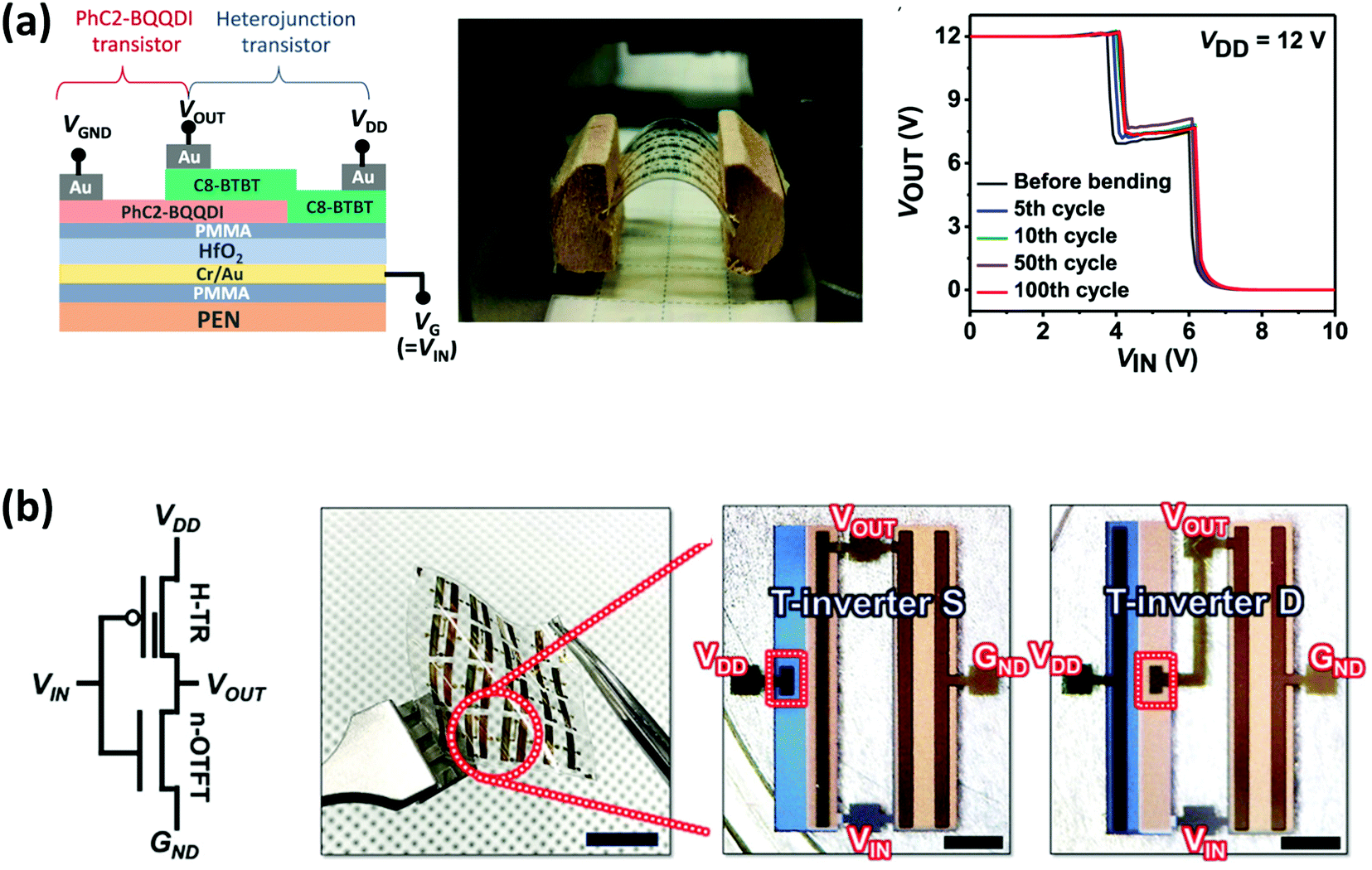 | ||
| Fig. 14 Performance, illustration, and photographs of flexible MVL circuits produced on plastic substrates. (a) Reprinted with permission from ref. 58 Copyright 2021 The Japan Society of Applied Physics (b) reprinted with permission from ref. 46 Copyright 2021 Wiley-VCH GmbH. | ||
5. Conclusion and future perspectives
Summary
This brief review focused on the recent progress in the development of organic AATs. In terms of the fundamentals of the carrier transport mechanism, which were the initial focus of the discussion, our basic understanding has been advancing based equally on theoretical and experimental progress. MVL circuits and optoelectronic functions were then discussed as typical ATT applications. The former based on the distinct NDT feature of ATTs, and the latter on the characteristic transistor structure with its PN-heterojunction. Both show considerable potential as novel organic electronic devices.Future tasks
ATT research is still in the exploratory stage. Therefore, further efforts must be made to elucidate the critical details, such as the band-alignments at the PN-heterojunction and the particular distribution of the electrical field and carrier concentration, especially during device operation. Operando-analysis, that is, the real-time measurement of electrical properties when the devices are in operation under bias voltages, will be effective for this purpose.Appropriate selection of the OSCs is necessary for effective applications because the band-offsets at the PN-heterojunction are key factors in determining the carrier transport. Such band-engineering has become well established in the development of OLEDs, and in an analogous manner, is a critical requirement for AAT applications. Tight optimization of the device geometric parameters is also necessary to maximize the potential of the AATs. Then, theoretical prediction will play a key role in providing guidelines for improving device performance, while another challenging task is the formation of highly ordered interfaces at the lateral edge junctions. Any processes based on vacuum deposition, solution processing or patterning techniques must be designed with the latter task in mind. Thus far, however, such processes remain largely unexplored with respect to organic AATs.
Future potential
As aforementioned, the Λ-shaped transfer curve is a key property of AATs. Recently, advanced types of transfer curves, such as N-shaped and double-peak N-shaped (i.e., W-shaped) curves, have been achieved for improved MVL circuit design. A double-peak Λ-shape (i.e., M-shape) curve may also be possible with the development of highly advanced AAT device architectures. In this way, ‘transfer curve-engineering’ is essential for realizing the potential of AATs, in quaternary logic circuits for example.59–61 In sum, the development of organic AATs represents a promising first step toward opening new frontiers for functional organic electronics.Conflicts of interest
There are no conflicts of interest.Acknowledgements
This research was supported by the World Premier International Center (WPI) for Materials Nanoarchitectonics (MANA), of the National Institute for Materials Science (NIMS), Tsukuba, Japan and JSPS Kakenhi Grant numbers 19H00866 and 21F21052.References
- G. Hong, X. Gan, C. Leonhardt, Z. Zhang, J. Seibert, J. M. Busch and S. Bräse, Adv. Mater., 2021, 33, 2005630 CrossRef CAS PubMed.
- L. J. Sutherland, H. C. Weerasinghe and G. P. Simon, Adv. Energy Mater., 2021, 11, 2101383 CrossRef CAS.
- H. Li, W. Shi, J. Song, H.-J. Jang, J. Dailey, J. Yu and H. E. Katz, Chem. Rev., 2019, 119, 3–5 CrossRef CAS PubMed.
- Y. Wang, J. Zhang, S. Zhang and J. Huan, Polym. Int., 2021, 70, 414–425 CrossRef CAS.
- S. Zhang, Y. Zhao, X. Du, Y. Chu, S. Zhang and J. Huang, Small, 2019, 15, 1805196 CrossRef PubMed.
- T. Leydecker, Z. M. Wang, F. Torricelli and E. Orgiu, Chem. Soc. Rev., 2020, 49, 7627–7670 RSC.
- Y. Yan, Y. Zhao and Y. Liu, J. Polym. Sci., 2021, 1–17 Search PubMed.
- L. Esaki, Phys. Rev., 1958, 109, 603–604 CrossRef CAS.
- M. Yamamoto, Y. Azuma, M. Sakamoto, T. Teranishi, H. Ishii, Y. Majima and Y. Noguchi, Sci. Rep., 2017, 7, 1589 CrossRef PubMed.
- Y. Wang, W.-X. Zhou, L. Huang, C. Xia, L.-M. Tang, H.-X. Deng, Y. Li, K.-Q. Chen, J. Li and Z. Wei, 2D Mater., 2017, 4, 025097 CrossRef.
- Z. Wang, X. He, X.-X. Zhang and H. N. Alshareef, Adv. Mater., 2016, 28, 9133–9141 CrossRef CAS PubMed.
- K. Kobashi, R. Hayakawa, T. Chikyow and Y. Wakayama, ACS Appl. Mater. Interfaces, 2018, 10, 2762–2767 CrossRef CAS PubMed.
- D. Jariwala, V. K. Sangwan, C.-C. Wu, P. L. Prabhumirashi, M. L. Geier, T. J. Marks, L. J. Lauhona and M. C. Hersama, Proc. Natl. Acad. Sci. U. S. A., 2013, 110, 18076–18080 CrossRef CAS PubMed.
- K. Kobashi, R. Hayakawa, T. Chikyow and Y. Wakayama, Adv. Electron. Mater., 2017, 3, 1700106 CrossRef.
- R. Hayakawa, K. Honma, S. Nakaharai, K. Kanai and Y. Wakayama, Adv. Mater., 2022, 2109491 CrossRef CAS PubMed.
- K. Kobashi, R. Hayakawa, T. Chikyow and Y. Wakayama, J. Phys. Chem. C, 2018, 122, 6943–6946 CrossRef CAS.
- S. On, Y.-J. Kim, H.-K. Lee and H. Yoo, Appl. Surf. Sci., 2021, 542, 148616 CrossRef CAS.
- J. Shim, S. Oh, D.-H. Kang, S.-H. Jo, M. H. Ali, W.-Y. Choi, K. Heo, J. Jeon, S. Lee, M. Kim, Y. J. Song and J.-H. Park, Nat. Commun., 2016, 7, 13413 CrossRef CAS PubMed.
- M. Huang, S. Li, Z. Zhang, X. Xiong, X. Li and Y. Wu, Nat. Nanotechnol., 2017, 12, 1148–1155 CrossRef CAS PubMed.
- P. K. Srivastava, Y. Hassan, Y. Gebredingle, J. Jung, B. Kang, W. J. Yoo, B. Singh and C. Lee, Small, 2019, 15, 1804885 CrossRef PubMed.
- Y. Hassan, P. K. Srivastava, B. Singh, M. S. Abbas, F. Ali, W. J. Yoo and C. Lee, ACS Appl. Mater. Interfaces, 2020, 12, 14119–14124 CrossRef CAS PubMed.
- H. Yao, E. Wu and J. Liu, Appl. Phys. Lett., 2020, 117, 123103 CrossRef CAS.
- D. Wu, W. Li, A. Rai, X. Wu, H. C. P. Movva, M. N. Yogeesh, Z. Chu, S. K. Banerjee, D. Akinwande and K. Lai, Nano Lett., 2019, 19, 1976–1981 CrossRef CAS PubMed.
- D. Jariwala, S. L. Howell, K.-S. Chen, J. Kang, V. K. Sangwan, S. A. Filippone, R. Turrisi, T. J. Marks, L. J. Lauhon and M. C. Hersam, Nano Lett., 2016, 16, 497–503 CrossRef CAS PubMed.
- J.-K. Kim, K. Cho, T.-Y. Kim, J. Pak, J. Jang, Y. Song, Y. Kim, B. Y. Choi, S. Chung, W.-K. Hong and T. Lee, Sci. Rep., 2016, 6, 36775 CrossRef CAS PubMed.
- K.-S. Jung, K. Heo, M.-J. Kim, M. Andreev, S. Seo, J.-O. Kim, J.-H. Lim, K.-H. Kim, S. Kim, K. S. Kim, G. Y. Yeom, J. H. Cho and J.-H. Park, Adv. Sci., 2020, 7, 2000991 CrossRef CAS PubMed.
- T. Roy, M. Tosun, X. Cao, H. Fang, D.-H. Lien, P. Zhao, Y.-Z. Chen, Y.-L. Chueh, J. Guo and A. Javey, ACS Nano, 2015, 9, 2071–2079 CrossRef CAS PubMed.
- S. Fan, Q. A. Vu, S. Lee, T. L. Phan, G. Han, Y.-M. Kim, W. J. Yu and Y. H. Lee, ACS Nano, 2019, 13, 8193–8201 CrossRef CAS PubMed.
- X. Xiong, J. Kang, Q. Hu, C. Gu, T. Gao, X. Li and Y. Wu, Adv. Funct. Mater., 2020, 30, 1909645 CrossRef CAS.
- Y. Wakayama and R. Hayakawa, Adv. Funct. Mater., 2020, 30, 1903724 CrossRef CAS.
- M. E. Beck and M. C. Hersam, ACS Nano, 2020, 14, 6498–6518 CrossRef CAS PubMed.
- C.-H. Kim, R. Hayakawa and Y. Wakayama, Adv. Electron. Mater., 2020, 6, 1901200 CrossRef CAS.
- C.-H. Kim and H. Yoo, Adv. Electron. Mater., 2021, 7, 2100167 CrossRef CAS.
- S.-W. Jo, J. Choi, R. Hayakawa, Y. Wakayama, S. Jung and C.-H. Kim, J. Mater. Chem. C, 2021, 9, 15415–15421 RSC.
- H. Yoo and C.-H. Kim, IEEE Electron Device Lett., 2021, 42, 1323–1326 CAS.
- J. Liu, J. Liu, J. Zhang, C. Li, Q. Cui, F. Teng, H. Li and L. Jiang, J. Mater. Chem. C, 2020, 8, 4303–4308 RSC.
- N. Hiroshiba, J. P. Hill, R. Hayakawa, K. Ariga, K. Matsuishi and Y. Wakayama, Thin Solid Films, 2014, 554, 74–77 CrossRef CAS.
- E. Barrena, D. G. de Oteyza, S. Sellner, H. Dosch, J. O. Ossó and B. Struth, Phys. Rev. Lett., 2006, 97, 076102 CrossRef PubMed.
- N. T. Duong, J. Lee, S. Bang, C. Park, S. C. Lim and M. S. Jeong, ACS Nano, 2019, 13, 4478–4485 CrossRef CAS PubMed.
- J. Y. Kim, H. J. Park, S.-H. Lee, C. Seo, J. Kim and J. Joo, ACS Appl. Mater. Interfaces, 2020, 12, 36530–36539 CrossRef CAS PubMed.
- H. Yoo and C.-H. Kim, J. Mater. Chem. C, 2021, 9, 4092–4104 RSC.
- S. B. Jo, J. Kang and J. H. Cho, Adv. Sci., 2021, 8, 2004216 CrossRef CAS PubMed.
- R. Hu, E. Wu, Y. Xie and J. Liu, Appl. Phys. Lett., 2019, 115, 073104 CrossRef.
- K. Kobashi, R. Hayakawa, T. Chikyow and Y. Wakayama, Nano Lett., 2018, 18, 4355–4359 CrossRef CAS PubMed.
- H. Yoo, S. On, S. B. Lee, K. Cho and J.-J. Kim, Adv. Mater., 2019, 31, 1808265 CrossRef PubMed.
- C. Lee, J. Choi, H. Park, C. Lee, C.-H. Kim, H. Yoo and S. G. Im, Small, 2021, 17, 2103365 CrossRef CAS PubMed.
- J. Jeon, M. J. Kim, G. Shin, M. Lee, Y. J. Kim, B. S. Kim, Y. Lee, J. H. Cho and S. Lee, ACS Appl. Mater. Interfaces, 2020, 12, 6119–6126 CrossRef CAS PubMed.
- C.-J. Park, H. J. Park, J. Y. Lee, J. Kim and J. Joo, ACS Appl. Mater. Interfaces, 2018, 10, 29848–29856 CrossRef CAS PubMed.
- A. M. Afzal, M. Z. Iqbal, S. Mumtaz and I. Akhtarc, J. Mater. Chem. C, 2020, 8, 4743–4753 RSC.
- Y. Sun, W. Gao, X. Li, C. Xia, H. Chen, L. Zhang, D. Luo, W. Fan, N. Huo and J. Li, J. Mater. Chem. C, 2021, 9, 10372–10380 RSC.
- N. Huo, J. Yang, L. Huang, Z. Wei, S.-S. Li, S.-H. Wei and J. Li, Small, 2015, 11, 5430–5438 CrossRef CAS PubMed.
- E. Wu, Y. Xie, Q. Liu, X. Hu, J. Liu, D. Zhang and C. Zhou, ACS Nano, 2019, 13, 5430–5438 CrossRef CAS PubMed.
- J. Shim, S.-H. Jo, M. Kim, Y. J. Song, J. Kim and J.-H. Park, ACS Nano, 2017, 11, 6319–6327 CrossRef CAS PubMed.
- D. Panigrahi, R. Hayakawa, K. Fuchii, Y. Yamada and Y. Wakayama, Adv. Electron. Mater., 2020, 7, 2000940 CrossRef.
- S. Kim, S. Hong and H. Yoo, Sens. Actuators, A, 2021, 330, 112888 CrossRef CAS.
- D. Jariwala, V. K. Sangwan, J.-W. T. Seo, W. Xu, J. Smith, C. H. Kim, L. J. Lauhon, T. J. Marks and M. C. Hersam, Nano Lett., 2015, 15, 416–421 CrossRef CAS PubMed.
- B. Kim, Adv. Electron. Mater., 2020, 6, 2000426 CrossRef CAS.
- D. Panigrahi, R. Hayakawa, K. Honma, K. Kanai and Y. Wakayama, Appl. Phys. Express, 2021, 14, 081004 CrossRef CAS.
- J.-H. Lim, J. Shim, B.-S. Kang, G. Shin, H. Kim, M. Andreev, K.-S. Jung, K.-H. Kim, J.-W. Choi, Y. Lee and J.-H. Park, Adv. Funct. Mater., 2019, 29, 1905540 CrossRef CAS.
- M. Andreev, J.-W. Choi, J. Koo, H. Kim, S. Jung, K.-H. Kim and J.-H. Park, Nanoscale Horiz., 2020, 5, 1378–1385 RSC.
- K.-H. Kim, H.-Y. Park, J. Shim, G. Shin, M. Andreev, J. Koo, G. Yoo, K. Jung, K. Heo, Y. Lee, H.-Y. Yu, K. R. Kim, J. H. Cho, S. Leeagan and J.-H. Park, Nanoscale Horiz., 2020, 5, 654–662 RSC.
| This journal is © The Royal Society of Chemistry 2022 |