
 Open Access Article
 This Open Access Article is licensed under a Creative Commons Attribution-Non Commercial 3.0 Unported Licence
Synthesis, modification, and application of black phosphorus, few-layer black phosphorus (FLBP), and phosphorene: a detailed review
Nasrin
Sultana
 ab,
Annabelle
Degg
c,
Samiran
Upadhyaya
a,
Tom
Nilges
c and
Neelotpal
Sen Sarma
*a
ab,
Annabelle
Degg
c,
Samiran
Upadhyaya
a,
Tom
Nilges
c and
Neelotpal
Sen Sarma
*a
aInstitute of Advanced Study in Science and Technology, Paschim Boragaon, Guwahati-35, Assam, India. E-mail: neelot@iasst.gov.in
bAcademy of Scientific and Innovative Research (AcSIR), Ghaziabad-201002, India
cTechnical University of Muenchen, Lichtenbergstr.4, 85748 Garching, Germany
First published on 31st May 2022
Abstract
In the last few years, new two-dimensional (2-D) materials have garnered the scientific community's attention with the growing demand for functionalized materials for advanced electrical and biomedical applications. Among all the developed 2-D materials, black phosphorus and FLBP (few-layer black phosphorus), i.e., phosphorene, has been in tremendous demand due to its unique electrical, optical, physical, and electrochemical properties. Its tunable bandgap enables the fabrication of sensing materials that could be utilized in various fields such as health care, batteries, transistors, photovoltaics (PV) and many more probable applications. However, properties like high conductivity, carrier mobility, tensile strength, and bio-safety make phosphorene an essential candidate for electrical and bio-medical applications. The present review highlights phosphorene's unique properties, potential applications, and prospects as an emerging 2-D single elemental material. A particular focus has been laid on the most recent studies on the synthetic approaches and modifications of phosphorene, mainly aimed at its functionalization and stabilization for prospective applications in different fields.
1. Introduction
Over the last decade, there has been a sharp growth in the use of 2-D nanomaterials in electronics, sensing, dye degradation, and different biomedical applications, including targeted drug delivery, hyperthermia induced photo-ablation therapy, bio-imaging, and bio-sensors.1,2 In recent years, after the first isolation of graphene an enormous number of reports have been published related to 2-D layered materials ranging from protective coating to biochemical sensing. Until a few years ago, graphene was the only material comprising a single element that exhibited outstanding electronic and mechanical properties, and carrier transport, leading to restructuring in different technological areas. But the lack of a bandgap in graphene limited its use in electronic devices and their fabrication. With the efforts of researchers around the globe, phosphorene as a newly emerging 2-D material, also known as mono or few-layer black phosphorus (FLBP), was developed. Phosphorene is also a single-elemental 2-D material and can be synthesized from black phosphorus. The layers of BP are held together by the weak van der Waals forces which makes it a valuable source for producing free-standing 2-D nanosheets. It can serve as a supporting substrate or an active sensing element in different fields, such as health care. In addition, it is also a favorable material for other applications, such as batteries, transistors, and photovoltaics (PV).3 It is an emerging competitor to other 2-D materials, as it is a p-type semiconductor and can be used in optoelectronics and semiconductor-based devices.4–17 The bandgap value of FLBP depends on the manifold stacking layers (i.e., bulk ∼0.3 eV, bilayer ∼1.88 eV, and mono layer ∼2.0 eV), which could be functionalized and attuned to the desired application.18 It has also attracted enormous interest because of its superior physical properties, such as high mechanical strength, desirable photo-electronic performance, and excellent biocompatibility. The most desirable advantage of phosphorene over other 2-D materials is its in vivo biodegradability, i.e., it can be degraded inside the human body, making it a potential candidate for drug delivery.19 Due to the tunable bandgap, broad absorption across the ultraviolet, visible light, and infra-red regions is possible. So, it can allow colorimetric and fluorescence detection of various types of bio-analytes like proteins, inorganic ions, and DNA. Phosphorene can be considered as one of the most ideal materials for device fabrication compared to other contemporary materials.Recent studies have revealed the potential applications of phosphorene in various fields. Zhang et al. have theoretically shown that phosphorene can easily pass through the cell membrane and extract many phospholipids from it, thereby inducing membrane degradation and reducing cell viability.20 Dharani et al. demonstrated phosphorene as a sensing material to detect the presence of chronic obstructive pulmonary disease (COPD) biomarker volatiles.21 Liang et al. developed a biosensor by synthesizing phosphorene stabilized with a coating of hexamethylenediamine (HMA), which exhibited a concentration-dependent response to 3,3′,4,4′-polychlorinated biphenyl (PCB77).22 Qiu et al., in their review, described the various aspects and applications of phosphorene in biomedical fields, such as bio-imaging, photothermal therapy (PTT), photodynamic therapy (PDT), and combination strategies.18 Although the properties and application of phosphorene have been a topic of immense interest in recent times, minimal studies on its applications have been performed. Most of the recent reviews have been primarily focused on the structural aspects of phosphorene, but detailed analysis of the physico–chemical properties is of utmost importance23–29 and is still awaited.
To understand the overall structural properties and explore potential future applications, detailed insight into the various aspects of phosphorene is necessary, including biological and electronic aspects. This review presents a detailed analysis of the recent advantages of 2-D materials in health care and bio-sensing applications ranging from neural interfacing to therapeutic to wearable devices. This review mainly focuses on (i) a comprehensive estimation of different properties over a wide range of 2-D systems, (ii) a comparison of biosensors based on 2-D materials, and (iii) mass production and commercialization.
2. Outline of 2-D phosphorene
2.1. Structural features and properties
Over the last few years, there has been growing interest in recognizing the comparative properties of BP for further experimental and theoretical research. After its first synthesis in 1914, the fundamental properties of BP such as density, specific heat capacity and electrical conductivity were determined subsequently. Hultgren and Gindrich specified the lattice and crystal structure parameters of BP.30 After almost two decades, Keyes determined the electrical conductivity of BP up to 350 °C and 8000 kg cm−2 as a function of temperature and pressure.31 According to the study, it was found that as an intrinsic semiconductor, BP has a bandgap of about 0.33 eV at high temperatures. In the 1980s, researchers from Japan were able to form a large single crystal from melted red phosphorus under high pressure, using wedge-type cubic anvil apparatus, cooling down slowly under high pressure;32 this paved the way for the study of the optical and electrical properties of BP. Large single crystals of BP up to 10 mm lateral size suitable for a top-down synthesis of phosphorene can be grown by short way transport.33,34 Today, the majority of commercially available BP and phosphorene in a top-down fabrication process is still produced by this route despite various other top-down and bottom-up approaches.The chemical properties of BP were initially predicted using quantum chemical calculations,35–38 followed by multiple experiments. Scientists have been investigating different fascinating characteristics of BP such as mechanical stability,38 optoelectronic features, electrical conductance,39 anisotropic features, layer-dependent bandgap variation, etc.40,41
A detailed description of the research on the study of fundamental properties and phosphorene status is presented in the following sections.
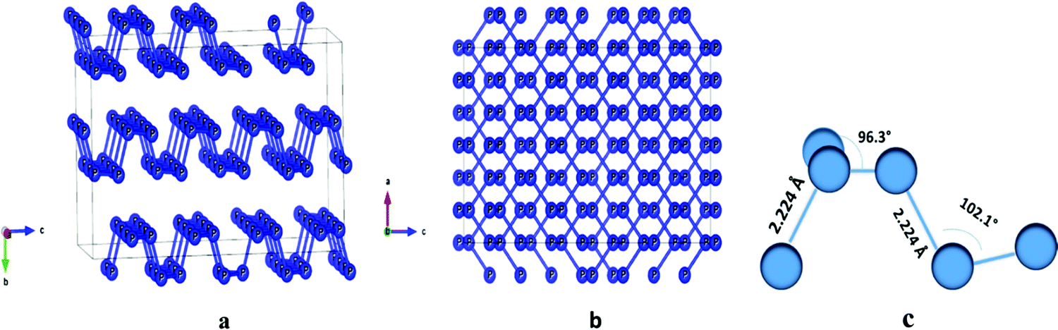 | ||
| Fig. 1 (a) The crystal structure of BP; (b) crystal structure view along the b-axis; (c) bond length and bond angles of phosphorene.47 | ||
Phosphorene as a field-effect transistor (FET) shows an ON/OFF ratio of about 103–105. However, the measured thermal conductivities of phosphorene for an infinite length zig-zag and armchair sheets are 36 W m−1 K−1 and 110 W m−1 K−1, respectively,54 which are lower than those of graphene. The properties of different 2-D materials are presented in Table 1.
| 2D materials | Band gap (eV) | Carrier mobility (cm2 m−1 S−1) | ON/OFF ratio | Thermal conductance (W m−1 K−1) | Thermoelectric performance, ZT | Young's modulus (N m−2) | Features strain (%) | Conductance type |
|---|---|---|---|---|---|---|---|---|
| Phosphorene (semiconductor)50–52,54–58 | 0.3–0.2 | ∼1000 | 103–105 | 10–36 | 1–2.5 | 35–166 | 24–32 | p-Type |
| Graphene (semiconductor)52,58,59–64 | 0 | ∼2 × 10⁵ | 5.5–44 | 5 × 10³ | ∼0 | 1000 | 27–38 | Ambipolar |
| MoS2 (semiconductor)52,58,65–70 | 1.2–1.8 | 10–200 | 106–108 | 34.5–52 | 0.4 | 270 ± 100 | 25–33 | n-Type |
| WSe2 (semiconductor)58,65,71–77 | 1.2 | 140–500 | 104–106 | 9.7 | 0.91 | 75–195 | 26–37 | Ambipolar |
| h-BN (insulator)58,78–80 | 1.7 | — | 250–360 | — | 220–880 | 24 | — |
Phosphorene's high electrical and low thermal conductivities make it a promising material for thermoelectric devices. Its optical absorption primarily depends on its structural orientation. He et al., in their paper, suggested that the most significant absorption and diffusion coefficients of phosphorene are ∼10 and ∼16 times in the armchair direction, which are greater than those in any other direction.81
In a recent review, Rahman et al. predicted phosphorene as an ideal material for water splitting dynamics application and discussed the stability of the material when exposed to water, light, air, and temperature. Such distinctive properties of phosphorene make it a suitable material for the conversion processes of photo-energy, i.e., solar cells and photo-catalysis applications.82 Another unique feature of phosphorene is the high in-plane anisotropic band dispersion near the Fermi level in the Brillouin zone (BZ). Other 2-D materials do not usually possess in-plane anisotropy.83–85 This unique feature distinguishes phosphorene significantly from other 2-D materials, leading to more than fifty percent direction-dependent optical and electronic properties.86–88
Kou et al. came up with a comprehensive colloquy on phosphorene and its anisotropic characteristics. Based on its directional anisotropy, the hole mobility of phosphorene is 16–38 times greater along the y-direction than in the x-direction,83 resulting in a higher elastic modulus along the y-direction. Theoretical studies show that single-layer phosphorene withstands tensile strain up to 27% along the zig-zag direction, and along the armchair direction, it is 30%.86 Due to its remarkable mechanical properties, it shows excellent flexibility and has been employed in nano-electronic resonators.89
The energy gap of phosphorene is the key parameter for its convenient electronic applications, including solar cells. Being a p-type semiconductor, phosphorene has a tunable bandgap ranging from 0.3–2.0 eV based on their interlayer stacking, which has not been seen for any other 2-D materials. This range of bandgap tunability is notably more remarkable than that of semi-metallic graphene and slightly better or equal to those of WSe2 and MoS2 (1.2–1.8 eV), which makes it suitable for application in different electronic devices.50–53 As phosphorene has a direct bandgap, it attracts further interest because most 2-D semiconducting materials do not have a direct bandgap.90,91
Zhao et al. reported in their paper that if two or more layers of phosphorene are twisted against each other forming a Moiré pattern, the electronic structure of such materials can be tuned. The bandgap of bilayer phosphorene can be tuned from 1.73 eV (monolayer) to 0.83 eV by twisting it at an angle of 19° while the non-twisted bilayer shows a bandgap of 1.1 eV.92
3. Preparative methods
Preparative practices of 2-D nanostructured phosphorene can be classified into two types: top-down methods (mechanical exfoliation, liquid-phase exfoliation, plasma etching, etc.) and bottom-up methods (chemical deposition, hydrothermal synthesis, pulsed layer deposition, etc.).93 Separation of the layers of BP is possible because they are held together only by weak van der Waals interlayer interactions.Fig. 2 shows the different pathways for the synthesis of phosphorene.
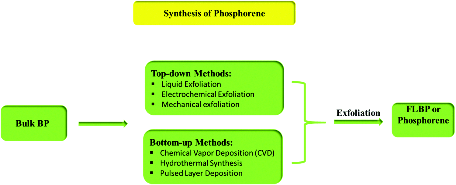 | ||
| Fig. 2 Different preparative methods of FLBP or phosphorene.94 | ||
3.1. Top-down methods
The top-down methods comprise synthetic processes such as liquid-phase exfoliation, mechanical exfoliation, and electrochemical exfoliation.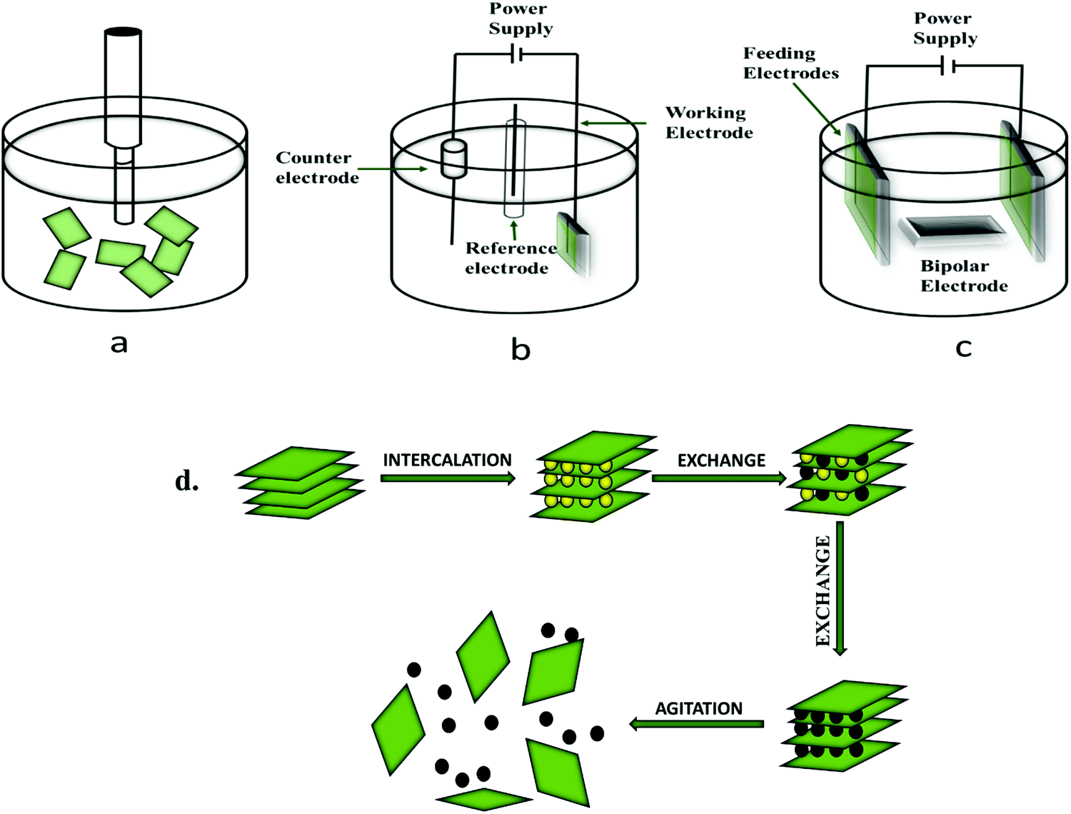 | ||
| Fig. 3 Schematic representation of liquid-based exfoliation, (a) ultra sonication, (b) electrochemical anodic or cathodic method, (c) bipolar electrochemical exfoliation method, and (d) schematic representation showing the exfoliation of BP nanosheets. | ||
The exfoliation of BP via the ultra-sonication method involves dispersion in a preferable solvent followed by sonication, and then the exfoliated nanosheets are collected by the centrifugation method. At the time of sonication, due to the fluctuations and shear forces, micro-and nano-sized bubbles are produced. The solvent molecules, such as N-methyl pyrrolidone (NMP), DMSO, etc., intercalate between the layers of BP and disperse the nanosheets within it, as depicted in Fig. 4. For the liquid-based exfoliation through the ultrasonic method, selection of a favorable liquid solvent system for dispersion and exfoliation is necessary. The theoretical calculations of surface energy and surface tension provided information on the suitability of solvents for the exfoliation of 2-D materials. Previous studies confirmed that with the increase in surface tension of solvents, the exfoliation yield of BP increases. Unlike other 2-D materials, the production and large-scale exfoliation of phosphorene nanosheets should be anhydrous and free of oxygen because of the chemisorption of O-atoms by P-atoms present on the surface of BP nanosheets.95–101
3.1.2.1 Anodic electrochemical exfoliation. It is a simple method and the implementation is also easy. Among all the aqueous electrolytes for anodic exfoliation, sulfates are the most efficient negative ions for such types of exfoliations.108 The first group to use anodic exfoliation to prepare BP nano sheets was Ernade and coworkers using Na2SO4 solution. Their work involves the use of BP and Pt wire as an anode and a counter electrode, respectively.109 Since, their work does not provide any information regarding the nanosheets’ morphology, yield, mechanism, and defects, they further studied and tried to prepare exfoliated BP with a yield of about 80% using an excellent mechanical approach. However, during exfoliation, Ph is prone to oxidation.110 Ambrosi and co-workers evaluated the anodic exfoliation of BP in an acidic solution, i.e., H2SO4, both in the presence and absence of an applied potential (3 V). The main advantage of anodic exfoliation is that it can work at a lower potential, which may lead to the low probability of oxidation of the BP nanosheets.111
3.1.2.2 Cathodic electrochemical exfoliation. This method involves the insertion of electrolytes and positive ions inside the nanosheets of BP by applying a negative potential. Cathodic exfoliation has more efficiency than the anodic one due to the low oxidation rate.112 The used intercalating agent must have high solubility in the solvents to generate cations at high voltage.
Lingxin et al., in their work, forward a highly efficient and simple method to synthesize and exfoliate BP through the electrochemical cathodic exfoliation process using ethylene imine polymer (PEI) as a solvent. This method does not involve any high temperature, pressure, or sonication. PEI, in this context, acts as an expanding agent to expand the layers of BP. This PEI-FLBP composite could prevent the newly peeled-off FLBP from accumulating and improve the compatibility between PEI-FLBP nanosheets and the waterborne polyurethane (WPU) matrix. This FLBP-PEI and WPU matrix has significantly increased the tensile stress.113
He et al. reported a cathodic electrochemical method for the exfoliation of bulky BP into FLBP. In general, the already established method for electrochemical exfoliation in an aqueous solution may result in the oxidation of the BP nanosheets.112 Therefore, their group showed an appropriate and straightforward method that would exfoliate the crystals of BP into nanosheets and reduce the oxidation efficiency.114
3.1.2.3 Electrolytic electrochemical exfoliation. Bulk BP is necessary for anodic and cathodic electrochemical exfoliation. These materials are expensive and can hamper the application of electrochemical exfoliation in preparing the sheets of phosphorene. Baboukani et al. contrive high quality and orthorhombic crystal structured phosphorene through electrochemical exfoliation using deionized water.115 This work does not involve any expensive bulk BP and Pt electrodes or any other organic solvents. This method is cost-effective and environmentally friendly and provides insight into future advances in the electrochemical exfoliation of BP into Ph nanosheets. In 2016, Mayorga-Martinez and co-workers synthesized BP nanoparticles using electrochemical exfoliation in Na2SO4 solution by applying opposite potentials.116
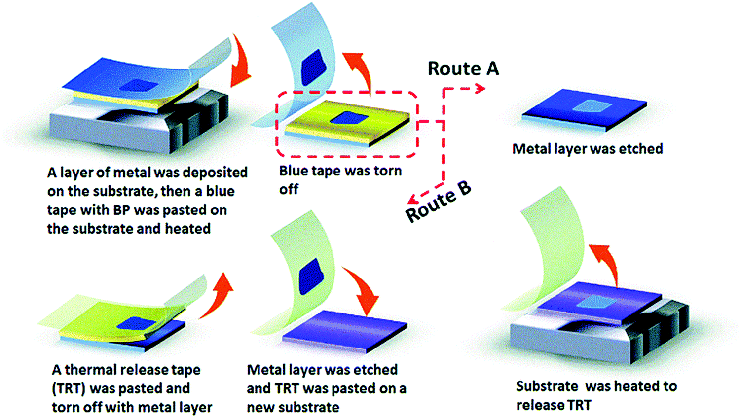
Sha et al., in their paper, found that a fine layer of Au or Ag on the Si/SiO2 substrate can notably enhance the yield and the exfoliation of FLBP.120 In this work, a layer of Ag or Au is first deposited on the surface of Si/SiO2, Si water, or other substrates like PDMS using magnetron sputtering. BP is then pasted on the surface of the blue tap and put on the substrate, followed by heating. The blue tape is ripped off, and to keep the FLBP on the substrate, the metal layer on it to be removed. FLBP can also be transferred onto other preferred solvents using this technique. Fig. 4 shows the diagrammatic depiction of metal-assisted exfoliation of BP.
Commonly used metal-assisted exfoliation has disadvantages such as instability, low yield, and lack of control regarding size, thickness, and shape. To overcome these obstacles and obtain a high yield of nano BP, polydimethylsiloxane (PDMS) can be used as an additional layer on the substrate.122 The transfer of BP via the PDMS substrate using the fully dry transfer technology can solve the problem of adhesive tape residue.123 The metal-assisted mechanical exfoliation method was introduced to synthesize FLBP with a lateral size of >50 μm and a surface area larger than the one obtained from the typical scotch tape technique.124 Although this process shows some positive results, the uncontrollable morphology and low yield of BP still need to be addressed.
3.2. Bottom-up method
Bottom-up methods include chemical vapor deposition (CVD), hydrothermal synthesis, and pulsed layer deposition. It can be said that to date there has been no promising method known for the large-scale synthesis of phosphorene. The main idea to synthesize phosphorene via the bottom-up process came from the approaches usually used for graphene and transition metal di-chalcogenides (TMD). However, CVD helps to grow graphene and monolayers of TMD but is not reliable for phosphorene because suitable non-toxic phosphorus-based precursors are absent. In the hydrothermal synthesis, the main problem is the instability of phosphorene as it is prone to oxidation. One can successfully synthesize phosphorene under oxygen-free conditions using wet chemical methods such as solvothermal synthesis, self-assembly, template-assisted growth; and hydrothermal processes.125Tian et al., in their paper, discussed the synthetic process for FLBP nanosheets in gram-scale quantities through the bottom-up approach. They have used white phosphorus as the raw material, which involves an ethylene diamine system of the direct solvothermal process operating in a temperature range of 60–140 °C, as shown in Fig. 6. The 2-D material has a 0.8–1.0 μm lateral size, where the thickness of flakes decreases with increasing temperature until 100 °C. However, a further increase in the temperature results in an increase in flake thickness. The thickness corresponding to 2–28 phosphorene atomic layers is about 1–15 nm. Even though the occurrence of oxidation was unavoidable in the sample, it was considered as an advantageous synthetic procedure for improving BP stability.126
The synthesis of FLBP via the solvothermal process has been depicted schematically in Fig. 5.
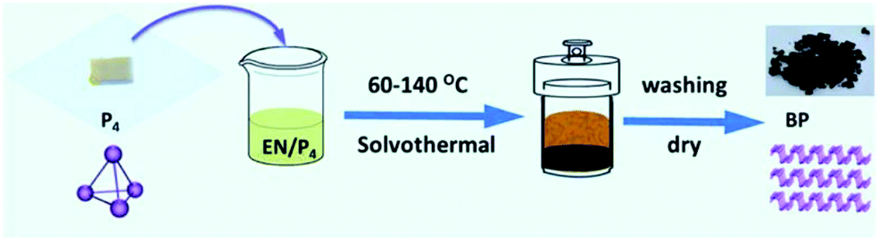 | ||
| Fig. 5 Schematic representation of the synthesis of FLBP via the solvothermal process (reproduced from M. Pica and R. D’Amato, Chemistry of Phosphorene: Synthesis, Functionalization and Biomedical Applications in an Update Review. Inorganics, 2020, 8(4), 29.; published by MDPI, Basel, Switzerland). This article is an open access article distributed under the terms and conditions of the Creative Commons Attribution license (https://doi.org/10.3390/inorganics8040029). | ||
Gao et al. showed that the breaking of phosphorene sheets is initiated due to the strong interaction between phosphorus and the substrate, while the weak interaction is not much effective in stabilizing the 2-D sheets. An intermediate exchange per P-atom of about 0.35 eV is required for the proper growth of 2-D phosphorene. They also studied the effect of divergent substrate growth of phosphorene on Au (111), tellurium functionalized Au (111), and Cu (111). According to their investigation, the interaction of phosphorus with Cu (111) is strong, leading to random dispersion of phosphorus nanoclusters and single atoms. Au (111) functionalized tellurium (Te) can weaken the monolayer interaction between phosphorus and the substrate. The successful growth of a quasi, free-standing single-layer phosphorene on Te/Au (111) was observed with the help of low-temperature scanning tunneling microscopy (LT-STM), X-ray photoelectron spectroscopy (XPS), and density functional theory (DFT). Such successful quasi, free-standing films could further enable their application in fields of optoelectronic and electronic devices.127
There are reports which show the molecular beam epitaxy (MBE) growth of FLBP quantum dots (BPQD) on Si substrate using Pwhite as the precursor at a shallow temperature. According to the AFM analysis, the average radius and height were 27.5 ± 5 nm and 3.1± 0.6 nm, respectively, for BPQDs.128
Recently, the growth mechanism of phosphorene and BP from the gas phase was reported where SnI2 acted as the important gas phase species to activate and transform white phosphorus into phosphorene.129
4. Functionalization of phosphorene
According to their specific applications, the functionalization of 2-D materials is carried out to tune their chemical, physical, and electronic properties. Functionalization of phosphorene is usually aimed at improving stability as it is prone to oxidation when coming into contact with air and oxygen. On exposure to light, the degradation of phosphorene speeds up to form phosphate on the surface. The oxidation rate can be reduced by monitoring the thickness, light intensity, oxygen concentration, and energy gap.130,131 However, the oxidative degradation of phosphorene is under investigation and not well understood yet. There are numerous blueprints to overcome such disadvantages and stabilize phosphorene through functionalization. The stabilization techniques include introducing a thin protection layer to prevent oxidation, lead to the formation of a heterostructure, and organic molecule passivation. Formation of such conjugates takes place via non-covalent interaction, encapsulation, transition metal acceptor fragments, or covering the surface with acidic chemical groups.132 Covalent and non-covalent functionalization could enhance the intrinsic properties and circumvent the deterioration of the electronic structure of phosphorene. For instance, phosphorene can bind with soft materials, forming an advanced functionalized material.133,134Kumar et al., in their work, reported the functionalization of phosphorene with an artificial helical copolymer (a polypeptide). The composition of the biocompatible polypeptide with BP nanosheets could be suitable for biomedical devices for drug delivery and sensors. The main advantages of using such materials include (i) the passivation and encapsulation of BP nanosheets, (ii) their electronic interaction with BP nanosheets, (iii) the fabrication of BP in devices without sacrificing their inherent properties, and (iv) the protection of BP nanosheets from atmospheric oxygen.133
In another study, Pumera et al. reported the functionalization of BPSE (shear exfoliated BP) using non-covalent anthraquinone (AQ). In this process, BP and AQ were first exfoliated and then suspended in methanol, leading to the formation of a carbon-based layer in the BPSE-AQ sample with a lower oxidation rate which can be proven by XPS.134
Toffanin et al. studied the nature of physical and chemical interactions between 2-D BP and boronic acid or ester derivatives of pyrene. They showed the stability of 2-D BP on all the derivatives of boronic functionalities. This interaction leads to the limiting of the bandgap by around 0.10 eV of 2-D BP. According to them, modification of electronic structures can also increase the stability of such adduct. Such stabilizing interactions of 2-D BP and the conjugated organic molecules can be helpful in the synthesis of heterojunctions for optoelectronics, photonics, and chemical sensing applications.135
Wu et al. showed in their studies that the self-assembled monolayers of phosphorene with hexamethylenediamine (HMA) in chloroform encapsulated the surface of the material. First, a glove box was rigged to have definite oxygen and water levels, which would result in uniform hydroxylation. The introduction of – OH groups promotes the interaction with amino groups of HMA via hydrogen or ionic bonds to acquire a homogenous protective monolayer with a thickness of ∼ 1.4 nm.136
Hair et al. developed a three-dimensional aptasensor for detecting norovirus using a BP–gold nanoparticle composite (BP–AuNCs). This composite has been prepared by in situ reduction of BP nanosheets with chloroauric acid. They have designed a movable working electrode that increases the ease of sampling and surface area and minimizes cross-contamination. The proposed aptasensor exhibits high selectivity, stability, and repeatability. This 3D aptasensor may provide a cost-effective, facile prototype for the detection of norovirus.137
Yanting and co-workers reported a new material for sensing based on phosphorene and a 2-D triazine polymer. These polymer sheets can prevent the opaque assemble of gas molecules on the surface of phosphorene, leading to a profuse pathway for the penetration and adsorption of gas molecules. Such nanocomposite evinces ambient selectivity, sensitivity, flexibility, and stability to detect gases like NO2. This nanospacer intercalation blueprint can enlarge the 2-D nanomaterials for gas sensing. This outcome provides an ingenuity to improve more such 2-D polymer and nanomaterial composites for wearable electronics.138
5. Superiority over graphene and other 2-D materials
Following the discovery of graphene in 2004, 2-D materials have emerged as potential candidates in materials science and technology. 2-D materials, such as graphene, MoS2, TMDs, etc., have found applications in photovoltaics, photodetectors, and light emitters. Although graphene and other 2-D materials exhibit some excellent properties, their applications have been limited due to their large bandgap, resulting in optical absorptivity shrink. In addition, structural modification of these materials also could not tune their bandgap, and therefore a substitute to the existing 2-D materials was necessary.The discovery of BP led to the foundation stone for developing materials with appreciable and tunable bandgaps, which was the primary concern towards using 2-D materials. Thus BP can be considered as one of the potential material for a wide range of areas including energy production and storage among the other 2-D materials. Although the bulk form was successfully synthesized about 100 years ago, its 2-D form was demonstrated only in 2014 by the mechanical exfoliation method. BP is a semiconductor with a direct bandgap in bulk and monolayer forms of about ∼0.3 eV and ∼2 eV, respectively, thereby bridging the gap between other 2-D semiconducting materials (TMDs ∼ 1.29 eV to ∼1.8 eV) and graphene (0 eV). The tunable bandgap of BP has made it a potential candidate for developing transistors, photodetectors, sensors, optical devices, solar cells, catalysts, thermoelectrics, triboelectric nanogenerators, supercapacitors, and batteries and in bioimaging. Although it has some fascinating properties which originated from its unique structural features, some intrinsic deficiencies are also observed. Several methods could resolve the inherent flaws, including surface passivation, deposition of protective layers, and surface functionalization by chemical passivation for better stabilization and performance. Nevertheless, BP is currently the best material of choice for these wide range of applications.139–170
6. Application
Black phosphorus, a blueprint of phosphorene, has been known for more than 100 years. It is a candidate for various applications, including electronics, energy, photothermal devices, sensing, optoelectronics, photovoltaics, and batteries, demonstrated in multiple aspects.171 The schematic representations showing various applications of phosphorene are depicted in Fig. 6.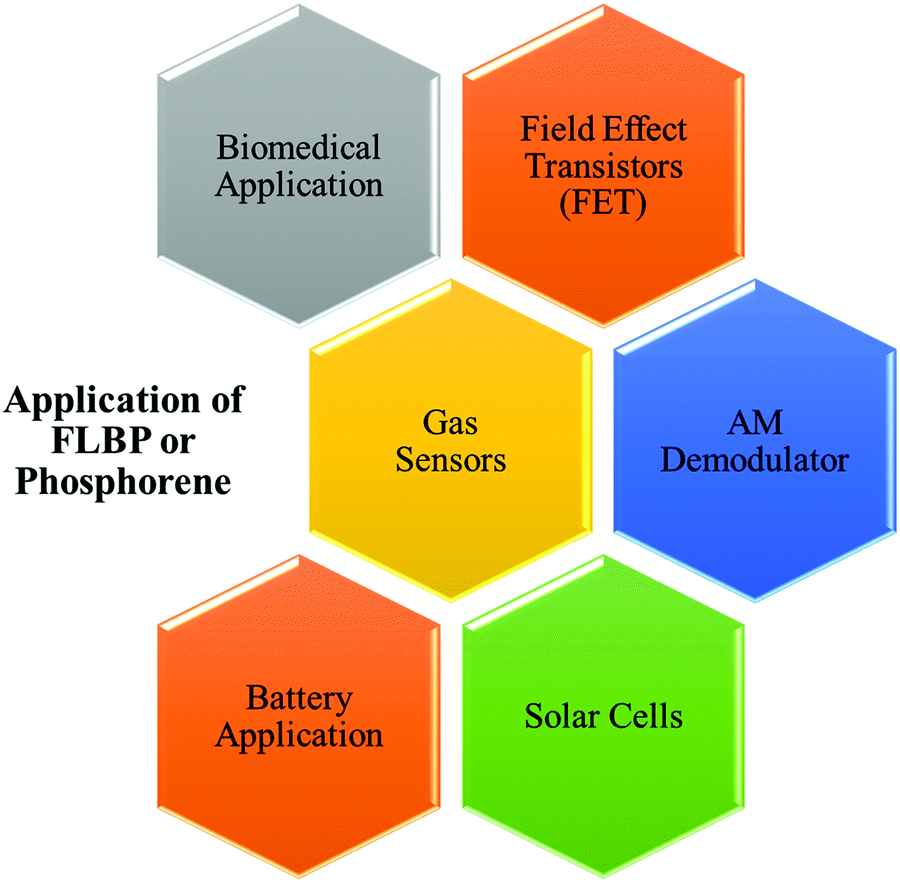 | ||
| Fig. 6 Different applications of FLBP or phosphorene. | ||
6.1. BP for solar cells
The complete replacement of fossil fuels and nuclear energy has been a crucial issue in modern society and for the future. A genuinely sustainable alternative for such energy sources should be cheap, renewable, clean, and safe.172 The radiation of the sun can be harnessed in all areas of the world; this idea has received considerable attention. Solar energy can be used to generate electricity (photovoltaics, PV) or for heating. However, the cost-effectiveness and low sunlight-to-electrical energy efficiency limit their applicability, and hence the replacement of Si solar cells is necessary.In recent years, scientists have mainly focused on developing semiconducting materials, organic compounds, dye sensitizers, perovskite crystals, heterojunction interfaces, and quantum dots (QDs), which are cost-effective and exhibit high performance compared to Si solar cells.173 Intriguingly, BP has a stellar set of properties that qualify it for application in solar cells, namely, carrier mobility, high ambipolar transport properties, and tunable bandgap.174,175 BP and its derivatives have the potential to be used in developing high efficiency solar cells based on the grounds of theoretical and experimental results. Zhang et al. reported a perovskite solar cell with high efficacy and stability. Thoughtful design and positioning of BP with tailored thickness as dual-functional nanomaterials enhance the carrier extraction at the perovskite/hole transport layer and electron transport layer/perovskite interface for highly stable and efficient perovskite solar cells. The combination of appreciative sequencing and collective cascade interfacial carrier extraction, rendered by concurrent positioning of BP, delivered a progressively enhanced power conversion efficiency from 16.95% to 19.83%. Further investigation revealed that BP incorporation through light absorption and reduced trap density can improve the performance of photovoltaic systems. This results in the pleading characteristics of the astute contrivance of BP as a dual-functional transport material for various sensors, light-emitting diodes, photodetectors, optoelectronic devices, etc.176
Zhiheng and co-workers developed a new phosphorene–polyimide and polyethylene glycol (PEG) aerogel composite to amplify the photo thermal energy. This aerogel composite leads to a remarkable increase in photo thermal energy and solar light absorption. The loading of PEG increases the volume capacity of the hybrid aerogel, obtained from the inception of Ph nanosheets. The hybrid polyimide–phosphorene and PEG exhibit photo thermal efficiency and latent heat capacity of 82.5% and 170 J g−1 respectively. This performance makes this hybrid composite effective for a broad range of solar energy storage and capture. This study also provides some encouraging blueprint for the development and design of high-performance hybrid materials for efficient utilization in the field of solar energy.177
Prabhat et al. investigated the effect of adsorption of atoms like K and Li based on the optical properties of BP using density functional theory (DFT). Their study reveals an enhancement of absorption of light for K and Li- atoms adsorbed on phosphorene in the visible range. Calculations suggested a negligible bandgap in the adsorbed structure than the pristine phosphorene. The peaks observed for the refractive index and dielectric constant are in accordance with the peaks in absorption. This high adsorption in the visible region suggested application in optoelectronic devices, including solar cells.178
Jian et al. in their work crossed linked BP and a hexagonal boron nitride graphene hybrid material rationally and calculated the high-power conversion efficiency of about 21.3% for excitonic solar cells (XSC). This heterojunction's excellent photo electronic conversion performance is due to the small conduction band offset, suitable bandgap (1.41 eV), and good visible light response. The boron nitride-graphene substrate with uneven interlayer charge transfer results in hole–electron puddle formation at the interfaces of the heterojunction. This will lead to a prototype of an optoelectronic device, which may be considered as a new direction for developing electronic energy storage devices in the near future.179
6.2. BP for biomedical application
Owing to the exceptional properties of 2-D materials, they have attracted a spectacular status in various technological and scientific disciplines. Compared to other 2-D materials, phosphorene or monolayer of BP has fascinating properties like excellent ON–OFF ratio, tunable bandgap, good carrier mobility, non-toxic biodegradability, and potent in vivo biocompatibility. For future biomedical technology, it is also a promising material. However, the practical approach is still highly challenging. Proper characterization and functionalization can make phosphorene a valuable material for future theranostic and biomedicine scenarios, regardless of such difficulties. However, 2-D materials like BP, MoS2, graphene, hBN, WSe2, etc. exhibit good biocompatibility based on the size of the material and concentration. When compared to other 2D materials, BP exhibits less cytotoxicity. Therefore, it is ideal for biomedical applications such as cancer therapy, biosensors, imaging and photothermal therapy, photoacoustic applications, drug delivery, photodynamic therapy, neural recognition, 3-D printing scaffold, etc. As it is a new material, there must be a proper investigation regarding the various inflammatory responses inside the systems and its effect on environmental exposure and reducing toxicity.180BP is readily biodegradable inside the human body, producing non-toxic intermediates such as phosphates, phosphites, etc. It makes BP a suitable material for different in vivo biomedical applications.181 However, other materials may accumulate inside the system, contributing to cytotoxicity and thus require essential functionalization with various surface coatings. It has both electron transferring and electron-donating capacities; combining these can enhance the reducibility of a catalyst in a reaction, improving biosensors’ sensitivity. Therefore, easy degradation and stability-related issues become an advantage in biosensor applications. This advantage paved the way to enhance catalytic activity and possibility of constructing colorimetric biosensors for the first time. This work was performed using a hybrid BP–Au, synthesized by mixing FL-BP and Au precursor for about a few minutes at room temperature.182 BP also has ambipolar nature, helpful for detecting positively and negatively charged species, making it suitable for biosensing applications. The non-toxic biodegradability of BP makes it ideal for cancer therapy. It can also be used for detecting various bio analytes (e.g., immunoglobin (IgG) and myoglobin (Mb)) due to its tunable bandgap.183
Shabeer et al., theoretically showed the ability of a carrier for thioguanine in drug delivery to treat diseases like cancer. Thioguanine is used for the treatment of leukemia. However, it is not biocompatible and has low aqueous solubility limiting its performance in cancer treatment. On the Ph surface, they have found three stable configurations of thioguanine with the absorption energy ranging from −76.99 kJ mol−1 to −38.69 kJ mol−1, indicating physisorption of the drug on the phosphorene surface.184
6.3. Field effect transistors (FETs)
After the successful fabrication of FET using phosphorene in 2014 by Brien et al. and other groups, there have been many significant developments that have showcased phosphorene's novel properties for a variety of fields. These include engineering of electronic properties by strain, intrinsic electronic and transport properties, electric field, or doping of a transition metal; new phosphorene polymorphs with negligible molecular adsorption; gas sensors; low dimensional phosphorene derivatives; devices in electronics; and in photovoltaics.185–210 Among all the applications of phosphorene, the most notable one is the fabrication of FETs. Conduction channels of a phosphorene-based FET can track the permitted light with different wavelengths. Therefore, it is a highly preferred material for near IR and night-vision imaging applications. Thus, researchers are making efforts to accomplish the performance of BP to construct PN junctions and solar cells.For transistor applications, digital electronics takes huge advantage of the potential of semiconductors. The main criteria for achieving a great ON/OFF ratio are excellent charge mobility and adequate bandgap for high conductivity, low power consumption, and operational switching. In such cases, 2-D materials, especially phosphorene, with a controllable bandgap of 0.32 eV exhibited inclusive properties as a prospective transistor material. At room temperature, phosphorene has a high charge carrier mobility of about 600 cm2 V−1 S−1, leading to rationally rapid operation. The ability to tune the bandgap is notably valuable for electronic applications, specifically FETs. Due to adequate carrier mobility, it finds its uses in high voltage application with power gain. Phosphorene-based devices can be useful in high-frequency electronics because of their excellent current saturation properties. Thus, it is considered a prospective material for high-performance thin-film electronics applications at higher frequency. As phosphorene has a favorable bandgap and excellent mobility, it can also be used beyond transistors. It is used in semiconductor electronics, i.e., amplitude modulated (AM) demodulators and circuits active for loudspeakers and radio receivers.211
6.4. Gas sensors
Among all the fascinating properties, the exceptional in-plane anisotropy of phosphorene influences its electrical, optical, mechanical, transport, and thermoelectric properties.Liangzhi et al. calculated the adsorption of gas molecules like NO2, CO2, NO, CO, and NH3 on the monolayer surface of phosphorene. According to their result, phosphorene's sensing performance transcends that of other 2D materials. They have determined the optimal adsorption of such gas molecules on the phosphorene surface, identified the molecular doping, and calculated the I–V relation using NEGF (non-equilibrium green's function formalism).212
Although there are numerous theoretical studies on phosphorene-based chemical sensors, a few experimental verifications are there for the introductory studies of this material. Ahmed et al. reported a chemical sensor using field-effect transistors based on BP. This BP-based gas sensor can detect NO2 down to 5 ppb and is very sensitive. Its conductivity changes upon exposure to 5, 10, 15, 20, and 40 ppb, followed by the Langmuir isotherm for the adsorption on the surface. These results give an idea on the sensing and electronic characteristics of BP, which can be of great importance in near future.16 It is a material of choice and can easily replace current MoS2 and graphene gas sensor materials. Far-reaching research has been performed to study the adsorption of gases like CO, CO2, NH3, and NO on single layers of graphene, MoS2, and phosphorene. Among these materials, phosphorene shows better physisorption towards all the gaseous molecules due to its controllable electronic properties in optoelectronics and switching devices. Thus, it is one of the most suitable single-electron transistors (SET) for gas sensing applications. There are some reports regarding highly sensitive recognition of N-based molecules because of the stronger doping of phosphorene.213,214
Dian et al., in their work, substituted the P-atom of BP using Pt, Ag, and Au as dopants, which are more stable than the BP with only one substituted P-atom. They have shown the use of Ag-2P and Au-2P to detect NO gas. These dopants showed better catalytic activity toward the hydrogen evolution reaction than intact BP.215
6.5. Battery application
2D materials grab significant attention as anode materials in battery application due to their outstanding electronic properties and excellent surface-to-volume ratio. Current investigation and theoretical research have disclosed that phosphorene, with a high theoretical specific capacity of 2596 mA h g−1 and a potential of 0.4–1.2 V, can be a promising material for battery application. However, as an electrode, due to its good electrical conductivity, it possesses the potential to be used in rechargeable battery application in many industrial fields. At a 0.2 C current rate, the discharge capacity of phosphorene outperforms that of graphene by a factor of 7, which is higher than that of Li-ion batteries based on graphite, Ge, and Sn as anode materials. The reliability is demonstrated with a cycling life test, and it appears that the capacity retention of phosphorene after 100 cycles is 80%.216There has been an extensive development of phosphorene-based Li-ion batteries as they have a reversible capacity and excellent cyclic continuance. The activity of such a battery is highly dependent on the capacity of Li and the cycling rate of anode materials. It has been confirmed that the binding of Li atoms with single-layered phosphorene is more robust than that with the bi-layered one. Therefore, monolayer phosphorene is appropriate as an anode material in Li-ion batteries, exhibiting larger capacity and lower open-circuit voltage. Calculations involving the ability of single-layer phosphorene show that it is superior as compared to other commercialized materials, which include graphite (372 mA h g−1), TiO2 polymorphs (200 mA h g−1), and Ti3C2 (320 mA h g−1).217–219
6.6. Amplitude-modulated (AM) demodulators
Amplitude-modulated (AM) demodulators are based on flexible BP, introduced recently to radio receivers, consisting of a single ambipolar BP transistor. The promoted mechanical robustness of BP transistors for uniaxial tensile strain and bending cycles is up to 2% and 5000, respectively. The fabrication method of flexible BP transistors on polyimide exhibited the most significant device mobility of almost 310 cm2 V−1 s−1, superior to the maximum TMD transistors’ mobility. A study of BP-based AM modulator disclosed that it is the most appropriate layered semiconductor in terms of flexible nanoelectronics because of its remarkable properties, like ambipolar transport, excellent current saturation, and high mobility in an ambient environment.2207. Conclusions and future prospects
The present review thoroughly explores the preparation, properties, functionalization, and applications of BP, FLBP or phosphorene in various fields. Due to their unique properties, phosphorene and its derivatives can be advanced materials for different applications in different areas, including electrical, energy storage, and optical applications. However, phosphorene is at the very early stage of development and has some issues which need to be resolved before its widespread practical application. As a relatively new member of the 2-D family, it displays exceptional properties over other materials like graphene and TMDCs. It combines a very desirable tunable bandgap with high charge mobility, which is indispensable for the recently demonstrated excellent performance of phosphorene-based devices such as the FETs. Extensive theoretical and experimental investigations have shown that phosphorene's novel electronic, mechanical, and transport properties exhibit intrinsic anisotropic behavior. Their electronic and transport properties are increasingly being investigated and understood, resulting in new opportunities for development and future research activities. Such unique characteristics make phosphorene an intriguing material among the burgeoning families of 2-D layered materials with significant applications in electronics and photovoltaics. Currently, most researchers focus on phosphorene's application and device demonstrations based on its tunable bandgap and high electron mobility.Further work in phosphorene functionalization may reveal some superior properties and performance and other possible adjustments. However, challenges and opportunities coexist in studying and utilizing new materials. Degradation of phosphorene by oxidation and hydrophilicity are the significant hurdles that must be overcome for advanced future applications. Encapsulation and surface passivation techniques are some practical strategies that can ensure or even reduce structural and property degradation. Overall, its unique properties make it a promising material in materials science. The design and fabrication of advanced nanodevices and more fundamental and technological breakthroughs can be expected soon.
Conflicts of interest
There are no conflicts to declare.Acknowledgements
The authors would like to thank the Department of Science and Technology, Government of India, for funding this work. N. Sultana would like to thank DST for providing INSPIRE fellowship (IF190428). A. Degg thanks the TUM Graduate School and the IRTG 2020 Alberta/Technical University of Munich International Graduate School (ATUMS) for continuous support. The authors would also like to thank Gautomi Gogoi, Bandita Kalita, Kangkan J Goswami, and Hridoy Jyoti Bora for their valuable suggestions.References
- M. Qiu, W. X. Ren, T. Jeong, M. Won, G. Y. Park, D. K. Sang and J. S. Kim, Omnipotent phosphorene: a next-generation, two-dimensional nanoplatforms for multidisciplinary biomedical applications, Chem. Soc. Rev., 2018, 47(15), 5588–5601 RSC.
- A. E. Rezaee, M. A. Kashi and A. Baktash, Stone-Wales like defects formation, stability, and reactivity in black phosphorene, Mater. Sci. Eng., B, 2018, 236, 208–216 CrossRef.
- M. Batmunkh, M. Bat-Erdene and J. G. Shapter, Phosphorene and phosphorene-based materials–prospects for future applications, Adv. Mater., 2016, 28(39), 8586–8617 CrossRef CAS.
- L. Kou, C. Chen and S. C. Smith, Phosphorene: fabrication, properties, and applications, J. Phys. Chem. Lett., 2015, 6(14), 2794–2805 CrossRef CAS PubMed.
- S. Bagheri, N. Mansouri and E. Aghaie, Phosphorene: a new competitor for graphene, Int. J. Hydrogen Energy, 2016, 41(7), 4085–4095 CrossRef CAS.
- M. Batmunkh, M. Bat-Erdene and J. G. Shapter, Phosphorene and phosphorene-based materials–prospects for future applications, Adv. Mater., 2016, 28(39), 8586–8617 CrossRef CAS PubMed.
- H. Liu, A. T. Neal, Z. Zhu, Z. Luo, X. Xu, D. Tománek and P. D. Ye, Phosphorene: an unexplored 2D semiconductor with a high hole mobility, ACS Nano, 2014, 8(4), 4033–4041 CrossRef CAS PubMed.
- S. Balendhran, S. Walia, H. Nili, S. Sriram and M. Bhaskaran, Elemental analogues of graphene: silicene, germanene, stanene, and phosphorene, Small, 2015, 11(6), 640–652 CrossRef CAS PubMed.
- J. B. Smith, D. Hagaman and H. F. Ji, Growth of 2D black phosphorus film from chemical vapor deposition, Nanotechnology, 2016, 27(21), 215602 CrossRef PubMed.
- A. Chaves, W. Ji, J. Maassen, T. Dumitrica and T. Low, Theoretical overview of black phosphorus, arXiv preprint arXiv:1710.05808, 2017.
- Y. Xu, Z. Shi, X. Shi, K. Zhang and H. Zhang, Recent progress in black phosphorus and black-phosphorus-analogue materials: properties, synthesis and applications, Nanoscale, 2019, 11(31), 14491–14527 RSC.
- A. Carvalho, M. Wang, X. Zhu, A. S. Rodin, H. Su and A. H. C. Neto, Phosphorene: from theory to applications, Nat. Rev. Mater., 2016, 1(11), 1–16 Search PubMed.
- V. Sorkin, Y. Cai, Z. Ong, G. Zhang and Y. W. Zhang, Recent advances in the study of phosphorene and its nanostructures, Crit. Rev. Solid State Mater. Sci., 2017, 42(1), 1–82 CrossRef CAS.
- Y. Cai, G. Zhang and Y. W. Zhang, Structure, Phonons, and Defects. Phosphorene: Physical Properties, Synthesis, and Fabrication, 2019 Search PubMed.
- A. Goswami and M. B. Gawande, Phosphorene: Current status, challenges and opportunities, Front. Chem. Sci. Eng., 2019, 13(2), 296–309 CrossRef.
- A. N. Abbas, B. Liu, L. Chen, Y. Ma, S. Cong, N. Aroonyadet and C. Zhou, Black phosphorus gas sensors, ACS Nano, 2015, 9(5), 5618–5624 CrossRef CAS PubMed.
- Y. Ma, C. Shen, A. Zhang, L. Chen, Y. Liu, J. Chen and C. Zhou, Black phosphorus field-effect transistors with work function tunable contacts, ACS Nano, 2017, 11(7), 7126–7133 CrossRef CAS PubMed.
- M. Qiu, W. X. Ren, T. Jeong, M. Won, G. Y. Park, D. K. Sang and J. S. Kim, Omnipotent phosphorene: a next-generation, two-dimensional nanoplatform for multidisciplinary biomedical applications, Chem. Soc. Rev., 2018, 47(15), 5588–5601 RSC.
- J. R. Choi, K. W. Yong, J. Y. Choi, A. Nilghaz, Y. Lin, J. Xu and X. Lu, Black phosphorus and its biomedical applications, Theranostics, 2018, 8(4), 1005 CrossRef CAS PubMed.
- W. Zhang, Y. Chen, T. Huynh, Y. Yang, X. Yang and R. Zhou, Directional extraction and penetration of phosphorene nanosheets to cell membranes, Nanoscale, 2020, 12(4), 2810–2819 RSC.
- S. Chakravarty, B. Gogoi, B. B. Mandal, N. Bhardwaj and N. S. Sarma, Silk fibroin as a platform for dual sensing of vitamin B12 using photoluminescence and electrical techniques, Biosens. Bioelectron., 2018, 112, 18–22 CrossRef CAS.
- S. Dharani, V. Nagarajan and R. Chandiramouli, Perceptions on the adsorption of COPD biomarker vapors on violet phosphorene nanosheet-A first-principles study, J. Mol. Graphics Modell., 2019, 91, 22–29 CrossRef CAS PubMed.
- H. Zhang, Ultrathin two-dimensional nanomaterials, ACS Nano, 2015, 9(10), 9451–9469 CrossRef CAS PubMed.
- L. Niu, J. N. Coleman, H. Zhang, H. Shin, M. Chhowalla and Z. Zheng, Production of two-dimensional nanomaterials via liquid-based direct exfoliation, Small, 2016, 12(3), 272–293 CrossRef CAS PubMed.
- L. Kou, C. Chen and S. C. Smith, Phosphorene: fabrication, properties, and applications, J. Phys. Chem. Lett., 2015, 6(14), 2794–2805 CrossRef CAS PubMed.
- M. Z. Rahman, C. W. Kwong, K. Davey and S. Z. Qiao, 2D phosphorene as a water splitting photocatalyst: fundamentals to applications, Energy Environ. Sci., 2016, 9(3), 709–728 RSC.
- H. Liu, Y. Du, Y. Deng and D. Y. Peide, Semiconducting black phosphorus: synthesis, transport properties and electronic applications, Chem. Soc. Rev., 2015, 44(9), 2732–2743 RSC.
- Y. Jing, X. Zhang and Z. Zhou, Wiley Interdiscip. Rev.: Comput. Mol. Sci., 2016, 6, 5 CAS.
- T. Nilges, P. Schmidt and R. Weihrich, Phosphorus: the allotropes, stability, synthesis, and selected applications, Encycl. Inorg. Bioinorg. Chem., 2011, 1–18 Search PubMed.
- R. Hultgren, N. S. Gingrich and B. E. Warren, The atomic distribution in red and black phosphorus and the crystal structure of black phosphorus, J. Chem. Phys., 1935, 3(6), 351–355 CrossRef CAS.
- R. W. Keyes, The electrical properties of black phosphorus, Phys. Rev., 1953, 92(3), 580 CrossRef.
- S. Endo, Y. Akahama, S. I. Terada and S. I. Narita, Growth of large single crystals of black phosphorus under high pressure, Jpn. J. Appl. Phys., 1982, 21(8A), L482 CrossRef CAS.
- S. Lange, P. Schmidt and T. Nilges, Au3SnP7@black phosphorus: an easy access to black phosphorus, Inorg. Chem., 2007, 46(10), 4028–4035 CrossRef CAS PubMed.
- M. Köpf, N. Eckstein, D. Pfister, C. Grotz, I. Krüger, M. Greiwe and T. Nilges, Access and in situ growth of phosphorene-precursor black phosphorus, J. Cryst. Growth, 2014, 405, 6–10 CrossRef.
- R. Fei, A. Faghaninia, R. Soklaski, J. A. Yan, C. Lo and L. Yang, Enhanced thermoelectric efficiency via orthogonal electrical and thermal conductances in phosphorene, Nano Lett., 2014, 14(11), 6393–6399 CrossRef CAS PubMed.
- H. Y. Lv, W. J. Lu, D. F. Shao and Y. P. Sun, Large thermoelectric power factors in black phosphorus and phosphorene, arXiv preprint arXiv:1404.5171, 2014.
- D. F. Shao, W. J. Lu, H. Y. Lv and Y. P. Sun, Electron-doped phosphorene: a potential monolayer superconductor, EPL, 2014, 108(6), 67004 CrossRef.
- Q. Wei and X. Peng, Superior mechanical flexibility of phosphorene and few-layer black phosphorus, Appl. Phys. Lett., 2014, 104(25), 251915 CrossRef.
- R. Fei and L. Yang, Strain-engineering the anisotropic electrical conductance of few-layer black phosphorus, Nano Lett., 2014, 14(5), 2884–2889 CrossRef CAS PubMed.
- Q. Wu, L. Shen, M. Yang, Z. Huang and Y. P. Feng, Electronic and Transport Property of Phosphorene Nanoribbon. arXiv preprint arXiv:1405.3077, 2014.
- X. Ren, P. Lian, D. Xie, Y. Yang, Y. Mei, X. Huang and X. Yin, Properties, preparation and application of black phosphorus/phosphorene for energy storage: a review, J. Mater. Sci., 2017, 52(17), 10364–10386 CrossRef CAS.
- H. Liu, A. T. Neal, Z. Zhu, Z. Luo, X. Xu, D. Tománek and P. D. Ye, Phosphorene: an unexplored 2D semiconductor with a high hole mobility, ACS Nano, 2014, 8(4), 4033–4041 CrossRef CAS PubMed.
- L. Kou, C. Chen and S. C. Smith, Phosphorene: fabrication, properties, and applications, J. Phys. Chem. Lett., 2015, 6(14), 2794–2805 CrossRef CAS PubMed.
- J. Qiao, X. Kong, Z. X. Hu, F. Yang and W. Ji, High-mobility transport anisotropy and linear dichroism in few-layer black phosphorus, Nat. Commun., 2014, 5(1), 1–7 Search PubMed.
- R. J. Wu, M. Topsakal, T. Low, M. C. Robbins, N. Haratipour, J. S. Jeong and K. A. Mkhoyan, Atomic and electronic structure of exfoliated black phosphorus, J. Vac. Sci. Technol., A, 2015, 33(6), 060604 CrossRef.
- Z. X. Hu, X. Kong, J. Qiao, B. Normand and W. Ji, Interlayer electronic hybridization leads to exceptional thickness-dependent vibrational properties in few-layer black phosphorus, Nanoscale, 2016, 8(5), 2740–2750 RSC.
- A. Rabiei Baboukani, I. Khakpour, V. Drozd and C. Wang, Liquid-Based Exfoliation of Black Phosphorus into Phosphorene and Its Application for Energy Storage Devices, Small Struct., 2021, 2(5), 2000148 CrossRef CAS.
- Y. Esfahani Monfared, Overview of recent advances in the design of plasmonic fiber-optic biosensors, Biosensors, 2020, 10(7), 77 CrossRef PubMed.
- A. Chaves, J. G. Azadani, H. Alsalman, D. R. da Costa, R. Frisenda, A. J. Chaves and T. Low, Bandgap engineering of two-dimensional semiconductor materials, npj 2D Mater. Appl., 2020, 4(1), 1–21 CrossRef.
- H. Fu, Z. Li, H. Xie, Z. Sun, B. Wang, H. Huang and X. F. Yu, Different-sized black phosphorus nanosheets with good cytocompatibility and high photothermal performance, RSC Adv., 2017, 7(24), 14618–14624 RSC.
- L. Li, Y. Yu, G. J. Ye, Q. Ge, X. Ou, H. Wu and Y. Zhang, Black phosphorus field-effect transistors, Nat. Nanotechnol., 2014, 9(5), 372–377 CrossRef CAS PubMed.
- L. Kou, C. Chen and S. C. Smith, Phosphorene: fabrication, properties, and applications, J. Phys. Chem. Lett., 2015, 6(14), 2794–2805 CrossRef CAS PubMed.
- F. Xia, H. Wang and Y. Jia, Rediscovering black phosphorus as an anisotropic layered material for optoelectronics and electronics, Nat. Commun., 2014, 5(1), 1–6 Search PubMed.
- R. Fei, A. Faghaninia, R. Soklaski, J. A. Yan, C. Lo and L. Yang, Enhanced thermoelectric efficiency via orthogonal electrical and thermal conductances in phosphorene, Nano Lett., 2014, 14(11), 6393–6399 CrossRef CAS PubMed.
- R. Fei and L. Yang, Strain-engineering the anisotropic electrical conductance of few-layer black phosphorus, Nano Lett., 2014, 14(5), 2884–2889 CrossRef CAS PubMed.
- A. Jain and A. J. McGaughey, Strongly anisotropic in-plane thermal transport in single-layer black phosphorene, Sci. Rep., 2015, 5(1), 1–5 Search PubMed.
- Q. Wei and X. Peng, Superior mechanical flexibility of phosphorene and few-layer black phosphorus, Appl. Phys. Lett., 2014, 104(25), 251915 CrossRef.
- D. Akinwande, N. Petrone and J. Hone, Two-dimensional flexible nanoelectronics, Nat. Commun., 2014, 5(1), 1–12 Search PubMed.
- F. Bonaccorso, Z. Sun, T. Hasan and A. C. Ferrari, Graphene photonics and optoelectronics, Nat. Photonics, 2010, 4(9), 611–622 CrossRef CAS.
- A. A. Balandin, Thermal properties of graphene and nanostructured carbon materials, Nat. Mater., 2011, 10(8), 569–581 CrossRef CAS PubMed.
- A. Das, S. Pisana, B. Chakraborty, S. Piscanec, S. K. Saha, U. V. Waghmare and A. K. Sood, Monitoring dopants by Raman scattering in an electrochemically top-gated graphene transistor, Nat. Nanotechnol., 2008, 3(4), 210–215 CrossRef CAS PubMed.
- K. I. Bolotin, K. J. Sikes, Z. Jiang, M. Klima, G. Fudenberg, J. Hone and H. L. Stormer, Ultrahigh electron mobility in suspended graphene, Solid State Commun., 2008, 146(9–10), 351–355 CrossRef CAS.
- X. Wei, B. Fragneaud, C. A. Marianetti and J. W. Kysar, Nonlinear elastic behavior of graphene: Ab initio calculations to continuum description, Phys. Rev. B: Condens. Matter Mater. Phys., 2009, 80(20), 205407 CrossRef.
- C. Lee, X. Wei, J. W. Kysar and J. Hone, Measurement of the elastic properties and intrinsic strength of monolayer graphene, Science, 2008, 321(5887), 385–388 CrossRef CAS PubMed.
- Q. H. Wang, K. Kalantar-Zadeh, A. Kis, J. N. Coleman and M. S. Strano, Electronics and optoelectronics of two-dimensional transition metal dichalcogenides, Nat. Nanotechnol., 2012, 7(11), 699–712 CrossRef CAS PubMed.
- W. Huang, H. Da and G. Liang, Thermoelectric performance of mx2 (m = mo, w; x = s, se) monolayers, J. Appl. Phys., 2013, 113(10), 104304 CrossRef.
- S. Sahoo, A. P. Gaur, M. Ahmadi, M. J. F. Guinel and R. S. Katiyar, Temperature-dependent Raman studies and thermal conductivity of few-layer MoS2, J. Phys. Chem. C, 2013, 117(17), 9042–9047 CrossRef CAS.
- H. Peelaers and C. G. Van de Walle, Effects of strain on band structure and effective masses in MoS2, Phys. Rev. B: Condens. Matter Mater. Phys., 2012, 86(24), 241401 CrossRef.
- T. Li, Ideal strength and phonon instability in single-layer MoS2, Phys. Rev. B: Condens. Matter Mater. Phys., 2012, 85(23), 235407 CrossRef.
- M. Abraham and S. E. Mohney, Annealed Ag contacts to MoS2 field-effect transistors, J. Appl. Phys., 2017, 122(11), 115306 CrossRef.
- N. R. Pradhan, D. Rhodes, S. Memaran, J. M. Poumirol, D. Smirnov, S. Talapatra and L. Balicas, Hall and field-effect mobilities in few layered p-WSe2 field-effect transistors, Sci. Rep., 2015, 5(1), 1–8 Search PubMed.
- M. Tosun, S. Chuang, H. Fang, A. B. Sachid, M. Hettick, Y. Lin and A. Javey, High-gain inverters based on WSe2 complementary field-effect transistors, ACS Nano, 2014, 8(5), 4948–4953 CrossRef CAS PubMed.
- W. Liu, J. Kang, D. Sarkar, Y. Khatami, D. Jena and K. Banerjee, Role of metal contacts in designing high-performance monolayer n-type WSe2 field effect transistors, Nano Lett., 2013, 13(5), 1983–1990 CrossRef CAS PubMed.
- H. Fang, S. Chuang, T. C. Chang, K. Takei, T. Takahashi and A. Javey, High-performance single layered WSe2 p-FETs with chemically doped contacts, Nano Lett., 2012, 12(7), 3788–3792 CrossRef CAS PubMed.
- R. Zhang, V. Koutsos and R. Cheung, Elastic properties of suspended multilayer WSe2, Appl. Phys. Lett., 2016, 108(4), 042104 CrossRef.
- A. Mavrokefalos, N. T. Nguyen, M. T. Pettes, D. C. Johnson and L. Shi, In-plane thermal conductivity of disordered layered WSe2 and (W) × (WSe2) y superlattice films, Appl. Phys. Lett., 2007, 91(17), 171912 CrossRef.
- K. X. Chen, X. M. Wang, D. C. Mo and S. S. Lyu, Thermoelectric properties of transition metal dichalcogenides: from monolayers to nanotubes, J. Phys. Chem. C, 2015, 119(47), 26706–26711 CrossRef CAS.
- K. Watanabe, T. Taniguchi and H. Kanda, Direct-bandgap properties and evidence for ultraviolet lasing of hexagonal boron nitride single crystal, Nat. Mater., 2004, 3(6), 404–409 CrossRef CAS PubMed.
- I. Jo, M. T. Pettes, J. Kim, K. Watanabe, T. Taniguchi, Z. Yao and L. Shi, Thermal conductivity and phonon transport in suspended few-layer hexagonal boron nitride, Nano Lett., 2013, 13(2), 550–554 CrossRef CAS PubMed.
- L. Song, L. Ci, H. Lu, P. B. Sorokin, C. Jin, J. Ni and P. M. Ajayan, Large scale growth and characterization of atomic hexagonal boron nitride layers, Nano Lett., 2010, 10(8), 3209–3215 CrossRef CAS PubMed.
- J. Jia, X. Chen, Y. Ban, X. Zhang, K. Liu, Y. Guo and T. Cao, Gap-Plasmon Induced One-Order Enhancement of Optical Anisotropy of 2D Black Phosphorus, Adv. Photonics Res., 2020, 1(1), 2000010 CrossRef.
- Z. F. Wu, P. F. Gao, L. Guo, J. Kang, D. Q. Fang, Y. Zhang and Y. H. Wen, Robust indirect band gap and anisotropy of optical absorption in B-doped phosphorene, Phys. Chem. Chem. Phys., 2017, 19(47), 31796–31803 RSC.
- W. Hu, T. Wang and J. Yang, Tunable Schottky contacts in hybrid graphene–phosphorene nanocomposites, J. Mater. Chem. C, 2015, 3(18), 4756–4761 RSC.
- A. Castellanos-Gomez, Black phosphorus: narrow gap, wide applications, J. Phys. Chem. Lett., 2015, 6(21), 4280–4291 CrossRef CAS PubMed.
- V. Eswaraiah, Q. Zeng, Y. Long and Z. Liu, Black Phosphorus: Next Generation Nanomaterial for Electronic, Optoelectronic and Other Applications, Small, 2016, 12, 3480–3502 CrossRef CAS PubMed.
- Q. Wei and X. Peng, Superior mechanical flexibility of phosphorene and few-layer black phosphorus, Appl. Phys. Lett., 2014, 104(25), 251915 CrossRef.
- V. Tran, R. Soklaski, Y. Liang and L. Yang, Layer-controlled band gap and anisotropic excitons in few-layer black phosphorus, Phys. Rev. B: Condens. Matter Mater. Phys., 2014, 89(23), 235319 CrossRef.
- R. Fei and L. Yang, Strain-engineering the anisotropic electrical conductance of few-layer black phosphorus, Nano Lett., 2014, 14(5), 2884–2889 CrossRef CAS PubMed.
- Z. Wang, H. Jia, X. Zheng, R. Yang, Z. Wang, G. J. Ye and P. X. L. Feng, Black phosphorus nanoelectromechanical resonators vibrating at very high frequencies, Nanoscale, 2015, 7(3), 877–884 RSC.
- A. H. Woomer, T. W. Farnsworth, J. Hu, R. A. Wells, C. L. Donley and S. C. Warren, Phosphorene: synthesis, scale-up, and quantitative optical spectroscopy, ACS Nano, 2015, 9(9), 8869–8884 CrossRef CAS PubMed.
- Y. Jing, Q. Tang, P. He, Z. Zhou and P. Shen, Small molecules make big differences: molecular doping effects on electronic and optical properties of phosphorene, Nanotechnology, 2015, 26(9), 095201 CrossRef CAS PubMed.
- S. Zhao, E. Wang, E. A. Üzer, S. Guo, R. Qi, J. Tan and F. Wang, Anisotropic moiré optical transitions in twisted monolayer/bilayer phosphorene heterostructures, Nat. Commun., 2021, 12(1), 1–7 CrossRef PubMed.
- M. Qiu, W. X. Ren, T. Jeong, M. Won, G. Y. Park, D. K. Sang and J. S. Kim, Omnipotent phosphorene: a next-generation, two-dimensional nanoplatform for multidisciplinary biomedical applications, Chem. Soc. Rev., 2018, 47(15), 5588–5601 RSC.
- R. Srivastava, S. Nouseen, J. Chattopadhyay, P. M. Woi, D. N. Son and B. P. Bastakoti, Recent Advances in Electrochemical Water Splitting and Reduction of CO2 into Green Fuels on 2D Phosphorene-Based Catalyst, Energy Technol., 2021, 9(1), 2000741 CrossRef CAS.
- J. N. Coleman, M. Lotya, A. O'Neill, S. D. Bergin, P. J. King, U. Khan and V. Nicolosi, Two-dimensional nanosheets produced by liquid exfoliation of layered materials, Science, 2011, 331(6017), 568–571 CrossRef CAS PubMed.
- J. Kang, V. K. Sangwan, J. D. Wood and M. C. Hersam, Acc. Chem. Res., 2017, 50, 943 CrossRef CAS PubMed.
- J. N. Israelachvili, Intermolecular and surface forces, Academic press, 2015 Search PubMed.
- A. O'Neill, U. Khan, P. N. Nirmalraj, J. Boland and J. N. Coleman, Graphene dispersion and exfoliation in low boiling point solvents, J. Phys. Chem. C, 2011, 115(13), 5422–5428 CrossRef.
- G. Cunningham, M. Lotya, C. S. Cucinotta, S. Sanvito, S. D. Bergin, R. Menzel and J. N. Coleman, Solvent exfoliation of transition metal dichalcogenides: dispersibility of exfoliated nanosheets varies only weakly between compounds, ACS Nano, 2012, 6(4), 3468–3480 CrossRef CAS PubMed.
- Y. Zhang, H. Wang, Z. Luo, H. T. Tan, B. Li, S. Sun and Q. Yan, An air-stable densely packed phosphorene–graphene composite toward advanced lithium storage properties, Adv. Energy Mater., 2016, 6(12), 1600453 CrossRef.
- A. Rabiei Baboukani, I. Khakpour, V. Drozd and C. Wang, Liquid-Based Exfoliation of Black Phosphorus into Phosphorene and Its Application for Energy Storage Devices, Small Struct., 2021, 2(5), 2000148 CrossRef CAS.
- K. Parvez, Z. S. Wu, R. Li, X. Liu, R. Graf, X. Feng and K. Müllen, Exfoliation of graphite into graphene in aqueous solutions of inorganic salts, J. Am. Chem. Soc., 2014, 136(16), 6083–6091 CrossRef CAS PubMed.
- A. Ambrosi and M. Pumera, Electrochemically exfoliated graphene and graphene oxide for energy storage and electrochemistry applications, Chem. – Eur. J., 2016, 22(1), 153–159 CrossRef CAS PubMed.
- N. Liu, P. Kim, J. H. Kim, J. H. Ye, S. Kim and C. J. Lee, Large-area atomically thin MoS2 nanosheets prepared using electrochemical exfoliation, ACS Nano, 2014, 8(7), 6902–6910 CrossRef CAS PubMed.
- M. Zhao, X. Y. Guo, O. Ambacher, C. E. Nebel and R. Hoffmann, Electrochemical generation of hydrogenated graphene flakes, Carbon, 2015, 83, 128–135 CrossRef CAS.
- J. Wang, K. K. Manga, Q. Bao and K. P. Loh, High-yield synthesis of few-layer graphene flakes through electrochemical expansion of graphite in propylene carbonate electrolyte, J. Am. Chem. Soc., 2011, 133(23), 8888–8891 CrossRef CAS PubMed.
- Y. L. Zhong and T. M. Swager, Enhanced electrochemical expansion of graphite for in situ electrochemical functionalizations, J. Am. Chem. Soc., 2012, 134(43), 17896–17899 CrossRef CAS PubMed.
- A. Ambrosi and M. Pumera, Exfoliation of layered materials using electrochemistry, Chem. Soc. Rev., 2018, 47(19), 7213–7224 RSC.
- M. B. Erande, S. R. Suryawanshi, M. A. More and D. J. Late, Electrochemically exfoliated black phosphorus nanosheets–prospective field emitters, Eur. J. Inorg. Chem., 2015,(19), 3102–3107 CrossRef CAS.
- M. B. Erande, M. S. Pawar and D. J. Late, Humidity sensing and photodetection behavior of electrochemically exfoliated atomically thin-layered black phosphorus nanosheets, ACS Appl. Mater. Interfaces, 2016, 8(18), 11548–11556 CrossRef CAS PubMed.
- A. Ambrosi, Z. Sofer and M. Pumera, Electrochemical exfoliation of layered black phosphorus into phosphorene, Angew. Chem., 2017, 129(35), 10579–10581 CrossRef.
- Y. Fang, X. Li, J. Li, C. Yao, H. Y. Hoh, X. Hai and C. Su, Janus electrochemical exfoliation of two-dimensional materials, J. Mater. Chem. A, 2019, 7(45), 25691–25711 RSC.
- L. He, X. Zhou, W. Cai, Y. Xiao, F. Chu, X. Mu and L. Song, Electrochemical exfoliation and functionalization of black phosphorene to enhance mechanical properties and flame retardancy of waterborne polyurethane, Composites, Part B, 2020, 202, 108446 CrossRef CAS.
- H. Xiao, M. Zhao, J. Zhang, X. Ma, J. Zhang, T. Hu and H. Wu, Electrochemical cathode exfoliation of bulky black phosphorus into few-layer phosphorene nanosheets, Electrochem. Commun., 2018, 89, 10–13 CrossRef CAS.
- A. R. Baboukani, I. Khakpour and C. Wang, US Pat., 10676357, US Patent and Trademark Office, Washington, DC, 2020 Search PubMed.
- M. Martinez, C. Carmen, B. Khezri, A. Y. S. Eng, Z. Sofer, P. Ulbrich and M. Pumera, Bipolar Electrochemical Synthesis of WS2 Nanoparticles and Their Application in Magneto-Immunosandwich Assay, Adv. Funct. Mater., 2016, 26, 4094–4098 CrossRef.
- C. Xing, J. Zhang, J. Jing, J. Li and F. Shi, Preparations, properties and applications of low-dimensional black phosphorus, Chem. Eng. J., 2019, 370, 120–135 CrossRef CAS.
- S. Anju, J. Ashtami and P. V. Mohanan, Black phosphorus, a prospective graphene substitute for biomedical applications, Mater. Sci. Eng., C, 2019, 97, 978–993 CrossRef CAS PubMed.
- H. Liu, A. T. Neal, Z. Zhu, Z. Luo, X. Xu, D. Tománek and P. D. Ye, ACS Nano, 2014, 8(4), 4033–4041 CrossRef CAS PubMed.
- L. Guan, B. Xing, X. Niu, D. Wang, Y. Yu, S. Zhang and J. Sha, Metal-assisted exfoliation of few-layer black phosphorus with high yield, Chem. Commun., 2018, 54(6), 595–598 RSC.
- L. Guan, B. Xing, X. Niu, D. Wang, Y. Yu, S. Zhang and J. Sha, Metal-assisted exfoliation of few-layer black phosphorus with high yield, Chem. Commun., 2018, 54(6), 595–598 RSC.
- A. Castellanos-Gomez, L. Vicarelli, E. Prada, J. O. Island, K. L. Narasimha-Acharya, S. I. Blanter and H. S. Van Der Zant, Isolation and characterization of few-layer black phosphorus, 2D Mater., 2014, 1(2), 025001 CrossRef CAS.
- A. Castellanos-Gomez, M. Buscema, R. Molenaar, V. Singh, L. Janssen, H. S. Van Der Zant and G. A. Steele, Deterministic transfer of two-dimensional materials by all-dry viscoelastic stamping, 2D Mater., 2014, 1(1), 011002 CrossRef CAS.
- L. Guan, B. Xing, X. Niu, D. Wang, Y. Yu, S. Zhang and J. Sha, Metal-assisted exfoliation of few-layer black phosphorus with high yield, Chem. Commun., 2018, 54(6), 595–598 RSC.
- A. Khandelwal, K. Mani, M. H. Karigerasi and I. Lahiri, Phosphorene–the two-dimensional black phosphorous: properties, synthesis, and applications, Mater. Sci. Eng., B, 2017, 221, 17–34 CrossRef CAS.
- B. Tian, B. Tian, B. Smith, M. C. Scott, Q. Lei, R. Hua and Y. Liu, Facile bottom-up synthesis of partially oxidized black phosphorus nanosheets as metal-free photocatalyst for hydrogen evolution, Proc. Natl. Acad. Sci. U. S. A., 2018, 115(17), 4345–4350 CrossRef CAS PubMed.
- J. Gao, G. Zhang and Y. W. Zhang, The critical role of substrate in stabilizing phosphorene nanoflake: A theoretical exploration, J. Am. Chem. Soc., 2016, 138(14), 4763–4771 CrossRef CAS PubMed.
- H. Xu, X. Han, Z. Li, W. Liu, X. Li, J. Wu and H. Liu, Epitaxial Growth of Few-Layer Black Phosphorene Quantum Dots on Si Substrates, Adv. Mater. Interfaces, 2018, 5(21), 1801048 CrossRef.
- M. R. Pielmeier and T. Nilges, Formation Mechanisms for Phosphorene and SnIP, Angew. Chem., Int. Ed., 2021, 60(12), 6816–6823 CrossRef CAS PubMed.
- D. K. Sang, H. Wang, Z. Guo, N. Xie and H. Zhang, Recent developments instability and passivation techniques of phosphorene toward next-generation device applications, Adv. Funct. Mater., 2019, 29(45), 1903419 CrossRef CAS.
- Q. Zhou, Q. Chen, Y. Tong and J. Wang, Light-induced ambient degradation of few-layer black phosphorus: mechanism and protection, Angew. Chem., Int. Ed., 2016, 55(38), 11437–11441 CrossRef CAS PubMed.
- R. Jain, Y. Singh, S. Y. Cho, S. P. Sasikala, S. H. Koo, R. Narayan and S. O. Kim, Ambient stabilization of few-layer phosphorene via non-covalent functionalization with surfactants: systematic 2D NMR characterization in aqueous dispersion, Chem. Mater., 2019, 31(8), 2786–2794 CrossRef CAS.
- M. Ghambarian, Z. Azizi and M. Ghashghaee, Functionalization and doping of black phosphorus, Black Phosphorus, Springer, Cham, 2020, pp. 1–30 Search PubMed.
- R. Gusmão, Z. Sofer and M. Pumera, Functional protection of exfoliated black phosphorus by non-covalent modification with anthraquinone, ACS Nano, 2018, 12(6), 5666–5673 CrossRef PubMed.
- M. Bolognesi, S. Moschetto, M. Trapani, F. Prescimone, C. Ferroni, G. Manca and S. Toffanin, Non-covalent functionalization of 2D black phosphorus with fluorescent boronic derivatives of pyrene for probing and modulating the interaction with molecular oxygen, ACS Appl. Mater. Interfaces, 2019, 11(25), 22637–22647 CrossRef CAS PubMed.
- S. Liang, L. Wu, H. Liu, J. Li, M. Chen and M. Zhang, Organic molecular passivation of phosphorene: an aptamer-based biosensing platform, Biosens. Bioelectron., 2019, 126, 30–35 CrossRef CAS PubMed.
- H. Jiang, Z. Sun, C. Zhang and X. Weng, 3D-architectured aptasensor for ultrasensitive electrochemical detection of norovirus based on phosphorene-gold nanocomposites, Sens. Actuators, B, 2022, 354, 131232 CrossRef CAS.
- Y. Tang, K. Yang, Z. Hua, F. Yin and W. Yuan, A new sensing material design based on chemically passivated phosphorene/porous two-dimensional polymer: Highly sensitive and selective detection of NO2, Sens. Actuators, B, 2021, 329, 129233 CrossRef CAS.
- K. F. Mak, C. Lee, J. Hone, J. Shan and T. F. Heinz, Atomically thin MoS2: a new direct-gap semiconductor, Phys. Rev. Lett., 2010, 105(13), 136805 CrossRef PubMed.
- J. Feng, X. Qian, C. W. Huang and J. Li, Strain-engineered artificial atom as a broad-spectrum solar energy funnel, Nat. Photonics, 2012, 6(12), 866–872 CrossRef CAS.
- M. Fontana, T. Deppe, A. K. Boyd, M. Rinzan, A. Y. Liu, M. Paranjape and P. Barbara, Electron-hole transport and photovoltaic effect in gated MoS2 Schottky junctions, Sci. Rep., 2013, 3(1), 1–6 Search PubMed.
- M. Bernardi, M. Palummo and J. C. Grossman, Extraordinary sunlight absorption and one nanometer thick photovoltaics using two-dimensional monolayer materials, Nano Lett., 2013, 13(8), 3664–3670 CrossRef CAS PubMed.
- Z. Yin, H. Li, H. Li, L. Jiang, Y. Shi, Y. Sun and H. Zhang, Single-layer MoS2 phototransistors, ACS Nano, 2012, 6(1), 74–80 CrossRef CAS PubMed.
- H. S. Lee, S. W. Min, Y. G. Chang, M. K. Park, T. Nam, H. Kim and S. Im, MoS2 nanosheet phototransistors with thickness-modulated optical energy gap, Nano Lett., 2012, 12(7), 3695–3700 CrossRef CAS PubMed.
- Y. Ye, Z. Ye, M. Gharghi, X. Yin, H. Zhu, M. Zhao and X. Zhang, Exciton-related electroluminescence from monolayer MoS2. In CLEO: Science and Innovations, J. Opt. Soc. Am., 2014, STh4B-4 Search PubMed.
- L. Li, Z. Cai, Q. Wu, W. Y. Lo, N. Zhang, L. X. Chen and L. Yu, Rational design of porous conjugated polymers and roles of residual palladium for photocatalytic hydrogen production, J. Am. Chem. Soc., 2016, 138(24), 7681–7686 CrossRef CAS PubMed.
- L. H. Zeng, S. H. Lin, Z. J. Li, Z. X. Zhang, T. F. Zhang, C. Xie and Y. H. Tsang, Fast, self-driven, air-stable, and broadband photodetector based on vertically aligned PtSe2/GaAs heterojunction, Adv. Funct. Mater., 2018, 28(16), 1705970 CrossRef.
- L. Zeng, S. Lin, Z. Lou, H. Yuan, H. Long, Y. Li and Y. H. Tsang, Ultrafast and sensitive photodetector based on a PtSe2/silicon nanowire array heterojunction with a multiband spectral response from 200 to 1550 nm, NPG Asia Mater., 2018, 10(4), 352–362 CrossRef CAS.
- S. Lin, Y. Liu, Z. Hu, W. Lu, C. H. Mak, L. Zeng and S. P. Lau, Tunable active edge sites in PtSe2 films towards hydrogen evolution reaction, Nano Energy, 2017, 42, 26–33 CrossRef CAS.
- G. Yin, H. Zhao, J. Feng, J. Sun, J. Yan, Z. Liu and S. F. Liu, Low-temperature and facile solution-processed two-dimensional TiS2 as an effective electron transport layer for UV-stable planar perovskite solar cells, J. Mater. Chem. A, 2018, 6(19), 9132–9138 RSC.
- J. Yuan, Z. Hu, W. Yu, W. Ma, K. Zhang, Q. Bao and S. Li, Wafer-scale fabrication of 2D van der Waals heterojunctions for efficient and broadband photodetection, arXiv preprint arXiv:1803.04695, 2018.
- H. Tan, Y. Fan, Y. Zhou, Q. Chen, W. Xu and J. H. Warner, Ultrathin 2D photodetectors utilizing chemical vapor deposition grown WS2 with graphene electrodes, ACS Nano, 2016, 10(8), 7866–7873 CrossRef CAS PubMed.
- J. K. Huang, J. Pu, C. L. Hsu, M. H. Chiu, Z. Y. Juang, Y. H. Chang and L. J. Li, Large-area synthesis of highly crystalline WSe2 monolayers and device applications, ACS Nano, 2014, 8(1), 923–930 CrossRef CAS PubMed.
- L. Li, Y. Yu, G. J. Ye, Q. Ge, X. Ou, H. Wu and Y. Zhang, Black phosphorus field-effect transistors, Nat. Nanotechnol., 2014, 9(5), 372–377 CrossRef CAS PubMed.
- S. Lin, Y. Li, W. Lu, Y. San Chui, L. Rogée, Q. Bao and S. P. Lau, In situ observation of the thermal stability of black phosphorus, 2D Mater., 2017, 4(2), 025001 CrossRef.
- S. Lin, S. Liu, Z. Yang, Y. Li, T. W. Ng, Z. Xu and S. P. Lau, Solution-processable ultrathin black phosphorus as an effective electron transport layer in organic photovoltaics, Adv. Funct. Mater., 2016, 26(6), 864–871 CrossRef CAS.
- V. Tran, R. Soklaski, Y. Liang and L. Yang, Layer-controlled band gap and anisotropic excitons in few-layer black phosphorus, Phys. Rev. B: Condens. Matter Mater. Phys., 2014, 89(23), 235319 CrossRef.
- Q. Guo, A. Pospischil, M. Bhuiyan, H. Jiang, H. Tian, D. Farmer and F. Xia, Black phosphorus mid-infrared photodetectors with high gain, Nano Lett., 2016, 16(7), 4648–4655 CrossRef CAS PubMed.
- C. C. Mayorga-Martinez, Z. Sofer and M. Pumera, Layered black phosphorus as a selective vapor sensor, Angew. Chem., Int. Ed., 2015, 54(48), 14317–14320 CrossRef CAS PubMed.
- S. B. Lu, L. L. Miao, Z. N. Guo, X. Qi, C. J. Zhao, H. Zhang and D. Y. Fan, Broadband nonlinear optical response in multi-layer black phosphorus: an emerging infrared and mid-infrared optical material, Opt. Express, 2015, 23(9), 11183–11194 CrossRef CAS PubMed.
- S. Liu, S. Lin, P. You, C. Surya, S. P. Lau and F. Yan, Black phosphorus quantum dots used for boosting light harvesting in organic photovoltaics, Angew. Chem., 2017, 129(44), 13905–13909 CrossRef.
- Y. Yang, J. Gao, Z. Zhang, S. Xiao, H. H. Xie, Z. B. Sun and X. F. Yu, Black phosphorus based photocathodes in wideband bifacial dye-sensitized solar cells, Adv. Mater., 2016, 28(40), 8937–8944 CrossRef CAS PubMed.
- M. Zhu, S. Kim, L. Mao, M. Fujitsuka, J. Zhang, X. Wang and T. Majima, Metal-free photocatalyst for H2 evolution in visible to near-infrared region: black phosphorus/graphitic carbon nitride, J. Am. Chem. Soc., 2017, 139(37), 13234–13242 CrossRef CAS PubMed.
- B. Tian, B. Tian, B. Smith, M. C. Scott, R. Hua, Q. Lei and Y. Tian, Supported black phosphorus nanosheets as hydrogen-evolving photocatalyst achieving 5.4% energy conversion efficiency at 353 K, Nat. Commun., 2018, 9(1), 1–11 CrossRef PubMed.
- Y. Saito, T. Iizuka, T. Koretsune, R. Arita, S. Shimizu and Y. Iwasa, Gate-tuned thermoelectric power in black phosphorus, Nano Lett., 2016, 16(8), 4819–4824 CrossRef CAS PubMed.
- Y. Li, Z. Liu, Y. Hou, G. Yang, X. Fei, H. Zhao and Z. Guo, Multifunctional nanoplatform based on black phosphorus quantum dots for bioimaging and photodynamic/photothermal synergistic cancer therapy, ACS Appl. Mater. Interfaces, 2017, 9(30), 25098–25106 CrossRef CAS PubMed.
- G. Gao, B. Wan, X. Liu, Q. Sun, X. Yang, L. Wang and Z. L. Wang, Tunable Tribotronic Dual-Gate Logic Devices Based on 2D MoS2 and Black Phosphorus, Adv. Mater., 2018, 30(13), 1705088 CrossRef PubMed.
- C. Hao, B. Yang, F. Wen, J. Xiang, L. Li, W. Wang and Y. Tian, Flexible all-solid-state supercapacitors based on liquid-exfoliated black-phosphorus nanoflakes, Adv. Mater., 2016, 28(16), 3194–3201 CrossRef CAS PubMed.
- J. Sun, H. W. Lee, M. Pasta, H. Yuan, G. Zheng, Y. Sun and Y. Cui, A phosphorene–graphene hybrid material as a high-capacity anode for sodium-ion batteries, Nat. Nanotechnol., 2015, 10(11), 980–985 CrossRef CAS PubMed.
- H. Liu, L. Tao, Y. Zhang, C. Xie, P. Zhou, H. Liu and S. Wang, Bridging covalently functionalized black phosphorus on graphene for high-performance sodium-ion battery, ACS Appl. Mater. Interfaces, 2017, 9(42), 36849–36856 CrossRef CAS PubMed.
- R. Irshad, K. Tahir, B. Li, Z. Sher, J. Ali and S. Nazir, A revival of 2D materials, phosphorene: Its application as sensors, J. Ind. Eng. Chem., 2018, 64, 60–69 CrossRef CAS.
- S. Lin, Y. Liu, Z. Hu, G. Bai, Y. Li, H. Yuan and S. P. Lau, Enhancement of photo-electrochemical reactions in MAPbI3/Au, Materials Today Energy, 2018, 9, 303–310 CrossRef.
- M. Jacoby, The future of low-cost solar cells, Chem. Eng. News, 2016, 94(18), 30–35 CrossRef.
- H. Liu, A. T. Neal, Z. Zhu, Z. Luo, X. Xu, D. Tománek and P. D. Ye, Phosphorene: an unexplored 2D semiconductor with a high hole mobility, ACS Nano, 2014, 8(4), 4033–4041 CrossRef CAS PubMed.
- M. Buscema, D. J. Groenendijk, S. I. Blanter, G. A. Steele, H. S. Van Der Zant and A. Castellanos-Gomez, Fast and broadband photoresponse of few-layer black phosphorus field-effect transistors, Nano Lett., 2014, 14(6), 3347–3352 CrossRef CAS PubMed.
- M. Zhang, M. Ye, W. Wang, C. Ma, S. Wang, Q. Liu and Z. Lin, Synergistic Cascade Carrier Extraction via Dual Interfacial Positioning of Ambipolar Black Phosphorene for High-Efficiency Perovskite Solar Cells, Adv. Mater., 2020, 32(28), 2000999 CrossRef CAS PubMed.
- Z. Zheng, T. Shi, H. Liu, D. Wu and X. Wang, Polyimide/phosphorene hybrid aerogel-based composite phase change materials for high-efficient solar energy capture and photothermal conversion, Appl. Therm. Eng., 2022, 118173 CrossRef CAS.
- P. Ranjan and S. Choudhary, Enhanced absorption in black phosphorene on adsorption of Li and K for use in energy conversion applications, Opt. Quantum Electron., 2022, 54(3), 1–10 CrossRef.
- J. Zeng, L. Xu, K. Dong, K. Yang and L. L. Wang, Multiple Heterojunction System of Boron Nitride-Graphene/Black Phosphorene as Highly Efficient Solar Cell, Adv. Theory Simul., 2021, 4(9), 2100169 CrossRef CAS.
- N. M. Latiff, W. Z. Teo, Z. Sofer, A. C. Fisher and M. Pumera, The cytotoxicity of layered black phosphorus, Chem. – Eur. J., 2015, 21(40), 13991–13995 CrossRef CAS PubMed.
- D. L. Childers, J. Corman, M. Edwards and J. J. Elser, Sustainability challenges of phosphorus and food: solutions from closing the human phosphorus cycle, Bioscience, 2011, 61(2), 117–124 CrossRef.
- J. Peng, Y. Lai, Y. Chen, J. Xu, L. Sun and J. Weng, Sensitive Detection of Carcinoembryonic Antigen Using Stability-Limited Few-Layer Black Phosphorus as an Electron Donor and a Reservoir, Small, 2017, 13(15), 1603589 CrossRef PubMed.
- S. Anju, J. Ashtami and P. V. Mohanan, Black phosphorus, a prospective graphene substitute for biomedical applications, Mater. Sci. Eng., C, 2019, 97, 978–993 CrossRef CAS PubMed.
- S. A. Mian, S. U. Khan, A. Hussain, A. Rauf, E. Ahmed and J. Jang, Molecular Modelling of Optical Biosensor Phosphorene-Thioguanine for Optimal Drug Delivery in Leukemia Treatment, Cancers, 2022, 14(3), 545 CrossRef CAS PubMed.
- R. Fei and L. Yang, Strain-engineering the anisotropic electrical conductance of few-layer black phosphorus, Nano Lett., 2014, 14(5), 2884–2889 CrossRef CAS PubMed.
- H. Liu, A. T. Neal, Z. Zhu, Z. Luo, X. Xu, D. Tománek and P. D. Ye, Phosphorene: an unexplored 2D semiconductor with a high hole mobility, ACS Nano, 2014, 8(4), 4033–4041 CrossRef CAS PubMed.
- A. S. Rodin, A. Carvalho and A. C. Neto, Strain-induced gap modification in black phosphorus, Phys. Rev. Lett., 2014, 112(17), 176801 CrossRef CAS PubMed.
- Y. Xu, J. Dai and X. C. Zeng, Electron-transport properties of few-layer black phosphorus, J. Phys. Chem. Lett., 2015, 6(11), 1996–2002 CrossRef CAS PubMed.
- R. Fei and L. Yang, Strain-engineering the anisotropic electrical conductance of few-layer black phosphorus, Nano Lett., 2014, 14(5), 2884–2889 CrossRef CAS PubMed.
- A. S. Rodin, A. Carvalho and A. C. Neto, Strain-induced gap modification in black phosphorus, Phys. Rev. Lett., 2014, 112(17), 176801 CrossRef CAS PubMed.
- J. Dai and X. C. Zeng, Bilayer phosphorene: effect of stacking order on bandgap and its potential applications in thin-film solar cells, J. Phys. Chem. Lett., 2014, 5(7), 1289–1293 CrossRef CAS PubMed.
- R. Zhang, B. Li and J. Yang, A first-principles study on electron donor and acceptor molecules adsorbed on phosphorene, J. Phys. Chem. C, 2015, 119(5), 2871–2878 CrossRef CAS.
- X. Sui, C. Si, B. Shao, X. Zou, J. Wu, B. L. Gu and W. Duan, Tunable magnetism in transition-metal-decorated phosphorene, J. Phys. Chem. C, 2015, 119(18), 10059–10063 CrossRef CAS.
- Y. Jing, Q. Tang, P. He, Z. Zhou and P. Shen, Small molecules make big differences: molecular doping effects on electronic and optical properties of phosphorene, Nanotechnology, 2015, 26(9), 095201 CrossRef CAS PubMed.
- T. Hu and J. Hong, First-principles study of metal adatom adsorption on black phosphorene, J. Phys. Chem. C, 2015, 119(15), 8199–8207 CrossRef CAS.
- Z. Zhu and D. Tománek, Semiconducting layered blue phosphorus: a computational study, Phys. Rev. Lett., 2014, 112(17), 176802 CrossRef PubMed.
- J. Guan, Z. Zhu and D. Tománek, Phase coexistence and metal-insulator transition in few-layer phosphorene: a computational study, Phys. Rev. Lett., 2014, 113(4), 046804 CrossRef CAS PubMed.
- M. Wu, H. Fu, L. Zhou, K. Yao and X. C. Zeng, Nine new phosphorene polymorphs with non-honeycomb structures: a much extended family, Nano Lett., 2015, 15(5), 3557–3562 CrossRef CAS PubMed.
- H. Guo, N. Lu, J. Dai, X. Wu and X. C. Zeng, Phosphorene nanoribbons, phosphorus nanotubes, and van der Waals multilayers, J. Phys. Chem. C, 2014, 118(25), 14051–14059 CrossRef CAS.
- X. Han, H. M. Stewart, S. A. Shevlin, C. R. A. Catlow and Z. X. Guo, Strain and orientation modulated bandgaps and effective masses of phosphorene nanoribbons, Nano Lett., 2014, 14(8), 4607–4614 CrossRef CAS PubMed.
- V. Tran and L. Yang, Scaling laws for the band gap and optical response of phosphorene nanoribbons, Phys. Rev. B: Condens. Matter Mater. Phys., 2014, 89(24), 245407 CrossRef.
- X. Peng, A. Copple and Q. Wei, Edge effects on the electronic properties of phosphorene nanoribbons, J. Appl. Phys., 2014, 116(14), 144301 CrossRef.
- L. Liang, J. Wang, W. Lin, B. G. Sumpter, V. Meunier and M. Pan, Electronic bandgap and edge reconstruction in phosphorene materials, Nano Lett., 2014, 14(11), 6400–6406 CrossRef CAS PubMed.
- S. Das, M. Demarteau and A. Roelofs, Ambipolar phosphorene field effect transistor, ACS Nano, 2014, 8(11), 11730–11738 CrossRef CAS PubMed.
- F. Xia, H. Wang and Y. Jia, Rediscovering black phosphorus as an anisotropic layered material for optoelectronics and electronics, Nat. Commun., 2014, 5(1), 1–6 Search PubMed.
- M. Buscema, D. J. Groenendijk, G. A. Steele, H. S. Van Der Zant and A. Castellanos-Gomez, Photovoltaic effect in few-layer black phosphorus PN junctions defined by local electrostatic gating, Nat. Commun., 2014, 5(1), 1–6 Search PubMed.
- T. Hong, B. Chamlagain, W. Lin, H. J. Chuang, M. Pan, Z. Zhou and Y. Q. Xu, Polarized photocurrent response in black phosphorus field-effect transistors, Nanoscale, 2014, 6(15), 8978–8983 RSC.
- J. Yuan, S. Najmaei, Z. Zhang, J. Zhang, S. Lei, P. M. Ajayan and J. Lou, Photoluminescence quenching and charge transfer in artificial heterostacks of monolayer transition metal dichalcogenides and few-layer black phosphorus, ACS Nano, 2015, 9(1), 555–563 CrossRef CAS PubMed.
- Y. Deng, Z. Luo, N. J. Conrad, H. Liu, Y. Gong, S. Najmaei and P. D. Ye, Black phosphorus–monolayer MoS2 van der Waals heterojunction p–n diode, ACS Nano, 2014, 8(8), 8292–8299 CrossRef CAS PubMed.
- L. Kou, T. Frauenheim and C. Chen, Phosphorene as a superior gas sensor: selective adsorption and distinct I–V response, J. Phys. Chem. Lett., 2014, 5(15), 2675–2681 CrossRef CAS PubMed.
- L. Li, Y. Yu, G. J. Ye, Q. Ge, X. Ou, H. Wu and Y. Zhang, Black phosphorus field-effect transistors, Nat. Nanotechnol., 2014, 9(5), 372–377 CrossRef CAS PubMed.
- L. Kou, T. Frauenheim and C. Chen, Phosphorene as a superior gas sensor: selective adsorption and distinct I–V response, J. Phys. Chem. Lett., 2014, 5(15), 2675–2681 CrossRef CAS PubMed.
- S. J. Ray, First-principles study of MoS2, phosphorene and graphene based single electron transistor for gas sensing applications, Sens. Actuators, B, 2016, 222, 492–498 CrossRef CAS.
- S. Bagheri, N. Muhd Julkapli and S. Bee Abd Hamid, Titanium dioxide as a catalyst support in heterogeneous catalysis, Sci. World J., 2014, 2014 Search PubMed.
- D. Yang, N. Han, R. Gao and Y. Cheng, Metal doped black phosphorene for gas sensing and catalysis: a first-principles perspective, Appl. Surf. Sci., 2022, 152743 CrossRef CAS.
- L. Kou, C. Chen and S. C. Smith, Phosphorene: fabrication, properties, and applications, J. Phys. Chem. Lett., 2015, 6(14), 2794–2805 CrossRef CAS PubMed.
- M. Armand and J. M. Tarascon, Issues and challenges facing rechargeable lithium batteries, Nature, 2001, 414(6861), 359–367 CrossRef PubMed.
- D. Er, J. Li, M. Naguib, Y. Gogotsi and V. B. Shenoy, Ti3C2 MXene as a high capacity electrode material for metal (Li, Na, K, Ca) ion batteries, ACS Appl. Mater. Interfaces, 2014, 6(14), 11173–11179 CrossRef CAS PubMed.
- Z. Yang, D. Choi, S. Kerisit, K. M. Rosso, D. Wang, J. Zhang and J. Liu, Nanostructures and lithium electrochemical reactivity of lithium titanites and titanium oxides: A review, J. Power Sources, 2009, 192(2), 588–598 CrossRef CAS.
- W. Zhu, M. N. Yogeesh, S. Yang, S. H. Aldave, J. S. Kim, S. Sonde and D. Akinwande, Flexible black phosphorus ambipolar transistors, circuits and AM demodulator, Nano Lett., 2015, 15(3), 1883–1890 CrossRef CAS PubMed.
| This journal is © The Royal Society of Chemistry 2022 |