
 Open Access Article
 This Open Access Article is licensed under a Creative Commons Attribution-Non Commercial 3.0 Unported Licence
Gaining control over conjugated polymer morphology to improve the performance of organic electronics
Nadzeya A.
Kukhta
a and
Christine K.
Luscombe
 *b
*b
aMaterials Science and Engineering Department, University of Washington, Seattle, Washington 98195-2120, USA
bpi-Conjugated Polymers Unit, Okinawa Institute of Science and Technology Graduate University, Okinawa, 904-0495, Japan. E-mail: christine.luscombe@oist.jp
First published on 23rd May 2022
Abstract
Conjugated polymers (CPs) are widely used in various domains of organic electronics. However, the performance of organic electronic devices can be variable due to the lack of precise predictive control over the polymer microstructure. While the chemical structure of CPs is important, CP microstructure also plays an important role in determining the charge-transport, optical and mechanical properties suitable for a target device. Understanding the interplay between CP microstructure and the resulting properties, as well as predicting and targeting specific polymer morphologies, would allow current comprehension of organic electronic device performance to be improved and potentially enable more facile device optimization and fabrication. In this Feature Article, we highlight the importance of investigating CP microstructure, discuss previous developments in the field, and provide an overview of the key aspects of the CP microstructure-property relationship, carried out in our group over recent years.
 Nadzeya A. Kukhta | Nadzeya Kukhta received her MSc in Organic Chemistry from Belarusian State University in 2011. She completed her PhD in Materials Engineering at Kaunas University of Technology in 2016 in the group of Prof. J. V. Grazulevicius, focusing on the development of organic semiconductors for optoelectronic and photovoltaic applications. In 2017, Nadzeya joined the group of Prof. M. R. Bryce as a postdoctoral research associate at Durham University, focusing on investigation of TADF and RTP materials. Since 2020, Nadzeya has been a postdoctoral research associate in the group of Prof. C. K. Luscombe at the University of Washington. |
 Christine K. Luscombe | Christine Luscombe received her BA, MA, and MSci from the University of Cambridge and completed her PhD in the Melville Laboratory of Polymer Synthesis also at the University of Cambridge under the supervision of Profs. Andrew Holmes and Wilhelm Huck where she worked on a Seiko-Epson funded project related to the surface-functionalization. She obtained the Lindemann Fellowship and a Junior Research Fellowship from Trinity College, University of Cambridge to pursue post-doctoral work in the Department of Chemistry at University of California, Berkeley, under the supervision of Prof. Jean Fréchet. She started her independent career in the Materials Science and Engineering Department at the University of Washington in 2006 and is now a Professor at the Okinawa Institute of Science and Technology Graduate University in Japan. |
1. Introduction
1.1. The importance of microstructure research in the growing field of organic electronics
Consumer electronics has greatly advanced over recent decades. The urge for more facile, sustainable, and cost-efficient manufacturing of electronic devices has led to advances in organic semiconductors. In turn, endowing organic electronic devices with conformability, flexibility and stretchability calls for choosing macromolecules over small molecules for device fabrication in such applications as organic photovoltaics (OPVs), organic light-emitting diodes (OLEDs), organic field-effect transistors (OFETs).1–3 As a result, developing functional semiconducting CPs is at the forefront of organic electronics research due to their superior mechanical characteristics compared to small molecules and suitability for solution casting fabrication methods.4–8 Furthermore, the unique ability of certain CPs to uptake electrolyte solution and conduct ions alongside electrons/holes enables their application in organic electrochemical transistors (OECTs), which is useful in various bioelectronic devices, such as tissue monitoring, molecular and ionic sensing.9–11 Last but not least, considerable advancements have been demonstrated in the development of stretchable and conformable CPs toward implementation in biomedical devices, wearable consumer electronics, and large-area mechanically soft OPVs, OLEDs, and OFETs.12–16In all of these applications, a trade-off between a material's charge mobility, conductivity, mechanical deformability, device stability, and reproducibility exists. To achieve this trade-off, an understanding of the structure-property relationship in CPs is necessary.17 In the case of CPs, it is not only the chemical structure, geometry, and appropriate energy levels that determine a material's properties, but also polymer morphology, dictated by the interchain interactions and polymer microstructure, as well as the processing method (Fig. 1a). Generally, CP microstructure can be classified into (i) amorphous, featuring completely disordered chains (e.g. phenylenevinylene-based polymers);18 (ii) partially ordered, exhibiting short- and medium-range order and preferential grain boundary orientation (donor–acceptor (D–A) polymers, e.g. indacenodithiophene-based CPs);19,20 (iii) semicrystalline, consisting of large crystalline regions (10–1000 nm), alternating with disordered amorphous areas (e.g. regioregular poly(3-hexylthiophene) (P3HT)21) (Scheme 1).22 While crystalline regions reveal additional orientations with respect to the substrate (edge-on and face-on), amorphous zones demonstrate a variety of polymer chain conformations. The latter include tie chains connecting crystalline regions, loops, folds, and loose chain ends.22,23
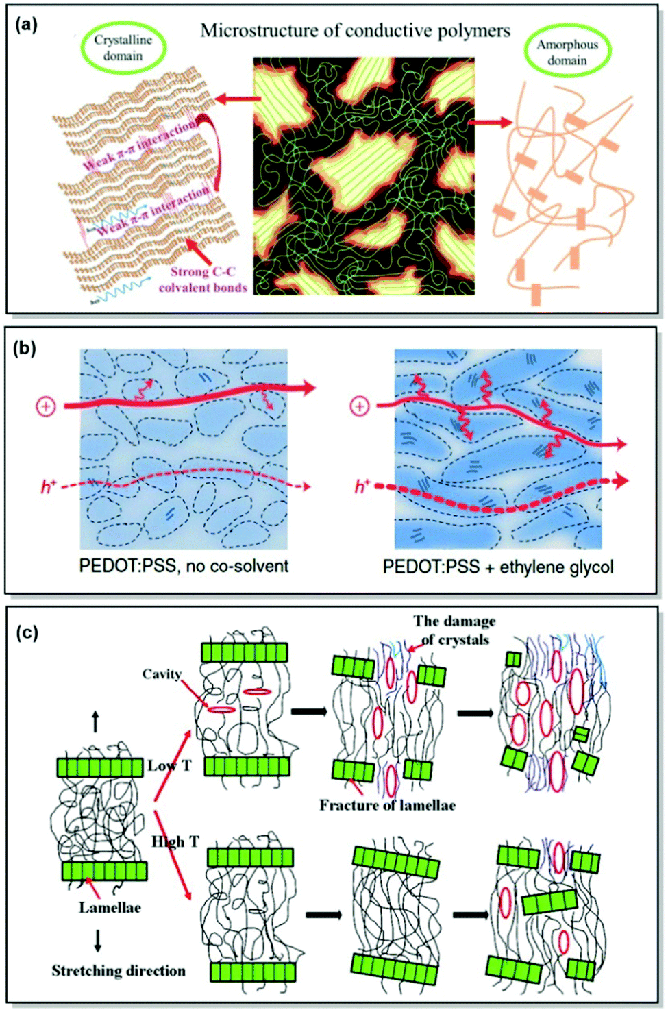 | ||
| Fig. 1 (a) Microstructural features in CPs. Reproduced with permission from Wiley.25 (b) Morphological changes along with associated hole and ion transport in PEDOT:PSS (Scheme 1). The arrows correspond to the intracrystalline hole transport. Reproduced with permission from Springer Nature.26 (c) Strain-induced microstructural changes in a semicrystalline polymer. Reproduced with permission from Elsevier.27 | ||
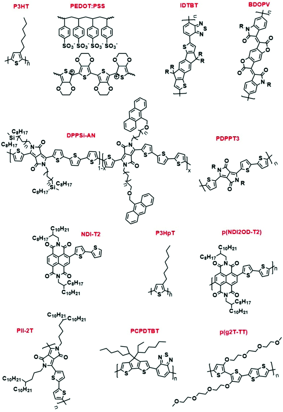 | ||
| Scheme 1 Chemical structures of the polymers discussed in Section 1. | ||
A variety of CPs’ microstructures within a device's active layer is responsible for governing the macroscopic device performances.24 Therefore, it is essential to study the microstructure–property relationship and develop strategies to control molecular packing and film morphology.17 In-depth investigation of CP aggregation, crystallization behaviors, and phase transitions alongside developing new experimental and computational microstructure characterization will help address these limitations.
1.2. State-of-the-art of the CP microstructure research
Multiple research groups have directed their efforts towards the microstructure-property relationship over recent years. Generally, developments in the field of CP microstructure have focused on two main facets: (i) a thorough understanding of CP microstructure; (ii) improving microstructure control. The tools used for both include modification of the chemical structure, establishment of new molecular design rules, physical methods to control the microstructure, and sophisticated computational techniques to predict the morphology and elucidate structure–property interplays.34,45,46 Some selected findings made over the recent 3 years in the field are discussed below.Balanced mechanical properties and charge mobility constitute essential properties of field-effect transistor (FET) memory devices. However, there is just a handful of CP molecular designs, utilizing a side-chain engineering approach to achieve charge-storage capability and stretchability simultaneously. Yen and co-workers investigated intrinsically stretchable diketopyrrolopyrrole (DPP)-based semiconducting polymer DPPSi-AN (Scheme 1), featuring aryl-decorated side chains. Here, incorporating anthracene moieties into the side chains typically reduced polymer crystallinity and enabled electron trapping. Alternatively, carbosilane side chains introduced more free volume into the space. These molecular modifications stabilized hole mobility (0.029 cm2 V−1 s−1 with 53% preservation at 60% tensile strain) and introduced memory-stretchability, desirable for nonvolatile transistor-type memory devices. Superior memory performance was attributed to the incorporation of the anthracene moiety, whose energy levels are conducive to electron trapping and improving hole back-trapping. Additionally, mechanical durability was achieved via microstructure control through side-chain decoration. This work points out that achieving superior intrinsic stretchability and controlling memory-stretchability properties can be enabled by fine-tuning CP crystallinity and judicious choice of side-chain pendants.48
The connection between the nature of the side-chain and CP microstructure was further examined by Feng et al. In the case of OPVs, high charge mobility is often associated with moderately high crystallinity of the active layer. To address this issue, the authors prepared a series of double-cable CPs featuring perylene bisimide units (PBIs) as electron acceptors, connected to the thiophene-based electron donor backbone via flexible linkers. Further, nanostructure evolution and stacking manner between the backbone and the PBI fragments were studied. Feng et al. have demonstrated the impact of linker length on lamellae stacking, which subsequently influences charge mobility and OSC performance. Nanostructural evolution arising from the length of a flexible alkyl linker, connecting the pendant perylene bisimide units with the thiophene-based CP backbone was investigated. Thus, 14+ carbon atoms in a linker were suggested to be necessary to achieve H-aggregation in the reported CP system to form well-ordered nanostructures. These nanostructures decreased geminate recombination loss channels and increased free carrier generation efficiency, leading to high photovoltaic efficiency of 7.3%. This work has confirmed the importance of nanostructures on the OSC performance owing to the balance of charge transport and exciton separation. Double-cable CPs were shown to be promising candidates for highly crystalline CPs with tunable morphology and nanostructure.49
The impact of polymer molecular weight on microstructure, mechanical and electrical properties has also been studied. Through the examination of a series of diketopyrrolopyrrole-based PDPPT3 (Scheme 1) polymers with molecular weight from 8 to 151 kg mol−1, Pei and co-workers showed that relatively high density of tie chains and moderate entanglement lead to optimum crystallinity, considerably high elastic modulus, medium crack-onset strain (CoS) and high mobility. The polymer with a moderate number-average molecular weight of 88 kg mol−1 exhibits the highest elastic modulus and the best hole mobility. These superior characteristics were ascribed to the molecular order, moderate number of entanglements, and continuity of aggregated domains, as revealed by Grazing-Incidence Wide-Angle X-ray Scattering (GIWAXS) and Atomic Force Microscopy (AFM) analysis.50 While CPs with the highest molecular weight are generally more advantageous for stretchable devices, a large number of entanglements at high molecular weight severely decreases charge mobility. The authors have shown that the moderate molecular weight of a CP is crucial to achieving highly stretchable hight-mobility transistors. This work offered valuable guidelines for balancing electrical and mechanical properties in organic semiconductors.
The existence of critical molecular weight on mechanical properties of CPs was further confirmed by Choi et al. By investigating the correlation between the molecular weight, solution entanglement, and film microstructures for a series of D–A thiophene and naphthalene bisimide copolymers P(NDI2OD-T2) (Scheme 1), it was shown that both electron mobility and CoS depend on tie chain density. While charge mobility was found to increase with molecular weight and tie chain number, the opposite relationship was uncovered for CoS, suggesting that the microstructures of high molecular weight polymers with adequate entanglements are promising for mechanically robust semiconducting films.51
Different side chains are also widely used to control the characteristics of OECTs. Volumetric charging of CP electrodes in aqueous electrolytes can be successfully realized through hydrophilic side chains attached to the CP backbone. This approach is known to be conducive to fast electrochemical charging in water solutions. Nevertheless, the relationship between the degree of water uptake by CPs whilst electrochemical charging, on the one hand, and the electrode stability, on the other hand, remained unclear. This was especially valid for the electron-transporting CPs. Szumska et al. have suggested that alternating hydrophilic and hydrophobic side chains on naphthalenetetracarboxylic diimide and bithiophene-based polymers (NDI-T2) (Scheme 1) enables controllable electrolyte uptake and related polymer swelling, as well as reversible red-ox behavior. This was shown to lead to the crucial stability of n-type OMIECs in aqueous media, highlighting the importance of molecular design on electrochemical stability.52
As was discussed previously, understanding crystallization kinetics and examining packing structures is important for controlling CP microstructure. However, both crystallization speed and the effect of the pre-existing microstructural features on CP crystallization have long remained unclear because of strong inter- and intrachain interactions. Therefore, Luo et al. exploited ultrafast scanning calorimetry (FSC) to investigate the crystallization dynamics in DPP-based polymers. According to the authors, the two-step crystallization process allows controlling the degree of crystallinity in CPs and, consequently, manipulating charge mobility is possible. The chain backbone rigidity and the pre-existing crystalline microstructures were proven to affect the crystallization rate of the polymer chains. The crystallization rate increased by over an order of magnitude during the first-step crystallization at the same level of undercooling. Thermal characterization showed that higher crystallinity can be achieved during thermal annealing. That, in turn, leads to higher charge mobility. Overall, the authors have demonstrated that FSC is a plausible method for probing ultrafast crystallization kinetics and examining CP microstructure.54
Comprehension of CP conformation and aggregation in a solution state is useful for controlling the CP properties during solution processing. However, a precise description of solution-state aggregates has not been reported yet. Therefore, Diao and co-workers employed small-angle X-ray scattering (SAXS) in conjunction with SEM and AFM imaging for a thorough analysis of CP freeze-dried solutions. Isoindigo-bithiophene based CP (PII-2T) (Scheme 1) was chosen as a model system for detailed investigation. To elucidate the picture of solution-state aggregation, the authors developed two models to explain D–A polymer scattering. The first model is based on the contribution of two semiflexible cylinders capable of capturing a lamellar peak. The second model takes the hierarchical aggregation of CP chains into fibrils into account. Both models agreed well with freeze-dried imaging results. The second model, in particular, helped to relate the occurrence of a structure factor peak in SAXS data to the stacking of CP side chains within the fibrils. The researchers further checked their assumptions on other D–A CPs with different scattering features to prove the generality of their models. Overall, this study presented SAXS along with direct freeze-dried imaging and described scattering models as a viable method to analyse complicated scattering of D–A CPs. Furthermore, these results are expected to ease the comprehension of CP solution-state conformation and aggregation, which would potentially allow controlling CP structure while solution processing.55
The magnetic field also presents feasible opportunities to control morphology. The method to achieve highly ordered CP films by horizontal rotation in a high magnetic field (HR-HMF) has been recently described by Pan and co-workers. The n-type polymer P(NDI2OD-T2) (Scheme 1) was aligned out-of-plane utilizing horizontal rotation. As a result, an increase from 72% to 98.2% face-on lamellar texture along with a 1.6-fold increase of the π–π stacking crystalline correlation length and an 18-fold enhancement of electron mobility were observed. Of note, magnetic alignment has hardly been used for CPs previously due to insufficient understanding of magnetic response characteristics and sophistication of chemical structures. Therefore, with this work, Pan and co-workers have proven the viability of the HR-HMF method for the achievement of high out-of-plane CP orientation and consequently, high CP charge mobility.56
Aiming to improve the understanding of CP chain rearrangement into ordered structures, Chen's group suggested combining solvent vapor annealing (SVA), real-time AFM, and fluorescence spectroscopy to investigate the morphology of P3HT and para-phenylene ethynylene (PPE) films. Fluorescence spectroscopy is sensitive to changes in intrachain coupling during swelling and restacking. In turn, AFM aids to reveal post-stacking structural information. Hence, the combination of these real-time methods during the polymer SVA allowed for studying CP morphologies on the mesoscopic scale. These findings suggest that spectroscopically monitoring polymer structures in real-time, followed by morphological characterization utilizing AFM during SVA could improve the current understanding of CP chain rearrangement into ordered structures.57
Striving for the crystalline morphology to enhance charge mobility, Wand and co-workers employed epitaxial crystallization of poly[2,6-(4,4-bis-(2-ethylhexyl)-4H-cyclopenta[2,1-b;3,4-b]dithiophene)-alt-4,7(2,1,3 benzothiadiazole)] (PCPDTBT, Scheme 1) on oriented polyethylene (PE) substrates combined with 1,8-diiodooctane (DIO) addition. As a result of these manipulations highly oriented films with a π-stacked form revealed superior carrier mobility (2.1 × 10⁻² cm2 V−1 s−1) measured along the direction of PCPDTBT chains. This mobility proved to be 76 times higher than that measured in the perpendicular direction of molecular chains. This work presented an undemanding method, namely epitaxial crystallization, for managing the crystalline forms of CPs, which would allow for the fabrication of large-area OFETs and OPVs with controlled microstructure.58
Understanding CP morphology is critical for apprehending the ion motion in MIECs. While typically the ion movement during gating is considered, the shifting of neutral ion pairs is rarely taken into consideration. Notably, device speed could be potentially improved if mobile ion pairs are taken up by the semiconductor before gating (passive uptake). In their work, Salleo, Chabinyc, Segalman, McCulloch, and co-workers examined the effects of passive ion uptake on the dynamic and structure of poly(2-(3,3-bis(2-(2-(2-methoxyethoxy)ethoxy)ethoxy)-[2,2′bithiophen]-5-yl)thieno[3,2-b]thiophene), p(g2T-TT) (Scheme 1). Devices with mobile ion pairs, based on gels permeated with ionic liquids, were compared to the ones with immobile ion pairs, utilizing polymerized ionic liquid. According to the XPS data, passive ion pair uptake from the gel to p(g2T-TT) was detected in the first case. In turn, the polymerized ionic liquid was found to prevent the uptake in the second case. X-Ray scattering further confirmed irreversible morphological changes in the lamellar ordering of p(g2T-TT) upon absorbing ion pairs. In situ Raman spectroscopy revealed that both cations and anions get reorganized in a swollen film during gating. Finally, the researchers showed that the speed of MIEC-based neuromorphic devices could be fine-tuned through the control of electrolyte ion movement. This work highlights the importance of investigating ion movement in MIECs and contributes to the comprehension of MIEC doping mechanism.59
As polymer chain length has a direct impact on the resultant morphology, Zozoulenko's group has utilized the MD method to explore simultaneous crystallization of PEDOT at various polymerization temperatures. It was found that while the formation of crystallites starts during the polymerization phase, the crystallization occurs whilst evaporation. Hence, a certain control over the polymer chain length and the dry film morphology was suggested to be possible through the variation of the polymerization and evaporation temperatures. These findings spotlight the importance of applying computational methods, such as MD “computational microscopy”, on investigating CP chain lengths and polymer morphology. In particular, in the case of PEDOT these data cannot be obtained by other means.60
1.3. Motivation for the current study
From the discussion above, it can be seen that a multitude of meaningful contributions towards a deeper understanding of the microstructure-property relationships has been reported in the CP community. Furthermore, various pieces of the puzzle in terms of understanding the interplay between CP microstructure and resulting properties can be collected while investigating copious applications of CPs simultaneously and focusing both on uncovering and controlling polymer microstructure. With these considerations in mind, this feature article aims to provide an overview of the developments in our group, directed at comprehension and command of CP microstructure in many electronic applications. Based on the analysis of published literature and our contribution, the outlook on the future progression of the field will be introduced.2. Key aspects of the recent research in the Luscombe group
2.1. Understanding and control of the microstructure-property relationship in OFETs
As mentioned previously, active layer morphology impacts the device performance of thin-film electronics.61 Therefore, a thorough understanding and control over the morphological parameters are necessary to ensure the adequate performance of CP-based devices. While the majority of research has been dedicated to testing the microstructure-property relationships in thin-film devices post-device fabrication, less has been done to predict and finely control the morphology a priori.62,63 With this motivation in mind, our group has focused on the detailed investigation of CP solid-state morphology. We also took conformational freedom of polymer chains and intermolecular forces governed mesoscale structuring into consideration.P3HT is a workhorse in the field of solution-processable thin-film electronic devices due to its semicrystalline lamellar microstructure, resulting from favourable π–π interactions, and adequate optoelectronic properties, and the ease of precise synthesis.64,65 In the case of the CPs in general and P3HT in particular, control over the microstructure can be achieved through the synthetic control of regioregularity and defects. Attracted by the low cost and multiple applications of P3HT, and armed with extensive expertise in the synthesis of regioregular P3HT, our group has directed significant attention to examining and controlling the microstructure of P3HT. Following up on the original report of controlled externally initiated polymerization toward regioregular (RR) P3HT by Bronstein and Luscombe,66 allowing for a high level of synthetic control, the effect of regioregularity on charge carrier transport in P3HT nanowires was investigated by Mazzio et al.67 Through the comparison of a series of P3HT with 93–99% regioregularity in both thin-film and nanowire transistors, it was established that minor differences in RR, and specifically, higher RR led to a polymer backbone planarity increase, thus correlating with enhanced charge carrier mobility (4-fold increase for the examined RR percentage). In particular, X-ray diffraction and AFM indicated the elongation of the structural coherence in the longitudinal direction, 010, with increasing RR. Due to the relationship between the structural coherence and the average size of crystallites, longer coherence is expected to decrease the number of grain boundary scattering sites. Consequently, charge mobility can be enhanced. Additionally, intrachain order enhancement with regioregularity was confirmed by the observation of J-aggregates, which was shown by the red-shift and intensity increase of the 0-0 UV-Vis absorption peak (Fig. 2).67,68
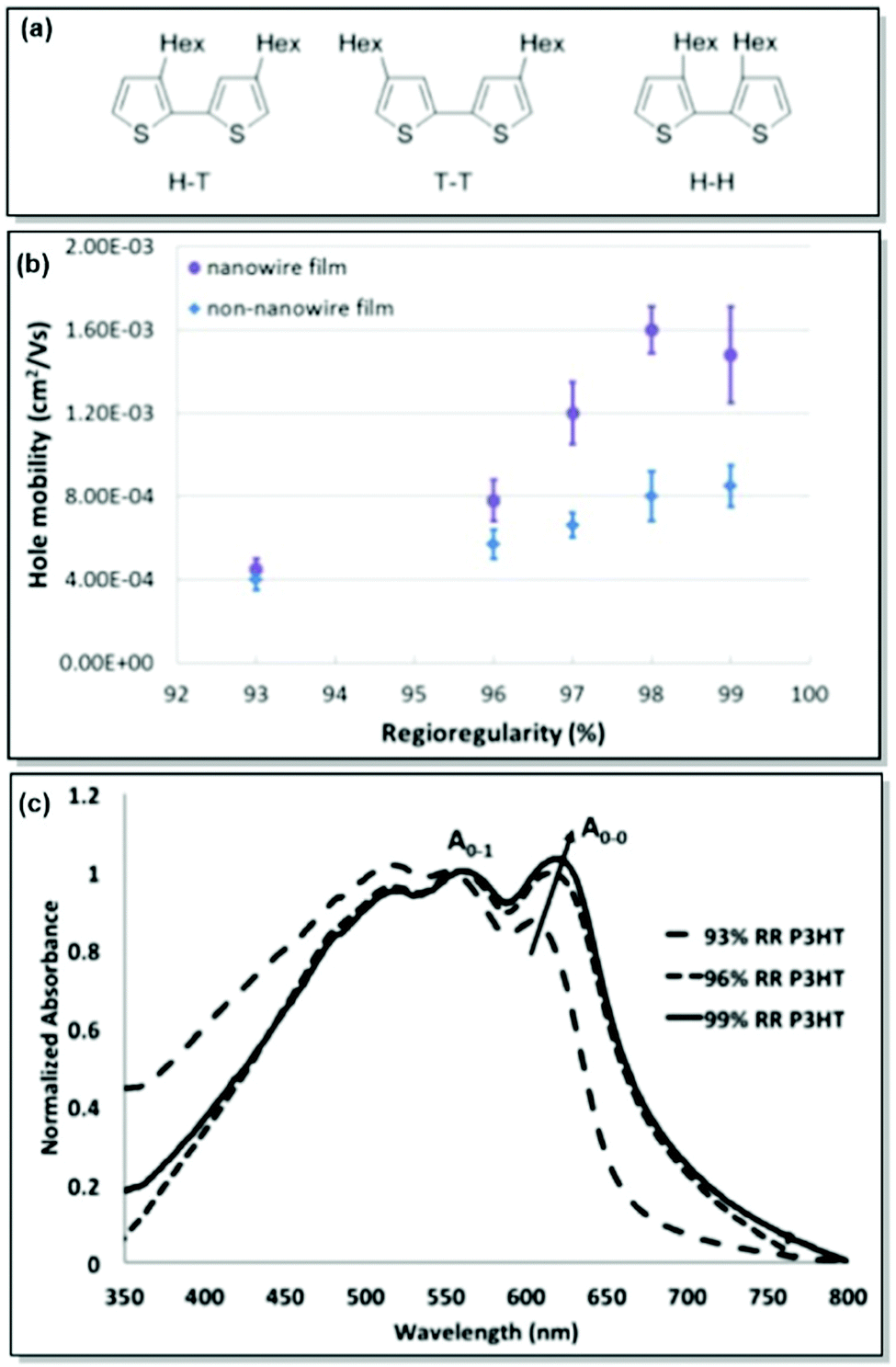 | ||
| Fig. 2 (a) Possible coupling products of P3HT (H–T: head-to-tail, T–T: tail-to-tail, H–H: head-to-head). (b) Correlation between RR and hole mobility for P3HT nanowire and non-nanowire films. (c) UV-Vis absorption spectra for P3HT with various RR%. Reproduced with permission from American Chemical Society.67 | ||
Despite the notable improvement of synthetic precision over the recent years, defects in the chemical structures, hence, the defects in crystal lattices of CPs, remain unavoidable.66,69 As a result, predictive comprehension of the CP morphology and optoelectronic device performance has been difficult to reach. To address this limitation, Tatum et al. suggested a path to quantify the regio-defect tolerance in the crystal lattice of P3HT.70 The authors investigated the effect of strategically incorporated defects, such as bulky bromine atoms and bulky aromatic toluene units, on structural coherence and short-range order of the P3HT crystal lattice. While the possibility of incorporating defects into CP crystal lattice was uncovered, exclusion of the defects by the lattice was found to be preferred. Furthermore, the introduction of the bulky regio-defects was revealed to lessen short-range order and exacerbate the electronic properties of the polymer. However, the authors noted that incorporation of the π–π stacking end groups (e.g., toluene) could be beneficial for crystal growth and long-range order promotion, alleviating crystal lattice disruption (Fig. 3). It was further established, that the enthalpy of fusion for the crystal can be increased by up to 20% via tuning the CP molecular weight to an integer multiple to the observed width of the crystal lamellae. That, consequently, promotes the expulsion of the end groups from the crystal structure. The major takeaway message of this work is the control of the long-range order of the CP lattice via precise synthetic defect incorporation. The long-range order is crucial for such applications as OFET and OPV, where morphology and crystallinity can directly affect the device performance. Additionally, polymer chain folding can ensure accurate defect location and enhance the crystallinity of a nanowire. That is, in turn, translatable to a number of thin layer devices fabricated by deposition methods, such as blade coating.70
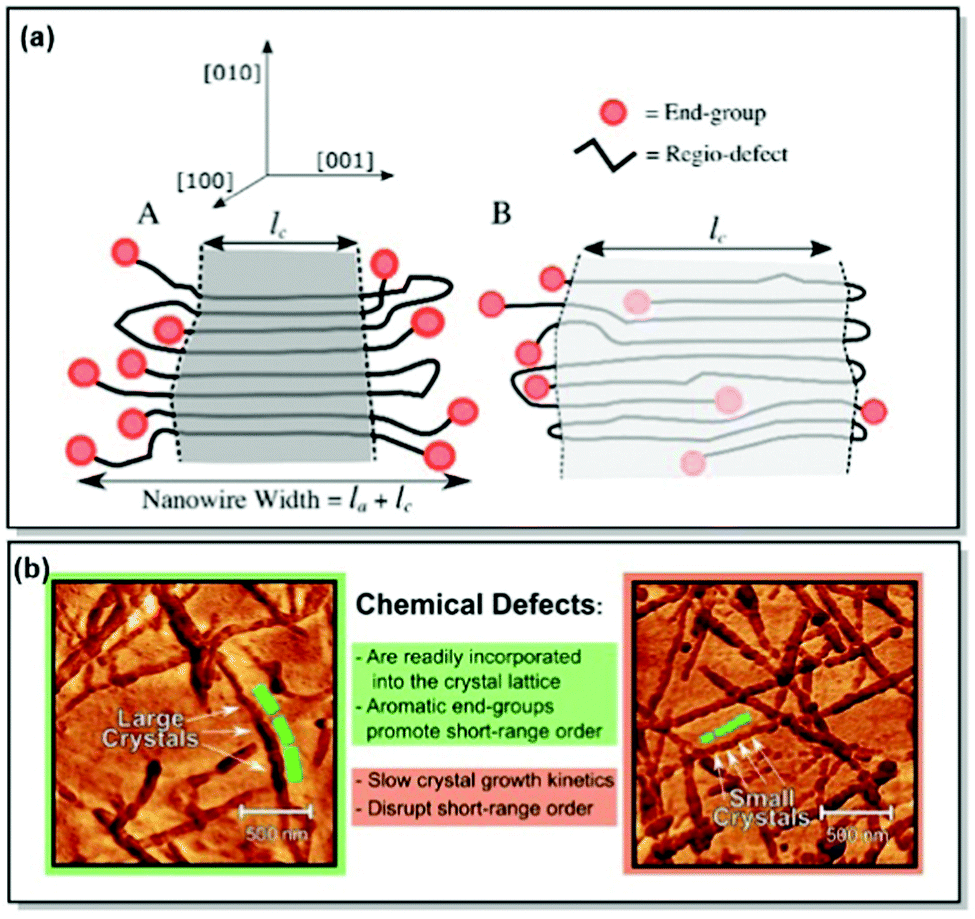 | ||
| Fig. 3 (a) Proposed P3HT nanowire structures with (A) complete or (B) partial defect expulsion, where the darker grey area corresponds to the higher crystallinity region. (b) Young's modulus AFM scans of P3HT nanowires with lower (left panel) and higher (right panel) defect concentration. Reproduced with permission from American Chemical Society.70 | ||
Electrical properties of CPs can be fine-tuned not only through judicious synthesis planning, as in the case of regioregularity control66,67 and strategic defect incorporation.70 Also, the choice of processing conditions, such as solvent engineering,71 casting techniques,72 postdeposition thermal, and solvent–vapor annealing,73 affects the microstructure. All of these methods are capable of changing polymer microstructure and, consequently, charge mobility. Driven by the aim to investigate the interplay of charge transport and intercrystallite structuring, Gu et al. methodically investigated the effect of postdeposition thermal annealing on the samples of P3HT with distinct tie chain fractions, focusing on the role of tie chains, long polymer chains, and bridge neighboring crystallites on the macroscopic charge transport.74 In this work, two P3HT samples, namely P3HT_40 (Mn 40 kg mol−1, tie-chain fraction 6 × 10⁻³) and P3HT_5/40 (homopolymer blend of P3HT with Mn of 5 kg mol−1 and 0.25 weight fraction of P3HT_40), were selected due to the difference in their percolation threshold. These particular P3HT samples, having distinct tie-chain fractions, were selected based on the previous studies. Prior work by Gu et al. suggested the importance of the connectivity between the adjacent crystallites on the microscopic charge transport in P3HT. A critical tie-chain fraction of 10−3 was proven to be essential to assist macroscopic charge transport.75 Upon the examination of the mesoscale packing of P3HT films annealed at different temperatures, it was discovered that while crystallinity is generally increased upon thermal annealing, high temperatures tend to hamper charge transport. In particular, upon careful investigation of differential scanning calorimetry (DSC), GIXRD, UV-Vis absorption, and transistor field-effect mobility data, it was established, that tie-chain pullout occurs during the crystal growth upon thermal annealing. That, in turn, impedes charge transport. Furthermore, the initial amount of tie chains in a sample was found to pre-determine the effect of tie-chain pullout on charge mobility. Thus, as the crystallites in P3HT_5/40 were initially less interconnected compared to P3HT_40, the mobility of the corresponding transistors was more affected by post-deposition annealing in the case of the former. Tie-chain pullout, occurring during crystal growth and thermal annealing, is a driving force behind the morphology and charge transport changes. These results point at the general role of the post-annealing tie-chain pullout on the microstructure of semicrystalline CPs and urge to strive for the optimal thermal annealing temperature to strike the microstructure-property balance (Fig. 4).74
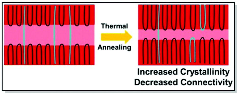 | ||
| Fig. 4 The effect of postdeposition thermal annealing on P3HT_40. Reproduced with permission from American Chemical Society.74 | ||
As mentioned in Section 1.1, amorphous domains feature disordered polymer chains. According to the above example,74 amorphous polymer regions tend to disrupt the inter-chain charge hopping, leading to poor charge mobility. Inter-chain charge hopping, however, can be facilitated by sufficient tie-chain fraction. On the other hand, charge mobility can be improved via ordered phases formation. To increase the CP long-range order and conductivity, and assemble polymer chains into fibers, Xi et al. proposed using acoustic fields at ultrasonic frequencies (420 kHz).76 Polymer molecular structure was found to play a critical role in ultrasound-assisted crystallization. Thus, while generally crystallization of regiorandom RRa-P3HT is prevented by its randomly scattered side chains, sonocrystallization allows the formation of long-range ordered aggregates of this polymer. On the contrary, sonocrystallization was rendered ineffective in the case of regioregular polythiophenes with longer alkyl chains due to their excessive solubility. The authors discovered, that it is possible to assemble P3HT polymer chains into nanofibers by applying ultrasound acoustic waves to the fully dissolved CP. Interestingly, no self-assembling was observed in the polymer solution in the absence of ultrasound. The combination of UV-Vis spectroscopy, ultra-small angle X-ray scattering (USAXS), and small-angle neutron scattering (SANS) allowed suggesting a plausible mechanism of P3HT sonocrystallization. Firstly, it was found that polymer chains do not exist in a thermodynamically stable state even when diffused in good solvents. Secondly, P3HT chains are stabilized by local energy barriers, preventing effective crystallization. Thirdly, ultrasound field application is suggested to generate enough energy to overcome these barriers and promote the formation of small crystalline nuclei, as well as larger crystals. According to Xi, solvent-induced cavitation prompts sonocrystallization to modify CP chain conformation, leading to aggregate formation. As a result, while sonocrystallization provides a facile method of increasing the crystallinity of a polymer, the capacity to sonocrystallize can be correlated with the solubility of a CP.76
As pristine films of CPs are prone to degrade and crack with time, limiting the target device lifespan and applications, CPs are often blended with matrix polymers to mitigate these issues. However, studying blend morphology and microstructure–property relationship is much more complex, compared to that of a pristine CP. Hence, Wolf et al. applied contrast-variation small-angle and ultra-small-angle neutron scattering along with wide-angle X-ray scattering (WAXS) to examine the self-assembly and polymer chain conformation of polythiophene-based CPs in bulk blends with deuterated polystyrene (PS-d8).77 Firstly, phase-separated blend morphology was found to be dependent on CP concentration, forming larger globular domains with the concentration increase. Secondly, polymer regioregularity was demonstrated to affect the shape of the aggregates: while RR-P3HT blends were found to form both nanofibers and semi-crystalline globular regions, regiorandom RRa-P3HT blend was observed to form amorphous globular phase separated morphology. In turn, the introduction of longer side chains, as in the case of dodecyl substituted P3DDT, lead to the observation of semi-crystalline blend morphology. As blend morphology is closely related to conductivity, analysis of the π-stacking-to-lamellar peak height ratio from WAXS results allowed to suggest, that nanofiber formation is essential for fair conductivity. That was observed in RR-P3HT blend. This work underlines the importance of examining the CP blend morphology-charge transport relationships, to choose pertinent processing conditions and improve the device performance.77
2.2. Understanding and control of the microstructure-property relationship in OECTs
Unlike OFETs and OPVs, OECTs operate in aqueous media. The key performance parameters of OECTs, such as electrical, biological, or mechanical response, depend on ionic–electronic coupling, which in turn is tightly connected to the polymer morphology. As a result, designing high-performance MIECs calls for a thorough understanding of polymer structure, morphology, ionic and electronic conduction.78 As discussed in previous sections, CPs generally have a semicrystalline structure, consisting of both crystalline and amorphous zones.33 While electronic transport was proven to occur via crystalline regions with occasional tie-chain assisted hopping between the amorphous zones, exploration of ionic transport is currently a hot topic. Over the last years, our group has contributed immensely to the investigation of the interplay between polymer microstructure and ionic–electronic coupling.As OECT performance relies on dual, electronic and ionic, conductance, MIEC molecular design generally involves a CP scaffold and a polar side chain. Following this design pattern, Flagg, Bischak et al. prepared a novel MIEC polymer, poly(3-{[2-(2-methoxyethoxy)eth-oxy]methyl}thiophene-2,5-diyl) (P3MEEMT), and compared its performance to its alkyl-substituted analogue, P3HT, focusing on the impact of polymer crystallinity on OECT performance.79 Not only did P3MEEMT prove to be a promising material for accumulation-mode OECTs with the transconductance values reaching 49.1 F cm−1 V−1 s−1 in 100 mM KCl, but also it exhibited much faster anion kinetics as compared to P3HT, showing much lesser dependence on anion and cation identity than the latter.79,80 More interestingly, the origin of doping kinetics differences was attributed to the swellability of the semicrystalline structure of each material. Thus, GIXRD results confirmed facilitated P3MEEMT crystal lattice expansion and hydration in solution, allowing for free ionic movement throughout the materials. On the contrary, the crystal lattice of P3HT was able to take in only charge-compensating anions upon ion injection. Investigation of the degree of crystallinity – performance relationship in P3MEEMT points to lower OECT mobility and higher OFET mobility in the case of a more crystalline polymer. Hence, it was concluded that differences in OECT mobility can be related to the hydration of the polymer lattice, influencing the connectivity of crystalline regions. Furthermore, electrochemical quartz crystal microbalance gravimetry (E-QCM) data showed that amorphous polymer film is more subjected to swelling upon hydration than the crystalline film (Fig. 5). However, the disruption of percolation pathways between the crystalline zones leads to overall OECT mobility decrease, as confirmed by photoinduced force microscopy (PiFM) of doped P3MEEMT. The authors also highlight the importance of balance between polymer hydration and the MIEC properties, as excessive hydration can disrupt electronic charge transport.79
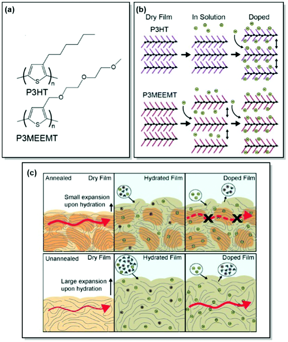 | ||
| Fig. 5 (a) Chemical structures of P3HT and P3MEEMT. (b) Schematic of structural changes in P3HT and P3MEEMT in solution and upon electrochemical doping with P3MEEMT exhibiting a lattice expansion in solution, and the P3HT lattice expanding only upon electrochemical doping (green circles represent anions). (c) Schematic representing charge mobility in annealed and unannealed P3MEEMT (red arrows indicate charge carrier migration through the film). In the dry state, the annealed film is more crystalline and has higher mobility compared to the unannealed sample. When hydrated, the unannealed film swells more and uptakes more electrolyte solution. Lower mobility in the annealed P3MEEMT is assigned to heterogeneity in film swelling. Reproduced with permission from American Chemical Society.79 | ||
Akin to the active polymer materials in OFETs and OPVs, morphology and conductivity in MIECs for OECTs can be controlled through fine-tuning polymer molecular structure, in particular, side chains. Thus, Dong, Nowak, Onorato, et al. conducted a systematic examination of the influence of CP molecular structure on the ion uptake, morphology, and ionic conductivity of two polythiophene-based MIECs.81 Two structurally similar CPs, namely P3MEEMT and P3MEET, lacking an adjacent to the thiophene ring methylene spacer, were thoroughly investigated using electrochemical impedance spectroscopy (EIS), UV-Vis absorption, and GIWAXS. The experimental results were subsequently confirmed by the MD simulations. Structural GIWAXS investigation of thin films of both polymers upon blending with lithium bis-(trifluoromethanesulfonyl)imide (LiTFSI) confirmed preferential infiltration of LiTFSI into amorphous domains, consistently with previous work of Flagg and Bischak.79 Furthermore, crystal structure disruption, leading to lattice strains and considerable drops in the relative degrees of crystallinity, were observed in both polymers upon mixing with LiTFSI, with a more pronounced effect in P3MEET compared to P3MEEMT. Additionally, a starker effect on π–π interaction upon the lithium salt infiltration was discerned in P3MEET compared to P3MEEMT. Amorphous P3MEEMT exhibited higher ionic conductivity than P3MEET at all conditions studied, which was confirmed by theoretical MD simulations (Fig. 6). Such behavior was attributed to the higher segmental mobility of P3MEEMT due to the presence of an additional methylene spacer, as opposed to P3MEET. That resulted in better ionic conductivity in the amorphous zone. Interestingly, a reverse trend was predicted for the crystalline regions of the polymers, which was assigned to the Li+ ion cage formation in P3MEEMT as opposed to P3MEET. This work has not only denoted side-chain engineering as a useful strategy for governing ionic conductivity and morphology but also introduced the duet of experimental and theoretical investigation as a valuable strategy for studying the influence of chemistry on polymer microstructure.81
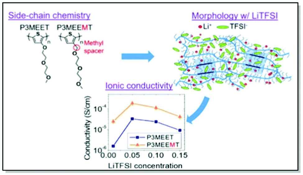 | ||
| Fig. 6 Top-left panel: chemical structures of P3MEET and P3MEEMT. Top-right panel: Schematic representation of LiTFSI distribution within P3MEET/P3MEEMT semicrystalline structure at high concentration of LiTFSI. Bottom panel: P3MEET and P3MEEMT ionic conductivity at 90 °C. Reproduced with permission from American Chemical Society.81 | ||
Searching for a trade-off between the ionic and electronic conductivities in MIECs, Onorato, Wang et al. applied a similar dual theoretical/experimental approach. The authors investigated a series of polythiophenes with varying numbers and positions of oxygen atoms in their side chains.82 In such a manner, the influence of the coordinating group (oxygen) density and position on polymer film morphology and ionic–electronic coupling was examined. MD simulations predicted higher oxygen atom density at a greater distance from the polymer backbone for high ionic conductivity in the case of amorphous systems. On the contrary, decreased number of oxygens and locating the latter at remote positions of the side chain were suggested to maximize the ionic conductivity for the crystalline systems (Fig. 7). The experimental ionic conductivity trends upon doping the polythiophenes with LiTFSI agreed with the MD simulations for the amorphous systems. An additional backbone crystallinity enhancement was observed with increasing oxygen atom distance, leading to improved electronic conductivity. For instance, polythiophene P3APPT, featuring the additional space between the backbone and the side chain oxygens, not only revealed ionic conductivity (5.4 × 10⁻⁴ S cm−1 at 130 °C) comparable to that of P3MEEMT,81 but also displayed enhanced electronic conductivity (3.60 × 10⁻⁵ S cm−1 at 50 °C). Therefore, a valuable strategy to achieve balanced ionic/electronic conductivity via side-chain fine-tuning was presented.82
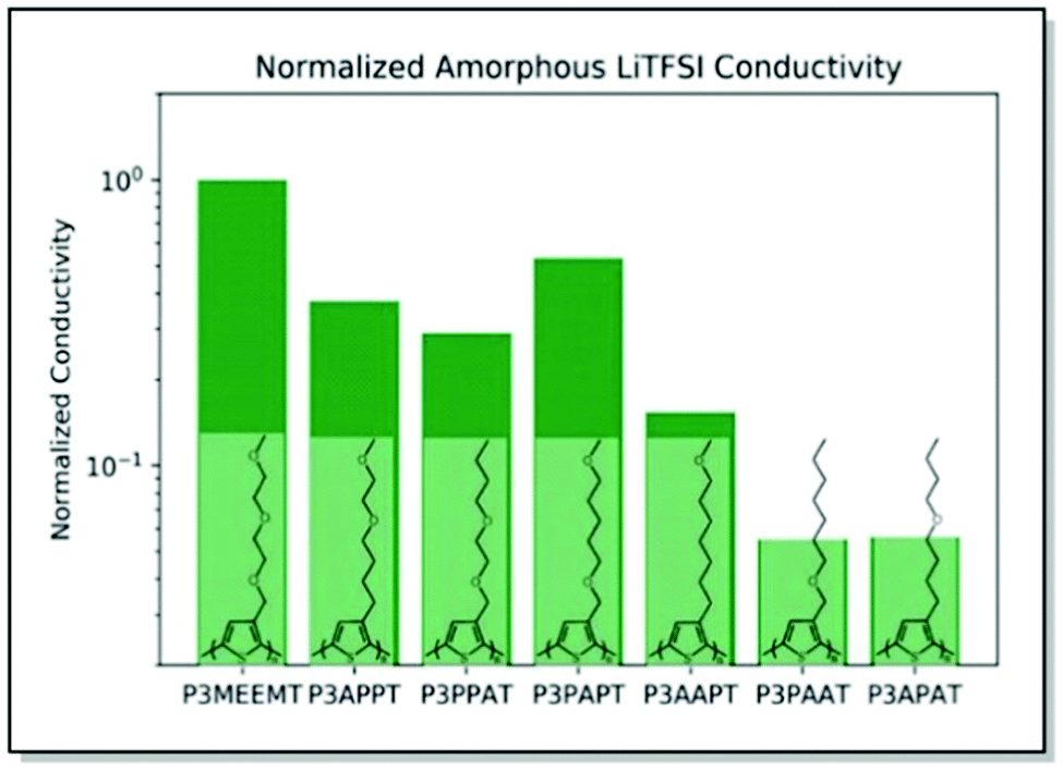 | ||
| Fig. 7 Chemical structures of P3MEEMT, P3APPT, P3PPAT, P3PAPT, P3AAPT, and P3APAT along with the calculated ionic conductivity values for amorphous polymer samples, normalized with the respective polymer dissociation energies, and further normalized against the P3MEEMT performance. Reproduced with permission from Royal Society of Chemistry.82 | ||
Last but not least, Bischak et al. demonstrated, that CPs are capable of undergoing reversible structural phase transitions upon electrochemical ion insertion.83 Through thorough microstructural investigation a unique behavior of poly[2,5-bis(thiophenyl)-1,4-bis(2-(2-(2-methoxyethoxy)ethoxy)-ethoxy)benzene] (PB2T-TEG) upon oxidation/reduction in an aqueous electrolyte was uncovered. Thus, GIWAXS data suggested reversible switches between two structurally distinct crystalline phases of PB2T-TEG upon electrochemical bias. The changes were associated with side-chain melting and the formation of π–π stacking interactions of the polymer backbone in the oxidized state (Fig. 8). Furthermore, significant physical consequences for ion-polaron pair transport were uncovered due to this unique zipping-unzipping microstructural behavior of PB2T-TEG. For instance, optical microscopy and super-resolution PiFM visualization of the moving front experiments revealed non-Fickian transport of ion-polaron pair front in PB2T-TEG, in contrast to the Fickian diffusion in P3MEEMT and its analogues. According to the authors, this distinctive microstructural behavior could be of use for electrochemical properties engineering and neuromorphic memory applications.83
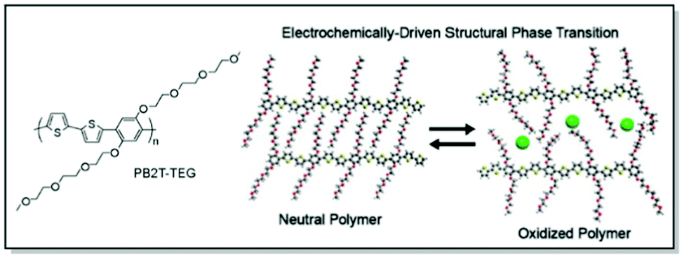 | ||
| Fig. 8 Chemical structure of PB2T-TEG along with the uncovered unzipping/zipping mechanism for ion insertion. Reproduced with permission from American Chemical Society.83 | ||
2.3. Understanding and control of the microstructure-property relationship in the materials for stretchable electronics
As mentioned in Section 1.1, CP deformability, governed both by a rigid conjugated backbone and flexible side chains, is at the heart of flexible and stretchable electronics performance. However, the relationship between the microstructure, mechanical, and electrical properties of CPs is complex. While achieving flexibility is fairly simple, rendering stretchability to a CP is quite challenging, as oftentimes tensile deformation leads to permanent microstructure alterations and affects charge transport.84 According to classical comprehension, crystalline zones are essential for high electronic mobility. At the same time, strong intermolecular interactions, associated with crystallinity, are deleterious for polymer ductility.85,86 Fortunately, recent research proved that the presence of local aggregates and small crystals is sufficient to achieve high mobility.22 As a result, further research efforts were directed to the development of nearly amorphous CPs with high charge mobility and low stiffness.87 In light of these previous findings, the research in our group has focused on the design of intrinsically stretchable high-mobility, high-ductility CPs. Specific attention was dedicated to polymer microstructure and the effects of intermolecular interactions. Some prominent examples of our recent findings will be discussed below.Inspired by the high charge carrier mobility of IDT derivatives, Li et al. designed and prepared an IDT-based donor-acceptor CP PIDTBPD.88 DFT calculations, conducted before the synthesis, suggested that PIDTBPD has a non-planar backbone while showing strong intramolecular charge transfer. This combination of properties could endow the CP with enhanced elasticity and charge mobility, as opposed to more planar structures. The combination of UV-Vis, photoluminescence (PL), DSC, and XRD helped to uncover weak intermolecular interactions between the polymer chains, insuring a nearly amorphous rubbery state of PIDTBPD at room temperature. The experiments also suggested that PIDTBPD undergoes insignificant conformational changes going from solution to the solid state. The results proved that polymer has a rigid backbone despite being non-planar. Indeed, adequate stress-relaxation properties with the elastic modulus of 200 MPa and crack-onset strain of 40% while reaching a high value of charge carrier mobility (2 × 10⁻³ cm2 V−1 s−1) were unveiled for PIDTBPD. These results confirmed the DFT data and paved the way for future research of D–A polymers with a non-planar backbone for stretchable electronics.88
Following up on their original work,88 Li and co-workers continued the exploration of the IDT derivatives, in search of the high-mobility, high ductility, and low elastic modulus CPs. Thus, a series of alkyl-substituted IDT-based D–A polymers with increasing backbone twists was designed employing DFT, synthesized, and investigated. In line with their previous study, the weakest intermolecular interactions were uncovered for PIDTBPD by careful examination of the UV-Vis and PL spectra. That was attributed to the highly twisted skeleton of this polymer (Fig. 9).87 While all three polymers, namely PIDTTPD, PIDTBTD, and PIDTBPD, revealed similar charge transport properties (ca. 0.06–0.2 cm2 V−1 s−1) and comparable glass transition temperatures (−8.1 to 17.6 °C), their mechanical characteristics were found to be quite different. For instance, brittle behavior with CoS values of 3% was elucidated for PIDTTPD and PIDTBTD, featuring planar backbones. At the same time, a twisted skeleton of PIDTBPD led to high ductility and a significantly higher CoS value exceeding 100%. It was suggested that stronger intermolecular interactions are responsible for the suppression of polymer ductility, explaining better mechanical characteristics of the non-planar PIDTBPD. Notably, all three polymers displayed low elastic moduli values (<450 MPa) due to the presence of long, linear alkyl side chains. This work underlines the importance of structure–property investigation of the CPs, suggesting the twisted backbone to be a promising strategy to strike the balance between charge carrier mobility and stretchability.
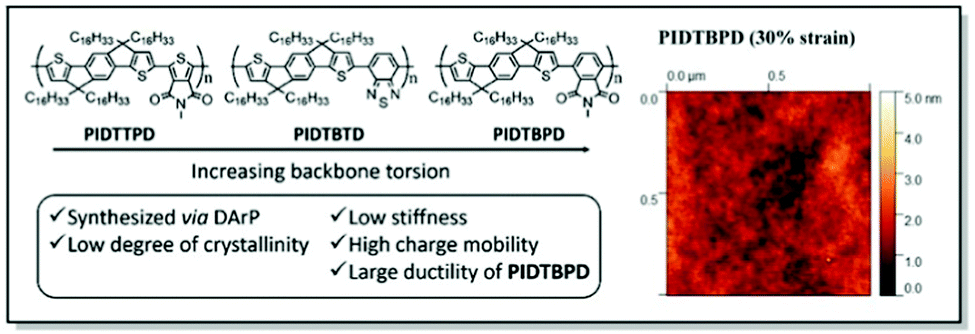 | ||
| Fig. 9 Left panel: Chemical structures of PIDTTPD, PIDTBTD, and PIDTBPD along with the design features; right panel: surface morphology of PIDTBPD under 30% strain obtained using contact mode AFM. Reproduced with permission from American Chemical Society.87 | ||
Sommerville et al. has investigated the connection between the conformational and morphological changes further.38 The authors prepared a series of IDT copolymers with varying ratios of benzothiadiazole (BT) and benzopyrollodione (BPD) units. In this manner, different degrees of twist of the polymer skeleton of the respective copolymers (Fig. 10) were introduced. Interestingly, DFT calculations confirm the absence of substantial differences in the copolymer backbone linearity upon the introduction of the BPD moiety. That is consistent with the GIWAXS results of a similar degree of crystallinity, while polymer planarity is altered. However, the hole mobility of these random copolymer systems was found to be negatively affected by the introduction of the skeleton twist. Variation of the side chain circular distribution around the CP backbone was noted with the increase of BPD share. Fast scanning calorimetry (FSC) data showed that conformational changes, associated with the increase of BPD unit percentage, have a limited impact on the glass transition temperature of the copolymers, confirming similar backbone linearity. It was suggested, that the increase in the BPD content leads to the π-backbone shielding by the circularly distributed side chains. That, in turn, prevents π–π interactions. This side-chain shielding was proposed to facilitate polymer chain sliding during the elongation of the film, resulting in higher CoS. This work, combining an examination of the polymer backbone rigidity and side-chain distribution effects on polymer ductility, allowed to shed more light on the interplay of CP microstructure and mechanical properties.38
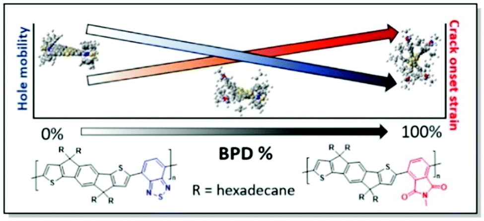 | ||
| Fig. 10 Chemical structures of PIDTBTD and PIDTBPB in the copolymers with various percentages of BPD unit (along with the respective DFT geometries), and the trends of hole mobility and CoS dependence on the BPD share. Reproduced with permission from American Chemical Society.38 | ||
Finally, the role of polymer ties chains on charge-transporting properties of semicrystalline CPs was brought forward in Section 2.1.74 However, even though prior research implied a certain relationship between the tie-chain assisted alignment of the neighboring crystallites and charge mobility increase in the strain direction,89,90 no proof of the tie-chain effect on the mechano-electrical CP characteristics has been reported. With this motivation in mind, Gu et al. chose two samples of regioregular P3HT with known tie-chain fractions, namely P3HT_40 and P3HT_5, to investigate the microstructural changes of the films upon strain and underpin the role of tie chains on the relationship between their electrical and mechanical characteristics.91 By a combination of polarized optical absorbance spectroscopy and GIWAXS, the authors confirmed that tie chains are essential for achieving strain-induced structural alignment. They are also vital for enhancing charge transport in the direction of strain. It was proven, that the lack of tie chains fails to induce significant crystallite reorientation and alignment in the CP (Fig. 11). Instead, polymer sample fracture is observed, with the cracks having a severe impact on charge transport. Therefore, alteration of the tie chain ratios in CPs uncovered a promising strategy to achieve a balance between the electrical and mechanical properties.
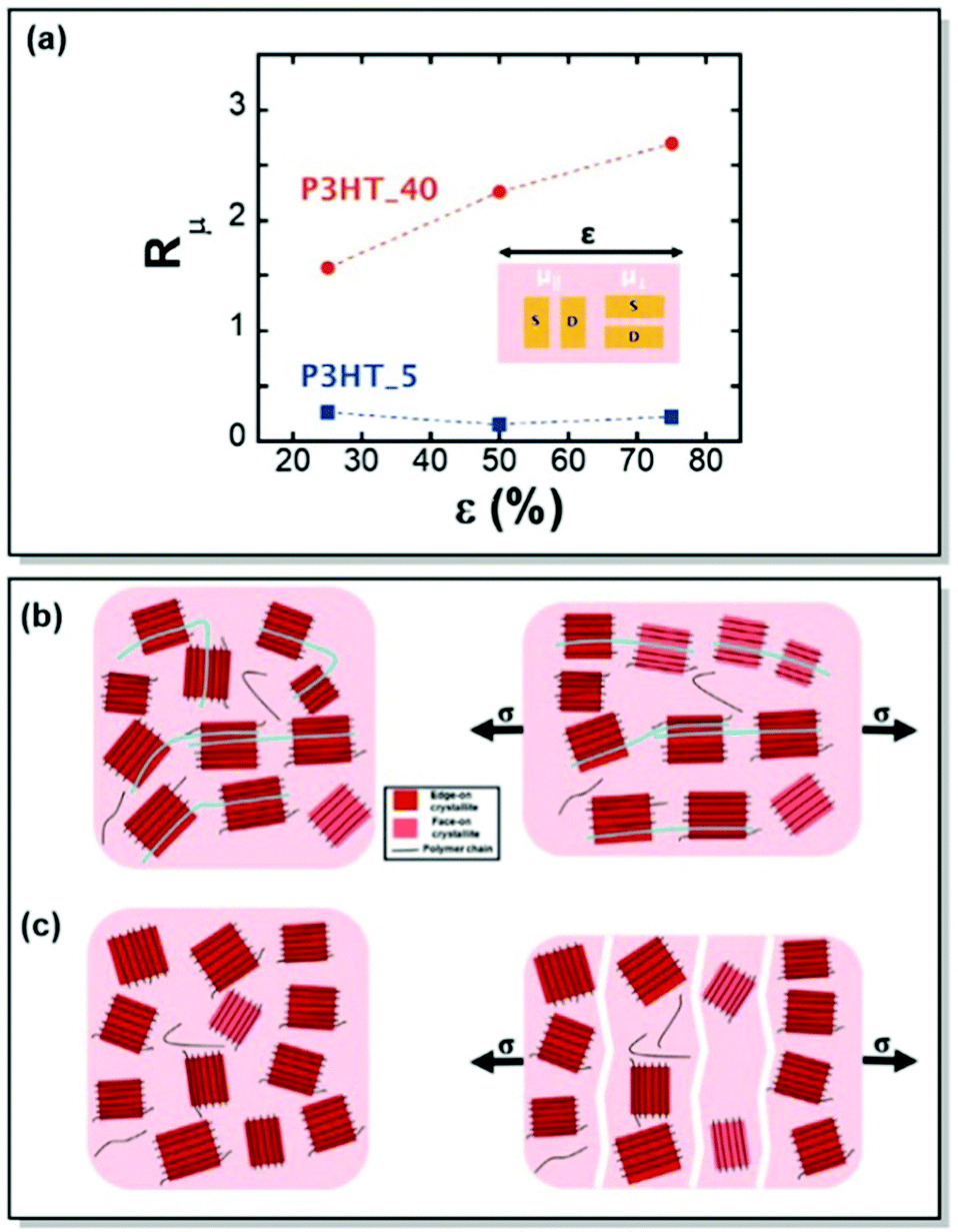 | ||
| Fig. 11 (a) Anisotropy in the field-effect mobility (Rμ) of transistors utilizing P3HT_40 and P3HT_5 thin films, as a function of strain. Schemes of unstrained and strained (b) P3HT_40 and (c) P3HT_5, highlighting the role of tie chains between the crystallites on polymer morphology upon strain. Reproduced with permission from Wiley.91 | ||
2.4. Computational approaches for the morphology/microstructure prediction
The performance and stability bottlenecks72,92–94 for organic electronic devices are strongly dependent on the morphology of the active layer. Without predictable parameters, such as chemical structure, the morphology of the active layer, processing conditions, and target device architecture, the commercialization of functional CPs is hardly possible.95,96 Thus, it can be seen from the discussion in the previous sections of this paper, that a thorough investigation of the microstructure-property relationship of CPs is fairly intensive. Therefore, the need to establish reproducible algorithms for the active layer morphology prediction is useful. Aiming to minimize experimental research efforts, our group has directed its efforts toward the development of generalizable methods for predicting the CP morphology and the related device performance.In an attempt to design an open-access, consumer-friendly morphology interpretation tool, Tatum, Torrejon, O’Neil, and co-workers have developed a widely adaptable Python library, namely m2py. M2py is capable of recognizing various morphological features collected originally by scanning probe microscopy (SPM).97 The toolkit was developed in such a way, that specific functions and modular classes could be assembled into a customizable workflow. The latter aims at the extraction of meaningful details from the SPM data domains, simplifying the application of computer vision techniques. Upon the identification of the data, label maps, displaying quantitative descriptions of the morphological information, are created.
Additionally, m2py toolkit allows for the device performance evaluation, via the analysis of such morphological parameters, as perimeter length, orientation, and aspect ratio (Fig. 12). The versatility of the novel Python toolkit was demonstrated by the application of the workflow to thin films of various homogenous and heterogenous CPs: semicrystalline P3HT in OFETs, self-assembled nanostructures of P3HT spin-coated on indium-tin-oxide (ITO), blended poly[[4,8-bis[(2-ethylhexyl)oxy]benzo[1,2-b:4,5-b′]dithiophene-2,6-diyl][3-fluoro-2-[(2-ethylhexyl)-carbonyl]thieno [3,4-b]thiophenediyl]] (PTB7):PC71BM, and blended P3HT:phenyl-C61-butyric acid methyl ester (PC61BM) in OPV devices. Not only has the compatibility of m2py with any SPM technique been confirmed, but also the capacity of the toolkit to interpret diverse morphological features of a wide range of CPs was successfully demonstrated.
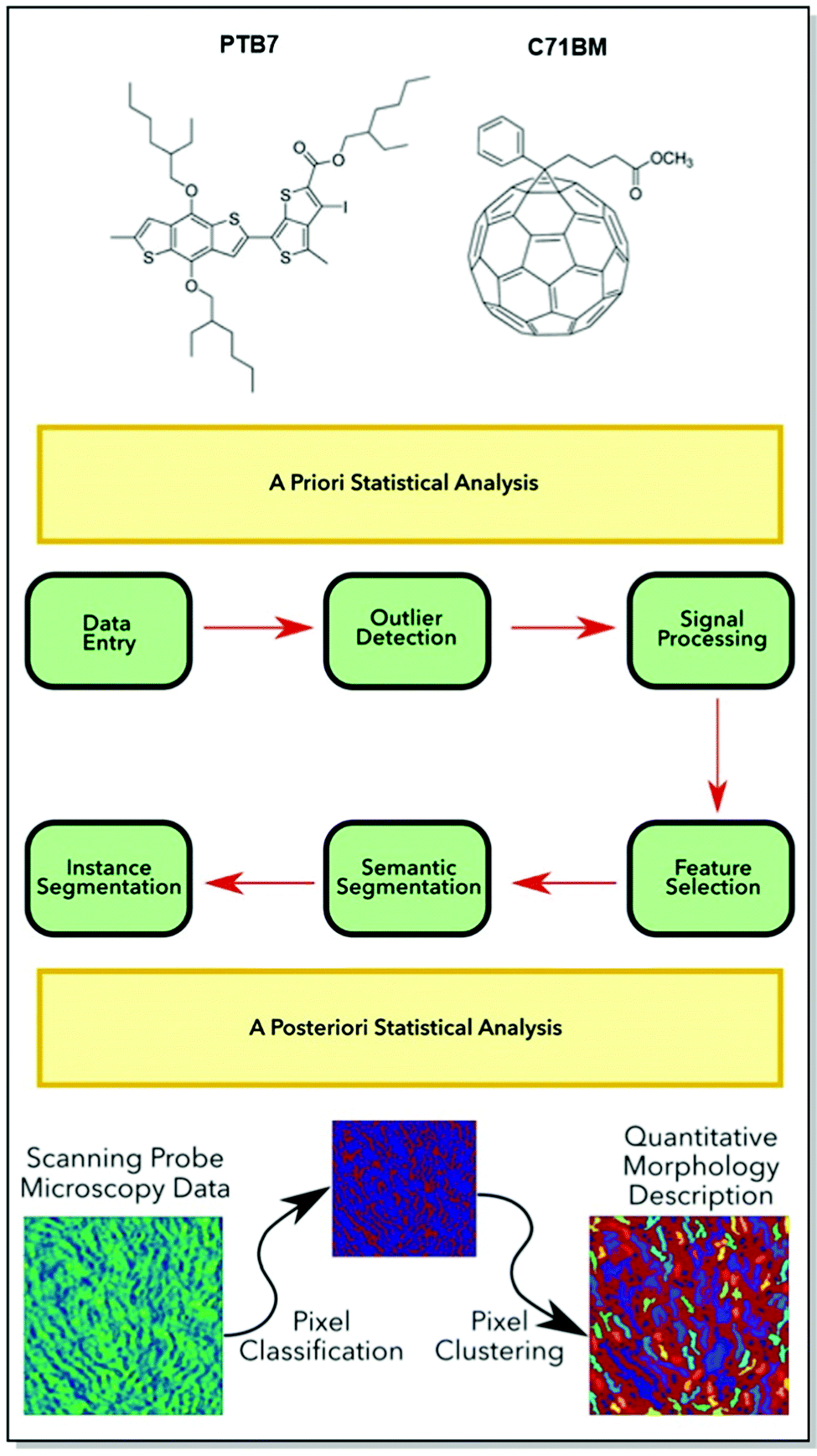 | ||
| Fig. 12 Top panel: Chemical structures of (PTB7):PC71BM. Middle panel: A generalized m2py workflow. Bottom panel: Schematic of the recognition and visualization of the experimental SPM data my the m2py toolkit. Reproduced with permission from American Chemical Society.97 | ||
In their subsequent work, Tatum et al. went a step further. The authors demonstrated, that the Python m2py toolkit97 can be used not only for the identification of the morphological domains obtained by SPM but also for the implication of this quantitative morphology data into predictive models for the device performance.61 To probe their hypothesis, the authors tested a series of bulk heterojunction (BHJ) OPV devices utilizing the blend of well-known P3HT and PC61BM as their active layer.98 The devices were fabricated following the same procedure, however, the post-deposition thermal annealing conditions were purposedly varied to achieve different active layer morphology. The main performance parameters of the OPV devices, namely power conversion efficiency (PCE), fill-factor (FF) open-circuit voltage (Voc), and short-circuit current (Jsc), were measured at various annealing temperatures and times. In turn, active layer surface morphology was imaged using fast force-distance mapping (FDM). M2py was employed to produce morphology-label maps from the original surface morphology data. In the course of this workflow, quantitative morphology overviews were collected, describing the changes in the nanostructures of thin films as a function of thermal annealing. Morphological information, extracted from these images, was further collected and encoded for training predictive models. The accuracy of the predictive model was found to correlate with the amount of the information stored in the library. The prediction error was as low as 1.7% in the case of short-circuit current. Such a small error is indicative of the strong correlation between the OPV device performance and the active layer morphology. As a result, m2py was shown to provide reliable quantitative morphology descriptions, as well as to predict the performance of target OPV devices.61
Last but not least, as DFT and coarse-grained MD calculations are actively employed for the prediction of polymer electronic structure and nonbonded interactions, on the one hand, and chain reptation and diffusion, on the other hand. Wolf et al. has recently revisited the accuracy of MD simulations of CPs, focusing on the discussion of force field development.99 Importantly, the authors highlight the effective usage of neutron scattering in combination with machine learning in enabling high-throughput parametrization of accurate and experimentally validated CP force fields. Consequently, opening additional opportunities for CP microstructure-property relationship investigation and prediction can be uncovered.99
3. Summary and outlook
As a final remark, while polymer microstructure has been an object of research for a long time, the interest in this topic has been reinforced in recent years due to further development and optimization of organic optoelectronic devices, still experiencing performance unpredictability. To control the degree of crystallinity, as well as related charge transporting and mechanical properties, novel CP structures were developed, and new processing methods were proposed. Prediction of CP microstructural features and morphology utilizing computational methods, such as molecular dynamics simulations and artificial intelligence (AI) algorithms, gained more popularity than ever.Our group's research has contributed to several important aspects of the CP microstructure–property investigation: molecular design of the polymers, thorough investigation of processing conditions, employing combinatorial experimental and theoretical approach, and utilizing artificial intelligence to develop microstructure–performance predicting algorithms. In terms of molecular design, target applications of CPs have to be kept in mind. In the case of OFETs and OPVs, a high degree of crystallinity is crucial to ensure high charge carrier mobility. Therefore, control over the long-range order can be gained by managing CP regioregularity, molecular weight, chain folding, and ensuring high tie-chain percentage and precise defect incorporation. OECTs, operating in aqueous electrolyte solutions, in turn, require the balance between the polymer microstructure and ionic–electronic coupling. To strike this balance, the swellability of the polymer lattice and connectivity of the crystalline domains should be carefully supervised. By the combination of experimental and theoretical methods, prudent side-chain engineering was proven to be a successful strategy to enable ionic transport in MIECs without sacrificing electronic conductivity. The lack of strong intermolecular interactions, kinked polymer backbones, and side-chain assisted backbone shielding aimed at chain pullout prevention, in nearly amorphous CPs were identified as crucial conditions to bestow the CP with high ductility and stretchability, without sacrificing charge mobility.
The importance of processing methods, such as post-deposition thermal annealing and sonocrystallization, was also discussed. Controlling the degree of crystallinity of CPs, hence, charge mobility, and reinforcing the role of tie chains in the preservation of the latter, were brought to the forefront. The significance of examining the CP blend morphology-charge transport relationships, aimed at finding pertinent processing conditions and improving the device performance, was underlined.
Finally, reproducible algorithms, based on the application of artificial intelligence and aimed at predicting the relationships between the active layer morphology and the target device performance, were developed as a tool to minimize the experimental research efforts.
While addressing the relationship between the device performance and polymer microstructure, it is important to highlight the significance of device stability.100 A common and often underestimated problem for various applications of organic electronics is the device instability under realistic environmental conditions, including oxygen, moisture, light, high temperatures, and mechanical stress. The reasons for device instability and inadequate operational lifetime are manifold and often system-specific. Apart from the intrinsic organic materials instability, the reasons include charge recombination and charge build-up in multilayer devices, degradation due to oxygen and water penetration, decomposition of the active layer, and contacts at abnormal temperatures.101 Therefore, to ensure reliable device performance, both device architecture, and encapsulation techniques should be developed in conjunction with the design of novel oxygen-, humidity- and temperature-resistant organic semiconductors.
The diversity and scope of these findings, spanning across chemistry, physics, and artificial intelligence, and involving CPs for a plethora of applications, have allowed us to form a fairly clear broad picture of the interplay between the CP molecular design, microstructure, and properties. We envision future research efforts to be directed at: (i) further facile molecular designs and processing development, allowing for the precise control of polymer microstructure; (ii) the expansion of the characterization methods toolbox, focusing on in situ methods in particular; (iii) establishment of new computational and AI methods for accurate microstructure–property relationship prediction. On the whole, a zooming-in trend of looking into the morphology of an individual film rather than focusing on the investigation of multiple devices is expected. Following these broad tendencies, our group's research is likely to be focused on the following facets of CP microstructure research: (i) striving for a unified understanding of microstructure formation by employing precise defect engineering in various CP nanowires and correlating polymer nanowire structure to thin-film properties; (ii) reducing intercrystallite disorder, i.e., paracrystallinity, via controlling polymer side chain ordering; (iii) investigation of CP microstructure upon doping and blending; (iv) development of new computational methods with broadened parameterization, allowing for more careful capture of polymer structure and dynamics; (v) expansion of the AI-based generalizable workflows towards reliable microstructure-property prediction. Overall, we envisage that reinforced attention to the active layer microstructure in relation to the device properties will not only bridge the gap in device performance understanding but would also allow for cost reduction in device fabrication.
Conflicts of interest
There are no conflicts to declare.Notes and references
- T. Nezakati, A. Seifalian, A. Tan and A. M. Seifalian, Chem. Rev., 2018, 118, 6766–6843 CrossRef CAS PubMed.
- A. T. Kleinschmidt and D. J. Lipomi, Acc. Chem. Res., 2018, 51, 3134–3143 CrossRef CAS PubMed.
- S. Inal, J. Rivnay, A. O. Suiu, G. G. Malliaras and I. McCulloch, Acc. Chem. Res., 2018, 51, 1368–1376 CrossRef CAS PubMed.
- X. Jiang, J. Yang, S. Karuthedath, J. Li, W. Lai, C. Li, C. Xiao, L. Ye, Z. Ma, Z. Tang, F. Laquai and W. Li, Angew. Chemie, 2020, 132, 21867–21876 CrossRef.
- Y. Liu, C. Li, Z. Ren, S. Yan and M. R. Bryce, Nat. Rev. Mater., 2018, 3, 1–20 CrossRef.
- G. Gao, M. Chen, J. Roberts, M. Feng, C. Xiao, G. Zhang, S. Parkin, C. Risko and L. Zhang, J. Am. Chem. Soc., 2020, 142, 2460–2470 CrossRef CAS.
- J. Wang, Y. Liu, L. Hua, T. Wang, H. Dong, H. Li, X. Sun, Z. Ren and S. Yan, ACS Appl. Polym. Mater., 2021, 3, 2098–2108 CrossRef CAS.
- X. Li, B. Hu, M. Zhang, X. Wang, L. Chen, A. Wang, Y. Wang, Z. Du, L. Jiang, H. Liu, X. Li, M. Zhang, L. Jiang, H. Liu, B. Hu, X. Wang, L. Chen, A. Wang, Z. Du and Y. Wang, Adv. Mater., 2019, 31, 1904610 CrossRef CAS PubMed.
- J. Rivnay, S. Inal, A. Salleo, R. M. Owens, M. Berggren and G. G. Malliaras, Nat. Rev. Mater., 2018, 3, 17086 CrossRef CAS.
- P. Leleux, J. Rivnay, T. Lonjaret, J.-M. Badier, C. Bénar, T. Hervé, P. Chauvel and G. G. Malliaras, Adv. Healthcare Mater., 2015, 4, 142–147 CrossRef CAS PubMed.
- S. Inal, G. G. Malliaras and J. Rivnay, Nat. Commun., 2017, 8, 1–7 CrossRef CAS.
- J. C. Yang, J. Mun, S. Y. Kwon, S. Park, Z. Bao and S. Park, Adv. Mater., 2019, 31, 1904765 CrossRef CAS.
- D. McCoul, W. Hu, M. Gao, V. Mehta, Q. Pei, D. McCoul, W. Hu, M. Gao, V. Mehta and Q. Pei, Adv. Electron. Mater., 2016, 2, 1500407 CrossRef.
- C. Wang, T. Yokota and T. Someya, Chem. Rev., 2021, 121, 2109–2146 CrossRef CAS PubMed.
- H. Joo, Y. Lee, J. Kim, J. S. Yoo, S. Yoo, S. Kim, A. K. Arya, S. Kim, S. H. Choi, N. Lu, H. S. Lee, S. Kim, S. T. Lee and D. H. Kim, Sci. Adv., 2021, 7, eabd4639 CrossRef CAS PubMed.
- G. H. Lee, H. Moon, H. Kim, G. H. Lee, W. Kwon, S. Yoo, D. Myung, S. H. Yun, Z. Bao and S. K. Hahn, Nat. Rev. Mater., 2020, 5, 149–165 CrossRef.
- Z. Ding, D. Liu, K. Zhao and Y. Han, Macromolecules, 2021, 54, 3907–3926 CrossRef CAS.
- T. Qin and A. Troisi, J. Am. Chem. Soc., 2013, 135, 11247–11256 CrossRef CAS PubMed.
- X. Zhang, H. Bronstein, A. J. Kronemeijer, J. Smith, Y. Kim, R. J. Kline, L. J. Richter, T. D. Anthopoulos, H. Sirringhaus, K. Song, M. Heeney, W. Zhang, I. McCulloch and D. M. Delongchamp, Nat. Commun., 2013, 4, 1–9 Search PubMed.
- C. Cendra, L. Balhorn, W. Zhang, K. O’Hara, K. Bruening, C. J. Tassone, H. G. Steinrück, M. Liang, M. F. Toney, I. McCulloch, M. L. Chabinyc, A. Salleo and C. J. Takacs, ACS Macro Lett., 2021, 10, 1306–1314 CrossRef CAS.
- X. Shen, W. Hu and T. P. Russell, Macromolecules, 2016, 49, 4501–4509 CrossRef CAS.
- R. Noriega, J. Rivnay, K. Vandewal, F. P.-V. Koch, N. Stingelin, P. Smith, M. F. Toney and A. Salleo, Nat. Mater., 2013, 12, 1038–1044 CrossRef CAS.
- I. Osaka and K. Takimiya, Polymer, 2015, 59, A1–A15 CrossRef CAS.
- L. Deng and G. Chen, Nano Energy, 2021, 80, 105448 CrossRef CAS.
- Y. Wang, L. Yang, X. L. Shi, X. Shi, L. Chen, M. S. Dargusch, J. Zou and Z. G. Chen, Adv. Mater., 2019, 31, 1807916 CrossRef PubMed.
- J. Rivnay, S. Inal, B. A. Collins, M. Sessolo, E. Stavrinidou, X. Strakosas, C. Tassone, D. M. Delongchamp and G. G. Malliaras, Nat. Commun., 2016, 7, 1–9 Search PubMed.
- X. Zhang, K. Schneider, G. Liu, J. Chen, K. Brüning, D. Wang and M. Stamm, Polymer, 2012, 53, 648–656 CrossRef CAS.
- H. Sirringhaus, T. Sakanoue and J. F. Chang, Phys. Status Solidi, 2012, 249, 1655–1676 CrossRef CAS.
- F. Laquai, G. Wegner and H. Bässler, Philos. Trans. R. Soc., A, 2007, 365, 1473–1487 CrossRef CAS.
- V. Lemaur, J. Cornil, R. Lazzaroni, H. Sirringhaus, D. Beljonne and Y. Olivier, Chem. Mater., 2019, 31, 6889–6899 CrossRef CAS.
- N. Zhao, Y. Y. Noh, J. F. Chang, M. Heeney, I. McCulloch and H. Sirringhaus, Adv. Mater., 2009, 21, 3759–3763 CrossRef CAS.
- T. Liu and A. Troisi, Adv. Funct. Mater., 2014, 24, 925–933 CrossRef CAS.
- S. A. Mollinger, B. A. Krajina, R. Noriega, A. Salleo and A. J. Spakowitz, ACS Macro Lett., 2015, 4, 708–712 CrossRef CAS.
- I. Botiz and N. Stingelin, Mater., 2014, 7, 2273–2300 CrossRef PubMed.
- K. Gu and Y. L. Loo, J. Polym. Sci., Part B: Polym. Phys., 2019, 57, 1559–1571 CrossRef CAS.
- Z. Bao, A. Dodabalapur and A. J. Lovinger, Appl. Phys. Lett., 1998, 69, 4108 CrossRef.
- Y. Zheng, G. J.-N. Wang, J. Kang, M. Nikolka, H. C. Wu, H. Tran, S. Zhang, H. Yan, H. Chen, P. Y. Yuen, J. Mun, R. H. Dauskardt, I. McCulloch, J. B.-H. Tok, X. Gu and Z. Bao, Adv. Funct. Mater., 2019, 29, 1905340 CrossRef CAS.
- P. J.-W. Sommerville, Y. Li, B. X. Dong, Y. Zhang, J. W. Onorato, W. K. Tatum, A. H. Balzer, N. Stingelin, S. N. Patel, P. F. Nealey and C. K. Luscombe, Macromolecules, 2020, 53, 7511–7518 CrossRef CAS.
- B. D. Paulsen, S. Fabiano and J. Rivnay, Annu. Rev. Mater. Res., 2021, 51, 73–99 CrossRef CAS.
- J. F. Franco-Gonzalez and I. V. Zozoulenko, J. Phys. Chem. B, 2017, 121, 4299–4307 CrossRef CAS.
- M. Matta, R. Wu, B. D. Paulsen, A. J. Petty, R. Sheelamanthula, I. McCulloch, G. C. Schatz and J. Rivnay, Chem. Mater., 2020, 32, 7301–7308 CrossRef CAS.
- R. Demets, M. Grodent, K. Van Kets, S. De Meester and K. Ragaert, Polymers, 2022, 14, 239 CrossRef CAS.
- F. P.-V. Koch, J. Rivnay, S. Foster, C. Müller, J. M. Downing, E. Buchaca-Domingo, P. Westacott, L. Yu, M. Yuan, M. Baklar, Z. Fei, C. Luscombe, M. A. McLachlan, M. Heeney, G. Rumbles, C. Silva, A. Salleo, J. Nelson, P. Smith and N. Stingelin, Prog. Polym. Sci., 2013, 38, 1978–1989 CrossRef CAS.
- R. Xie, A. R. Weisen, Y. Lee, M. A. Aplan, A. M. Fenton, A. E. Masucci, F. Kempe, M. Sommer, C. W. Pester, R. H. Colby and E. D. Gomez, Nat. Commun., 2020, 11, 1–8 CrossRef PubMed.
- M. Li, H. Bin, X. Jiao, M. M. Wienk, H. Yan and R. A.-J. Janssen, Angew. Chemie, 2020, 132, 856–862 CrossRef.
- X. Liu, Y. Yan, Q. Zhang, K. Zhao and Y. Han, Chem. Res. Chin. Univ., 2021, 37, 1019–1030 CrossRef CAS.
- Y. Q. Zheng, Z. F. Yao, J. H. Dou, Y. Wang, W. Ma, L. Zou, S. Nikzad, Q. Y. Li, Z. H. Sun, Z. A. Yu, W. Bin Zhang, J. Y. Wang and J. Pei, Giant, 2021, 7, 100064 CrossRef CAS.
- H. C. Yen, Y. C. Lin and W. C. Chen, ACS Appl. Polym. Mater., 2021, 3, 6416–6426 CrossRef CAS.
- G. Feng, W. Tan, S. Karuthedath, C. Li, X. Jiao, A. C.-Y. Liu, H. Venugopal, Z. Tang, L. Ye, F. Laquai, C. R. McNeill and W. Li, Angew. Chem., Int. Ed., 2021, 60, 25499–25507 CrossRef CAS.
- D. Pei, Z. Wang, Z. Peng, J. Zhang, Y. Deng, Y. Han, L. Ye and Y. Geng, Macromolecules, 2020, 53, 4490–4500 CrossRef CAS.
- J. Choi, W. Kim, D. Kim, S. Kim, J. Chae, S. Q. Choi, F. S. Kim, T. S. Kim and B. J. Kim, Chem. Mater., 2019, 31, 3163–3173 CrossRef CAS.
- A. A. Szumska, I. P. Maria, L. Q. Flagg, A. Savva, J. Surgailis, B. D. Paulsen, D. Moia, X. Chen, S. Griggs, J. T. Mefford, R. B. Rashid, A. Marks, S. Inal, D. S. Ginger, A. Giovannitti and J. Nelson, J. Am. Chem. Soc., 2021, 143, 14795–14805 CrossRef CAS PubMed.
- K. Choudhary, A. X. Chen, G. M. Pitch, R. Runser, A. Urbina, T. J. Dunn, M. Kodur, A. T. Kleinschmidt, B. G. Wang, J. A. Bunch, D. P. Fenning, A. L. Ayzner and D. J. Lipomi, ACS Appl. Mater. Interfaces, 2021, 13, 51436–51446 CrossRef CAS PubMed.
- S. Luo, N. Li, S. Zhang, C. Zhang, T. Qu, M. U. Ocheje, G. Xue, X. Gu, S. Rondeau-Gagné, W. Hu, S. Wang, C. Teng, D. Zhou and J. Xu, Chem. Mater., 2021, 33, 1637–1647 CrossRef CAS.
- J. J. Kwok, K. S. Park, B. B. Patel, R. Dilmurat, D. Beljonne, X. Zuo, B. Lee and Y. Diao, Chemrxiv, 2021 DOI:10.26434/CHEMRXIV-2021-KNXG8.
- G. Pan, L. Hu, F. Zhang and Q. Chen, J. Phys. Chem. Lett., 2021, 12, 3476–3484 CrossRef CAS PubMed.
- H. C. Chou, W. C. Hsu, Y. Yang, K. S. Schanze, S. C. Luo and C. Chen, Macromol. Chem. Phys., 2021, 222, 2100135 CrossRef CAS.
- J. Wang, Y. Liu, L. Hua, T. Wang, H. Dong, H. Li, X. Sun, Z. Ren and S. Yan, ACS Appl. Polym. Mater., 2021, 3, 2098–2108 CrossRef CAS.
- T. J. Quill, G. LeCroy, A. Melianas, D. Rawlings, Q. Thiburce, R. Sheelamanthula, C. Cheng, Y. Tuchman, S. T. Keene, I. McCulloch, R. A. Segalman, M. L. Chabinyc and A. Salleo, Adv. Funct. Mater., 2021, 31, 2104301 CrossRef CAS.
- D. Kim, J. F. Franco-Gonzalez and I. Zozoulenko, J. Phys. Chem. B, 2021, 125, 10324–10334 CrossRef CAS PubMed.
- W. K. Tatum, D. Torrejon, A. B. Resing, J. W. Onorato and C. K. Luscombe, Comput. Mater. Sci., 2021, 197, 110599 CrossRef.
- V. Savikhin, M. Babics, M. Neophytou, S. Liu, S. D. Oosterhout, H. Yan, X. Gu, P. M. Beaujuge and M. F. Toney, Chem. Mater., 2018, 30, 7872–7884 CrossRef CAS.
- C. J. Cho, S. Y. Chen, C. C. Kuo, L. Veeramuthu, A. N. Au-Duong, Y. C. Chiu and S. H. Chang, Polym. J., 2018, 50, 975–987 CrossRef CAS.
- A. Facchetti, Chem. Mater., 2010, 23, 733–758 CrossRef.
- R. Miyakoshi, A. Yokoyama and T. Yokozawa, J. Am. Chem. Soc., 2005, 127, 17542–17547 CrossRef CAS PubMed.
- H. A. Bronstein and C. K. Luscombe, J. Am. Chem. Soc., 2009, 131, 12894–12895 CrossRef CAS PubMed.
- K. A. Mazzio, A. H. Rice, M. M. Durban and C. K. Luscombe, J. Phys. Chem. C, 2015, 119, 14911–14918 CrossRef CAS.
- F. C. Spano, Acc. Chem. Res., 2010, 43, 429–439 CrossRef CAS PubMed.
- Y. Huang and C. K. Luscombe, Chem. Rec., 2019, 19, 1039–1049 CrossRef CAS PubMed.
- W. K. Tatum, A. B. Resing, L. Q. Flagg, D. S. Ginger and C. K. Luscombe, ACS Appl. Polym. Mater., 2019, 1, 1466–1475 CrossRef CAS.
- N. Kleinhenz, N. Persson, Z. Xue, P. H. Chu, G. Wang, Z. Yuan, M. A. McBride, D. Choi, M. A. Grover and E. Reichmanis, Chem. Mater., 2016, 28, 3905–3913 CrossRef CAS.
- H. N. Tsao, D. Cho, J. W. Andreasen, A. Rouhanipour, D. W. Breiby, W. Pisula and K. Müllen, Adv. Mater., 2009, 21, 209–212 CrossRef CAS.
- C. Dingler, K. Dirnberger and S. Ludwigs, Macromol. Rapid Commun., 2019, 40, 1800601 CrossRef PubMed.
- K. Gu, Y. Wang, R. Li, E. Tsai, J. W. Onorato, C. K. Luscombe, R. D. Priestley and Y. L. Loo, ACS Appl. Mater. Interfaces, 2021, 13, 999–1007 CrossRef CAS PubMed.
- K. Gu, C. R. Snyder, J. Onorato, C. K. Luscombe, A. W. Bosse and Y. L. Loo, ACS Macro Lett., 2018, 7, 1333–1338 CrossRef CAS.
- Y. Xi, D. S. Li, G. M. Newbloom, W. K. Tatum, M. O’Donnell, C. K. Luscombe and L. D. Pozzo, Soft Matter, 2018, 14, 4963–4976 RSC.
- C. M. Wolf, L. Guio, S. C. Scheiwiller, R. P. O’Hara, C. K. Luscombe and L. D. Pozzo, Macromolecules, 2021, 54, 2960–2978 CrossRef CAS.
- R. Giridharagopal, L. Q. Flagg, J. S. Harrison, M. E. Ziffer, J. Onorato, C. K. Luscombe and D. S. Ginger, Nat. Mater., 2017, 16, 737–742 CrossRef CAS PubMed.
- L. Q. Flagg, C. G. Bischak, J. W. Onorato, R. B. Rashid, C. K. Luscombe and D. S. Ginger, J. Am. Chem. Soc., 2019, 141, 4345–4354 CrossRef CAS PubMed.
- L. Q. Flagg, C. G. Bischak, R. J. Quezada, J. W. Onorato, C. K. Luscombe and D. S. Ginger, ACS Mater. Lett., 2020, 2, 254–260 CrossRef CAS.
- B. X. Dong, C. Nowak, J. W. Onorato, J. Strzalka, F. A. Escobedo, C. K. Luscombe, P. F. Nealey and S. N. Patel, Chem. Mater., 2019, 31, 1418–1429 CrossRef CAS.
- J. W. Onorato, Z. Wang, Y. Sun, C. Nowak, L. Q. Flagg, R. Li, B. X. Dong, L. J. Richter, F. A. Escobedo, P. F. Nealey, S. N. Patel and C. K. Luscombe, J. Mater. Chem. A, 2021, 9, 21410–21423 RSC.
- C. G. Bischak, L. Q. Flagg, K. Yan, T. Rehman, D. W. Davies, R. J. Quezada, J. W. Onorato, C. K. Luscombe, Y. Diao, C. Z. Li and D. S. Ginger, J. Am. Chem. Soc., 2020, 142, 7434–7442 CrossRef CAS PubMed.
- J. Y. Oh, S. Rondeau-Gagné, Y. C. Chiu, A. Chortos, F. Lissel, G. J.-N. Wang, B. C. Schroeder, T. Kurosawa, J. Lopez, T. Katsumata, J. Xu, C. Zhu, X. Gu, W. G. Bae, Y. Kim, L. Jin, J. W. Chung, J. B.-H. Tok and Z. Bao, Nature, 2016, 539, 411–415 CrossRef CAS PubMed.
- B. Roth, S. Savagatrup, N. V. De Los Santos, O. Hagemann, J. E. Carlé, M. Helgesen, F. Livi, E. Bundgaard, R. R. Søndergaard, F. C. Krebs and D. J. Lipomi, Chem. Mater., 2016, 28, 2363–2373 CrossRef CAS.
- J. Onorato, V. Pakhnyuk and C. K. Luscombe, Polym. J., 2016, 49, 41–60 CrossRef.
- Y. Li, W. K. Tatum, J. W. Onorato, Y. Zhang and C. K. Luscombe, Macromolecules, 2018, 51, 6352–6358 CrossRef CAS.
- Y. Li, W. K. Tatum, J. W. Onorato, S. D. Barajas, Y. Y. Yang and C. K. Luscombe, Polym. Chem., 2017, 8, 5185–5193 RSC.
- B. T. O’Connor, O. G. Reid, X. Zhang, R. J. Kline, L. J. Richter, D. J. Gundlach, D. M. Delongchamp, M. F. Toney, N. Kopidakis and G. Rumbles, Adv. Funct. Mater., 2014, 24, 3422–3431 CrossRef.
- D. Wu, M. Kaplan, H. W. Ro, S. Engmann, D. A. Fischer, D. M. DeLongchamp, L. J. Richter, E. Gann, L. Thomsen, C. R. McNeill and X. Zhang, Chem. Mater., 2018, 30, 1924–1936 CrossRef CAS.
- K. Gu, J. W. Onorato, C. K. Luscombe and Y. L. Loo, Adv. Electron. Mater., 2020, 6, 1901070 CrossRef CAS.
- L. Janasz, M. Borkowski, P. W.-M. Blom, T. Marszalek and W. Pisula, Adv. Funct. Mater., 2022, 32, 2105456 CrossRef CAS.
- S. E. Root, S. Savagatrup, A. D. Printz, D. Rodriquez and D. J. Lipomi, Chem. Rev., 2017, 117, 6467–6499 CrossRef CAS PubMed.
- F. Yang, Y. Huang, Y. Li and Y. Li, npj Flex. Electron., 2021, 5, 1–12 CrossRef.
- J. W. Onorato and C. K. Luscombe, Mol. Syst. Des. Eng., 2019, 4, 310–324 RSC.
- C. Greco, A. Melnyk, K. Kremer, D. Andrienko and K. C. Daoulas, Macromolecules, 2019, 52, 968–981 CrossRef PubMed.
- W. K. Tatum, D. Torrejon, P. O’Neil, J. W. Onorato, A. B. Resing, S. Holliday, L. Q. Flagg, D. S. Ginger, C. K. Luscombe and C. K. Luscombe, J. Chem. Inf. Model., 2020, 60, 3387–3397 CrossRef CAS PubMed.
- Y. C. Huang, H. C. Cha, C. Y. Chen and C. S. Tsao, Sol. Energy Mater. Sol. Cells, 2016, 150, 10–18 CrossRef CAS.
- C. M. Wolf, L. Guio, S. Scheiwiller, V. Pakhnyuk, C. Luscombe and L. D. Pozzo, ACS Polym. Au, 2021, 1, 134–152 CrossRef CAS.
- C. Brabec, H. J. Egelhaaf and M. Salvador, J. Mater. Res., 2018, 33, 1839–1840 CrossRef CAS.
- E. K. Lee, M. Y. Lee, C. H. Park, H. R. Lee and J. H. Oh, Adv. Mater., 2017, 29, 1703638 CrossRef PubMed.
| This journal is © The Royal Society of Chemistry 2022 |