
 Open Access Article
 This Open Access Article is licensed under a
 Creative Commons Attribution 3.0 Unported Licence
Latest directions in p-type transparent conductor design
Joe
Willis
 abc and
David O.
Scanlon
*abc
abc and
David O.
Scanlon
*abc
aDepartment of Chemistry, University College London, 20 Gordon Street, London, WC1H 0AJ, UK. E-mail: joe.willis.15@ucl.ac.uk; d.scanlon@ucl.ac.uk
bThomas Young Centre, University College London, Gower Street, London, WC1E 6BT, UK
cDiamond Light Source Ltd., Diamond House, Harwell Science and Innovation Campus, Didcot, Oxfordshire OX11 0DE, UK
First published on 26th August 2021
Abstract
Transparent conducting materials (TCMs) are crucial in the operation of modern opto-electronic devices, combining the lucrative properties of optical transparency and electronic conductivity. More than ever we rely on display and touch screens, energy efficient windows and solar cells in our day to day lives. The market for transparent electronics is projected to surpass $3.8 billion by 2026 as the automotive industry seek to incorporate pop-up displays into driver windshields, and the prospect of touch-enabled transparent displays challenges the traditional mouse and keyboard mode of computer operation. However, these new technologies rely heavily on the development of high performance p-type TCMs, a task that has posed a significant challenge to researchers for decades. This review will cover the basic theory and design principles of transparent conductors, followed by an overview of early p-type TCMs and their shortcomings. We discuss the impact of high-throughput screening studies on materials discovery and critically assess the family of p-type halide perovskites that emerged from these, ruling them as unsuitable candidates for high-performance applications. We find that phosphides, selenides, tellurides and halides are the most promising emerging materials, capable of achieving greater valence band dispersion than traditional oxides, and we discuss the challenges facing these more exotic systems. The smorgasbord of materials presented in this review should guide experimental and computational scientists alike in the next phase of p-type transparent conductor research.
 Joe Willis | Joe Willis received his BSc (2018) in Chemistry and MRes (2019) in Molecular Modelling and Materials Science at UCL. He is now working towards an EngD in Molecular Modelling and Materials Science under the supervision of Professor David O. Scanlon. His research is primarily focussed on understanding the defect chemistry of transparent conductors and high mobility semiconductors. His project is sponsored by Diamond Light Source Ltd., where he works closely with the HAXPES beamline I09, under the supervision of Dr Tien-Lin Lee. |
 David O. Scanlon | David O. Scanlon received his degree in Computational Chemistry (2006) and PhD in Chemistry (2011) from Trinity College Dublin, Ireland. After a Ramsay Fellowship in the Department of Chemistry at UCL, he was appointed to a Lectureship (2013), Reader (2016) and Professor of Computational Materials Design (2018) at UCL and Diamond Light Source. He currently leads the Materials Theory Group, which focusses on the use of Computational Chemistry techniques to understand and predict the behaviours of solid state materials, primarily for renewable energy applications. The group is currently working on novel materials for photovoltaics and photocatalysis, Li-ion batteries, thermoelectrics, and optimising materials for thin film displays. |
1 Introduction
The dual properties of optical transparency and electronic conductivity position TCMs as one of the most important technologies of the 21st century, with an ever-increasing number of devices requiring invisible electrode layers. In touch and display screens, a transparent electrode above a liquid crystal display is critical to allow emitted light to reach the consumer; in solar cells, incoming light must be able to pass through charge transport layers to reach the active photovoltaic absorber layer below, where electron–hole pairs can be generated; and in energy efficient windows, light must be able to pass through entirely in order for the window to retain its primary function. All of these applications rely overwhelmingly on n-type transparent conductors such as Sn-doped In2O3 (ITO) and F-doped SnO2 (FTO), degenerately doped post-transition metal oxides with wide optical band gaps and conductivity on the order of 104 S cm−1.1,2 In contrast, p-type TCMs are still in their infancy, with many materials failing to combine acceptable levels of optical transparency with conductivities that are seriously competitive with their n-type counterparts. Closing this gap between p- and n-type technologies is crucial in order to meet the ambitious market projections for the transparent electronics industry.3 Transparent electronics rely on a transparent p–n junction, which in turn depends on the development of a high performance p-type TCM.4,5There have been multiple recent reviews on the topic of p-type TCMs. Zhang et al. give an excellent description of the necessary underlying physics and a comprehensive overview of early directions in p-type material research, such as Cu-based delafossites, oxychalcogenides and oxides.6 These “prototypical” materials are also reviewed in detail, mainly from an experimental perspective, by Zhang et al.7 Cao et al. set out to describe precisely how to improve p-type conductivity in materials through defect engineering in “Design Principles of p-Type Transparent Conductive Materials”, an important resource for understanding the role that formation energies, ionisation potentials and charge compensation mechanisms play in the electronic behaviour of p-type materials.8 Hu et al. published a similarly titled “Design strategy for p-type transparent conducting oxides”, offering a greater range of recent examples from the literature.9 Fioretti and Morales-Masis offer a perspective on disperse valence band materials for p-type applications, with an insightful discussion on some of the experimental challenges that come with moving away from oxide-based chemistries.10 Finally, Shi et al. offer a comprehensive overview of both p- and n-type wide bandgap oxide semiconductors, with a particular focus on optoelectronic devices and applications, an invaluable resource on emerging thin-film transistor devices and OLED technologies,11 while Wang et al. focus more intimately on developments in the p-type semiconductor device field.5
The field of organic optoelectronics is a key area of research associated with TCM technology, but is often omitted from discussions where inorganic materials are present (certainly from most of the above, with the notable exception of Shi et al.)11. Indeed, this vast topic deserves its own spotlight, and so the reader is directed to an incredibly comprehensive piece by Ostroverkhova for an overview of the underlying physics, materials and applications associated with organic optoelectronics,12 and also to Lee et al. for a particular focus on flexible organic optoelectronic device applications.13
In this review, we aim to combine and condense many of the themes touched upon by existing reviews, while offering a fresh perspective on emerging materials, particularly those from high-throughput screening studies. We outline the basic requirements for a TCM in Section 2, providing a clear point of reference for the materials discussed in the later sections. We then offer an overview of the prototypical p-type TCMs in Section 3, spotlighting Cu-based delafossites, oxychalcogenides and oxides. Understanding the strengths and limitations of these materials spurred on a wider search for p-type TCMs, aided by the advent of large scale materials screening, with spinels, perovskites, phosphides and complex oxychalcogenides coming to the attention of researchers. These more exotic materials are analysed in Section 4 and represent the latest efforts in p-type TCM research. A summary of the properties of all the materials discussed can be found in Table 1. We then provide a short update on current p-type TCM applications in Section 5 before presenting some concluding thoughts in Section 6.
| Material | Deposition | d | T % | E indg | E optg | σ | n | μ | Ref. |
|---|---|---|---|---|---|---|---|---|---|
| CuAlO2 | PLD | 500 | 28 | 3.52a | 3.5, 4.08a | 1 | 1.3 × 10¹⁷ | 10.4 | 31 and 41 |
| CuCrO2 | Sputtering | 150 | 66 | 3.06a | 3.28, 3.75a | 0.01 | 3.4 × 10¹⁷ | 2.2 | 43 and 45 |
| Mg:N-doped CuCrO2 | Sputtering | 150 | 69 | — | 3.52 | 278 | 1.2 × 10²¹ | 0.006 | 45 |
| CuScO2 | Sputtering | 110 | 40 | — | 3.3 | 30 | — | — | 47 |
| CuYO2 | PVD | 330 | 50 | — | 3.5 | 0.025 | — | — | 47 |
| CuGaO2 | PLD | 500 | 80 | — | 3.6 | 0.063 | 1.7 × 10¹⁸ | 0.23 | 48 |
| CuInO2 p-type | PLD | 170 | 50 | — | 3.9 | 0.0028 | — | — | 50 |
| SrCu2O2 | PLD | 150, 700–880 | —, 80 | 1.6b | 3.3, 2.1 | 0.0039, 0.01 | 1 × 10¹³, 1 × 10¹⁵ | —, 6.7 | 53, 81 and 82 |
| Sr-doped LaCuOS | Sputtering | 150 | 60 | — | 3.1 | 20 | — | — | 58 |
| Mg-doped LaCuOSe | Sputtering | 40 | — | — | 2.8, 2.72a | 910 | 1.7 × 10²¹ | 3.5 | 62 and 63 |
| La0.75Y0.25CuOS | Solvothermal | 250 | 76 | — | 3.06 | 89.3 | 6.6 × 10²⁰ | 0.85 | 64 |
| Cu2O | Sputtering | 1000 | — | — | 2.0, 2.12a | 38 | 1 × 10¹⁴ | 256 | 65 and 66 |
| Ni-doped Cr2O3 | PLD | — | 40 | — | 3.3 | 28 | — | — | 69 |
| SnO p-type | PLD, Sputtering | 100, 15 | —, 92 | 0.61a | 2.6, 2.65, 2.6a | 1,2.2 × 1017 | 7, 18.71 | 18 and 71 | |
| NiO | Sputtering | 100 | 70 | — | —, 4.1a | 9 | 5 × 10¹⁷ | 28 | 75 and 78 |
| ZnCo2O4 | PLD | 100–300 | 26 | 3.96a | 2.26 | 0.39 | — | — | 83 and 84 |
| ZnRh2O4 | PLD | 100–300 | 55 | 2.88a | 2.74 | 2.75 | — | — | 83 and 84 |
| ZnIr2O4 | PLD | 100–300 | 61 | 2.37a | 2.97 | 3.39 | — | — | 83 and 84 |
| Sr-doped LaCrO3 | MBE | 50 | 43 | — | 4.6 | 56 | 7.5 × 10²¹ | 0.04 | 85 |
| K-doped Ba2BiTaO6 | PLD | 120 | 90 | — | 4.5, 3.6a | 0.005 | 1 × 10¹⁴ | 30 | 86 and 87 |
| K-doped BaSnO3 | PLD | 100 | — | — | —, 3.40a | 4.8 × 10⁻⁷ | 1.0 × 10¹³ | 0.30 | 88 and 89 |
| Cs4CdSb2Cl12 | Solvothermal | — | 40 | — | 3.11a, 3.30 | 2 × 10⁻⁶ | — | — | 90 and 91 |
| Bilayer TeO2 | Eutectic melt | 1.5 | — | — | 3.7, 3.62a | 316 | 1.4 × 10¹⁹ | 141 | 92 |
| CaCuP | Sintering | — | — | 1.23a | 2.78, 2.71a | 2 × 10⁻³ | — | — | 93 |
| BP | CVD | — | — | 2a | 4a | 2800 | 5 × 10¹⁹ | 350, 900a | 94–96 |
| CuI* | MBE | 283 | — | — | 3.1a | 0.89 | 1.06 × 10¹⁸ | 110 | 80 and 97 |
| (Cu2S2)(Sr3Sc2O5) | Sintering | — | — | — | 3.1, 3.06a | 2.8, 2.0a | 1 × 10¹⁷, 1 × 10¹⁸a | 150 | 40 and 98 |
| (Cu2S2) (Ca3Al2O5) | — | — | — | — | 3.17a | 1767a | 1 × 10²¹a | — | 40 |
| (Cu2S2)(Ba3Sc2O5) | Sintering | — | — | 3.04a | 3.24, 3.24a | 2058a | 1 × 10²¹a | — | 40 |
2 Design principles
2.1 Electronic structure requirements
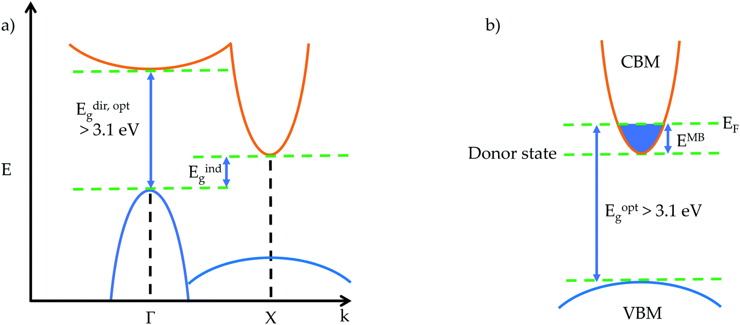 | ||
| Fig. 1 Simple schematics of (a) a band structure with an indirect fundamental gap and direct optical gap, and (b) the widening of the optical gap through the Moss-Burstein shift in an n-type transparent conductor. | ||
The optical gap is the energy of a transition measured from optical experimental techniques,14,15 and can be larger or smaller than the fundamental gap. From the perspective of a theorist, the optical gap is the first direct allowed transition, corresponding to the band gap observed experimentally. If there is an excitonic state within the band gap of a material, formed by the Coulombic attraction of an electron–hole pair, then an electron can be excited from the VBM to this lower energy state rather than the CBM, giving an optical gap that is smaller than the fundamental gap. Opposite behaviour can be observed when the transition from the VBM to CBM is forbidden due to Laporte selection rules. Forbidden transitions will experience very weak intensity, such as d–d transitions, whereas the first allowed transition will experience a strong absorption onset, causing the optical gap to be larger than the fundamental gap.16 Selection rules governing symmetry, parity and spin can all have an effect on determining the first allowed transition from occupied to unoccupied states, and the optical transition matrix can lend great insight into which transitions are allowed and forbidden.
Another phenomenon that can affect the magnitude of the optical band gap in transparent conductors is the Moss–Burstein shift, illustrated for an n-type transparent conductor in Fig. 1b. An electron donor will raise the Fermi level above the conduction band minimum, increasing the band gap by EMB – this is well established in CdO.17
Also important to transparency is the prevention of intra-band excitation. This means that for a p- (n-) type TCM, there should be an optical gap greater than 3.1 eV between the VBM (CBM) and the next occupied state below (unoccupied state above). This ensures that when charge carriers are added to the system in the form of defects, typically near or in the VBM (CBM), optical transitions to (from) these defect states from below (to above) still fulfil the transparency criteria.19
| σ = neμ, | (1) |
Charge carrier concentration is also intimately linked to transparency via the plasmon frequency ωp2 relationship, describing the oscillation of charge carriers within an applied field:
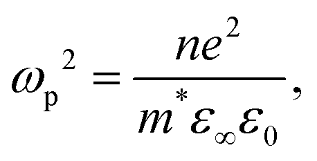 | (2) |
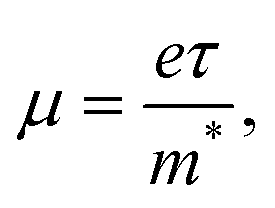
Charge carrier mobility μ is controlled by the equation:
 | (3) |
 | (4) |
 | (5) |
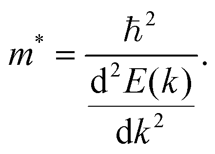
Qualitatively, the charge carrier effective mass can be assessed by the dispersion or curvature of the relevant band edge, with a greater curvature indicating a lower effective mass and therefore higher mobility.
The carrier lifetime is determined by scattering mechanisms concerning lattice phonons, charge carriers, grain boundaries and ionised impurities,21 and is therefore strongly dependent on the elements in the system, the crystal structure, and the quality of the sample, for example if it is a single crystal, thin film, pressed powder or has undergone nano-structuring.23
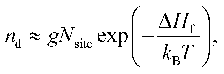
The concentration of a defect nd, and hence charge carriers, is ultimately determined by the free energy of formation, with the main component coming from enthalpy (vibrational entropy is assumed to be negligible here):
 | (6) |
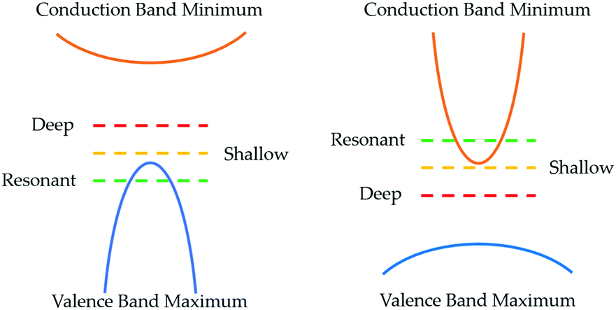 | ||
| Fig. 2 Defect classifications in p- and n-type TCMs (left and right respectively). | ||
For a more thorough discussion on the calculation of defects in crystalline systems and implementations of the necessary corrections for ab initio calculations, the reader is directed to the discussions by Lany and Zunger,32,33 Freysoldt et al.,34 Kumagai et al.,35,36 and Walsh.27
2.2 Sustainability requirements
In addition to the stringent electronic requirements of TCMs, there are other a handful of other factors to be considered when designing a new material. It will ideally consist of cheap, non-toxic, earth abundant elements to enable a secure, safe and sustainable manufacturing process. While ITO is a highly successful n-type TCM, the unstable supply and often wildly fluctuating price of raw indium is of concern,37 feeding research efforts into seriously optimising existing indium-based technologies and developing indium-free alternatives.28,38 Furthermore, synthesis should be straightforward, easily scalable to provide incentive for industrial investment, the material will ideally integrate well into existing device infrastructures, have excellent air and moisture stability and long-term durability. A comprehensive overview of p-type TCM device design and performance, including thin film transistors and complementary metal oxide semiconductor devices, can be found in the work by Wang et al.53 Prototypical p-type TCMs
3.1 Chemical modulation of the valence band
The first p-type TCMs were designed around the electronic structure of the n-type transparent conducting oxides (TCOs). In n-type TCOs such as In2O3, SnO2 and ZnO, the valence band is dominated by O 2p electronic states that display highly localised behaviour due to the large electronegativity of oxygen atoms.28,29,39 To engineer a p-type TCO, the localisation of the valence band needs to be modified such that holes can conduct throughout the material rather than being localised around the oxygen atoms. This can be done by introducing a closed shell cationic species with similar energy levels to O 2p states to facilitate the sharing of electron density, and for this they identified Cu+ with electronic configuration 3d104s0. The crystal structure also plays an important role, with materials that enable maximum spatial overlap between Cu and O atoms achieving the greatest degree of covalency and in turn giving the most disperse valence band maxima, while maximising the distance between Cu atoms to prevent inter-band d–d transitions that could cause colourations and bring down the energy of the conduction band states.40 These strategies were pioneered by Kawazoe et al.41 and have formed the basis of two decades of p-type TCM research.3.2 Delafossites
The delafossite CuAlO2 is the prototypical p-type TCO, highlighted as an exemplar material in the design strategies outlined by Kawazoe et al. It has an optical band gap of 3.5 eV and p-type conductivity of around 1 S cm−1 when nominally undoped.41 The crystal structure, shown in Fig. 3, consists of linear Cu–O–Al–O–Cu linkages, facilitating excellent spatial overlap between Cu and O atoms. Density functional theory (DFT) calculations using the hybrid functional HSE06 reveal an indirect band gap of 3.52 eV, matching well with the optical gaps reported in experiment, and good dispersion in the Γ → F direction. Defect calculations have shown that the lowest energy p-type defects in CuAlO2 are Cu on Al substitutions (CuAl) and copper vacancies (VCu), which both contribute to the modest conductivity measured at room temperature,31 although both of these defect states are deep acceptors. The holes generated by VCu are localised on the 6 surrounding Cu atoms, while there is a small distortion of the O–Cu–O dumbbell, indicative of a “reasonably localised polaron”. A small activation energy is required for the holes to overcome this interaction and migrate through the system, which places an intrinsic limit on the conductivity.31 While CuAlO2 itself is not a high performance p-type TCM, it is the first TCM and embodies the design principles set out by Kawazoe et al., kick-starting the research drive for Cu-based transparent conductors.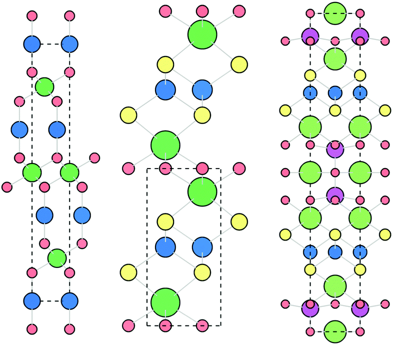 | ||
| Fig. 3 The rhombohedral delafossite (left, CuMO2, Cu = blue, M = green, O = red), quaternary oxychalcogenide (centre, LnCuOCh, Ln = green, Cu = blue, O = red, Ch = yellow) and quinary oxychalcogenide (right, (Cu2S2)(A3M2O5), Cu = blue, Ch = yellow, A = green, M = pink, O = red, see Section 4.6) crystal structures. Viewed along c axis, visualised using VESTA.56 | ||
Substitution of the M3+ cation in the delafossite structure has been widely investigated in order to further reduce the localisation of the valence band and enable greater p-type conductivity. Cr,42–46 Sc,47 Y,47 Ga,48,49 and In have all been studied,50 with CuCrO2 achieving the best performance – p-type conductivity of 278 S cm−1 and an optical gap of 3.52 eV when co-doped as Mg:N–CuCrO2.45 This is due to the large degree of covalency that is achieved in Cu–O–Cr–O–Cu linkages compared to the other M3+ cations, demonstrated through Bader charge analysis and partial electronic density of states calculations. Indeed, the charge transfer decreases in the order Cr, Sc, Y, Al, correlating with the reported experimental conductivities.51 This increased charge transfer has been observed separately using DFT in a series of CuAl1−xCrxO2 compounds, and distinct changes in the valence band are observed in X-ray photoelectron spectroscopy measurements of CuAlO2 and CuCrO2.42,52
Defect studies of CuCrO2 have shown that the formation energy of substitutional MgCr is around 0.9 eV lower than VCu, explaining the improved conductivity upon introduction of Mg.43 The interstitial oxygen defect Oi is also 1.5 eV lower in energy in CuCrO2 compared to CuAlO2, as the larger ionic radius of Cr generates more space in the structure, improving conductivity. It is suggested that NO incorporation also generates charge carriers,44 lowering the Fermi level and widening the band gap through a p-type Moss–Burstein shift, explaining the increased transparency compared to undoped films.45,46 The optical band gaps of CuGaO2 and CuInO2 are larger still, at 3.60 eV and 3.90 eV respectively.48–50 Due to its favourable band edge positions, CuInO2 is capable of bipolar doping,49,50 but conductivity in both of these compounds still remains several orders of magnitude behind CuCrO2.
A study by Huda et al. rationalises the band gap trends for the group III delafossites.49 For CuAlO2, CuGaO2 and CuInO2 (group IIIa delafossites crystallising in the rhombohedral structure shown in Fig. 3), the fundamental band gaps are indirect and decrease down the group, but the optical gaps increase. This can be explained by the nature of the conduction band states at Γ, which are comprised of M s states – moving from Al to Ga to In, these states lower in energy, decreasing the fundamental band gap. Meanwhile, the conduction band states that correspond to the direct transition (metal p states) are, relatively, shallower, causing a slight rise in energy and explaining the increase in optical gaps. In the group IIIb delafossites (Sc, Y and La, which crystallise in the slightly difference hexagonal delafossite structure), the metal s states at the Γ point in the conduction band are not nearly as deep, and instead the partially filled, lower energy d orbitals control the behaviour of the conduction band. Moving from Sc to Y to La sees a smaller relative change in the energy of the d states than moving from Al to Ga to In does in their s states, hence the difference in the fundamental and optical gaps is less pronounced in the group IIIb delafossites.49
SrCu2O2 crystallises in a delafossite related structure (tetragonal I41/amd, with trademark linear O–Cu–O dumbbell bonds among distorted SrO6 octahedra), allowing good spatial overlap between Cu and O atoms. It has an optical gap of 3.3 eV from experiment due to direct transitions, in qualitative agreement with GGA calculations (a direct gap but with a smaller value of 2.1 eV due to the band gap under-estimation inherent in GGA DFT).53 This is in contrast with most delafossites which have an indirect band gap. Conductivity originates from a thermally activated polaronic hopping mechanism, as in CuAlO2 and CuCrO2, with cationic vacancies VCu and VSr having formation energies of around 1 eV each. Conductivity fails to surpass 10−2 S cm−1, even when extrinsically doped with Ca or K,53–55 precluding SrCu2O2 from becoming a high performance material.
The delafossites are an important family of materials, and certainly deserve their place in the archives as the “original blueprint” for p-type TCM design. They benefit from relatively straightforward deposition and wide optical gaps, but are inherently flawed due to the deep acceptor levels present and subsequent polaronic conductivity mechanisms.
3.3 Oxychalcogenides
With the general formula LnCuOCh (Ln = La, Y, Pr, Nd, etc. and Ch = S, Se, Te), Cu-oxychalcogenides possess a structural motif that enables p-type conductivity and optical transparency (Fig. 3). With alternating layers of [Ln2O2]2+ and [Cu2Ch2]2−, oxychalcogenides combine the wide band gap properties of metal oxides with the excellent orbital mixing of Cu d and Ch p states, while maintaining a spatial separation between the two sub-structures. This allows for high hole mobility, as the oxygen 2p states are spatially and energetically separated from the valence band orbitals of the [Cu2Ch2]2− layers.The first oxychalcogenide p-type transparent conductor was LaCuOS,57 with an optical band gap of 3.1 eV and conductivity of around 20 S cm−1 upon Sr-doping.58,59 The highly electropositive La raises the energy of the conduction states, giving a wide band gap, while holes generated by Cu vacancies are confined to the conduction pathways in the Cu–S layers.57
Oxychalcogenides offer a rich search space for new TCs as they are open to a large variation in chemical composition. By varying the Ln site from La to Pr to Nd (in LnCuOS), the optical band gap changes from 3.14 eV to 3.03 eV to 2.98 eV. This is due to the lanthanide contraction, decreasing bond lengths in the a-axis, altering the Cu–Cu bond distance, increasing Cu 4s antibonding state interaction in the conduction band and lowering the band gap.60 Altering the Ch anion from S to Se to Te (across LaCuOCh) also sees a decrease in the band gap from 3.14 eV to 2.80 eV to 2.40 eV, but not because of the change in ionic radii. Instead, the relative energy of the Ch orbital at the valence band increases, closing the band gap. The overlap between Cu 3d and Ch np improves as the Ch gets larger, resulting in improved hole mobility down the group.60,61
Of these variations, LaCuOSe has been widely studied due to its high p-type conductivity, achieving 910 S cm−1 at carrier concentrations of 1021 cm−3 when doped with Mg.62 This level of conductivity is competitive with n-type oxides, but with an optical band gap of 2.8 eV LaCuOSe is not fully transparent. Hybrid DFT calculations place the formation energy of VCu at around 1.5 eV under Cu-poor growth conditions, and the transition level occurs around 0.1 eV above the VBM hence the high conductivity. The MgLa defect occurs at a slightly higher formation energy of 2.4 eV, but it is proposed that Sr and Ca can act as low energy acceptors that could improve the conductivity even further.63 However, optical transitions from the VCu defect prevent a Moss–Burstein shift that would open up the band gap, so the transparency of LaCuOSe is permanently compromised.
The mixed cation system (La1−xYxCuOS) (with x = 0 → 0.25) holds the record for the highest experimental conductivity of an oxychalcogenide with a band gap greater than 3 eV – 89.3 S cm−1 and 3.06 eV respectively.64 XPS and ICP (inductive coupled plasma) compositional analysis reveals a 14% Cu deficiency, suggesting that VCu is responsible for the conductivity. This is likely true in light of the defect landscape of pure LaCuOS, where VCu formation is favourable. The best films are highly crystalline, but are still orders of magnitude smaller than the required levels of conductivity for high performance TCs.
3.4 Oxides
As well as ternary and quaternary oxides, a handful of binary oxides have influenced the direction of p-type TC research, and deserve an honourable mention. Cuprous oxide, Cu2O, has an exemplar valence band for p-type TCMs, where the Cu 3d and O 2p orbitals interact to such an extent that hole mobility of 256 cm2 V−1 s−1 has been observed experimentally.65 However, Cu atoms are closer together in Cu2O than in the CuAlO2 crystal structure, giving greater overlap between Cu 4s states in the conduction band, bringing the energy down and ultimately reducing the fundamental band gap to 2.17 eV.66 A disallowed transition from VBM to CBM results in an optical gap of 2.5 eV, but this still falls short of the transparency requirement, and deep acceptor levels are also a disadvantage, imposing an upper limit on achievable conductivity.66 Nonetheless, Cu2O has seen resonable success, certainly as a proof-of-concept, as a p-type thin-film transistor (TFT).67Cr2O3 is an antiferromagnetic insulator with an optical band gap of around 3.4 eV.68 Strong electron correlation in Cr2O3 results in a conduction band of 3d character, while the valence band is made up of Cr 3d and O 2p orbitals. This electronic structure allows p-type doping, capable of reaching conductivity of 28 S cm−1 when doped with Ni.69 DFT calculations show that Mg-doping is also possible with relatively low formation energy (0.9 eV), however the acceptor level is quite deep, so conductivity levels are unlikely to surpass that of Ni-doped Cr2O3.70
SnO is a curious transparent conductor with a fundamental indirect band gap of 0.7 eV but an optical band gap of 2.6 eV (Fig. 4), resulting in thin films that display a yellow hue.18 Films deposited by magnetron sputtering are capable of reaching a maximum hole mobility of 18.7 cm2 V−1 s−1 at carrier concentrations of 2.2 × 102 cm−3.71 However, the most interesting feature of SnO is that it can act as a bipolar transparent conductor and form a homogeneous p–n junction.72 This is precisely due to the nature of the band structure and the forbidden fundamental band gap, with the relatively high energy valence band states resulting in a small ionisation potential that is conducive to p-type conductivity, and the relatively low energy conduction band states resulting in a large electron affinity that allows n-type conductivity, all while remaining (semi-)transparent.18 SnO remains an interesting candidate for bipolar transparent semiconductors, but the yellowish tint, as well as the undesirable tendency to oxidise to SnO2, pose significant obstacles to its widespread application.
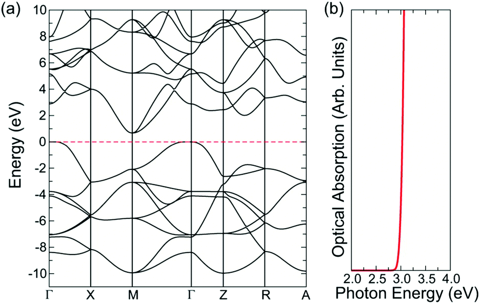 | ||
| Fig. 4 Band structure and optical absorption spectrum of SnO, calculated with the PBE0-vdW functional. Reprinted with permission from Quackenbush et al.18 Copyright 2021 American Chemical Society. | ||
NiO is a popular p-type semiconductor with a large optical band gap, often reported in excess of 3.4 eV, and with transmissivity in the range of 60–90% depending on film deposition method.6,73–75 Conductivity is modest at best, with several experimental reports failing to synthesise films surpassing 10 S cm−1,74,75 although hole mobility of around 28 cm2 V−1 s−1 has been achieved through oxygen assisted sputtering (at the cost of transparency). Doping the Ni site with various alkali metals, in particular Li, has been reported to improve conductivity.76,77 However, a consistent theoretical model has yet to be agreed upon, with further work required to understand the nature of the hole localisation in both doped and non-doped NiO.11,78 While the electronic properties of NiO are not ground-breaking, it is an incredibly attractive TCM due to its simple rock-salt structure.79 This allows it to interface straightforwardly with other cubic materials, such as successful n-type transparent conductors like Sn-doped In2O3, leading to major efficiency gains in perovskite solar devices as an interfacial anode layer,73 and as a result is one of the most widely implemented commercial p-type transparent electrodes.6
4 Emerging p-type TCMs
4.1 Materials screening
High throughput computational screening has been an invaluable tool in the search for new p-type TCMs. Databases containing thousands of crystal structures and electronic structure data (for example the Materials Project)99 can be queried with sophisticated search parameters, assessing swathes of materials for potential p-type TCM properties. Brunin et al. provide a thorough overview and explanation of the processes involved, discussing each stage of the search funnel,26 and an assessment of how well high throughput descriptors actually perform can be found by Woods-Robinson et al.100 The quality of the data in such databases is ultimately the limiting factor in the efficacy of the screening process – for example, older entries in crystallographic databases may not have been verified for any number of decades. For electronic structure databases, it is simply not possible to assess every single entry at a high level of theory – in fact, most entries are computed with GGA exchange correlation functionals, well known to underestimate band gaps and perform poorly for certain systems, so results from screening will often need to be validated by further independent research, and screening parameters themselves will often have to be compromised to include results that would otherwise be screened out (for example, if searching by GGA band gap, one might choose a minimum of 1 eV rather than 3 eV as GGA band gaps are underestimated by around 50%). The focus of this section will be on innovative directions in p-type TCM research, with many of the materials featured having been discovered in high throughput screening studies.4.2 d6 Spinel oxides
The electronic configuration of the Cu(I) ion, 3d10, is well suited for mixing with oxygen 2p states and increasing the dispersion of the valence band, but there are other “quasi-closed shell” configurations that can also act as a solid foundation for p-type oxides. The d6 spinel oxides are excellent examples of this, where for low spin systems in an octahedral field they are essentially closed shell (the three t2g orbitals are fully occupied). The filled metal t2g orbitals interact with the O 2p states at the VBM, while the unoccupied eg states contribute to the conduction band, similar to the splitting of the d orbitals in antiferromagnetic Cr2O3.68 ZnM2O4 (M = Co, Rh, Ir) have indirect band gaps of 3.96 eV, 2.88 eV and 2.37 eV respectively, calculated with the HSE06 functional,84 and relatively low formation energy of the ZnM defect is reported for each system. The Co variant is the most studied experimentally, achieving conductivity levels of 21 S cm−1, and can also be doped n-type to deposit a p–n heterojunction.6,101 While an intuitive example of materials design, it is unlikely that the d6 spinels will achieve record performances as the valence bands remain quite flat, and conductivity originates from a polaronic hopping mechanism. Furthermore, there have been conflicting experimental reports regarding the trends in conductivity and band gaps in these systems,6,83 indicating that further understanding is required.4.3 p-Type perovskites – the next generation?
Sr-doped LaCrO3 is another take on the quasi-closed shell configuration design strategy, where half-filled t2g orbitals comprise the valence band. A forbidden transition from t32g → e0g (2.8 eV) opens up the next available transition as the optical gap at 4.6 eV, resulting in excellent levels of transparency.85 Doping to 50% Sr on the La site, arguably now forming a mixed cation perovskite, results in conductivity of 50 S cm−1, but at the cost of a 50% loss in transmission. Despite this, Sr-doped LaCrO3 remains of interest due to its perovskite structure, which could interface well with other perovskite based TCMs, such as n-type La-doped BaSnO3.The rhombohedral double perovskite Ba2BiTaO6 was identified through a high throughput screening study as a wide band gap oxide with good hole mobility.26,86 The filled Bi 6s2 valence shell hybridises with the O 2p states at the VBM, while the Ta forms high energy conduction band states to ensure a large band gap of around 3.6 eV calculated with hybrid DFT (3.8 eV with GW theory), although from experiment this is even larger at 4.5 eV.86 When doped with K on the Ba site, Ba2BiTaO6 displayed hole mobility of 30 cm2 V−1 s−1, but extremely low carrier concentration (1014 cm−3) and therefore low conductivity. This is due to the charge compensating n-type defects that form, such as VO and TaBi,87 which ultimately prevent Ba2BiTaO6 from achieving competitive levels of conductivity.
Doping with K onto Ba sites has also been reported in the traditionally n-type material BaSnO3.88 A heterojunction was created with p-type K-doped and n-type La-doped BaSnO3, demonstrating stability after high bias and thermal cycling. The p-type films displayed mobility of 0.30 cm2 V−1 s−1 at a carrier concentration of 1013 cm−3, giving low overall conductivity. An activation energy for K dopants is reported to be 0.5 eV, but there is no support from DFT calculations or theory otherwise at the time of writing.88 Given the low carrier concentration, it is likely that the intrinsic n-type defects in BaSnO3, such as oxygen vacancies, or even adventitious hydrogen, will dominate in this system even under cation-poor conditions,89 and high performance p-type activity is unfavourable.
Caesium based halide double perovskites, with the general formula Cs4M2+B23+XVII12 (M = Mg, Ca, Sr, Zn, Cd, and Sn(II), B = Sb, In and Bi, X = Cl, Br and I), have gained much interest in recent years as potential p-type TCMs, after a screening study identified 7 from a possible 54 elemental combinations that displayed thermodynamic stability, a band gap greater than 2.8 eV, a hole effective mass lighter than 1.2m0 and good intrinsic p-type conductivity.90 Cs4CdSb2Cl12 is chosen as the most promising candidate, with delocalised Sb 5s orbitals mixing with Cl p states at the VBM suggesting good p-type performance, and defect calculations predicting intrinsic conductivity as a result of shallow CdSb acceptor levels with low formation energy. However, Cs4CdSb2Cl12 and Cs4CdBi2Cl12 have been shown to be the only two of the predicted seven that are thermodynamically stable and synthesisable from a solvothermal method, and that they are in fact transparent insulators rather than conductors.91 Hybrid DFT calculations show that the band gap is around 3.3 eV, and that the valence band actually lies lower in energy than the initial GGA calculations from the previous study suggested. The initial GGA calculations therefore predicted unrealistically facile p-type doping. Furthermore, upon inclusion of all stable competing phases of Cs4CdSb2Cl12, it is found that the chemical potential limits alter the defect landscape significantly, to the point where CdSb is fully charge compensated by various native n-type defects, resulting in a hole concentration that is too far below the limit measurable for Hall techniques (Fig. 5).91 This quite firmly rules out caesium based halide double perovskites from becoming successful p-type TCMs, and demonstrates the importance of rigorously calculating chemical potential limits for defect analysis, as well as capturing an accurate description of band edges and gaps.
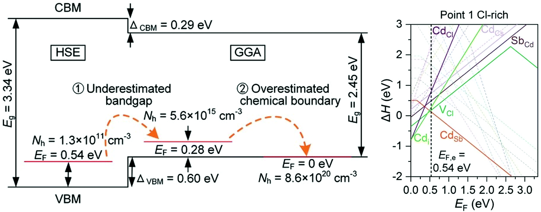 | ||
| Fig. 5 Schematic of HSE and GGA band gap calculations and effects of miscalculated chemical potentials (left), transition level diagram calculated with HSE under the most favourable p-type conditions, showing n-type charge compensation (right). Reprinted with permission from Hu et al.91 Copyright 2021 Advanced Functional Materials, John Wiley and Sons. | ||
A separate high throughput study highlighted another set of double halide perovskites, starting with over 16![[thin space (1/6-em)]](https://www.rsc.org/images/entities/char_2009.gif) 000 Cs- and Rb-based possible compounds, searching for thermodynamic stability, a GGA band gap greater than 1.8 eV and hole effective mass less than 1m0.102 They report 17 double perovskites, and one ternary perovskite CsPbF3, with (meta) stability and band gaps predicted to be greater than 3 eV with the hybrid functional HSE06, although 7 of these contain heavy and or toxic elements. This narrows the band gap upon consideration of relativistic effects (using spin orbit coupling calculations) and also renders them unsuitable for every day use. The relatively low hole effective masses in the remaining candidate materials, such as Rb2AgBiCl6 and Cs2InLaBr6 (0.49 and 0.59m0 respectively), are a result of halogen p and metal s states mixing well at the valence band. However the authors recognise that the ultimate obstacle for these materials is their p-type dopability, which in this case has not been studied computationally, and there is a call to arms for experimental investigation.102 Hu et al. have already demonstrated that it is not possible to generate sufficient p-type carriers in Cs4CdSb2Cl12 due to the spontaneous formation of native n-type defects,91 which could be the downfall of these Cs and Rb double halide perovskites too.
000 Cs- and Rb-based possible compounds, searching for thermodynamic stability, a GGA band gap greater than 1.8 eV and hole effective mass less than 1m0.102 They report 17 double perovskites, and one ternary perovskite CsPbF3, with (meta) stability and band gaps predicted to be greater than 3 eV with the hybrid functional HSE06, although 7 of these contain heavy and or toxic elements. This narrows the band gap upon consideration of relativistic effects (using spin orbit coupling calculations) and also renders them unsuitable for every day use. The relatively low hole effective masses in the remaining candidate materials, such as Rb2AgBiCl6 and Cs2InLaBr6 (0.49 and 0.59m0 respectively), are a result of halogen p and metal s states mixing well at the valence band. However the authors recognise that the ultimate obstacle for these materials is their p-type dopability, which in this case has not been studied computationally, and there is a call to arms for experimental investigation.102 Hu et al. have already demonstrated that it is not possible to generate sufficient p-type carriers in Cs4CdSb2Cl12 due to the spontaneous formation of native n-type defects,91 which could be the downfall of these Cs and Rb double halide perovskites too.
4.4 Binary oxides
Achieving p-type doping in materials such as In2O3, SnO2 and ZnO has been a goal of materials researchers for decades, as this would enable an efficient homogeneous p–n junction and seamless integration with existing device architecture. Indeed, there have been occasional experimental reports of p-type conductivity in native n-type materials,88,103–107 but these results are often transient and difficult to reproduce. This is because these post-transition metal oxides are natively n-type, with “hole-killing” defects forming under all synthesis conditions. Multiple hybrid DFT studies have gone on to prove this quantitatively, showing that the formation of acceptor defects in these materials is thermodynamically unstable.28,30,89,108–111 One possible strategy for achieving p-type conductivity in such systems is to significantly alter the make-up of the valence band, for example through mixed cation alloying.With an ultra-wide band gap of 4.9 eV,112–114 Ga2O3 is a prospective material for the power electronics industry due to its large breakdown voltage and improved band gap over rival materials GaN and SiC. Significant alloying of Ga2O3 with Bi2O3 is a promising route to engineering p-type behaviour in this natively n-type system.115 The formation of an intermediary valence band of Bi s character at around 1.6 eV above the valence band of the host material allows mixing with oxygen 2p states to improve band dispersion, while maintaining optical transparency.115 Mg, Zn and Cu are investigated as potential extrinsic dopants in both Ga2O3 and the Bi–Ga2O3 alloy, with MgGa and ZnGa calculated to have relatively low formation energies, but deep transition levels. This is due to the wavefunction of the acceptor state coupling to the localised hole state on an oxygen in the valence band, regardless of the position of the valence band. The CuGa defect does not couple to a valence band oxygen, and so even though it is a deep acceptor in Ga2O3, it is shallow in the alloyed system now that the valence band has shifted up in energy, and the holes are localised on the Cu impurity site.115 This is an intriguing new approach to engineering dispersion and acceptor levels, and such alloying could be applied to other materials with strongly correlated valence (or indeed conduction) bands. However, the localisation of the holes around the Cu defect site suggests that mobility may still not reach the levels required for use on a commercial scale.
β-TeO2 has been recently proposed as a wide band gap semiconductor due to its direct band gap of 3.70 eV in monolayer form.92,116 Hybrid DFT calculations show that the valence band is comprised mainly of Te 5p and O 2p, with smaller contributions from Te 5s orbitals, and that there is high, anisotropic mobility of both electrons and holes, with the latter predicted to reach mobility of 9100 cm2 V−1 s−1 in the Γ → X direction for the monolayer system.116 It was calculated to have a low cleavage energy similar to black phosphorus, so exfoliation is expected to be relatively straightforward. Indeed, synthesis of β-TeO2 bilayers has been successful from a eutectic melt (Te:Se 5%:95%) droplet that is rolled on a silicon wafer using a van der Waals printing process.92 Both EELS and XPS measurement of the valence band confirmed a band gap of 3.7 eV, the hole effective mass was determined to be 0.51m0 from scanning tunnelling spectroscopy data, in good agreement with the theoretical value, and the bilayers performed well when deposited in field effect transistors. DFT calculations on the bilayer reveal hole mobility values of 436 cm2 and 7690 V−1 s−1 in the a and b directions respectively, due to the different conduction pathways on these axes. Hall measurements of the mobility gave an average value of 141 cm2 V−1 s−1.92 The p-type dopability remains to be tested, with the possibility of charge compensating native defects posing the biggest challenge, and there is of course the problem of Te abundance, but if a large hole concentration can be engineered in β-TeO2 then it could be an exciting direction for future research.
4.5 Beyond oxides for valence band dispersion
An alternative approach to engineering a dispersive valence band is to move away from oxides and instead encourage cation orbital mixing with the 3p states of phosphorus. With a higher principal quantum number, phosphorus valence orbitals are more diffuse than those of oxygen. Ternary phosphides MCuP where M = Mg, Ca, Sr and Ba have been investigated using hybrid DFT, with excellent mixing of Cu 3d and P 3p states reported for each compound (42:54 for MgCuP and 38(9):48 for CaCuP, SrCuP and BaCuP) resulting in extremely low hole effective masses in the a and b directions for the trigonal planar coordinated Cu–P systems CaCuP, SrCuP and BaCuP.93 This is another example of how the synergistic crystal-electronic structure relationship is key for engineering p-type TCMs – the smaller ionic radius of Mg forces the Cu in MgCuP to adopt a tetrahedral coordination environment, which has poorer overlap with the P 3p orbitals resulting in a less disperse VBM, compared to the trigonal planar arrangement in the other three systems due to their larger group II cations. Conductivity of pressed powder samples of CaCuP indicate intrinsic p-type conductivity, and optical measurements indicate a strong absorption onset at around 2.8 eV, in good agreement with theory –93 thin films or single crystals are likely to display higher levels of conductivity and mobility, with Cu vacancies likely responsible for the intrinsic conductivity. While not completely transparent, the ternary phosphides certainly teach us valuable design principles for engineering valence band dispersion.
Boron phosphide (BP) is the product of another high throughput screening process, where the search space was expanded from oxides to include sulfides, nitrides and phosphides. Indeed, the authors found that of the 30000 compounds screened, phosphides had on average the lowest hole effective mass, but also the lowest band gaps.94 However, for BP this is not an issue, as even though the indirect gap is quite small (2.26 eV with the HSE06 functional and 32% HF exchange) it possesses a much larger direct gap of around 4 eV, easily surpassing the transparency requirement. It is found that AlP also displays this behaviour, but the hole effective mass in BP is significantly lower and is the most promising candidate that emerged from this screening process. A separate study, using electron–phonon coupling calculations, predicts hole mobility as high as 900 cm2 V−1 s−1.95 The good overlap of B 2p and P 3p orbitals gives rise to the disperse valence bands, while the relative energies of the group III cation s states control the magnitude (and type) of the gap – in BP the s antibonding states are much higher in energy, resulting in the direct transition at Γ occurring between p bonding and antibonding states, whereas with Al the s antibonding states are slightly lower, causing a smaller direct band gap, and in Ga and In the s antibonding states are actually lower in energy than the p antibonding states, causing the fundamental gap to become direct and transparency unachievable.94 There are no low energy “hole killer” defects in BP, and it is suggested that substitutional BeB would be an excellent acceptor defect, with low formation energy and no self compensation. Experimental reports of BP are relatively sparse, with the best conductivity and hole concentration measured in the 1970s (2800 S cm−1 and 1 × 1019 cm−3),96 deposited in a hydrogen rich atmosphere and subsequently annealed. In ZnO, it is reported that sample growth in hydrogenic conditions can facilitate the formation of low energy hydrogen-defect complexes – subsequent annealing removes the hydrogen, but the low energy defects remain, giving excellent conductivity.117 It is possible that a similar mechanism is possible in BP, not accounted for in the defect study by Varley et al.94 BP has also been extensively researched as a hardening coating for military aircraft windshields, evidence that it is sufficiently transparent and relatively straightforward to synthesise on a large scale.118 However, there have been few reports of high quality single crystals grown in recent years, indicating that synthesis challenges may still remain for p-type TCM applications.
Cuprous iodide was first documented as a transparent conductor over 100 years ago, when Bädeker iodised metallic copper films in iodine vapour, forming layers of transparent CuI.119 Today, film synthesis is still straightforward, with the direct evaporation of CuI powder onto glass substrates a popular deposition technique.10 With a direct band gap of around 3.1 eV, it is comfortably transparent, and has relatively disperse valence bands formed of I 5p and Cu 3d states giving rise to a hole effective mass of roughly 0.30m0, indicating high mobility and conductivity.97 The best mobility of thin films of CuI is 43.9 cm2 V−1 s−1,120 but growing epitaxial single crystals of CuI has been challenging despite the long history of the material. Recently, molecular beam epitaxy growth of single crystal CuI on sapphire and Si substrates has been reported, displaying average hole concentration and mobility of 5.47 × 1017 cm−3 and 45 cm2 V−1 s−1.80 Photoluminescence spectra indicate that CuI can emit light at an intensity one order of magnitude greater than GaN, finding possible use in LED applications, and temperature dependent measurements reveal what is suggested to be a Cu-vacancy related band, confirming previous DFT predictions that Cu vacancies are responsible for intrinsic conductivity.80,97 Generating a greater number of charge carriers is key to driving up conductivity in this material, but perhaps a more concerning issue is its poor air and moisture stability, especially at elevated temperatures, due to the ease with which Cu migration can occur.10
Non-oxide materials have been of great interest to researchers in recent years, as they lend themselves well to improving valence band dispersion. However, significant issues remain which question their suitability as the p-type TCMs of tomorrow. Air and moisture sensitivity are obvious issues that could prevent their widespread use, as well as the inclusion or release of toxic chemicals upon device breakdown (such as phosphorus), but that does not rule out non-oxides as useful materials for more niche applications where humans are unlikely to come into contact with the device. Despite the challenges that stability and toxicity may pose, great insight into future materials design has been gained from understanding the bonding in these systems.
4.6 Next generation quinary oxychalcogenides
The first generation of oxychalcogenides identified for p-type TCM applications had the general formula LnCuOCh – by switching out the binary oxide layer for a ternary oxide, an even greater variation in chemical composition is accessible (Fig. 6 shows this schematically). The first successful quinary oxychalcogenide was (Cu2S2)(Sr3Sc2O5), with a direct optical band gap of 3.1 eV, room temperature conductivity of 2.8 S cm−1, and an impressive hole mobility of 150 cm2 V−1 s−1,98 competitive with electron mobility in the highest performing n-type TCOs. Similar to the quaternary oxychalcogenides, the hole conductivity pathway is spatially separated from the oxygen containing layers, so the valence band is not made of O 2p character but instead between Cu 3d and S 3p states, enabling high hole mobility.121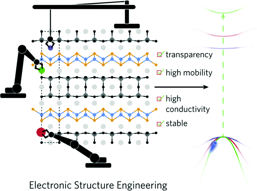 | ||
| Fig. 6 Exploring the chemical variations to the quinary oxychalcogenide structure. Reprinted with permission from Williamson et al.40 Copyright 2021, Elsevier Inc. | ||
A recent screening study of 24 variations to the (Cu2S2)(A3M2O5) structure where A = Sr, Ca, Ba, and Mg and M = Sc, Al, Ga, In, Y and La has identified three novel compounds with dynamic stability and optical transparency. (Cu2S2)(Ca3Al2O5) and (Cu2S2)(Ba3Sc2O5) have optical gaps of 3.17 eV and 3.24 eV respectively, suggesting complete optical transparency, while (Cu2S2)(Sr3Sc2O5) has an optical gap of 3.06 eV, on the border of transparency.40 Focussing on the CaAl and BaSc compounds, they possess light hole effective masses in the Γ → N direction of 0.37m0 and 0.43m0 respectively, indicative of extremely high hole mobility considering that (Cu2S2)(Sr3Sc2O5) displays mobility of 150 cm2 V−1 s−1 with a hole effective mass of 0.45m0. Predicted conductivities of the CaAl and BaSc compounds (from Boltzmann transport theory, assuming a hole concentration of 1021 cm−3) are 1767 and 2058 S cm−1, both exceeding the calculated value at this hole concentration for the parent compound (Cu2S2)(Sr3Sc2O5) of 1673 S cm−1, but these calculations assume high levels of p-type dopability. At a lower hole concentration of 1018 cm−3, the calculated conductivity for (Cu2S2)(Sr3Sc2O5) is 2.03 S cm−1, in reasonably good agreement with the experimental value of 2.8 S cm−1.98 Powder samples of the BaSc compound confirm the direct absorption onset at around 3.24 eV, although there is an absorption of lower intensity at around 2.26 eV, which could be from impurities or unwanted transitions (such as from defect states or Cu–Cu d transitions).40 Clearly these quinary oxysulfides show potential as p-type TCMs, but more extensive work is required – deposition as a thin film would allow for Hall measurements to be taken, quantifying the levels of conductivity and mobility, and a defect analysis would give an indication of the p-type dopability of these materials. However, one downside of these materials is their inherent structural complexity both for computationalists and experimentalists – the cost of performing a hybrid DFT defect study on a quinary system is extremely high, and the stability window of these systems may not be particularly large, especially when trying to grow under certain metal-poor conditions to encourage acceptor defect formation, such that phase pure films could be difficult to deposit.
5 An outlook on applications
A rich variety of inorganic materials have been presented in this review, covering many of the areas at the forefront of current research. This section will briefly discuss some of the current applications relying upon p-type TCMs, how these can be improved, and some of the challenges surrounding future device integration. For thorough and dedicated reviews on applications and devices the reader is directed to the works of Shi et al. and Wang et al.5,11For industrial applications such as laptop, phone and television displays, n-type transparent conductor LCD technology continues to dominate.11 With users desiring ever-improving resolution, electronic properties such as mobility and on–off ratio are absolutely vital, and p-type technology is several orders of magnitude behind systems such as amorphous indium–gallium–zinc–oxide (IGZO) thin-film transistors (TFTs).122 However, OLED displays are becoming increasingly popular, due to their improved contrast, lower power consumption, thinner display and wider viewing angle, and for these p-type TFTs are the preferential technology as they can simplify device architecture and improve efficiency.11,123
Of the materials discussed in this review, the binary oxides Cu2O, SnO and NiO have been most widely studied for p-type TFT applications. Despite being “the first” p-type TCO, CuAlO2 was only first deposited as a TFT in 2012, 15 years after its conception, with device mobility <1 cm2 V−1 s−1 and an on–off switching ratio of around 800 (several orders of magnitude behind IGZO).5,124 Cu2O can achieve the highest hole mobility, up to 256 cm2 V−1 s−1,65 but when implemented as a TFT the mobility fails to surpass 1 cm2 V−1 s−1 due to poor interfacing and grain boundaries.67 SnO also suffers from deposition problems, with SnO2 formation severely impacting the performance in TFT and complementary metal oxide semiconductor (CMOS) applications. NiO has the better chemical stability of the three, but suffers from low device mobility when implemented as a TFT, likely due to the localised holes generated by acceptor defects.11,78 NiO has however been met with success when integrated into perovskite solar cells as an interfacial anode layer, improving power conversion efficiency by acting as a hole-transport layer.73 Establishing improved deposition processes to nullify or contain the effects of grain boundary scattering and chemical instability is necessary to drive these oxides forward.
Implementation of materials with greater valence band dispersion is the next logical step in p-type TFT performance testing (for example CuI)125 in order to improve device mobility, but the greatest challenges are successful deposition and chemical stability. The quasi-two-dimensional layered materials discussed in this review, such as β-TeO2 and the oxychalcogenides for example, are perhaps less attractive than the three-dimensional or cubic crystal structures belonging to materials such as BP and NiO, due to charge transport being restricted to only two directions – this will create extra challenges for device integration. In the meantime, continued use of oxide p-type TCMs as hole transport (and electron blocking) layers to improve power conversion efficiency and overall performance is their most reliable application, while a ground-breaking, n-type matching material is awaiting discovery.
6 Conclusions
In this review, the fundamental design principles for p-type transparent conductors were outlined, the chief stratum of which is to delocalise electron density away from single elemental species and encourage orbital mixing to form a disperse valence band. This is in line with the notion of “chemical modulation of the valence band” first suggested for p-type oxides by Kawazoe et al.,41 but in recent years has been extended to include anions such as phosphides and halides.93,120 The discovery of new materials with potential p-type TCM properties has been turbo-charged with the advent of large scale database screening, an approach that is likely to spearhead efforts in discovering p-type TCMs in the years to come. Indeed, an increasing number of studies concerning the discovery of new battery and solar cell materials are making use of wide-scale database screening.126–128 Searching beyond known compounds in databases, noted by Walsh and Park,129 and into unchartered territory may reveal new directions for p-type TCM research – success has already been seen in the photovoltaics field, where machine-learning models have been able to predict chemical compositions that will produce band gaps suitable for solar energy applications using only earth abundant materials.130 However, the results from such large-scale screening studies will only ever be as reliable as the databases upon which they are built, and also often return complicated quaternary and quinary crystal structures, which pose significant challenges for theorists and experimentalists alike.Of the most interest in recent years are the significant developments made in the non-oxide field, with excellent valence band dispersion achievable in phosphides, selenides, tellurides and halides.63,80,92,94,116,120 Many of these materials have 3-dimensional crystal structures, in the sense that their conduction pathways exist in all three cartesian directions, such as BP due to its zinc blende structure, which is a significant advantage over the quasi-2-dimensional structures of delafossites and oxychalcogenides when implementing them into a heterojunction device. Overcoming stability, deposition and safety concerns in these simple non-oxide systems is a major goal in the coming years, as the allure of straightforward interfacing and potentially cheap synthesis of these basic crystal structures is attractive to industry – indeed, CuI has already generated interest as a p-type TFT.125 For applications where cost is irrelevant, more complex or non-earth abundant materials are likely to dominate. Significant challenges remain for most of the systems discussed in Section 4, with the majority only in their infancy, but these emerging materials mean the future looks bright for p-type TCM research.
Author contributions
J. W. conceptualised, wrote and prepared the manuscript with guidance from DOS.Conflicts of interest
There are no conflicts to declare.Acknowledgements
JW and DOS acknowledge Diamond Light Source for co-sponsorship of an EngD studentship on the EPSRC Centre for Doctoral Training in Molecular Modelling and Materials Science (EP/L015862/1). DOS acknowledges support for EPSRC (Grant number EP/N01572X/1). JW acknowledges useful discussions with A. Regoutz and T.-L. Lee, and is grateful for their mentorship. DOS acknowledges many useful discussions with G. W. Watson, R. G. Egdell, T. D. Veal, P. D. C. King, K. E. Smith, B. J. Morgan, A. Walsh, E. Arca, S. Lany and J. B. Varley.References
- C. G. Granqvist and A. Hultåker, Thin Solid Films, 2002, 411, 1–5 CrossRef CAS.
- N. Noor and I. P. Parkin, J. Mater. Chem. C, 2013, 1, 984–996 RSC.
- Transparent Electronics Market – Growth, Trends and Forecast (2020–2025), 2020, https://www.mordorintelligence.com/industry-reports/transparent-electronics-market.
- J.-Y. Kwon, D.-J. Lee and K.-B. Kim, Electron. Mater. Lett., 2011, 7, 1–11 CrossRef CAS.
- Z. Wang, P. K. Nayak, J. A. Caraveo-Frescas and H. N. Alshareef, Adv. Mater., 2016, 28, 3831–3892 CrossRef CAS PubMed.
- K. H. L. Zhang, K. Xi, M. G. Blamire and R. G. Egdell, J. Phys.: Condens. Matter, 2016, 28, 383002 CrossRef PubMed.
- N. Zhang, J. Sun and H. Gong, Coatings, 2019, 9, 137 CrossRef.
- R. Cao, H.-X. Deng and J.-W. Luo, ACS Appl. Mater. Interfaces, 2019, 11, 24837–24849 CrossRef CAS PubMed.
- L. Hu, R. H. Wei, X. W. Tang, W. J. Lu, X. B. Zhu and Y. P. Sun, J. Appl. Phys., 2020, 128, 140902 CrossRef CAS.
- A. N. Fioretti and M. Morales-Masis, J. Photonics Energy, 2020, 10, 1 Search PubMed.
- J. Shi, J. Zhang, L. Yang, M. Qu, D.-C. Qi and K. H. L. Zhang, Adv. Mater., 2021, 2006230 CrossRef CAS PubMed.
- O. Ostroverkhova, Chem. Rev., 2016, 116, 13279–13412 CrossRef CAS PubMed.
- H. B. Lee, W.-Y. Jin, M. M. Ovhal, N. Kumar and J.-W. Kang, J. Mater. Chem. C, 2019, 7, 1087–1110 RSC.
- J. Tauc, Mater. Res. Bull., 1968, 3, 37–46 CrossRef CAS.
- A. Dolgonos, T. O. Mason and K. R. Poeppelmeier, J. Solid State Chem., 2016, 240, 43–48 CrossRef CAS.
- A. Walsh, J. L. F. Da Silva, S.-H. Wei, C. Körber, A. Klein, L. F. J. Piper, A. DeMasi, K. E. Smith, G. Panaccione, P. Torelli, D. J. Payne, A. Bourlange and R. G. Egdell, Phys. Rev. Lett., 2008, 100, 167402 CrossRef PubMed.
- M. Burbano, D. O. Scanlon and G. W. Watson, J. Am. Chem. Soc., 2011, 133, 15065–15072 CrossRef CAS PubMed.
- N. F. Quackenbush, J. P. Allen, D. O. Scanlon, S. Sallis, J. A. Hewlett, A. S. Nandur, B. Chen, K. E. Smith, C. Weiland, D. A. Fischer, J. C. Woicik, B. E. White, G. W. Watson and L. F. J. Piper, Chem. Mater., 2013, 25, 3114–3123 CrossRef CAS.
- Ç. Klç and A. Zunger, Phys. Rev. Lett., 2002, 88, 095501 CrossRef PubMed.
- N. Preissler, O. Bierwagen, A. T. Ramu and J. S. Speck, Phys. Rev. B: Condens. Matter Mater. Phys., 2013, 88, 085303 CrossRef.
- A. M. Ganose, J. Park, A. Faghaninia, R. Woods-Robinson, K. A. Persson and A. Jain, Nat. Commun., 2021, 12, 2222 CrossRef CAS PubMed.
- S. Majdi, V. Djurberg, N. Suntornwipat, M. Gabrysch and J. Isberg, Adv. Theory Simul., 2020, 4, 2000103 CrossRef.
- G. S. Nolas, J. Sharp and H. J. Goldsmid, Thermoelectrics, Springer Berlin Heidelberg, 2001, pp. 177–207 Search PubMed.
- W. Mönch, Appl. Surf. Sci., 1997, 117-118, 380–387 CrossRef.
- A. Schleife, F. Fuchs, C. Rödl, J. Furthmüller and F. Bechstedt, Appl. Phys. Lett., 2009, 94, 012104 CrossRef.
- G. Brunin, F. Ricci, V.-A. Ha, G.-M. Rignanese and G. Hautier, npj Comput. Mater., 2019, 5, 63 CrossRef.
- A. Walsh, npj Comput. Mater., 2021, 7, 72 CrossRef CAS.
- J. E. N. Swallow, B. A. D. Williamson, S. Sathasivam, M. Birkett, T. J. Featherstone, P. A. E. Murgatroyd, H. J. Edwards, Z. W. Lebens-Higgins, D. A. Duncan, M. Farnworth, P. Warren, N. Peng, T.-L. Lee, L. F. J. Piper, A. Regoutz, C. J. Carmalt, I. P. Parkin, V. R. Dhanak, D. O. Scanlon and T. D. Veal, Mater. Horiz., 2020, 7, 236–243 RSC.
- B. A. D. Williamson, T. J. Featherstone, S. S. Sathasivam, J. E. N. Swallow, H. Shiel, L. A. H. Jones, M. J. Smiles, A. Regoutz, T.-L. Lee, X. Xia, C. Blackman, P. K. Thakur, C. J. Carmalt, I. P. Parkin, T. D. Veal and D. O. Scanlon, Chem. Mater., 2020, 32, 1964–1973 CrossRef CAS PubMed.
- D. O. Scanlon and G. W. Watson, J. Mater. Chem., 2012, 22, 25236 RSC.
- D. O. Scanlon and G. W. Watson, J. Phys. Chem. Lett., 2010, 1, 3195–3199 CrossRef CAS.
- S. Lany and A. Zunger, Phys. Rev. B: Condens. Matter Mater. Phys., 2008, 78, 235104 CrossRef.
- S. Lany and A. Zunger, Modell. Simul. Mater. Sci. Eng., 2009, 17, 084002 CrossRef.
- C. Freysoldt, J. Neugebauer and C. G. V. de Walle, Phys. Rev. Lett., 2009, 102, 016402 CrossRef PubMed.
- Y. Kumagai and F. Oba, Phys. Rev. B: Condens. Matter Mater. Phys., 2014, 89, 195205 CrossRef.
- T. Gake, Y. Kumagai, C. Freysoldt and F. Oba, Phys. Rev. B, 2020, 101, 020102(R) CrossRef.
- U.S. Department of the Interior, U.S. Geological Survey, Mineral Commodity Summaries 2019, 2019.
- L. Wang, D. W. Matson, E. Polikarpov, J. S. Swensen, C. C. Bonham, L. Cosimbescu, J. J. Berry, D. S. Ginley, D. J. Gaspar and A. B. Padmaperuma, J. Appl. Phys., 2010, 107, 043103 CrossRef.
- S. C. Dixon, S. Sathasivam, B. A. D. Williamson, D. O. Scanlon, C. J. Carmalt and I. P. Parkin, J. Mater. Chem. C, 2017, 5, 7585–7597 RSC.
- B. A. D. Williamson, G. J. Limburn, G. W. Watson, G. Hyett and D. O. Scanlon, Matter, 2020, 3, 759–781 CrossRef PubMed.
- H. Kawazoe, M. Yasukawa, H. Hyodo, M. Kurita, H. Yanagi and H. Hosono, Nature, 1997, 389, 939–942 CrossRef CAS.
- T. Arnold, D. J. Payne, A. Bourlange, J. P. Hu, R. G. Egdell, L. F. J. Piper, L. Colakerol, A. De Masi, P.-A. Glans, T. Learmonth, K. E. Smith, J. Guo, D. O. Scanlon, A. Walsh, B. J. Morgan and G. W. Watson, Phys. Rev. B: Condens. Matter Mater. Phys., 2009, 79, 075102 CrossRef.
- D. O. Scanlon and G. W. Watson, J. Mater. Chem., 2011, 21, 3655–3663 RSC.
- Y. Xu, G.-Z. Nie, D. Zou, J.-W. Tang and Z. Ao, Phys. Lett. A, 2016, 380, 3861–3865 CrossRef CAS.
- M. Ahmadi, M. Asemi and M. Ghanaatshoar, Appl. Phys. Lett., 2018, 113, 242101 CrossRef.
- M. Ahmadi, M. Asemi and M. Ghanaatshoar, Appl. Phys. A, 2018, 124, 529 CrossRef.
- R. Nagarajan, N. Duan, M. Jayaraj, J. Li, K. Vanaja, A. Yokochi, A. Draeseke, J. Tate and A. Sleight, Int. J. Inorg. Mater., 2001, 3, 265–270 CrossRef CAS.
- K. Ueda, T. Hase, H. Yanagi, H. Kawazoe, H. Hosono, H. Ohta, M. Orita and M. Hirano, J. Appl. Phys., 2001, 89, 1790–1793 CrossRef CAS.
- M. N. Huda, Y. Yan, A. Walsh, S.-H. Wei and M. M. Al-Jassim, Phys. Rev. B: Condens. Matter Mater. Phys., 2009, 80, 035205 CrossRef.
- H. Yanagi, T. Hase, S. Ibuki, K. Ueda and H. Hosono, Appl. Phys. Lett., 2001, 78, 1583–1585 CrossRef CAS.
- D. O. Scanlon, K. G. Godinho, B. J. Morgan and G. W. Watson, J. Chem. Phys., 2010, 132, 024707 CrossRef PubMed.
- D. O. Scanlon, A. Walsh, B. J. Morgan, G. W. Watson, D. J. Payne and R. G. Egdell, Phys. Rev. B: Condens. Matter Mater. Phys., 2009, 79, 035101 CrossRef.
- K. G. Godinho, J. J. Carey, B. J. Morgan, D. O. Scanlon and G. W. Watson, J. Mater. Chem., 2010, 20, 1086–1096 RSC.
- C. W. Teplin, T. Kaydanova, D. L. Young, J. D. Perkins, D. S. Ginley, A. Ode and D. W. Readey, Appl. Phys. Lett., 2004, 85, 3789–3791 CrossRef CAS.
- S. Sheng, G. Fang, C. Li, Z. Chen, S. Ma, L. Fang and X. Zhao, Semicond. Sci. Technol., 2006, 21, 586–590 CrossRef CAS.
- K. Momma and F. Izumi, J. Appl. Crystallogr., 2008, 41, 653–658 CrossRef CAS.
- K. Ueda, S. Inoue, S. Hirose, H. Kawazoe and H. Hosono, Appl. Phys. Lett., 2000, 77, 2701–2703 CrossRef CAS.
- H. Hiramatsu, K. Ueda, H. Ohta, M. Orita, M. Hirano and H. Hosono, Thin Solid Films, 2002, 411, 125–128 CrossRef CAS.
- H. Hiramatsu, M. Orita, M. Hirano, K. Ueda and H. Hosono, J. Appl. Phys., 2002, 91, 9177–9181 CrossRef CAS.
- H. Hiramatsu, K. Ueda, K. Takafuji, H. Ohta, M. Hirano, T. Kamiya and H. Hosono, J. Appl. Phys., 2003, 94, 5805–5808 CrossRef CAS.
- K. Ueda, K. Takafuji, H. Yanagi, T. Kamiya, H. Hosono, H. Hiramatsu, M. Hirano and N. Hamada, J. Appl. Phys., 2007, 102, 113714 CrossRef.
- H. Hiramatsu, K. Ueda, H. Ohta, M. Hirano, M. Kikuchi, H. Yanagi, T. Kamiya and H. Hosono, Appl. Phys. Lett., 2007, 91, 012104 CrossRef.
- D. O. Scanlon, J. Buckeridge, C. R. A. Catlow and G. W. Watson, J. Mater. Chem. C, 2014, 2, 3429–3438 RSC.
- N. Zhang, X. Liu, D. B. K. Lim and H. Gong, ACS Appl. Mater. Interfaces, 2020, 12, 6090–6096 CrossRef CAS PubMed.
- B. Li, K. Akimoto and A. Shen, J. Cryst. Growth, 2009, 311, 1102–1105 CrossRef CAS.
- D. O. Scanlon, B. J. Morgan, G. W. Watson and A. Walsh, Phys. Rev. Lett., 2009, 103, 096405 CrossRef PubMed.
- W. K. Min, S. P. Park, H. J. Kim, J. H. Lee, K. Park, D. Kim, K. W. Kim and H. J. Kim, ACS Appl. Mater. Interfaces, 2020, 12, 24929–24939 CrossRef CAS PubMed.
- J. A. Crawford and R. W. Vest, J. Appl. Phys., 1964, 35, 2413–2418 CrossRef CAS.
- E. Arca, A. B. Kehoe, T. D. Veal, A. Shmeliov, D. O. Scanlon, C. Downing, D. Daly, D. Mullarkey, I. V. Shvets, V. Nicolosi and G. W. Watson, J. Mater. Chem. C, 2017, 5, 12610–12618 RSC.
- A. B. Kehoe, E. Arca, D. O. Scanlon, I. V. Shvets and G. W. Watson, J. Phys.: Condens. Matter, 2016, 28, 125501 CrossRef PubMed.
- J. A. Caraveo-Frescas, P. K. Nayak, H. A. Al-Jawhari, D. B. Granato, U. Schwingenschlögl and H. N. Alshareef, ACS Nano, 2013, 7, 5160–5167 CrossRef CAS PubMed.
- H. Hosono, Y. Ogo, H. Yanagi and T. Kamiya, Electrochem. Solid-State Lett., 2011, 14, H13 CrossRef CAS.
- M. D. Irwin, D. B. Buchholz, A. W. Hains, R. P. H. Chang and T. J. Marks, Proc. Natl. Acad. Sci. U. S. A., 2008, 105, 2783–2787 CrossRef CAS.
- P. Zhai, Q. Yi, J. Jian, H. Wang, P. Song, C. Dong, X. Lu, Y. Sun, J. Zhao, X. Dai, Y. Lou, H. Yang and G. Zou, Chem. Commun., 2014, 50, 1854 RSC.
- S. Chen, C. Wen, T. Kuo, W. Peng and H. Lin, Thin Solid Films, 2014, 572, 51–55 CrossRef CAS.
- P. Puspharajah, S. Radhakrishna and A. K. Arof, J. Mater. Sci., 1997, 32, 3001–3006 CrossRef CAS.
- J. Arunodaya and T. Sahoo, Materials Research Express, 2019, 7, 016405 Search PubMed.
- H. Chen and J. H. Harding, Phys. Rev. B: Condens. Matter Mater. Phys., 2012, 85, 115127 CrossRef.
- S. Sasaki, K. Fujino and Y. Takéuchi, Proc. Jpn. Acad., Ser. B, 1979, 55, 43–48 CrossRef CAS.
- D. Ahn, J. D. Song, S. S. Kang, J. Y. Lim, S. H. Yang, S. Ko, S. H. Park, S. J. Park, D. S. Kim, H. J. Chang and J. Chang, Sci. Rep., 2020, 10, 3993 CrossRef PubMed.
- A. Kudo, H. Yanagi, H. Hosono and H. Kawazoe, Appl. Phys. Lett., 1998, 73, 220–222 CrossRef CAS.
- E. Papadopoulou, Z. Viskadourakis, A. Pennos, G. Huyberechts and E. Aperathitis, Thin Solid Films, 2008, 516, 1449–1452 CrossRef CAS.
- M. Dekkers, G. Rijnders and D. H. A. Blank, Appl. Phys. Lett., 2007, 90, 021903 CrossRef.
- M. N. Amini, H. Dixit, R. Saniz, D. Lamoen and B. Partoens, Phys. Chem. Chem. Phys., 2014, 16, 2588 RSC.
- K. H. L. Zhang, Y. Du, A. Papadogianni, O. Bierwagen, S. Sallis, L. F. J. Piper, M. E. Bowden, V. Shutthanandan, P. V. Sushko and S. A. Chambers, Adv. Mater., 2015, 27, 5191–5195 CrossRef CAS PubMed.
- A. Bhatia, G. Hautier, T. Nilgianskul, A. Miglio, J. Sun, H. J. Kim, K. H. Kim, S. Chen, G.-M. Rignanese, X. Gonze and J. Suntivich, Chem. Mater., 2015, 28, 30–34 CrossRef.
- D. Dahliah, G.-M. Rignanese and G. Hautier, J. Mater. Chem. C, 2020, 8, 9352–9357 RSC.
- H. M. Kim, U. Kim, C. Park, H. Kwon and K. Char, APL Mater., 2016, 4, 056105 CrossRef.
- D. O. Scanlon, Phys. Rev. B: Condens. Matter Mater. Phys., 2013, 87, 161201(R) CrossRef.
- J. Xu, J.-B. Liu, J. Wang, B.-X. Liu and B. Huang, Adv. Funct. Mater., 2018, 28, 1800332 CrossRef.
- S. Hu, B. Xia, Y.-P. Lin, T. Katase, J. Fujioka, T. Kamiya, H. Hosono, K.-Z. Du and Z. Xiao, Adv. Funct. Mater., 2020, 30, 1909906 CrossRef CAS.
- A. Zavabeti, P. Aukarasereenont, H. Tuohey, N. Syed, A. Jannat, A. Elbourne, K. A. Messalea, B. Y. Zhang, B. J. Murdoch, J. G. Partridge, M. Wurdack, D. L. Creedon, J. van Embden, K. Kalantar-Zadeh, S. P. Russo, C. F. McConville and T. Daeneke, Nat. Electron., 2021, 4, 277–283 CrossRef CAS.
- B. A. D. Williamson, J. Buckeridge, J. Brown, S. Ansbro, R. G. Palgrave and D. O. Scanlon, Chem. Mater., 2017, 29, 2402–2413 CrossRef CAS.
- J. B. Varley, A. Miglio, V.-A. Ha, M. J. van Setten, G.-M. Rignanese and G. Hautier, Chem. Mater., 2017, 29, 2568–2573 CrossRef CAS.
- V.-A. Ha, B. Karasulu, R. Maezono, G. Brunin, J. B. Varley, G.-M. Rignanese, B. Monserrat and G. Hautier, Phys. Rev. Mater., 2020, 4, 065401 CrossRef CAS.
- K. Shohno, M. Takigawa and T. Nakada, J. Cryst. Growth, 1974, 24-25, 193–196 CrossRef CAS.
- J. Wang, J. Li and S.-S. Li, J. Appl. Phys., 2011, 110, 054907 CrossRef.
- M.-L. Liu, L.-B. Wu, F.-Q. Huang, L.-D. Chen and I.-W. Chen, J. Appl. Phys., 2007, 102, 116108 CrossRef.
- A. Jain, S. P. Ong, G. Hautier, W. Chen, W. D. Richards, S. Dacek, S. Cholia, D. Gunter, D. Skinner, G. Ceder and K. A. Persson, APL Mater., 2013, 1, 011002 CrossRef.
- R. Woods-Robinson, D. Broberg, A. Faghaninia, A. Jain, S. S. Dwaraknath and K. A. Persson, Chem. Mater., 2018, 30, 8375–8389 CrossRef CAS.
- S. Kim, J. A. Cianfrone, P. Sadik, K.-W. Kim, M. Ivill and D. P. Norton, J. Appl. Phys., 2010, 107, 103538 CrossRef.
- H.-C. Wang, P. Pistor, M. A. L. Marques and S. Botti, J. Mater. Chem. A, 2019, 7, 14705–14711 RSC.
- P. Qin, G. Fang, N. Sun, X. Fan, Q. Zheng, F. Cheng, J. Wan and X. Zhao, Thin Solid Films, 2012, 520, 3118–3124 CrossRef CAS.
- Y. S. Liu, C. I. Hsieh, Y. J. Wu, Y. S. Wei, P. M. Lee and C. Y. Liu, Appl. Phys. Lett., 2012, 101, 122107 CrossRef.
- J. G. Lu, Z. Z. Ye, F. Zhuge, Y. J. Zeng, B. H. Zhao and L. P. Zhu, Appl. Phys. Lett., 2004, 85, 3134–3135 CrossRef CAS.
- C. X. Shan, J. S. Liu, Y. J. Lu, B. H. Li, F. C. C. Ling and D. Z. Shen, Opt. Lett., 2015, 40, 3041 CrossRef CAS PubMed.
- F. Sun, C. X. Shan, B. H. Li, Z. Z. Zhang, D. Z. Shen, Z. Y. Zhang and D. Fan, Opt. Lett., 2011, 36, 499 CrossRef CAS PubMed.
- I. Chatratin, F. P. Sabino, P. Reunchan, S. Limpijumnong, J. B. Varley, C. G. V. de Walle and A. Janotti, Phys. Rev. Mater., 2019, 3, 074604 CrossRef CAS.
- J. E. N. Swallow, B. A. D. Williamson, T. J. Whittles, M. Birkett, T. J. Featherstone, N. Peng, A. Abbott, M. Farnworth, K. J. Cheetham, P. Warren, D. O. Scanlon, V. R. Dhanak and T. D. Veal, Adv. Funct. Mater., 2017, 28, 1701900 CrossRef.
- C. R. A. Catlow, A. A. Sokol and A. Walsh, Chem. Commun., 2011, 47, 3386 RSC.
- J. L. Lyons, A. Janotti and C. G. V. de Walle, Appl. Phys. Lett., 2009, 95, 252105 CrossRef.
- J. B. Varley, J. R. Weber, A. Janotti and C. G. V. de Walle, Appl. Phys. Lett., 2010, 97, 142106 CrossRef.
- H. Peelaers and C. G. V. de Walle, Phys. Status Solidi B, 2015, 252, 828–832 CrossRef CAS.
- J. E. N. Swallow, C. Vorwerk, P. Mazzolini, P. Vogt, O. Bierwagen, A. Karg, M. Eickhoff, J. Schörmann, M. R. Wagner, J. W. Roberts, P. R. Chalker, M. J. Smiles, P. Murgatroyd, S. A. Razek, Z. W. Lebens-Higgins, L. F. J. Piper, L. A. H. Jones, P. K. Thakur, T.-L. Lee, J. B. Varley, J. Furthmüller, C. Draxl, T. D. Veal and A. Regoutz, Chem. Mater., 2020, 32, 8460–8470 CrossRef CAS.
- X. Cai, F. P. Sabino, A. Janotti and S.-H. Wei, Phys. Rev. B, 2021, 103, 115205 CrossRef CAS.
- S. Guo, Z. Zhu, X. Hu, W. Zhou, X. Song, S. Zhang, K. Zhang and H. Zeng, Nanoscale, 2018, 10, 8397–8403 RSC.
- K. Senthilkumar, M. Tokunaga, H. Okamoto, O. Senthilkumar and Y. Fujita, Appl. Phys. Lett., 2010, 97, 091907 CrossRef.
- B. C. Monachan, A. D. Morrison, E. M. Waddell, D. R. Gibson, S. A. D. Wilson and K. L. Lewis, Infrared Thin Films: A Critical Review, 1992, pp. 110–142 Search PubMed.
- K. Bädeker, Ann. Phys., 1907, 327, 749–766 CrossRef.
- M. Grundmann, F.-L. Schein, M. Lorenz, T. Böntgen, J. Lenzner and H. von Wenckstern, Phys. Status Solidi A, 2013, 210, 1671–1703 CrossRef CAS.
- D. O. Scanlon and G. W. Watson, Chem. Mater., 2009, 21, 5435–5442 CrossRef CAS.
- Y. Hara, T. Kikuchi, H. Kitagawa, J. Morinaga, H. Ohgami, H. Imai, T. Daitoh and T. Matsuo, J. Soc. Inf. Disp., 2018, 26, 169–177 CrossRef CAS.
- J. F. Wager, Information Display, 2014, 30, 26–29 CrossRef.
- Z. Q. Yao, B. He, L. Zhang, C. Q. Zhuang, T. W. Ng, S. L. Liu, M. Vogel, A. Kumar, W. J. Zhang, C. S. Lee, S. T. Lee and X. Jiang, Appl. Phys. Lett., 2012, 100, 062102 CrossRef.
- A. Liu, H. Zhu, W.-T. Park, S.-J. Kang, Y. Xu, M.-G. Kim and Y.-Y. Noh, Adv. Mater., 2018, 30, 1802379 CrossRef PubMed.
- F. T. Bölle, A. Bhowmik, T. Vegge, J. M. G. Lastra and I. E. Castelli, Batteries Supercaps, 2021, 4, 1–10 CrossRef.
- D. W. Davies, K. T. Butler, J. M. Skelton, C. Xie, A. R. Oganov and A. Walsh, Chem. Sci., 2018, 9, 1022–1030 RSC.
- D. F. Dahliah, G. Brunin, J. George, V.-A. Ha, G.-M. Rignanese and G. Hautier, Energy Environ. Sci., 2021 10.1039/d1ee00801c.
- A. Walsh and J.-S. Park, Matter, 2020, 3, 604–606 CrossRef.
- D. W. Davies, K. T. Butler and A. Walsh, Chem. Mater., 2019, 31, 7221–7230 CrossRef CAS.
| This journal is © The Royal Society of Chemistry 2021 |