
 Open Access Article
 This Open Access Article is licensed under a Creative Commons Attribution-Non Commercial 3.0 Unported Licence
Direct laser writing of vapour-responsive photonic arrays†
Colm
Delaney‡
 a,
Jing
Qian‡
b,
Xia
Zhang
b,
Radislav
Potyrailo
c,
A. Louise
Bradley
*b and
Larisa
Florea
*a
a,
Jing
Qian‡
b,
Xia
Zhang
b,
Radislav
Potyrailo
c,
A. Louise
Bradley
*b and
Larisa
Florea
*a
aSchool of Chemistry & AMBER, The SFI Research Centre for Advanced Materials and BioEngineering Research, Trinity College Dublin, Dublin 2, Ireland. E-mail: FLOREAL@tcd.ie
bSchool of Physics and AMBER, Trinity College Dublin, College Green, Dublin 2, Ireland. E-mail: BRADLEL@tcd.ie
cGeneral Electric Research, Niskayuna, NY, USA
First published on 2nd September 2021
Abstract
Using direct laser writing, arrays of optically responsive ionogel structures were fabricated. To demonstrate their responsive nature, visible colour changes in the presence of different solvent vapours were investigated. This represents a new departure for photonic structural colouration, in which the fabricating structure shows a programmable, controllable, and dynamic stimuli response.
Introduction
Photonic sensors offer an adaptable means of detecting analytes in the gaseous state, with minimal power consumption, low operating cost and high sensitivity, thereby representing a promising alternative to instrument-based systems.1,2 To date, the fabrication of periodic dielectric materials, to achieve structure-based photonic sensors, has been attained through a range of disparate approaches. These techniques serve to achieve feature sizes that are comparable with the wavelength of the interrogating light, thereby resulting in reflection or transmission of bright iridescent colours.3,4 Lithographic techniques (in hard and soft materials), adapted from the semiconductor industry, such as e-beam lithography,5 etching,6 and nanoimprint lithography7 have been used to produce high-fidelity nanostructures in 2D and 3D. Self-assembly of colloidal nanoparticles, self-ordering of cholesteric liquid crystals,8 and sol gel chemistry9 have also been used to generate responsive films which have found use as antireflection coatings and photonic crystal sensors (sensitive to pH, temperature, electric field, light, and a range of relevant biological analytes).10–12 Using deposition methods to yield innovative material-based photonic structures may ultimately hinder potential fabrication form-factors, while top-down methods which focus on complex 2D/3D photonic structures, have been generally restricted to a limited number of materials (silicon, glass, metals, and diamond).Direct laser writing (DLW) by two-photon polymerisation (2PP) relies on the simultaneous absorption of two photons of light to excite an initiator molecule. During the 2PP process, the beam of a near-IR femtosecond laser (780 nm) is focused into a highly defined ‘spot’, known as a volume element (voxel). This irradiation can provide enough energy to initiate polymerisation of a photosensitive material by absorption of two photons, with reported spatial resolution of less than 200 nm.13 DLW via 2PP has been used to great avail for the fast generation of extremely reproducible microscopic structures, and for the generation of complex hierarchical 3D photonic structures. In 2011, Farsari and co-workers demonstrated the potential of using the technique for the generation of three-dimensional photonic structures.14 This approach, using organic inorganic hybrid photoresists, has been extended in recent years to more complex hierarchical architectures. This enables the generation of bioinspired structural coloration, mimicking the lamella on the Morpho peleides butterfly wings. It allows for imitation of naturally occurring photonic arrays, such as periodic microspheres, lunulae, and multilayer lamellae, among others.15–17 More recently, the group of J. Yang exploited such high-resolution 3D fabrication combined with high temperature-induced irreversible shrinkage (at 450 °C) of a commercially available photoresist (IP-Dip) to generate 12 repeat-layer scaffolds.18 Upon heating, different degrees of shrinking resulted in a range of different lattice constants, which correspond to a wide variation of reflected colours. Moreover, they extended this approach to confer structural coloration onto 3D microscopic structures. Subsequently, they have used a modification of another proprietary photoresist, based on isobornylacrylate (Veroclear), to generate a shape-memory polymer. In this instance, by heating above the glass transition temperature of the polymer, they demonstrated the ability to apply a load to the structures which can be used to reversibly negate the photonic response.19
To date, many 2PP structures in the literature use vendor-purchased photoresists, with high concentrations of monomers and crosslinkers, to generate high-resolution, rigid structures.20,21 While the generation of optical components from hard plastics serves an important purpose, there exists a world of additional potential which can be achieved through microfabrication in stimuli-responsive materials.22,23 Using this approach, it is also possible to generate structures which possess controllable nanoscale photonic behaviour with programmable hierarchical structures, to create a new generation of responsive photonics. In this regard, herein we demonstrate the first example of DLW-fabricated photonic arrays capable of reversible response to vapours (isopropanol, ethanol, water) under atmospheric conditions. This is achieved by combining DLW fabrication with soft, stimuli-responsive polymers. The method described here can now be expanded to a wide range of soft polymer structures and a variety of stimuli that could generate (reversible) expansion of the polymer structure (e.g. vapours, local chemical environment, temperature, light, and electric field).
Results and discussion
The role of solvent and solvent concentration in pre-polymer photoresists is a critical aspect of DLW, in which structures are fabricated in a voxel-by-voxel manner. It is therefore essential to achieve efficient polymerisation and crosslinking in each voxel, and most often this paramount requirement results in photoresists with high concentrations of liquid monomers (or minimal solvent content) and multi-armed crosslinkers.24–26 While these ensure high fidelity structures, with high resolution, they often result in highly crosslinked polymers which render the materials unsuitable for the efficient inclusion of a stimuli-response.20 In the past three years we have started to see responsive hydrogel actuators being introduced to DLW, but their library remains relatively limited.27–29 Herein, using an ionic liquid (IL) as cosolvent, we have achieved successful solubilisation of all photoresist components with high solvent content (>40 wt%). Fig. 1a depicts the use of a tetrabutyl phosphonium chloride IL to allow for successful solubilisation of the acrylamide monomer, pentaerythritol triacrylate crosslinker, in addition to the 7-diethylamino-3-thenoylcoumarin photo-initiator, for DLW fabrication of high fidelity ionogel structures. The use of ILs as photoresist solvents for DLW is ideal for the fabrication of soft ionogel structures and can be applied to a wide range of monomers and crosslinkers used for the fabrication of soft responsive hydrogels at the macroscale. The inherited tunability of ILs to yield desired solvation properties has led to them being known as designer solvents and their use as ‘greener’ alternatives for various synthetic processes.30 | ||
| Fig. 1 Direct laser writing for the fabrication of responsive photonic structures. (a) Schematic of the direct laser writing process and photoresist composition; all structures were fabricated in the oil immersion configuration; SEM images (b) and angle-dependent optical microscopy images (c) of periodic photonic structures obtained through alternate fabrication of two types of square arrays, creating a checkerboard pattern. Scale bar represents 2.0 μm in (b) and 200 μm in (c). | ||
Herein we explore the advantages of 2PP-enabled fabrication of soft hydrophilic microstructures with sub-micron features, by fabricating periodic 2D grid structures that display structural colour controlled by the geometry of the repeating unit (Fig. 1b and c) and the angle of the observer. Through the use of finite difference time domain (FDTD) analysis, prediction of transmission spectra for suitable designs and simulation of swelling-induced size changes can be achieved (ESI,† Section S1.5). For the purpose of this work, we concentrate on a single set of geometries (Fig. 2a), comprising a periodic grid of 2.75 μm by 2.75 μm (a), line width (d) of 0.5 μm, and varying heights h (1.5 μm, 2.0 μm, 2.5 μm, 3.0 μm and 3.5 μm). The effect of varying each of these parameters is shown in the simulations presented in Fig. S4 (ESI†). For optical measurements, each grid array covered a total area of 290 μm by 290 μm, achieved through sequential fabrication of a 5 × 5 array of 58 μm × 58 μm repeating units. The corresponding optical and scanning electron microscope (SEM) images (Fig. S5–S8, ESI†) show the homogeneity of the features and the fidelity of the overall array with respect to the CAD design. To our knowledge, the fabricated lines of ∼0.5 μm in width represent the smallest features achieved in crosslinked acrylamide copolymer fabricated to date via 2PP. This achievement represents a significant step for the generation soft hydrogel materials with sub-micron features, and the ability to incorporate stimuli response into microscopic DLW-fabricated structures. The optical microscope images of the arrays shown in Fig. 2b, demonstrate the vibrant transmitted colours and the dramatic changes seen with increasing structure height. This is supported by the simulations and measured transmission spectra shown in Fig. 2c. Details of the transmission measurements can be found in ESI,† Sections S1.4 and S3.1.
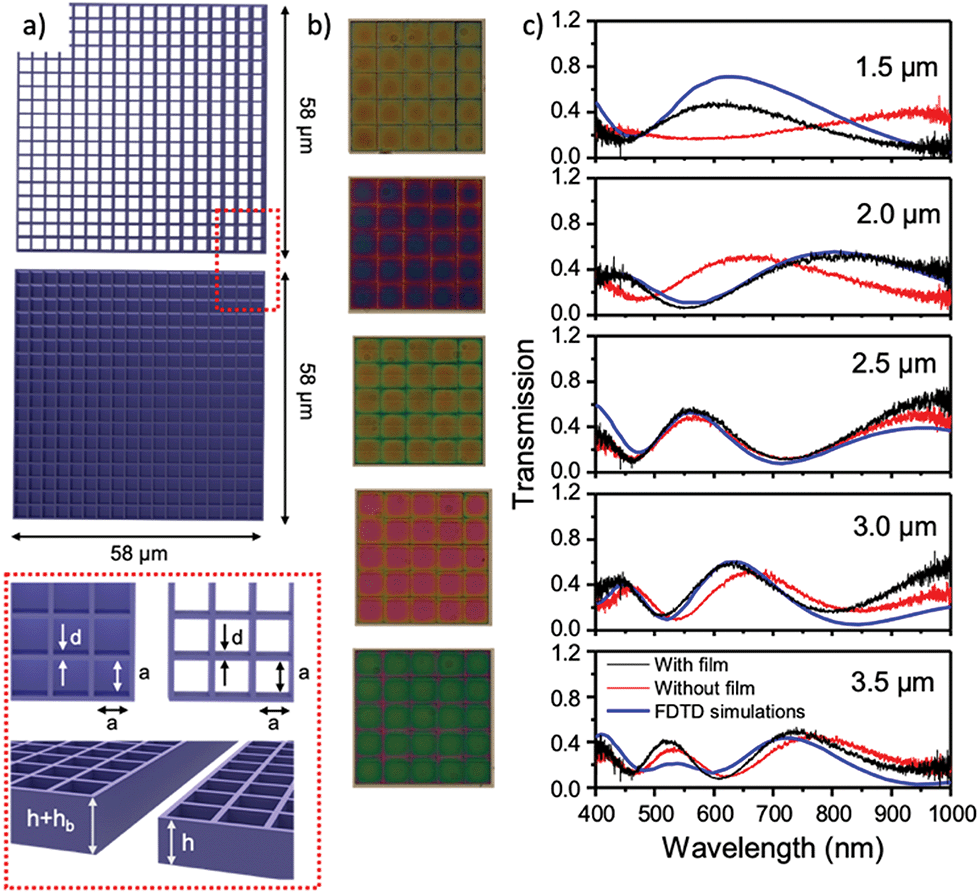 | ||
| Fig. 2 Design, images, and transmission spectra of photonic grid arrays. (a) The photonic structures were achieved through sequential fabrication of 58 μm × 58 μm repeating units of designed line width (d), height (h) and distance between parallel lines (a). For improved control of grid height during the DLW fabrication process, a second iteration contained a thin film underneath the photonic structures, of a nominal height (hb). (b) Transmission optical microscopy images of the fabricated structures with the film underneath, where the designed height of the grid structure is (top to bottom) 1.5 μm, 2.0 μm, 2.5 μm, 3.0 μm and 3.5 μm, respectively. (c) Corresponding measured transmission spectra with and without the under-structure film, and comparison with FDTD simulated spectra for grid structures of designed dimensions (a, d and h). | ||
In DLW, discrepancies in the design and fabricated grid heights can often be caused by minor variations in interface values between the substrate and monomeric photoresist (Fig. S4, S7 and S11–S13, ESI†). Inclusion of a thin film (hb = 1.0 μm, Fig. 2a) underneath the structures, serves to compensate for any variation in height (Fig. S1, ESI†), resulting in greater homogeneity across structures and better agreement with simulated spectra, as shown in Fig. 2c and Fig. S11 (ESI†). From the simulations, presented in greater detail in Fig. S4 (ESI†), it is clear that variation in square size (here represented by a, the distance between two neighbouring lines) has only a minimal impact on peak positions in the predicted spectrum. Variation of height (h) and line width (d), however, are seen to have a dramatic impact on the position of main spectral bands and the relative intensity number of resulting peaks and troughs.
As the material used for these microstructures is based on the hydrophilic acrylamide monomer, they have the ability to swell in the presence of polar solvents in the liquid and vapour state. To interrogate the possibility of employing this behaviour to yield a measurable visual response upon exposure to different vapours, we developed a simple bubbling system, in which gas vapours were transported using dry air as a carrier, through a flow-in flow-out quartz cell. By initially exposing the samples to a flow of compressed dry air, it was possible to eliminate any contributions from relative humidity changes in the environment. Capturing images and transmission spectra using a bespoke optical system (Fig. S2, ESI†), the optical response of the arrays was observed in real time. To study the spectral diversity of vapour responses of the photonic structures, three model solvents were selected, namely isopropanol, ethanol, and water. The dynamic responses of arrays upon exposure to these solvent vapours over the whole visible spectrum is exemplified in Fig. 3 for a 3.5 μm tall array. The observed red shift in the transmission spectrum increased with the polarity of solvent (isopropanol < ethanol < water) and was greater for higher flow rate of the exposing solvent (Fig. S15, ESI†). The redshift of the spectral peaks indicates increased size of the grid linewidth and height (Fig. S4 and S17, ESI†) and can be used to accurately differentiate the response from a mere influence of modulating ambient refractive index. It is also noteworthy that, while the presence of a thin base layer underneath the grids served to produce greater homogeneity of height and colour, the arrays fabricated without this layer exhibit larger spectral shifts (Fig. S16, ESI†). This can be attributed to a greater symmetry of expansion, upon introduction of the underlying film, by overcoming the restriction caused by direct attachment of the grid to the substrate.
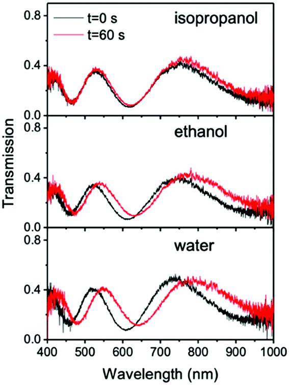 | ||
| Fig. 3 Transmission spectra of the photonic structures of designed height h = 3.5 μm with film, before (black) and after 1 min in the presence of solvent vapours (isopropanol – top; ethanol – middle and water – bottom) where the gas vapours were transported using dry air at a flow rate of 1 L min−1. | ||
The fast and notable response gave the opportunity to follow the spectral changes in real time. An example of such a response to water vapour is shown Fig. 4.
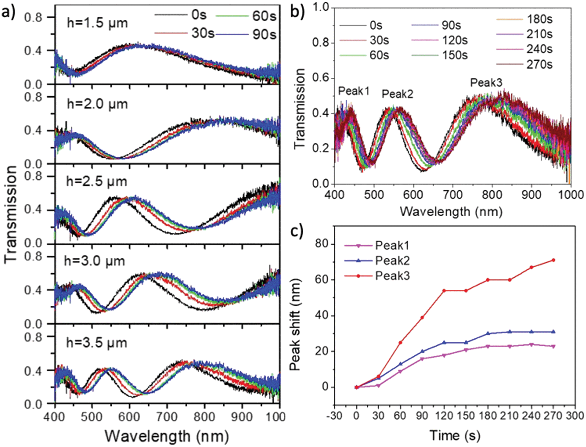 | ||
| Fig. 4 (a) Transmission spectra of the photonic structures of different designed heights (top to bottom: 1.5 μm, 2.0 μm, 2.5 μm, 3.0 μm and 3.5 μm) at different time points, under a 1 L min−1 flow of water vapour. (b) Transmission spectra of a nominated array of h = 3.5 μm in the presence of water vapours over time (0–270 s). (c) Data extracted from b showing the peak shift over time in the presence of water vapours (dry air carrier flow rate was 0.5 L min−1) for the three maxima. Integration time was set to 3.94 s. | ||
Fig. 4a shows a significant red shift in the spectral bands which is observed upon coming in contact with water vapour. The response increases with respective height of the arrays. The greatest shift in wavelength in all cases, combined with a significant peak broadening, is observed for the longest wavelength band in the transmission spectrum of each array (Fig. 4c). The transmission spectra, in the presence of the water vapour for a flow rate of 1 L min−1, can be simulated for a 5% to 7.5% expansion of the linewidth and height (Fig. S16, ESI†).
Fascinated by the dynamic response of different arrays, we sought to fabricate a rudimentary pixelated sensor, in which the different colours are achieved using different height arrays (Fig. 5). Five different heights, from 1.5 to 3.5 μm, were woven sequentially up and down, creating a reoccurring pattern of orange (1.5 μm), blue (2.0 μm), red (2.5 μm), pink (3.0 μm), and green (3.5 μm). In the presence of water vapour the colours are seen to rapidly change, shown in Fig. 5b, with the most dramatic response visible for the higher arrays. Upon accumulating large amounts of water, which serves to fully hydrate the structure and to condense in the voids, the visible photonic response of the thinner arrays is completely disrupted, revealing a pattern created only by the taller arrays (Fig. 5c). SEM images of this array, in Fig. S18 (ESI†), serve as a useful comparator. Within 4 seconds of ceasing the water vapour flow, the initial state fully returns (Fig. 5d). This can be used, quite impressively, to generate appearing and disappearing motifs whose colour and responsiveness can be pre-programmed into the fabricated design. The resulting spectral differences can be further explored to analyse the vapor-response diversity of the sensor, by employing principal components analysis (PCA) and hierarchical cluster analysis (HCA) tools. These approaches are extremely beneficial in deciphering the nature of diverse spectral features caused by exposures of the sensor to different vapours and vapour concentrations.
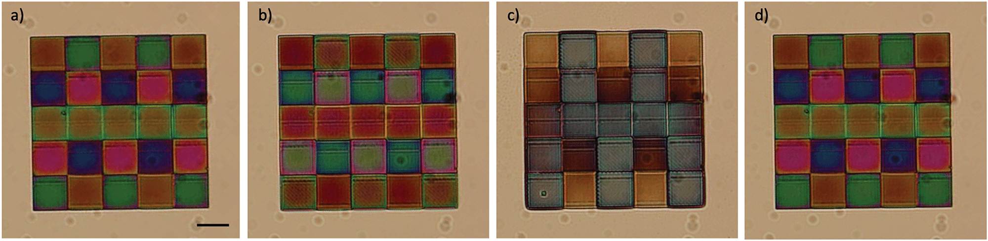 | ||
Fig. 5 (a) Transmission image of a grid array where each column is composed of five repeating units of different heights (left column, the designed height of the grid structure is (top to bottom) 1.5 μm, 2.0 μm, 2.5 μm, 3.0 μm and 3.5 μm, respectively). (b) The same array upon exposure to water vapours for approximately 20 s (Video S1, ESI.†t = 0![[thin space (1/6-em)]](https://www.rsc.org/images/entities/char_2009.gif) :26) and (c) upon saturation with water vapours for approximately 88 s (Video S1, ESI.†t = 1:34). (d) The array returns to its original colour 4 s after the gas flow is stopped. A flow rate of 1 L min−1 was used for the dry air carrier gas. Scale bar represents 50 μm. :26) and (c) upon saturation with water vapours for approximately 88 s (Video S1, ESI.†t = 1:34). (d) The array returns to its original colour 4 s after the gas flow is stopped. A flow rate of 1 L min−1 was used for the dry air carrier gas. Scale bar represents 50 μm. | ||
Additionally, more complex 3D structures can also be realised, showing that the material reported here is suitable for 2PP-fabrication of self-supporting 3-dimensional periodic structure. This is demonstrated through the fabrication of a woodpile structure, comprising 15 sequentially layered lines, which is presented in Fig. S9, ESI.†
Conclusions
A soft, hydrogel material was fabricated into a responsive photonic array with sub-micron features. This was made possible through the use of an appropriate ionic liquid co-solvent, which allowed for dissolution of all components and subsequent fabrication using DLW. The resulting periodic structures swell reversibly in the presence of solvent vapours, to generate a measurable optical response which is determined by the polarity of the solvent. The working principle is explained using FDTD analysis, where the experimental colour and wavelength changes are correlated with changes in the dimensions of the structures in real time. The principle presented herein can be applied to a wide range of polymer formulations (including stimuli-responsive hydrogels) and structural designs, to achieve functional photonic structures that will grant the desired spectral changes in response to the stimulus of interest.Conflicts of interest
There are no conflicts to declare.Acknowledgements
This research received funding from the European Research Council (ERC) Starting Grant (No. 802929 – ChemLife), Science Foundation Ireland (SFI), and European Regional Development Fund (ERDF) under grant number 12/RC/2278_P2. CD acknowledges support from the Irish Research Council through the Government of Ireland Postdoctoral Fellowship Scheme; Grant Number GOIPD/2020/484. LF also acknowledges funding from the European Horizon 2020 Research and Innovation Programme (No. 899349 – 5D NanoPrinting). JQ acknowledges funding from the Chinese Scholarship Council. ALB acknowledges SFI under Grant number 16/IA/4550. The TPP-DLW fabrication and the imaging for this project were carried out at the Additive Research Laboratory (AR-Lab) and the Advanced Microscopy Laboratory (AML), Trinity College Dublin, Ireland. The AR-Lab and AML are SFI supported centres, part of the CRANN Institute and affiliated to the AMBER centre.Notes and references
- C. Fenzl, T. Hirsch and O. S. Wolfbeis, Angew. Chem., Int. Ed., 2014, 53, 3318–3335 CrossRef CAS PubMed.
- R. A. Potyrailo, N. Karker, M. A. Carpenter and A. Minnick, J. Opt., 2018, 20, 024006 CrossRef.
- S. Daqiqeh Rezaei, Z. Dong, J. You En Chan, J. Trisno, R. J. H. Ng, Q. Ruan, C.-W. Qiu, N. A. Mortensen and J. K. W. Yang, ACS Photonics, 2021, 8, 18–33 CrossRef CAS.
- R. A. Potyrailo, R. K. Bonam, J. G. Hartley, T. A. Starkey, P. Vukusic, M. Vasudev, T. Bunning, R. R. Naik, Z. Tang, M. A. Palacios, M. Larsen, L. A. Le Tarte, J. C. Grande, S. Zhong and T. Deng, Nat. Commun., 2015, 6, 7959 CrossRef PubMed.
- S. Daqiqeh Rezaei, J. Ho, T. Wang, S. Ramakrishna and J. K. W. Yang, Nano Lett., 2020, 20, 4422–4429 CrossRef CAS PubMed.
- E. D. Le Boulbar, C. J. Lewins, D. W. E. Allsopp, C. R. Bowen and P. A. Shields, Microelectron. Eng., 2016, 153, 132–136 CrossRef CAS.
- C. Delaney, N. Geoghegan, H. Ibrahim, M. O’Loughlin, B. Rodriguez, L. Florea and S. Kelleher, ACS Appl. Polym. Mater., 2020, 2, 3632–3641 CrossRef CAS.
- M. Pozo, C. Delaney, C. Bastiaansen, D. Diamond, A. Schenning and L. Florea, ACS Nano, 2020, 14, 9832–9839 CrossRef PubMed.
- R. M. Almeida, L. M. Fortes and M. Clara Gonçalves, Opt. Mater., 2011, 33, 1867–1871 CrossRef CAS.
- A. J. J. Kragt, R. C. G. M. Loonen, D. J. Broer, M. G. Debije and A. P. H. J. Schenning, J. Polym. Sci., 2021, 59, 1278–1284 CrossRef CAS.
- A. A. F. Froyen, M. Wübbenhorst, D. Liu and A. P. H. J. Schenning, Adv. Electron. Mater., 2021, 7, 2000958 CrossRef CAS.
- A. Belmonte, M. Pilz da Cunha, K. Nickmans and A. P. H. J. Schenning, Adv. Opt. Mater., 2020, 8, 2000054 CrossRef CAS.
- L. Zheng, K. Kurselis, A. El-Tamer, U. Hinze, C. Reinhardt, L. Overmeyer and B. Chichkov, Nanoscale Res. Lett., 2019, 14, 134 CrossRef PubMed.
- M. Malinauskas, A. Gaidukevičiūtė, V. Purlys, A. Žukauskas, I. Sakellari, E. Kabouraki, A. Candiani, D. Gray, S. Pissadakis, R. Gadonas, A. Piskarskas, C. Fotakis, M. Vamvakaki and M. Farsari, Metamaterials, 2011, 5, 135–140 CrossRef CAS.
- G. Zyla, A. Kovalev, M. Grafen, E. L. Gurevich, C. Esen, A. Ostendorf and S. Gorb, Sci. Rep., 2017, 7, 1–9 CrossRef CAS PubMed.
- G. Zyla, A. Kovalev, E. L. Gurevich, C. Esen, Y. Liu, Y. Lu, S. Gorb and A. Ostendorf, Appl. Phys. A: Mater. Sci. Process., 2020, 126, 740 CrossRef CAS.
- G. Zyla, A. Kovalev, S. Heisterkamp, C. Esen, E. L. Gurevich, S. Gorb and A. Ostendorf, Opt. Mater. Express, 2019, 9, 2630–2639 CrossRef CAS.
- Y. Liu, H. Wang, J. Ho, R. C. Ng, R. J. H. Ng, V. H. Hall-Chen, E. H. H. Koay, Z. Dong, H. Liu, C.-W. Qiu, J. R. Greer and J. K. W. Yang, Nat. Commun., 2019, 10, 4340 CrossRef PubMed.
- W. Zhang, H. Wang, H. Wang, J. Y. E. Chan, H. Liu, B. Zhang, Y.-F. Zhang, K. Agarwal, X. Yang, A. S. Ranganath, H. Y. Low, Q. Ge and J. K. W. Yang, Nat. Commun., 2021, 12, 112 CrossRef CAS PubMed.
- M. Carlotti and V. Mattoli, Small, 2019, 15, 1902687 CrossRef PubMed.
- A. K. Nguyen and R. J. Narayan, Mater. Today, 2017, 20, 314–322 CrossRef CAS.
- D. Gräfe, S. L. Walden, J. Blinco, M. Wegener, E. Blasco and C. Barner-Kowollik, Angew. Chem., Int. Ed., 2020, 59, 6330–6340 CrossRef PubMed.
- A. Tudor, C. Delaney, H. Zhang, A. J. Thompson, V. F. Curto, G.-Z. Yang, M. J. Higgins, D. Diamond and L. Florea, Mater. Today, 2018, 21, 807–816 CrossRef CAS.
- N. Buch-Månson, A. Spangenberg, L. P. C. Gomez, J. P. Malval, O. Soppera and K. L. Martinez, Sci. Rep., 2017, 7, 1–9 CrossRef PubMed.
- A. Marino, G. Ciofani, C. Filippeschi, M. Pellegrino, M. Pellegrini, P. Orsini, M. Pasqualetti, V. Mattoli and B. Mazzolai, ACS Appl. Mater. Interfaces, 2013, 5, 13012–13021 CrossRef CAS PubMed.
- D. H. Kim, P. Kim, K. Y. Suh, S. K. Choi, S. H. Lee and B. Kim, Annu. Int. Conf. IEEE Eng. Med. Biol. - Proc., 2005, vol. 7, 4091–4094.
- M. Hippler, E. Blasco, J. Qu, M. Tanaka, C. Barner-Kowollik, M. Wegener and M. Bastmeyer, Nat. Commun., 2019, 10, 232 CrossRef PubMed.
- D. Jin, Q. Chen, T.-Y. Huang, J. Huang, L. Zhang and H. Duan, Mater. Today, 2020, 32, 19–25 CrossRef CAS.
- Y.-L. Zhang, Y. Tian, H. Wang, Z.-C. Ma, D.-D. Han, L.-G. Niu, Q.-D. Chen and H.-B. Sun, ACS Nano, 2019, 13, 4041–4048 CrossRef CAS PubMed.
- L. C. Tomé and D. Mecerreyes, J. Phys. Chem. B, 2020, 124, 8465–8478 CrossRef PubMed.
Footnotes |
| † Electronic supplementary information (ESI) available. See DOI: 10.1039/d1tc01796a |
| ‡ These authors contributed equally. |
| This journal is © The Royal Society of Chemistry 2021 |