
Impact of grain size on the optoelectronic performance of 2D Ruddlesden–Popper perovskite-based photodetectors†
Bohee
Hwang‡
,
Youngjun
Park‡
and
Jang-Sik
Lee
 *
*
Materials Science and Engineering, Pohang University of Science and Technology (POSTECH), Pohang 37673, Korea. E-mail: jangsik@postech.ac.kr; Tel: +82 54-279-2153
First published on 23rd November 2020
Abstract
Two-dimensional (2D) Ruddlesden–Popper perovskites have been spotlighted as photodetectors due to their tunable bandgap and high photoluminescence quantum efficiency. The performance of photodetectors is affected by grain boundaries that can trap charge carriers and thereby degrade charge transport in perovskites. To fabricate high-performance photodetectors, it is important to control the grain boundaries of the perovskite film. Here, we use a hot casting method to synthesize highly-crystalline, large-grained films of 2D Ruddlesden–Popper perovskites (C4H9NH3)2(CH3NH3)Pb2I7 for use in improving the efficiency of photodetectors. Increasing the grain size of the perovskite film alleviates the effects of grain boundaries. To control the grain size of the film, the composition of the precursor mixture N,N-dimethylformamide (DMF) and dimethyl sulfoxide (DMSO) is varied. As the DMSO content increases, the grain size of the film increases from the nanometer to the micrometer scale. Photodetectors fabricated using films with large grains show high photocurrent and on/off ratio compared to those with small grains. This method to synthesize 2D Ruddlesden–Popper perovskite films with tailored grain sizes can facilitate the fabrication of highly-efficient optoelectronic devices.
Introduction
Organic–inorganic hybrid perovskites (OIPs) including three-dimensional (3D) or layered two-dimensional (2D) structures have excellent charge carrier transport, a long electron–hole diffusion length, and a tunable bandgap, due to which they have applications in optoelectronics.1–7 Development to implement the superior optoelectronic properties of OIPs has led to the design of various applications such as solar cells, photodetectors,8,9 lasers,10,11 and photo supercapacitors.12,13 Besides, to improve the optical properties of OIPs, several methods including the doping of small molecules in OIPs, the use of OIP quantum dots, and the introduction of multilayer structures have been proposed.14–16 In addition, by lowering the dimensions from 3D to 2D, 2D Ruddlesden–Popper layered perovskite (RPLP) materials have attracted considerable attention for OIP-based optoelectronic applications.17–21 2D RPLP materials have weak ionic bonding, so they can be grown easily using vapor transport or solution processes.22 Moreover, functionalization with appropriate functional organic groups during synthesis yields RPLP films that have tunable structures and properties; improved optoelectronic properties and environmental stability compared to those of 3D OIPs.23–27To improve the optical properties such as photocurrent and power conversion efficiency (PCE) of an OIP-based optoelectronic devices, the grain size of the film should be optimized.28,29 Increasing the grain size in OIP-based polycrystalline films alleviates the effects of grain boundaries that can trap the charge carriers and thereby degrade the charge transport in OIPs.30 In 2D RPLP films, which consist of an inorganic layer sandwiched between organic spacers, the influence of grain size and crystal orientation is important because they affect the anisotropic charge transport in the films.31 Charge transport between grains in 2D RPLP films can be enhanced by increasing the grain size and thereby reducing the number of grain boundaries. Therefore, various methods have been investigated to increase the grain size in OIP-based films such as hot-casting,32,33 solvent engineering,34 and thermal nanoimprint technology.35,36 Among them, crystal growth depends on the substrate temperature; so, the hot-casting method allows the grain size to reach the millimeter scale.32 Furthermore, the grain size can be controlled by choosing an appropriate solvent. In (CH3(CH2)2NH3)2(CH3NH3)4Pb5I16 films, an optimized mixture of N,N-dimethylformamide (DMF) and dimethyl sulfoxide (DMSO) could increase the grain size from nanoscale to microscale, which resulted in solar cells having a high PCE.37 Although several studies on controlling the grain size have been conducted in solar cells, it is also essential to investigate the effect of grain size on photodetectors to improve the device performance.
In this study, we synthesize (C4H9NH3)2(CH3NH3)Pb2I7 (BA2MAPb2I7, where BA = butylammonium; MA = methylammonium) films using a hot-casting method and solvent engineering to achieve a highly sensitive photodetector. We quantify the effect of grain sizes on the optical response of the photodetector using polar solvents DMSO and DMF, either pure or mixed. The improvement in optoelectronic performance can be obtained by increasing the grain size of the film with a reduced number of grain boundaries. This method to synthesize BA2MAPb2I7 films can suggest a way to control the grain size and improve the device performance in optoelectronic applications.
Experimental section
Materials
Butylammonium iodide (BAI) and methylammonium iodide (MAI) were purchased from Greatcell Solar. Lead bromide (PbI2, 99% purity), N,N-dimethylformamide (DMF, ≥99.8% purity), and dimethyl sulfoxide (DMSO, ≥99.9% purity) were purchased from Sigma-Aldrich. Si wafers with 100 nm thick thermally-grown SiO2 were used as the substrate. All materials were used without further purification.Device fabrication
Before device fabrication, the SiO2/Si substrate was cleaned sequentially with ethanol, acetone, and deionized water. The BA2MAPb2I7 precursor solution was composed of PbI2, BAI, and MAI (2![[thin space (1/6-em)]](https://www.rsc.org/images/entities/char_2009.gif) :2:1) in solvents (DMF and DMSO) in different volume ratios [PDMSO = DMSO/(DMSO + DMF)] of 1:0 (PDMSO = 0), 7:3 (PDMSO = 0.3), 1:1 (PDMSO = 0.5), 3:7 (PDMSO = 0.7) and 0:1 (PDMSO = 1). During hot-casting, the substrate was heated to 200 °C and the precursor solution was kept on a hot plate at 70 °C.32 During spin coating, the hot substrate was transferred to the spin coater chuck; the transfer time was about 1–2 s. The precursor solution was then spun at 1250 rpm for 60 s in a nitrogen atmosphere. The resulting films were allowed to cool down to room temperature, and then planar photodetectors were fabricated by thermally evaporating 50 nm thick Au electrodes through a shadow mask. The size of Au electrodes was 0.1 mm2 and the distance between electrodes was 100 μm.
:2:1) in solvents (DMF and DMSO) in different volume ratios [PDMSO = DMSO/(DMSO + DMF)] of 1:0 (PDMSO = 0), 7:3 (PDMSO = 0.3), 1:1 (PDMSO = 0.5), 3:7 (PDMSO = 0.7) and 0:1 (PDMSO = 1). During hot-casting, the substrate was heated to 200 °C and the precursor solution was kept on a hot plate at 70 °C.32 During spin coating, the hot substrate was transferred to the spin coater chuck; the transfer time was about 1–2 s. The precursor solution was then spun at 1250 rpm for 60 s in a nitrogen atmosphere. The resulting films were allowed to cool down to room temperature, and then planar photodetectors were fabricated by thermally evaporating 50 nm thick Au electrodes through a shadow mask. The size of Au electrodes was 0.1 mm2 and the distance between electrodes was 100 μm.
Measurement and characterization
The crystal structure was measured using an X-ray diffractometer (XRD; Rigaku D/MAX-2500) with Cu Kα radiation at a step size of 0.02°. The morphological images of the surface and cross-section were captured using a high-resolution field-emission scanning-electron microscope (SEM; JEOL JSM-7800F Prime) with a 10 kV acceleration voltage and an atomic-force microscope (AFM; VEECO Dimension 3100). Photoluminescence (PL) spectra were measured using a spectrometer (Horiba LabRAM HR-800). Time-resolved photoluminescence (TRPL) was measured using a time-correlated single-photon counting system (HAMAMATSU C11367-31). Current–voltage (I–V) characteristics were measured using a semiconductor parameter analyzer (Keithley 4200A-SCS) in a vacuum probe station. The optical response measurements were made by applying monochromatic light from a xenon lamp (Newport 71SI00059) under ambient conditions. Grain sizes G were calculated using the ASTM E112 intercept method.32G was calculated as G = 6.643856log10(PL) −3.288, where PL is the number of grain boundary intersections per unit length of the test line and was determined using PL = Pi/(L/M), where Pi is the total number of intercepts of all test lines, L is the total length of test lines, and M is the magnification.
Results and discussion
A 2D RPLP with the chemical formula (RNH3)2(CH3NH3)n−1MX3n+1, where RNH3 is a long chain organic cation, M is a metal cation, and X is a halide anion, was selected to evaluate the morphology, texture, and performance of the photodetector. To increase the grain size and improve the crystallinity of the 2D RPLP films, we combined solvent engineering with the hot casting method (Fig. 1a).32 The morphology and grain size of BA2MAPb2I7 films can be influenced by crystallization kinetics such as the rate of solvent evaporation. LaMer's graph is used to explain the nucleation and growth processes, which are related to the concentration change of the solution over time (Fig. 1b).38 As the solvent evaporates, the solution concentration reaches the saturation concentration Cs; then, when the solution concentration exceeds the critical value Cc, nuclei start to form and then grow by consuming the solute. Slow evaporation of the solvent leads to rapid growth of the nuclei due to fast consumption of the solute. This hypothesis suggests that the increase in the grain size of BA2MAPb2I7 films after the addition of DMSO to DMF occurs because the mixture evaporates more slowly than pure DMF. The crystallization process of BA2MAPb2I7 films was suggested using pure DMF solution and the mixture of DMF/DMSO solution by considering LaMer's graph (Fig. 1c). The vapor pressure of the solvent influences its evaporation rate, and this change can affect the morphology and grain size of the film. As reported previously, DMF has a higher vapor pressure than DMSO,39 so DMF evaporates quickly during the spin coating process. When the precursor concentration exceeds Cc, the BA2MAPb2I7 film obtained using DMF solution nucleates and grows quickly because of the fast evaporation of DMF.40 However, DMSO has a lower vapor pressure (0.42 mmHg) than DMF (2.7 mmHg).41 Adding DMSO to DMF impedes the evaporation of the solvent during the spin-coating process, so the solvent evaporates slowly and thereby extends the time required for the precursor concentration to reach Cc. Also, considering the large grain size of the film that was obtained using PDMSO = 0.7, the nucleation period (t1′–t2′) of the film that was synthesized from the DMF and DMSO mixture may be longer than the nucleation period (t1–t2) of the film that was obtained from pure DMF. The XRD patterns of films that had been synthesized from different PDMSO showed (0k0) diffraction peaks (Fig. S1, ESI†). As the ratio of the DMSO increased, the intensity of (020) increased. These observations indicate that the addition of DMSO improved the crystal quality of the film. The improvement of crystallinity is thought to be related to the perovskite crystallization process. DMSO has a higher boiling point (189 °C) and a lower vapor pressure than DMF that has a lower boiling point of 152 °C and a higher vapor pressure.41 These characteristics induce the differences in the evaporation rates of solvents that can affect the crystallization rate and film quality during the spin-coating process.39 Due to these differences between DMSO and DMF, the crystallization kinetics are slower in the OIP film obtained using DMSO than those in the film obtained using DMF.37 As a result, the film formed using DMSO has better crystallinity than the film formed using DMF.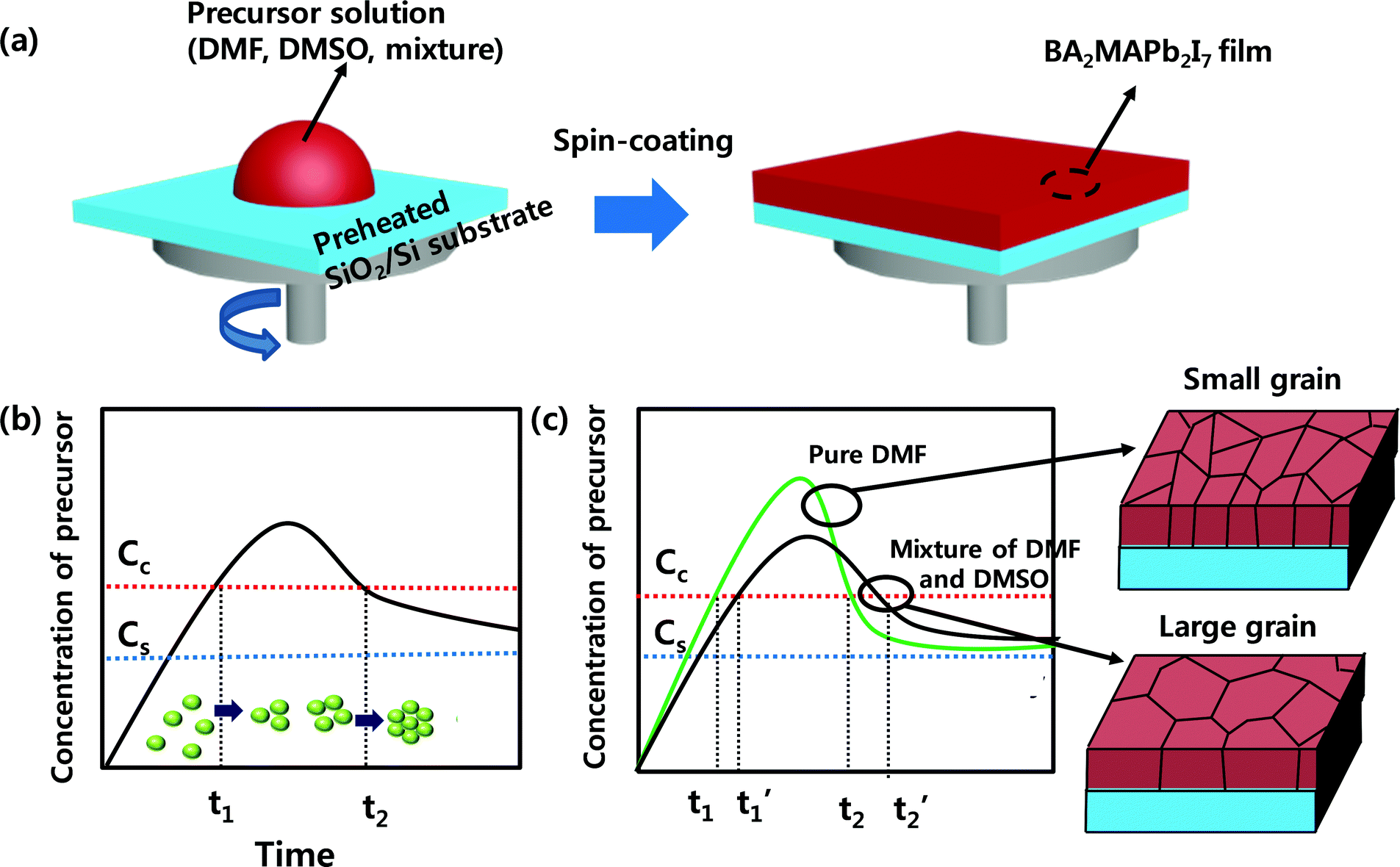 | ||
| Fig. 1 (a) Schematic illustration of the BA2MAPb2I7 thin film deposition process using hot-casting and solvent engineering. (b) LaMer's diagram and (c) modified LaMer's diagram for BA2MAPb2I7 film formation using pure DMF (PDMSO = 0) and a mixture of DMF and DMSO. Cs and Cc are the saturation concentration and critical concentration for nucleation, respectively. | ||
This phenomenon also affected the film morphology. Top-view SEM images of the films obtained using PDMSO = 0, 0.3, 0.5, 0.7, and 1 were taken (Fig. 2); as PDMSO increased, the grain size of the resulting BA2MAPb2I7 film increased (Fig. 2a–e), from the nanometer scale at PDMSO = 0 to the micrometer scale at PDMSO = 1. We also calculated the grain size of the film utilizing the ASTM intercept method.32 This method has been explained in the experimental section in detail. The average grain size of the film increased as PDMSO increased, i.e., from 0.6 ± 0.2 μm at PDMSO = 0 to 1.7 ± 0.7 μm at PDMSO = 0.3, 4.4 ± 0.5 μm at PDMSO = 0.5, 7.5 ± 1.2 μm at PDMSO = 0.7, and 14.1 ± 1.9 μm at PDMSO = 1 (Fig. 2f). Also, the BA2MAPb2I7 film obtained using PDMSO = 1 was uniformly formed with a thickness of about 350 nm (Fig. S2, ESI†). In addition, we used AFM to assess the quality of the BA2MAPb2I7 film. AFM (scan size = 10 μm × 10 μm) images showed that the film obtained using DMF (PDMSO = 0) had an average root-mean-squared roughness of Rrms = 24.5 nm, whereas the film obtained using DMSO (PDMSO = 1) had Rrms = 17.8 nm (Fig. S3, ESI†).
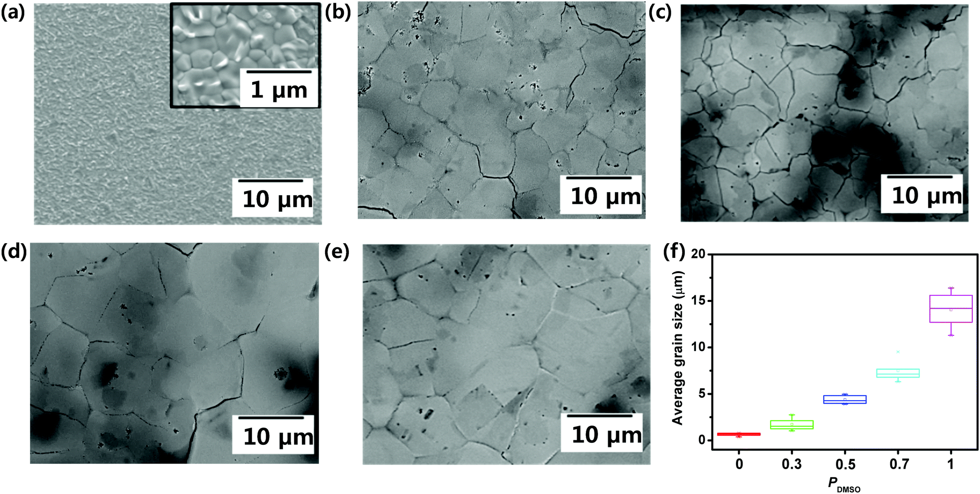 | ||
| Fig. 2 Plan-view SEM images of films cast from (a) pure DMF (PDMSO = 0) (inset: magnified image), (b) DMF:DMSO = 7:3 (PDMSO = 0.3), (c) DMF:DMSO = 1:1 (PDMSO = 0.5), (d) DMF:DMSO = 3:7 (PDMSO = 0.7), and (e) pure DMSO (PDMSO = 1). (f) Average grain sizes of BA2MAPb2I7 films cast from PDMSO = 0, 0.3, 0.5, 0.7, and 1. | ||
To measure the photosensitivity of the film obtained using BA2MAPb2I7, lateral photodetectors were fabricated by combining solvent engineering and hot-casting, with PDMSO = 0, 0.3, 0.5, 0.7, or 1. The schematic illustration and optical image of the fabricated photodetector device are shown in Fig. S4 (ESI†). Irradiation using the visible light produced electron–hole pairs in the OIP. In all devices, the current increased as the voltage increased (Fig. 3a). The I–V curves of BA2MAPb2I7-based photodetectors that were fabricated using PDMSO = 0, 0.3, 0.5, 0.7, or 1 were measured in the dark and under the illumination with a wavelength of 460 nm and an intensity (LI) of 300 μW cm−2 (Fig. 3b). In the dark, the photocurrent of the devices was ∼1 × 10⁻¹¹ A at a voltage bias of 30 V (Fig. S5, ESI†). The relationship between the photocurrent and incident light intensity of the films was shown (Fig. 3c). As the incident light intensity increased, the photocurrent increased; this trend confirms the light-sensitive properties of BA2MAPb2I7 films. The photocurrent of the devices was measured at a voltage bias of 30 V with a wavelength of 460 nm at different LI. As PDMSO increased, the photocurrent in the devices increased. The increase in photocurrent may have occurred because the films produced at PDMSO = 0.7 or 1 had larger grains, and therefore fewer grain boundaries, than the film produced at PDMSO = 0.
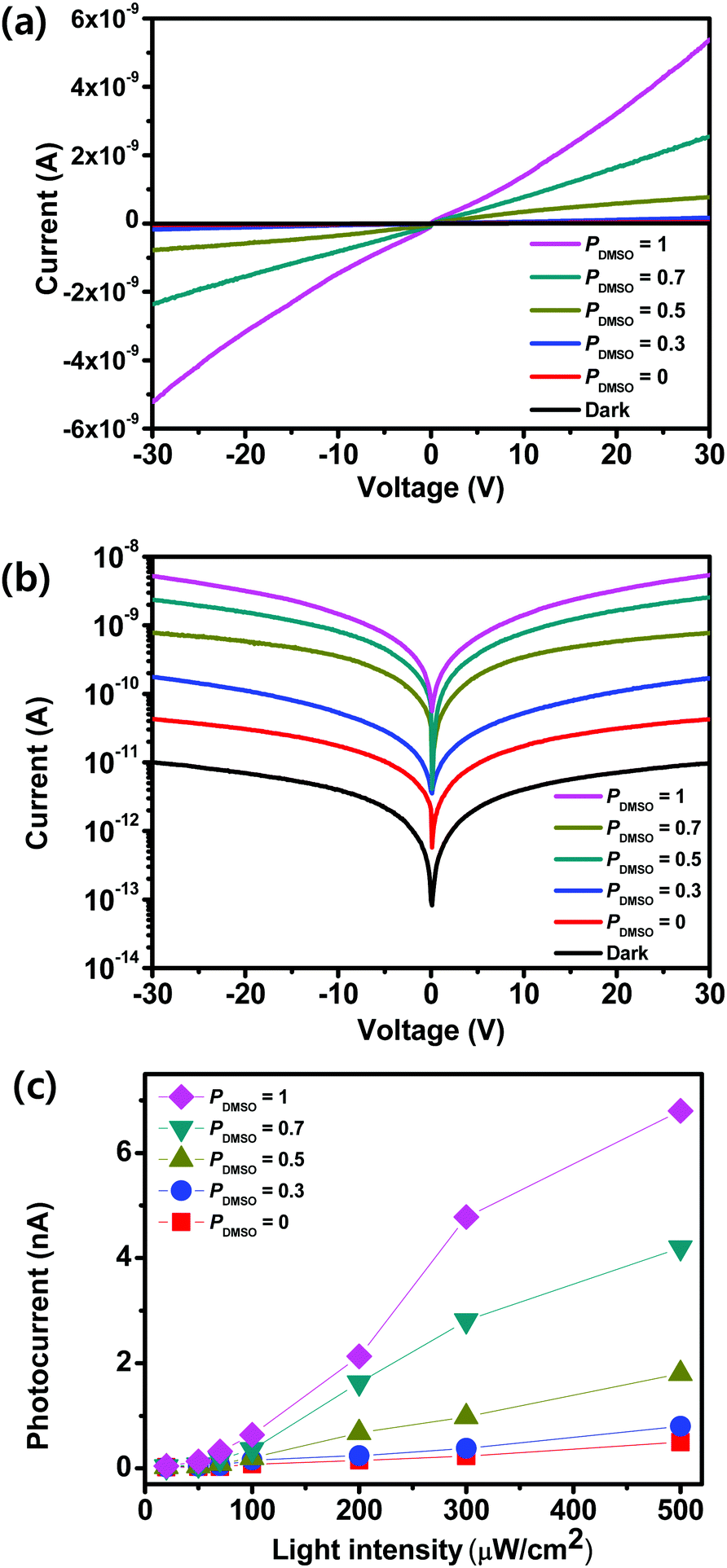 | ||
| Fig. 3 I–V characteristics of the photodetectors based on PDMSO = 0, 0.3, 0.5, 0.7, and 1 under irradiation with a light intensity of 300 μW cm−2 at a wavelength of 460 nm in the dark with (a) a linear scale and (b) a semilogarithmic scale. (c) Photoresponse of the film under 460 nm light with light intensities ranging from 20 μW cm−2 to 500 μW cm−2. | ||
We quantified the effect of LI on the photoresponse of the device obtained using PDMSO = 1 (Fig. 4a). The I–V characteristics were measured in the dark and under the illumination with a wavelength of 460 nm at 0 ≤ LI ≤ 300 μW cm−2 and a voltage bias of 30 V. As LI increased, the photocurrent increased from 1 × 10⁻¹¹ A in the dark to 5 × 10⁻⁹ A at 300 μW cm−2. An increase in LI induced increased generation of charge carriers, which yielded an increased photocurrent. The photoswitching properties of the devices were measured at a voltage bias of 30 V with 460 nm light illumination with a fixed LI = 300 μW cm−2 (Fig. 4b). The photocurrent increased sharply when the light was turned on and decreased sharply when it was turned off. The on/off current ratio was ∼120. Ten cycles of photoswitching were demonstrated that the device had reliable and stable photoresponses. To confirm the feasibility of the low-voltage operation of the fabricated photodetector, we measured the photoswitching properties of a device that had PDMSO = 1 at 5 V using 460 nm light illumination. The photocurrent increased sharply when the light was turned on and decreased when it was turned off (Fig. S6, ESI†). It showed that the photodetector devices could be operated at a low voltage. R is an important parameter to characterize sensitivity. We calculated R = (Ilight − Idark)/(LIA), where Ilight is the current under illumination, Idark is the current in the dark, and A is the active area in the device. The active area of the light illumination was 9 × 10⁻⁴ cm2. At a bias voltage of 30 V, as LI increased from 20 μW cm−2 to 500 μW cm−2, R decreased from 26.3 A W−1 to 1.4 A W−1 (Fig. 4c). We also quantified the effect of LI on the external quantum efficiency EQE = Rhc/(λe), where R is the responsivity of the photodetector, h is Planck constant, c is the speed of light, λ is the wavelength of incident light, and e is the electron charge.42,43 The calculated EQE was 2.2 × 10³% at 200 μW cm−2 (Fig. S7, ESI†). We then calculated D* = RA0.5/(2eIdark)0.5. D* decreased as LI increased (Fig. 4d), and the highest value was estimated to be 4 × 10¹² Jones (1 Jones = 1 cm Hz0.5 W−1). The photoresponse of the photodetector can be further improved by reducing the numbers of pinholes and defects, which can act as non-radiative recombination centers in OIP films.
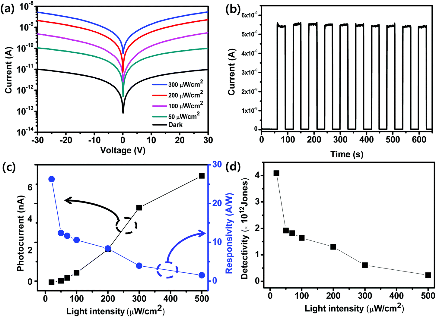 | ||
| Fig. 4 (a) I–V characteristics of the device that was fabricated using PDMSO = 1 in the dark and at different light intensities under 460 nm light illumination ranging from 50 μW cm−2 to 300 μW cm−2. (b) Photoswitching at a light intensity of 300 μW cm−2. (c) Photocurrent and responsivity as a function of light intensity. (d) Detectivity as a function of light intensity. | ||
We compared the absorption spectra and PL of the BA2MAPb2I7 films obtained using different PDMSO (Fig. 5). The BA2MAPb2I7 films that were synthesized with different PDMSO showed band edges at ∼602 nm (Fig. 5a); the corresponding optical bandgap was 2.05 eV, which is consistent with previous reports.9,44 The morphological change and the different grain sizes induced different optoelectronic properties such as PL. The films formed using PDMSO = 0.7 or 1 showed good crystallinity with large grain sizes and therefore had a higher PL intensity than that of the films formed using PDMSO = 0, 0.3, or 0.5 (Fig. 5b). The TRPL of BA2MAPb2I7 films with different PDMSO was measured to confirm the carrier lifetime of the films on the substrate, which could provide evidence that the quality of the film was improved by using DMSO (Fig. 5c). The PL decay of the films was fitted using a bi-exponential decay model.45,46 The fast decay component τ1 is related to charge carrier trapping, and the slow decay component τ2 indicates radiative recombination of free carriers.47,48 The film formed at PDMSO = 1 showed a higher PL lifetime (τ1 = 467 ns and τ2 = 1278 ns) than the film formed at PDMSO = 0 (τ1 = 360 ns and τ2 = 978 ns). The large grain size of the film with a reduced trap density may increase the PL lifetime.
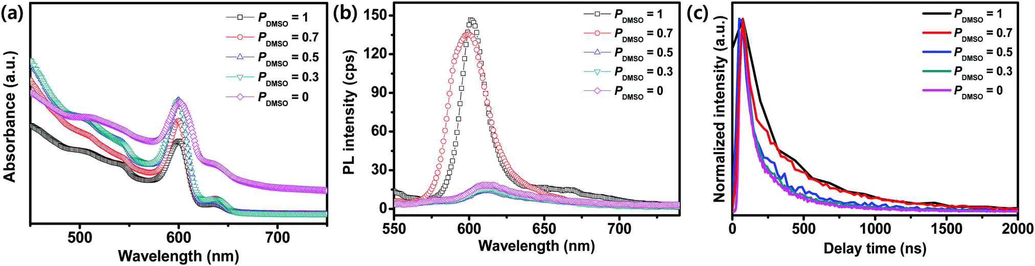 | ||
| Fig. 5 (a) Absorbance, (b) photoluminescence (PL), and (c) time-resolved PL (TRPL) spectra of the films cast from PDMSO = 0, 0.3, 0.5, 0.7, and 1. | ||
Conclusions
We demonstrated the control of grain size in BA2MAPb2I7 films by combining solvent engineering and the hot casting method. Introducing DMSO into DMF increased the grain size of BA2MAPb2I7 films and improved the quality of the film. As the grain size of the film increased, the photocurrent and on/off ratio increased. The photodetector that was fabricated using pure DMSO exhibited the largest grain size and the highest photocurrent, R, and D*. The improved device performance using the film that had a large grain size could be explained by a decrease in the number of carrier recombination sites, because of a reduced number of grain boundaries and a decrease of defect density. The proposed method to control the grain size of films may enable the development of high-quality perovskite films that can be applied to advanced optoelectronics.Author contributions
J.-S. L. conceived and directed the research. J.-S. L. and B. H. designed and planned the experiments. B. H. and Y. P. performed the experiments and acquired the data. B. H., Y. P., and J.-S. L. wrote the manuscript.Conflicts of interest
There are no conflicts to declare.Acknowledgements
This work was supported by the National Research Foundation of Korea (NRF-2016M3D1A1027665 and NRF-2019R1A2C2084114). This work was also supported by the Industrial Strategic Technology Development Program (20003968) funded by the Ministry of Trade, Industry & Energy (MOTIE, Korea). In addition, this work was partially supported by the Brain Korea 21 PLUS project (Center for Creative Industrial Materials).References
- H. J. Snaith, Nat. Mater., 2018, 17, 372–376 CrossRef CAS.
- R. Quintero-Bermudez, A. Gold-Parker, A. H. Proppe, R. Munir, Z. Yang, S. O. Kelley, A. Amassian, M. F. Toney and E. H. Sargent, Nat. Mater., 2018, 17, 900–907 CrossRef CAS.
- Y. P. Fu, H. M. Zhu, J. Chen, M. P. Hautzinger, X. Y. Zhu and S. Jin, Nat. Rev. Mater., 2019, 4, 169–188 CrossRef CAS.
- W. D. Xu, Q. Hu, S. Bai, C. X. Bao, Y. F. Miao, Z. C. Yuan, T. Borzda, A. J. Barker, E. Tyukalova, Z. J. Hu, M. Kawecki, H. Y. Wang, Z. B. Yan, X. J. Liu, X. B. Shi, K. Uvdal, M. Fahlman, W. J. Zhang, M. Duchamp, J. M. Liu, A. Petrozza, J. P. Wang, L. M. Liu, W. Huang and F. Gao, Nat. Photonics, 2019, 13, 418–424 CrossRef CAS.
- Y. H. Deng, X. P. Zheng, Y. Bai, Q. Wang, J. J. Zhao and J. S. Huang, Nat. Energy, 2018, 3, 560–566 CrossRef CAS.
- S. I. Seok, M. Gratzel and N. G. Park, Small, 2018, 14, 1704177 CrossRef.
- Q. Van, H. W. Le Jang and S. Y. Kim, Small Methods, 2018, 2, 1700419 CrossRef.
- C. Bao, J. Yang, S. Bai, W. Xu, Z. Yan, Q. Xu, J. Liu, W. Zhang and F. Gao, Adv. Mater., 2018, 30, 1803422 CrossRef.
- B. Hwang and J.-S. Lee, Adv. Opt. Mater., 2019, 7, 1801356 CrossRef.
- C. M. Raghavan, T. P. Chen, S. S. Li, W. L. Chen, C. Y. Lo, Y. M. Liao, G. Haider, C. C. Lin, C. C. Chen, R. Sankar, Y. M. Chang, F. C. Chou and C. W. Chen, Nano Lett., 2018, 18, 3221–3228 CrossRef CAS.
- Q. Wei, X. J. Li, C. Liang, Z. P. Zhang, J. Guo, G. Hong, G. C. Xing and W. Huang, Adv. Opt. Mater., 2019, 7, 1900080 CrossRef.
- J. Liang, G. Y. Zhu, C. X. Wang, P. Y. Zhao, Y. R. Wang, Y. Hu, L. B. Ma, Z. X. Tie, J. Liu and Z. Jin, Nano Energy, 2018, 52, 239–245 CrossRef CAS.
- J. Liang, G. Y. Zhu, Z. P. Lu, P. Y. Zhao, C. X. Wang, Y. Ma, Z. R. Xu, Y. R. Wang, Y. Hu, L. B. Ma, T. Chen, Z. X. Tie, J. Liu and Z. Jin, J. Mater. Chem. A, 2018, 6, 2047–2052 RSC.
- A. A. Khan, Z. Yu, U. Khan and L. Dong, Nanoscale Res. Lett., 2018, 13, 399 CrossRef.
- Y. Z. Wei, Z. W. Ren, A. D. Zhang, P. Mao, H. Li, X. H. Zhong, W. W. Li, S. Y. Yang and J. Z. Wang, Adv. Funct. Mater., 2018, 28, 1706690 CrossRef.
- A. A. Khan, M. Azam, D. Eric, G. X. Liang and Z. N. Yu, J. Mater. Chem. C, 2020, 8, 2880–2887 RSC.
- S. Yuan, Z. K. Wang, L. X. Xiao, C. F. Zhang, S. Y. Yang, B. B. Chen, H. T. Ge, Q. S. Tian, Y. Jin and L. S. Liao, Adv. Mater., 2019, 31, 1904319 CrossRef CAS.
- C. M. M. Soe, W. Nie, C. C. Stoumpos, H. Tsai, J.-C. Blancon, F. Liu, J. Even, T. J. Marks, A. D. Mohite and M. G. Kanatzidis, Adv. Energy Mater., 2018, 8, 1700979 CrossRef.
- H. Tsai, W. Nie, J. C. Blancon, C. C. Stoumpos, R. Asadpour, B. Harutyunyan, A. J. Neukirch, R. Verduzco, J. J. Crochet, S. Tretiak, L. Pedesseau, J. Even, M. A. Alam, G. Gupta, J. Lou, P. M. Ajayan, M. J. Bedzyk and M. G. Kanatzidis, Nature, 2016, 536, 312–316 CrossRef CAS.
- J. Wang, J. Li, S. Lan, C. Fang, H. Shen, Q. Xiong and D. Li, ACS Nano, 2019, 13, 5473–5484 CrossRef CAS.
- H. Wang, C. Fang, H. Luo and D. Li, J. Semicond., 2019, 40, 041901 CrossRef CAS.
- E. Shi, Y. Gao, B. P. Finkenauer, Akriti, A. H. Coffey and L. Dou, Chem. Soc. Rev., 2018, 47, 6046–6072 RSC.
- L. N. Quan, M. Yuan, R. Comin, O. Voznyy, E. M. Beauregard, S. Hoogland, A. Buin, A. R. Kirmani, K. Zhao, A. Amassian, D. H. Kim and E. H. Sargent, J. Am. Chem. Soc., 2016, 138, 2649–2655 CrossRef CAS.
- W. Ke, L. Mao, C. C. Stoumpos, J. Hoffman, I. Spanopoulos, A. D. Mohite and M. G. Kanatzidis, Adv. Energy Mater., 2019, 9, 1803384 CrossRef.
- J. W. Lee, Z. Dai, T. H. Han, C. Choi, S. Y. Chang, S. J. Lee, N. De Marco, H. Zhao, P. Sun, Y. Huang and Y. Yang, Nat. Commun., 2018, 9, 3021 CrossRef.
- J. Chen, J.-Y. Seo and N.-G. Park, Adv. Energy Mater., 2018, 8, 1702714 CrossRef.
- K. Hong, Q. V. Le, S. Y. Kim and H. W. Jang, J. Mater. Chem. C, 2018, 6, 2189–2209 RSC.
- M. H. Park, J. S. Kim, J. M. Heo, S. Ahn, S. H. Jeong and T. W. Lee, ACS Energy Lett., 2019, 4, 1134–1149 CrossRef CAS.
- S. Ahn, M. H. Park, S. H. Jeong, Y. H. Kim, J. Park, S. Kim, H. Kim, H. Cho, C. Wolf, M. Pei, H. Yang and T. W. Lee, Adv. Funct. Mater., 2019, 29, 1807535 CrossRef.
- X. Ren, Z. Yang, D. Yang, X. Zhang, D. Cui, Y. Liu, Q. Wei, H. Fan and S. F. Liu, Nanoscale, 2016, 8, 3816–3822 RSC.
- X. Lian, J. Chen, M. Qin, Y. Zhang, S. Tian, X. Lu, G. Wu and H. Chen, Angew. Chem., Int. Ed., 2019, 58, 9409–9413 CrossRef CAS.
- W. Nie, H. Tsai, R. Asadpour, J. C. Blancon, A. J. Neukirch, G. Gupta, J. J. Crochet, M. Chhowalla, S. Tretiak, M. A. Alam, H. L. Wang and A. D. Mohite, Science, 2015, 347, 522–525 CrossRef CAS.
- H. C. Liao, P. J. Guo, C. P. Hsu, M. Lin, B. H. Wang, L. Zeng, W. Huang, C. M. M. Soe, W. F. Su, M. J. Bedzyk, M. R. Wasielewski, A. Facchetti, R. P. H. Chang, M. G. Kanatzidis and T. J. Marks, Adv. Energy Mater., 2017, 7, 1601660 CrossRef.
- J. Qiu, Y. Xia, Y. Zheng, W. Hui, H. Gu, W. Yuan, H. Yu, L. Chao, T. Niu, Y. Yang, X. Gao, Y. Chen and W. Huang, ACS Energy Lett., 2019, 4, 1513–1520 CrossRef CAS.
- N. Pourdavoud, S. Wang, A. Mayer, T. Hu, Y. Chen, A. Marianovich, W. Kowalsky, R. Heiderhoff, H. C. Scheer and T. Riedl, Adv. Mater., 2017, 29, 1605003 CrossRef.
- Y. Wang, P. Wang, X. Zhou, C. Li, H. Z. Li, X. T. Hu, F. Y. Li, X. P. Liu, M. Z. Li and Y. L. Song, Adv. Energy Mater., 2018, 8, 1702960 CrossRef.
- P. Cheng, Z. Xu, J. Li, Y. Liu, Y. Fan, L. Yu, D.-M. Smilgies, C. Müller, K. Zhao and S. F. Liu, ACS Energy Lett., 2018, 3, 1975–1982 CrossRef CAS.
- V. K. LaMer and R. H. Dinegar, J. Am. Chem. Soc., 1950, 72, 4847–4854 CrossRef CAS.
- F. Hao, C. C. Stoumpos, P. Guo, N. Zhou, T. J. Marks, R. P. Chang and M. G. Kanatzidis, J. Am. Chem. Soc., 2015, 137, 11445–11452 CrossRef CAS.
- X. Cao, L. Zhi, Y. Jia, Y. Li, K. Zhao, X. Cui, L. Ci, D. Zhuang and J. Wei, ACS Appl. Mater. Interfaces, 2019, 11, 7639–7654 CrossRef CAS.
- M. J. Yang, Z. Li, M. O. Reese, O. G. Reid, D. H. Kim, S. Siol, T. R. Klein, Y. Yan, J. J. Berry, M. F. A. M. van Hest and K. Zhu, Nat. Energy, 2017, 2, 17038 CrossRef CAS.
- Z. Liu, S. Dai, Y. Wang, B. Yang, D. Hao, D. Liu, Y. Zhao, L. Fang, Q. Ou, S. Jin, J. Zhao and J. Huang, Adv. Funct. Mater., 2020, 30, 1906335 CrossRef CAS.
- J. Gao, Q. Liang, G. Li, T. Ji, Y. Liu, M. Fan, Y. Hao, S. Liu, Y. Wu and Y. Cui, J. Mater. Chem. C, 2019, 7, 8357–8363 RSC.
- D. H. Cao, C. C. Stoumpos, O. K. Farha, J. T. Hupp and M. G. Kanatzidis, J. Am. Chem. Soc., 2015, 137, 7843–7850 CrossRef CAS.
- J. S. Feng, Z. Yang, D. Yang, X. D. Ren, X. J. Zhu, Z. W. Jin, W. Zi, Q. B. Wei and S. Z. Liu, Nano Energy, 2017, 36, 1–8 CrossRef CAS.
- D. Yang, R. X. Yang, J. Zhang, Z. Yang, S. Z. Liu and C. Li, Energy Environ. Sci., 2015, 8, 3208–3214 RSC.
- Z.-Y. Zhang, H.-Y. Wang, Y.-X. Zhang, Y.-W. Hao, C. Sun, Y. Zhang, B.-R. Gao, Q.-D. Chen and H.-B. Sun, Sci. Rep., 2016, 6, 27286 CrossRef CAS.
- S. Chen, X. M. Wen, S. J. Huang, F. Z. Huang, Y. B. Cheng, M. Green and A. Ho-Baillie, Sol. RRL, 2017, 1, 1600001 CrossRef.
Footnotes |
| † Electronic supplementary information (ESI) available. See DOI: 10.1039/d0tc04350h |
| ‡ These authors contributed equally. |
| This journal is © The Royal Society of Chemistry 2021 |