
 Open Access Article
 This Open Access Article is licensed under a Creative Commons Attribution-Non Commercial 3.0 Unported Licence
Triple-cation perovskite solar cells fabricated by a hybrid PVD/blade coating process using green solvents†
Severin
Siegrist
 ,
Shih-Chi
Yang
,
Evgeniia
Gilshtein
,
Xiaoxiao
Sun
,
Ayodhya N.
Tiwari
and
Fan
Fu
*
,
Shih-Chi
Yang
,
Evgeniia
Gilshtein
,
Xiaoxiao
Sun
,
Ayodhya N.
Tiwari
and
Fan
Fu
*
Laboratory for Thin Films and Photovoltaics, Empa – Swiss Federal Laboratories for Materials Science and Technology, Ueberlandstrasse 129, 8600 Duebendorf, Switzerland. E-mail: fan.fu@empa.ch
First published on 18th October 2021
Abstract
The scalability of highly efficient organic–inorganic perovskite solar cells (PSCs) is one of the major challenges of solar module manufacturing. Various scalable methods have been explored to strive for uniform perovskite films of high crystal quality on large-area substrates, but each of these methods has individual limitations on the potential of successful commercialization of perovskite photovoltaics. Here, we report a fully scalable hybrid process, which combines vapor- and solution-based techniques to deposit high quality uniform perovskite films on large-area substrates. This two-step process does not use toxic solvents, and it further allows easy implementation of passivation strategies and additives. We fabricate PSCs based on this process and use blade coating to deposit a SnO2 electron transporting layer and Spiro-OMeTAD hole transporting layer without halogenated solvents in ambient air. The fabricated PSCs have achieved open-circuit voltage up to 1.16 V and power conversion efficiency of 18.7% with good uniformity on 5 cm × 5 cm substrates.
Introduction
Organic–inorganic halide perovskite solar cells (PSCs) have shown tremendous advancements in the past ten years, now reaching certified power conversion efficiency (PCE) of 25.5%,1 which is close to the record efficiency of crystalline silicon solar cells (26.7%).2 This rapid development can be mainly attributed to the excellent optoelectronic properties of the perovskite material, which include high optical absorption coefficients, long carrier diffusion lengths, high charge carrier mobility, and to the development of facile perovskite fabrication methods due to the extraordinary defect tolerance of perovskites.3–8 Furthermore, by changing the chemical composition of the perovskite compound, the optical band gap can be tuned broadly for tandem device applications,9 such as perovskite/c-Si,10–12 perovskite/CIGS13–15 and all-perovskite tandems.16,17One of the major challenges towards successful commercialization of perovskite photovoltaics is the fabrication of every layer of the PSC by scalable deposition methods and demonstration of high performance devices on a large area. At present, the perovskite layer of most efficient PSCs is fabricated by spin coating and using an anti-solvent dripping method to obtain compact, pinhole-free perovskite layers of high optoelectronic quality.18–21 However, spin coating is not cost-effective due to its high solution waste, as up to 90% of the dripped solution can be ejected during spinning.22 Moreover, films fabricated by spin coating are not uniform from the center to the corner, which exaggerates for large-area substrates (>10 cm × 10 cm).23 Ultimately, spin coating is not suitable for large area in-line and continuous roll-to-roll (R2R) high throughput production processes. Thus, it is desirable to develop alternative scalable deposition methods for scaling up the perovskite photovoltaics.23,24
In recent years, several industrially scalable deposition methods have been developed to deposit uniform perovskite films on large-area substrates, which are compatible with high throughput productions. Generally, these scalable deposition methods can be divided into solution- and vapor-based techniques. Solution-based methods, such as blade coating,25,26 slot-die coating,27,28 inkjet printing,1,29 and spray coating,30 offer the possibility to mix additives into the precursor solution to control the film formation and enhance the morphology.21,31 Moreover, various passivation strategies that are essential for improved efficiency and stability can be easily implemented as well.32 Among the solution-based methods, blade coating is a promising, scalable technique due to its excellent material usage rate (∼95%) and high throughput capabilities.33 Over the past few years, Huang's group has developed various strategies to improve the film uniformity over large areas as well as the device performance, including compositional engineering,34 surfactants,31 dopants,35 additives,32 and solvents.36 Recently, the same group discovered a substantial void fraction in the buried perovskite/hole transporting layer interface induced by trapped dimethyl sulfoxide (DMSO) during film formation. The interfacial void fraction was reduced by partially substituting DMSO with solid-state carbohydrazide to achieve 23.6% efficient p–i–n PSC and 19.2% efficient mini-module with an aperture area of 50 cm2 by blade coating.37 However, to dissolve the inorganic halide precursors, solvents like 2-methoxyethanol (2-ME) or alternatively, N,N-dimethylformamide (DMF) are usually used.8,36 These solvents (2-ME, DMF) have been known for their reproductive toxicity (Category 1B, H360), bearing risk to workers and the environment.39–41 Moreover, it is challenging to form conformal films on rough surfaces, needed for monolithically integrated perovskite/silicon or perovskite/CIGS tandem solar cells.12,42 These drawbacks could be overcome38 by using vapor-based techniques.43,44 These solvent-free techniques could conformally coat on non-planar surfaces over large-area substrates.45 For example, Li et al. co-evaporated methylammonium iodide (MAI) and lead iodide (PbI2) to obtain PSCs with PCE of 20.28% for a 0.16 cm2 small-area device and 18.13% for a 21 cm2 perovskite mini-module.46 Liu et al. sequentially evaporated PbI2, formamidinium iodide (FAI) and cesium iodide (CsI) to fabricate uniform and high quality perovskite films on glass (400 cm2) and flexible (300 cm2) substrates.47 The small-area (0.09 cm2) devices on the rigid substrate achieved PCEs between 19.50 and 20.50%. Although the uniformity of vapor-based techniques is impressive, it is very challenging to implement passivation strategies or controlling the perovskite composition that is essential for high performance and superior stability.48
In this work, we report a novel and scalable fabrication process of the perovskite film that combines the merits of the scalable solution- and vapor-based deposition methods, including facile compositional engineering to broadly tune the bandgap, and more importantly the avoidance of using toxic solvents. This hybrid process is composed of three steps. First, the inorganic halide precursors are sequentially deposited by solvent-free, physical vapor deposition (PVD). Next, the mixed solution of organic halide precursors in isopropanol is blade coated onto the heated inorganic halide template to obtain the perovskite film in ambient air, followed by thermal annealing to promote grain growth. We systematically vary the processing conditions of the perovskite absorber to gain insights into the perovskite formation mechanism during the PVD/blade coating process. Furthermore, in conjunction with blade coated charge transporting layers (SnO2 and Spiro-OMeTAD), the optimized devices achieved high open-circuit voltage (VOC) up to 1.16 V for a perovskite with an optical band gap of 1.56 eV and a PCE up to 18.7%, which is the highest reported efficiency of solution-based PSCs using green solvents only.
Hybrid PVD/blade coating fabrication process for scalable perovskite films
Fig. 1a shows the schematic of the scalable PVD/blade coating process to fabricate the perovskite layer. This hybrid process is composed of three steps. In the first step, the inorganic halide template is sequentially deposited by thermal evaporation on transparent conducting oxide coated substrates with an electron transporting layer (SnO2). This template consists of a 300 nm thick lead iodide (PbI2) layer on top of a 15 nm thin cesium iodide (CsI) layer. In the second step, the organic halide precursor solution, composed of formamidinium iodide (FAI), methylammonium bromide (MABr), and methylammonium chloride (MACl) dissolved in isopropanol, is blade coated on the inorganic halide template at a substrate temperature of 65 °C. In the last step, thermal annealing at 150 °C for 15 min is performed in ambient air to promote crystal growth to reduce the grain boundaries and to obtain a compact perovskite film with a large grain size. For the studies on the film formation and composition as well as for the fabrication of PSCs, we use the n–i–p architecture with blade coated tin oxide (SnO2) as the underlying electron transporting layer.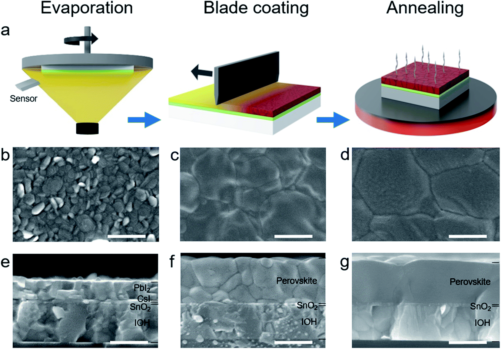 | ||
| Fig. 1 Hybrid PVD/blade coating process for perovskite layers and morphology after each step. (a) Schematic of the three steps of the PVD/blade coating fabrication process. SEM top and cross-section view images after each fabrication step: (b) and (e) after evaporation, (c) and (f) after blade coating and (d) and (g) after thermal annealing. The scale bar is 500 nm. | ||
Morphology and crystallinity of the perovskite film
In Fig. 1b–g, scanning electron microscopy (SEM) images depict the film morphology after each step of the PVD/blade coating process. Additionally, we provide SEM images of CsI layer to unveil its morphology in Fig. S1.† As shown in Fig. 1b the evaporated PbI2 layer is composed of mixed rounded and elliptical plate-shaped grains of around 30 nm to 120 nm size. The cross-section view (Fig. 1e) shows the layer stack with PbI2 (300 nm), CsI (15 nm), SnO2 (35 nm) and hydrogenated indium oxide (IOH, 480 nm). The inorganic halide template has a smooth and uniform morphology, which is beneficial for pinhole-free perovskite films.49 The XRD pattern in Fig. S2† shows a sharp diffraction peak at 12.7°, which corresponds to PbI2.50 After blade coating the organic halide solution, the PbI2 peak decreases and simultaneously, a new diffraction peak at 14.1° emerges, indicating α-phase perovskite even before thermal annealing. Fig. 1c shows the SEM top view of the as-deposited perovskite film, subsequently after the blade coating step. The perovskite grains have a diameter between 100 and 500 nm without voids. The cross-section view (Fig. 1f) shows lots of small grains and the perovskite thickness is approximately twice the thickness of the inorganic halide template.52 After thermal annealing, the grain growth is promoted and it results in large crystal grains and reduced grain boundaries (Fig. 1d).53 In the cross-section view image, the perovskite thickness is unchanged and the surface morphology shows similar roughness to that prior to annealing (Fig. 1g). We further conducted atomic force microscopy (AFM) to quantify the surface roughness of the film after each step (see Fig. S3†). The root mean square roughness (Rq) of the film surface after PVD was calculated to be 8.76 nm (area of 5 × 5 μm2), 30.2 nm after blade coating, and 34.7 nm after thermal annealing. These results agree well with the SEM images.Perovskite film formation mechanism
For two-step methods with compact inorganic template layers (Fig. 2b), obtaining a compact and fully converted perovskite film depends on the processing method and conditions.49,51 For this work, we focus on the processing conditions of the second step – the blade coating. We systematically investigate the organic halide concentration, blade coating speed and substrate temperature to elucidate the influence of these parameters on the perovskite formation mechanism. For these investigations, we fix the gap between the blade and the substrate to 100 μm. First, we use solutions of organic halide precursors (FAI/MABr/MACl) of different concentrations ranging from 10/1/1 to 90/9/9 mg mL−1, while maintaining the substrate temperature at 65 °C and the speed at 30 mm s−1. The results are shown in Fig. 2 and S4.†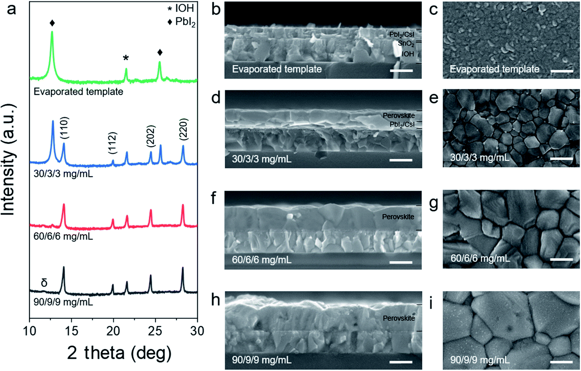 | ||
| Fig. 2 Evaporated inorganic halide template and perovskite films prepared using 30/3/3 mg mL−1, 60/6/6 mg mL−1 and 90/9/9 mg mL−1 of FAI/MABr/MACl organic halide precursor solution concentration. (a) XRD patterns (log-scale) with indicated diffraction peaks of the α-phase perovskite crystal planes. PbI2 is labeled with a ♦ and IOH with a *. (b)–(i) SEM cross-section and top view images of (b) and (c) inorganic halide template and perovskite films prepared with different concentrations of the organic halide precursors: (d) and (e) 30/3/3 mg mL−1, (f) and (g) 60/6/6 mg mL−1 and (h) and (i) 90/9/9 mg mL−1 of FAI/MABr/MACl. The scale bar is 500 nm. | ||
For the solutions of low concentration, 10/1/1 mg mL−1 (Fig. S4a†) and 30/3/3 mg mL−1 (Fig. 2a and S4a†), the highest diffraction peaks correspond to PbI2 (♦), while only tiny peaks can be detected that indicate α-phase perovskite. While the film obtained using 10/1/1 mg mL−1 appears yellowish, the film using 30/3/3 mg mL−1 is brownish, indicating a higher degree of perovskite conversion (Fig. S4b and c†). For both concentrations, we observe that perovskite has formed in the upper region of the film, whereas residual PbI2 is located in the lower region. This perovskite capping layer inhibits further diffusion of organic cations and iodide as well as their reaction with the buried PbI2 (Fig. S5a†),54,55 leading to thinner films (as for higher concentrations). We further spotted bright dots at the grain boundaries (Fig. 2e), which we relate to remnant PbI2. When we use concentrations between 50/5/5 mg mL−1 and 70/7/7 mg mL−1, the film has converted to perovskite, appearing dark brown (Fig. S4d–f†). However, XRD and SEM still show a large amount of unreacted PbI2 for 50/5/5 mg mL−1, while for 60/6/6 mg mL−1 these residues have almost reacted and converted to a compact perovskite layer (Fig. 2f, g and S4e†). We suggest that during the coalescence of perovskite grains, residual PbI2 that is trapped between adjacent perovskite grains reacts with the dissolved organic halide precursors to perovskite and prevents the formation of voids (Fig. S5b†). Using 70/7/7 mg mL−1, the perovskite crystallinity increases and voids are formed (Fig. S4f†). Further increasing the concentration to 90/9/9 mg mL−1 leads to very rough films of large crystal grains (Fig. 2h, i and S4g†). We spot gray dots on the crystal grain surface, which we relate to crystallized organic halides. Furthermore, voids in the bulk and between adjacent grains have formed as no PbI2 was available during coalescence (Fig. S5c†). Additionally, a new diffraction peak appears at 11.8°, indicating a hexagonal perovskite δ-phase (Fig. 2a)56 making this perovskite film inappropriate for PSC devices.
Next, we used different speeds from 1 mm s−1 to 90 mm s−1 and blade coated the organic halide solution on the inorganic halide template, while maintaining the substrate temperature at 65 °C and the concentration at 60/6/6 mg mL−1 (Fig. S6†). For blade coating, two coating regimes exist, the evaporation regime and the Landau–Levich regime.31 In the evaporation regime (speed ≤ 10 mm s−1), slower coating speed yields thicker layers, i.e., a higher amount of organic halide precursors is supplied due to the increased residence time per unit length. Therefore, the diffraction peak of PbI2 decreases with reduced speed (1 mm s−1) and the perovskite peak intensity of (110) increases compared to 10 mm s−1 (Fig. S6a†). The higher perovskite conversion degree can also be observed from the lower transparency of the sample pictures in background illumination mode (Fig. S6b and c†). However, we obtain incomplete perovskite conversion in the evaporation regime. With coating speeds >10 mm s−1, the Landau–Levich regime is reached, where viscous forces become dominant, dragging more solution on the substrate with increasing speed.22 Hence, the degree of perovskite conversion increases with increasing speed. Using a speed of 30 mm s−1, a compact perovskite film with remnant PbI2 is obtained (Fig. S6d†). The sample shows a uniform coating. With a coating speed ≥50 mm s−1, no remnant PbI2 can be detected and the film uniformity is lost. At 50 mm s−1, we observe the formation of voids in the perovskite bulk (Fig. S6e†) and the emergence of a diffraction peak at 11.8°, which indicates δ-phase perovskite (Fig. S6a†). Interestingly, this δ-phase perovskite has been formed immediately after blade coating at 65 °C. Further increasing the speed results in large and coarse crystal grains with high crystallinity (Fig. S6f and g†).
As a consequence, we investigated the influence of different substrate temperatures on the perovskite formation mechanism (Fig. S7†), ranging from 25 °C to 75° (boiling point of isopropanol: 82.5 °C). We maintained the coating speed at 30 mm s−1 and used a concentration of 60/6/6 mg mL−1. For low substrate temperatures ≤40 °C, complete perovskite conversion is obtained, enabled by the slower drying rate. However, the complete conversion comes at the expense of uniformity due to the coffee-ring effect, which also leads to regions of perovskite δ-phase (see the gray area in Fig. S7b and c†). With 55 °C substrate temperature or higher, the coffee-ring effect can be minimized, resulting in uniform coatings. A substrate temperature of 65 °C shows the highest degree of perovskite while maintaining uniformity and high crystallinity (Fig. S7e†). At 75 °C, we observe decreasing perovskite conversion, as the PbI2 diffraction peak increases again. In Fig. S7f,† we also detected remnant PbI2 on the surface of the perovskite film, meaning that the drying rate was too high, interrupting the perovskite conversion on the surface.
To sum up our findings, the perovskite film blade coated with 70 mm s−1 at 65 °C with an organic halide concentration of 60/6/6 mg mL−1 of FAI/MABr/MACl is presented, in Fig. S8,† showing three different regions. We identify these regions as δ-phase perovskite (Fig. S8d,† red), transition (Fig. S8e,† orange) and α-phase perovskite (Fig. S8f,† green) and provide SEM cross-section and top view images for the morphologies. In summary, we have shown that the organic halide precursor concentration, the coating speed and the substrate temperature play important roles in obtaining uniform and converted perovskite films by the PVD/blade process. It is essential to balance the organic and inorganic halide precursors by controlling the processing conditions and selecting an appropriate drying rate to suppress the coffee-ring effect.
Next, we perform depth profiling using time-of-flight secondary ion mass spectroscopy (ToF-SIMS) and X-ray photoelectron spectroscopy (XPS) to shed light on the film composition and the cationic interdiffusion process.
Fig. 3 shows the depth profiles obtained by ToF-SIMS and XPS after each step of the PVD/blade coating process. The ToF-SIMS uses an oxygen sputter gun to detect the positive ion species (Fig. 3a–c). After thermal evaporation, the bilayer inorganic template can be clearly differentiated. First, a constant signal of Pb+ ions (up to 100 s sputter time) is detected, representing the PbI2 layer. Second, a peak of Cs+ ions follows (between 100 and 125 s), indicating the CsI layer, meanwhile the Pb cation signal decreases substantially (Fig. 3a). This agrees well with XPS Cs 3d spectra after PVD (Fig. 3d). The first peaks are detected at a sample depth of 300 nm. After blade coating, a uniform signal of Cs cations is detected across the as-deposited film, which shows that Cs species have already diffused throughout the layer (Fig. 3b). This finding is also supported by XPS in Fig. 3e. After thermal annealing, ToF-SIMS and XPS show comparable results to those after blade coating, which means that perovskite conversion is completed after blade coating and Cs species have diffused uniformly into the perovskite film (Fig. 3c, f and S9†). The subsequent thermal annealing in the PVD/blade coating process finally induces grain growth to reduce the grain boundaries, which is beneficial for the optoelectronic properties.
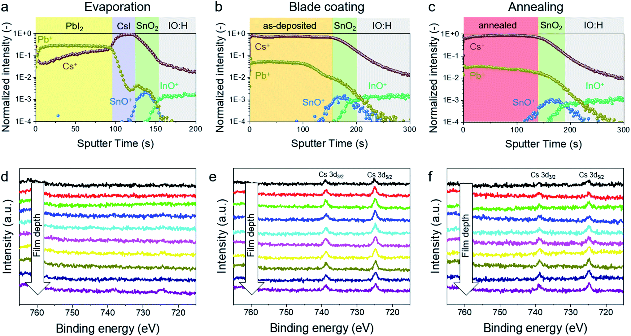 | ||
| Fig. 3 ToF-SIMS depth profile of (a)–(c) cation species at different stages of the hybrid PVD/blade coating process and XPS with depth profiling (d)–(f) of the stack after each step of the coating process. XPS Cs 3d spectra after (a) evaporation, (b) blade coating and (c) annealing. The ten lines correspond to profiles at 0 nm, 10 nm, 20 nm, 30 nm, 40 nm, 80 nm, 120 nm, 160 nm, 200 nm and 300 nm depth. | ||
Optoelectronic properties of the perovskite film
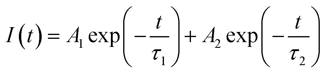
To evaluate the optoelectronic properties of our perovskite film fabricated by PVD/blade, we also fabricated perovskite films by two-step spin coating (spin + spin). To exclude the effect of any charge extraction layer, we deposited the perovskite films directly on quartz substrates. We have shown in Note S1† that the morphology of the evaporated inorganic halide template remains unchanged when using different amorphous substrates.57 Fig. S10a† summarizes the absorbance and the photoluminescence spectra of the perovskite film on a quartz substrate for both fabrication methods (PVD + blade and spin + spin). In Fig. S11,† we provide Tauc plots of these perovskite films and estimated the optical bandgap with a linear fit to be 1.56 eV for both absorbers.58 We further investigated the charge recombination dynamics by steady-state photoluminescence (PL) and time-resolved photoluminescence (TRPL) decay measurements.60 The PL peaks are located at 794 nm (1.56 eV) for both perovskite films. The PL intensity is highest for the perovskite film by PVD/blade, which indicates stronger suppression of non-radiative recombination processes compared to two-step spin coating. Fig. S10b† shows the TRPL decays of the perovskite films by different fabrication methods. We fit the decays with the bi-exponential function:and obtain two decay times, the fast decay lifetime τ1 and the slow decay lifetime τ2.59,61 The fitting parameters are provided in Table S1.† The charge carrier lifetimes are comparably long for both perovskite films by PVD/blade (343 ns and 1406 ns) and spin + spin (396 ns and 1148 ns), showing that perovskite films fabricated by PVD/blade achieve comparable crystal quality and photovoltaic performance (Fig. S12†).
Photovoltaic performance of PSCs by PVD/blade
To evaluate the photovoltaic performance of perovskite films fabricated by PVD/blade, we fabricated n–i–p PSCs with layer stack IOH/SnO2/perovskite/Spiro-OMeTAD/Au on 5 cm × 5 cm substrates. We blade coated both charge transporting layers in ambient air and used non-toxic solvents for both layers, namely de-ionized water for SnO2 and p-xylene for spiro-OMeTAD.62 To passivate the perovskite layer, we used phenethylammonium iodide (PEAI).20Fig. 4a shows a SEM cross-section image of the sample with remnant PbI2, confirmed by XRD (Fig. S13†). J–V measurement of the champion device reveals negligible hysteresis with an open-circuit voltage (VOC) of 1.11 V, a short-current density (JSC) of 23.31 mA cm−2 and a fill factor (FF) of 72.00%, resulting in a PCE of 18.66% (Fig. 4b). The maximum power point (MPP) tracking yields 17.74 mW cm−2 after 30 s (Fig. 4c). This is the highest value for scalable PSCs with green solvents (Fig. 4d). To check the uniformity of our process, we provide photovoltaic performance statistics of 34 cells on 5 cm × 5 cm substrates (Fig. S14†). On average, we obtained a VOC of around 1.13 V and JSC of 21 mA cm−2. The best device showed VOC of 1.16 V for a bandgap of 1.56 eV, being only limited by FF and JSC. The external quantum efficiency (EQE) measurement yields an integrated JSC value of 21.86 mA cm−2, showing further scope of improvement in the light management (Fig. S15†).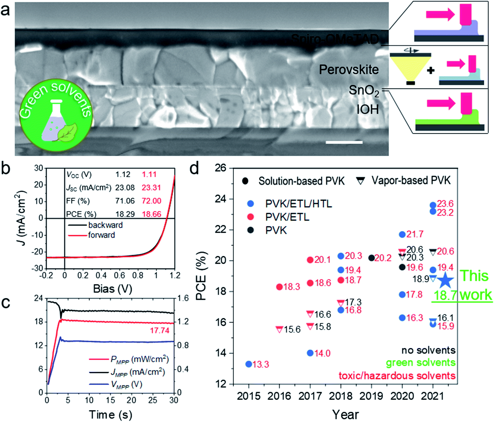 | ||
| Fig. 4 (a) SEM cross-section view of PSC with blade coated charge transporting layers and perovskite layer by PVD/blade coating. The scale bar is 500 nm. (b) Current–voltage behavior and (c) MPP tracking of the champion device. (d) Power conversion efficiency versus year for selected, small-area (∼0.1 cm2) devices with indicated layers fabricated by scalable deposition methods (symbol color). Additionally, devices are distinguished by solution- and vapor-based perovskite absorber layers (symbol type) as well as by the use of green or toxic/hazardous solvents in the perovskite fabrication (font color). Perovskite: PVK, electron transporting layer: ETL and hole transporting layer: HTL. | ||
In conclusion, we have reported a new and scalable hybrid perovskite fabrication process, combining thermal evaporation and blade coating using non-toxic solvents. We systematically investigated the influence of processing parameters on the perovskite formation mechanism during the PVD/blade process and elucidated the growth mechanism. We used such perovskite absorbers together with ambient air-processed, blade coated charge transporting layers to fabricate scalable PSCs with a VOC of 1.16 V and PCE up to 18.7% using green solvents only. With our work, we make an important contribution to reduce the performance gap between toxic and green solvent-based, scalable perovskite fabrication. PVD/blade is a promising process to fabricate high quality perovskite layers on large-area substrates. It can allow a facile implementation of passivation strategies and additives into the precursor solution for blade coating. Additionally, it can be adapted for wide band gap perovskite films and be eventually applied to coat textured surfaces, e.g. in tandem solar cell applications. Moreover, other meniscus-guided deposition methods can replace blade coating, such as slot-die coating or inkjet printing. Overall, the proposed method and its variants are easily scalable for large area manufacturing while the avoidance of toxic solvents is an additional advantage for successful commercialization of the PSC technology. Besides, the processes can be applied on flexible foils as well, paving the way for roll-to-roll or sheet-to-sheet manufacturing in the future.
Conflicts of interest
The authors declare no competing financial interest.Acknowledgements
This work has received funding from the European Union's Horizon 2020 research and innovation program under grant agreement No. 850937 of the PERCISTAND project, the Swiss Federal Office of Energy (SFOE, Project CIGSPSC, grant no. SI/501805-01), and the Swiss National Science Foundation (SNF, Project Bridge Power, grant no. 176552).References
- M. A. Green and K. Emery, Prog. Photovoltaics, 1993, 1(1), 25–29 CAS.
- K. Yoshikawa, H. Kawasaki, W. Yoshida, T. Irie, K. Konishi, K. Nakano, T. Uto, D. Adachi, M. Kanematsu, H. Uzu and K. Yamamoto, Nat. Energy, 2017, 2, 17032 CrossRef CAS.
- S. De Wolf, J. Holovsky, S. J. Moon, P. Löper, B. Niesen, M. Ledinsky, F. J. Haug, J. H. Yum and C. Ballif, J. Phys. Chem. Lett., 2014, 5(6), 1035–1039 CrossRef CAS PubMed.
- G. E. Eperon, S. D. Stranks, C. Menelaou, M. B. Johnston, L. M. Herz and H. J. Snaith, Energy Environ. Sci., 2014, 7(3), 982–988 RSC.
- Q. Dong, Y. Fang, Y. Shao and J. Huang, Science, 2015, 347(6225), 967–970 CrossRef CAS PubMed.
- M. V. Kovalenko, L. Protesescu and M. I. Bodnarchuk, Science, 2017, 358(6364), 745–750 CrossRef CAS PubMed.
- W. J. Yin, T. Shi and Y. Yan, Appl. Phys. Lett., 2014, 104, 063903 CrossRef.
- M. M. Lee, J. Teuscher, T. Miyasaka, T. N. Murakami and H. J. Snaith, Science, 2012, 338(6107), 643–647 CrossRef CAS PubMed.
- R. K. Kothandaraman, Y. Jiang, T. Feurer, A. N. Tiwari and F. Fu, Small Methods, 2020, 4(10), 1–56 CrossRef.
- A. Al-Ashouri, E. Köhnen, B. Li, A. Magomedov, H. Hempel, P. Caprioglio, J. A. Márquez, A. B. M. Vilches, E. Kasparavicius, J. A. Smith, N. Phung, D. Menzel, M. Grischek, L. Kegelmann, D. Skroblin, C. Gollwitzer, T. Malinauskas, M. Jošt, G. Matič, B. Rech, R. Schlatmann, M. Topič, L. Korte, A. Abate, B. Stannowski, D. Neher, M. Stolterfoht, T. Unold, V. Getautis and S. Albrecht, Science, 2020, 370(6522), 1300–1309 CrossRef CAS PubMed.
- B. Chen, S. W. Baek, Y. Hou, E. Aydin, M. De Bastiani, B. Scheffel, A. Proppe, Z. Huang, M. Wei, Y. K. Wang, E. H. Jung, T. G. Allen, E. Van Kerschaver, F. P. García de Arquer, M. I. Saidaminov, S. Hoogland, S. De Wolf and E. H. Sargent, Nat. Commun., 2020, 11, 1257 CrossRef CAS PubMed.
- F. Sahli, J. Werner, B. A. Kamino, M. Bräuninger, R. Monnard, B. Paviet-Salomon, L. Barraud, L. Ding, J. J. Diaz Leon, D. Sacchetto, G. Cattaneo, M. Despeisse, M. Boccard, S. Nicolay, Q. Jeangros, B. Niesen and C. Ballif, Nat. Mater., 2018, 17(9), 820–826 CrossRef CAS PubMed.
- A. Al-Ashouri, A. Magomedov, M. Roß, M. Jošt, M. Talaikis, G. Chistiakova, T. Bertram, J. A. Márquez, E. Köhnen, E. Kasparavičius, S. Levcenco, L. Gil-Escrig, C. J. Hages, R. Schlatmann, B. Rech, T. Malinauskas, T. Unold, C. A. Kaufmann, L. Korte, G. Niaura, V. Getautis and S. Albrecht, Energy Environ. Sci., 2019, 12(11), 3356–3369 RSC.
- D. H. Kim, C. P. Muzzillo, J. Tong, A. F. Palmstrom, B. W. Larson, C. Choi, S. P. Harvey, S. Glynn, J. B. Whitaker, F. Zhang, Z. Li, H. Lu, M. F. A. M. van Hest, J. J. Berry, L. M. Mansfield, Y. Huang, Y. Yan and K. Zhu, Joule, 2019, 3(7), 1734–1745 CrossRef CAS.
- F. Fu, T. Feurer, T. P. Weiss, S. Pisoni, E. Avancini, C. Andres, S. Buecheler and A. N. Tiwari, Nat. Energy, 2017, 2, 16190 CrossRef CAS.
- K. Xiao, R. Lin, Q. Han, Y. Hou, Z. Qin, H. T. Nguyen, J. Wen, M. Wei, V. Yeddu, M. I. Saidaminov, Y. Gao, X. Luo, Y. Wang, H. Gao, C. Zhang, J. Xu, J. Zhu, E. H. Sargent and H. Tan, Nat. Energy, 2020, 5(11), 870–880 CrossRef CAS.
- J. Tong, Z. Song, D. H. Kim, X. Chen, C. Chen, A. F. Palmstrom, P. F. Ndione, M. O. Reese, S. P. Dunfield, O. G. Reid, J. Liu, F. Zhang, S. P. Harvey, Z. Li, S. T. Christensen, G. Teeter, D. Zhao, M. M. Al-Jassim, M. F. A. M. Van Hest, M. C. Beard, S. E. Shaheen, J. J. Berry, Y. Yan and K. Zhu, Science, 2019, 364(6439), 475–479 CrossRef CAS PubMed.
- M. Xiao, F. Huang, W. Huang, Y. Dkhissi, Y. Zhu, J. Etheridge, A. Gray-Weale, U. Bach, Y. B. Cheng and L. Spiccia, Angew. Chem., Int. Ed., 2014, 53(37), 9898–9903 CrossRef CAS PubMed.
- N. J. Jeon, J. H. Noh, Y. C. Kim, W. S. Yang, S. Ryu and S. I. Seok, Nat. Mater., 2014, 13(9), 897–903 CrossRef CAS PubMed.
- Q. Jiang, Y. Zhao, X. Zhang, X. Yang, Y. Chen, Z. Chu, Q. Ye, X. Li, Z. Yin and J. You, Nat. Photonics, 2019, 13(7), 460–466 CrossRef CAS.
- J. Jeong, M. M. Kim, J. Seo, H. Lu, P. Ahlawat, A. Mishra, Y. Yang, M. A. Hope, F. T. Eickemeyer, M. M. Kim, Y. J. Yoon, I. W. Choi, B. P. Darwich, S. J. Choi, Y. Jo, J. H. Lee, B. Walker, S. M. Zakeeruddin, L. Emsley, U. Rothlisberger, A. Hagfeldt, D. S. Kim, M. Grätzel and J. Y. Kim, Nature, 2021, 592, 381–385 CrossRef CAS PubMed.
- X. Gu, L. Shaw, K. Gu, M. F. Toney and Z. Bao, Nat. Commun., 2018, 9, 534 CrossRef PubMed.
- Z. Li, T. R. Klein, D. H. Kim, M. Yang, J. J. Berry, M. F. A. M. Van Hest and K. Zhu, Nat. Rev. Mater., 2018, 3, 1–20 CrossRef CAS.
- D. Li, D. Zhang, K. S. Lim, Y. Hu, Y. Rong, A. Mei, N. G. Park and H. Han, Adv. Funct. Mater., 2020, 2008621 Search PubMed.
- Y. Deng, E. Peng, Y. Shao, Z. Xiao, Q. Dong and J. Huang, Energy Environ. Sci., 2015, 8(5), 1544–1550 RSC.
- S. Razza, F. Di Giacomo, F. Matteocci, L. Cinà, A. L. Palma, S. Casaluci, P. Cameron, A. D’Epifanio, S. Licoccia, A. Reale, T. M. Brown and A. Di Carlo, J. Power Sources, 2015, 277, 286–291 CrossRef CAS.
- K. Hwang, Y. S. Jung, Y. J. Heo, F. H. Scholes, S. E. Watkins, J. Subbiah, D. J. Jones, D. Y. Kim and D. Vak, Adv. Mater., 2015, 27(7), 1241–1247 CrossRef CAS PubMed.
- D. Vak, K. Hwang, A. Faulks, Y. S. Jung, N. Clark, D. Y. Kim, G. J. Wilson and S. E. Watkins, Adv. Energy Mater., 2015, 5(4), 1–8 Search PubMed.
- Z. Wei, H. Chen, K. Yan and S. Yang, Angew. Chem., Int. Ed., 2014, 53(48), 13239–13243 CrossRef CAS PubMed.
- J. H. Heo, M. H. Lee, M. H. Jang and S. H. Im, J. Mater. Chem. A, 2016, 4(45), 17636–17642 RSC.
- Y. Deng, X. Zheng, Y. Bai, Q. Wang, J. Zhao and J. Huang, Nat. Energy, 2018, 3(7), 560–566 CrossRef CAS.
- W. Q. Wu, Z. Yang, P. N. Rudd, Y. Shao, X. Dai, H. Wei, J. Zhao, Y. Fang, Q. Wang, Y. Liu, Y. Deng, X. Xiao, Y. Feng and J. Huang, Sci. Adv., 2019, 5(3), 1–10 Search PubMed.
- F. Di Giacomo, S. Shanmugam, H. Fledderus, B. J. Bruijnaers, W. J. H. Verhees, M. S. Dorenkamper, S. C. Veenstra, W. Qiu, R. Gehlhaar, T. Merckx, T. Aernouts, R. Andriessen and Y. Galagan, Sol. Energy Mater. Sol. Cells, 2018, 181, 53–59 CrossRef CAS.
- S. Tang, Y. Deng, X. Zheng, Y. Bai, Y. Fang, Q. Dong, H. Wei and J. Huang, Adv. Energy Mater., 2017, 7(18), 1–7 CrossRef.
- W. Q. Wu, Q. Wang, Y. Fang, Y. Shao, S. Tang, Y. Deng, H. Lu, Y. Liu, T. Li, Z. Yang, A. Gruverman and J. Huang, Nat. Commun., 2018, 9(1), 1–8 CrossRef PubMed.
- Y. Deng, C. H. van Brackle, X. Dai, J. Zhao, B. Chen and J. Huang, Sci. Adv., 2019, 5(12), 1–9 Search PubMed.
- S. Chen, X. Dai, S. Xu, H. Jiao, L. Zhao and J. Huang, Science, 2021, 373(6557), 902–907 CrossRef CAS PubMed.
- S. Chen, X. Xiao, H. Gu and J. Huang, Sci. Adv., 2021, 7(10), 1–7 Search PubMed.
- National Center for Biotechnology Information, 2-Methoxyethanol – PubChem Compound Summary for CID 8019, accessed Jun 18, 2021, https://pubchem.ncbi.nlm.nih.gov/compound/2-Methoxyethanol.
- National Center for Biotechnology Information, N,N-Dimethylformamide – PubChem Compound Summary for CID 8019, accessed Jun 18, 2021, https://pubchem.ncbi.nlm.nih.gov/compound/6228.
- N. G. Park, Nature Sustainability, 2021, 4(3), 192–193 CrossRef.
- M. Jošt, L. Kegelmann, L. Korte and S. Albrecht, Adv. Energy Mater., 2020, 10, 1904102 CrossRef.
- C. Momblona, L. Gil-Escrig, E. Bandiello, E. M. Hutter, M. Sessolo, K. Lederer, J. Blochwitz-Nimoth and H. J. Bolink, Energy Environ. Sci., 2016, 9(11), 3456–3463 RSC.
- J. Ávila, C. Momblona, P. P. Boix, M. Sessolo and H. J. Bolink, Joule, 2017, 1(3), 431–442 CrossRef.
- E. Köhnen, P. Wagner, F. Lang, A. Cruz, B. Li, M. Roß, M. Jošt, A. B. Morales-Vilches, M. Topič, M. Stolterfoht, D. Neher, L. Korte, B. Rech, R. Schlatmann, B. Stannowski and S. Albrecht, Sol. RRL, 2021, 2100244 CrossRef.
- J. Li, H. Wang, X. Y. Chin, H. A. Dewi, K. Vergeer, T. W. Goh, J. W. M. Lim, J. H. Lew, K. P. Loh, C. Soci, T. C. Sum, H. J. Bolink, N. Mathews, S. Mhaisalkar and A. Bruno, Joule, 2020, 4(5), 1035–1053 CrossRef CAS.
- J. Feng, Y. Jiao, H. Wang, X. Zhu, Y. Sun, M. Du, Y. Cao, D. Yang and S. (Frank) Liu, Energy Environ. Sci., 2021, 14(5), 3035–3043 RSC.
- L. Gil-Escrig, C. Momblona, M. G. La-Placa, P. P. Boix, M. Sessolo and H. J. Bolink, Adv. Energy Mater., 2018, 8(14), 1–6 Search PubMed.
- J. Bing, S. Huang and A. W. Y. Ho-Baillie, Energy Technol., 2020, 8(4), 1–22 Search PubMed.
- T. J. Jacobsson, L. J. Schwan, M. Ottosson, A. Hagfeldt and T. Edvinsson, Inorg. Chem., 2015, 54(22), 10678–10685 CrossRef CAS PubMed.
- H. Ko, S. J. Yang, C. Park, D. H. Sin, H. Lee and K. Cho, ACS Appl. Mater. Interfaces, 2019, 11(7), 7037–7045 CrossRef CAS PubMed.
- D. Liu, M. K. Gangishetty and T. L. Kelly, J. Mater. Chem. A, 2014, 2(46), 19873–19881 RSC.
- A. Ummadisingu and M. Grätzel, Sci. Adv., 2018, 4(2), 1–10 Search PubMed.
- Y. Fu, F. Meng, M. B. Rowley, B. J. Thompson, M. J. Shearer, D. Ma, R. J. Hamers, J. C. Wright and S. Jin, J. Am. Chem. Soc., 2015, 137(17), 5810–5818 CrossRef CAS PubMed.
- M. Chauhan, Y. Zhong, K. Schötz, B. Tripathi, A. Köhler, S. Huettner and F. Panzer, J. Mater. Chem. A, 2020, 8(10), 5086–5094 RSC.
- C. C. Stoumpos, C. D. Malliakas and M. G. Kanatzidis, Inorg. Chem., 2013, 52(15), 9019–9038 CrossRef CAS PubMed.
- F. Fu, L. Kranz, S. Yoon, J. Löckinger, T. Jäger, J. Perrenoud, T. Feurer, C. Gretener, S. Buecheler and A. N. Tiwari, Phys. Status Solidi A, 2015, 212(12), 2708–2717 CrossRef CAS.
- A. R. Zanatta, Sci. Rep., 2019, 9(1), 11225 CrossRef CAS PubMed.
- Y. Yamada, T. Nakamura, M. Endo, A. Wakamiya and Y. Kanemitsu, J. Am. Chem. Soc., 2014, 136(33), 11610–11613 CrossRef CAS PubMed.
- T. Kirchartz, J. A. Márquez, M. Stolterfoht and T. Unold, Adv. Energy Mater., 2020, 10, 1904134 CrossRef CAS.
- K. Liu, Q. Liang, M. Qin, D. Shen, H. Yin, Z. Ren, Y. Zhang, H. Zhang, P. W. K. Fong, Z. Wu, J. Huang, J. Hao, Z. Zheng, S. K. So, C. S. Lee, X. Lu and G. Li, Joule, 2020, 4(11), 2404–2425 CrossRef CAS.
- F. Isabelli, F. Di Giacomo, H. Gorter, F. Brunetti, P. Groen, R. Andriessen and Y. Galagan, ACS Appl. Energy Mater., 2018, 1(11), 6056–6063 CrossRef.
Footnote |
| † Electronic supplementary information (ESI) available: Experimental and characterization methods, additional notes on the inorganic halide template and two-step fabrication methods, XRD patterns, AFM images, EQE spectrum, TOF-SIMS analysis, SEM images, UV-Vis and PL measurements, Tauc and absorption coefficient plots and a table of TRPL lifetimes. See DOI: 10.1039/d1ta07579a |
| This journal is © The Royal Society of Chemistry 2021 |