
An in situ bifacial passivation strategy for flexible perovskite solar module with mechanical robustness by roll-to-roll fabrication†
Hongyu
Wang
a,
Zengqi
Huang
b,
Shuqin
Xiao
a,
Xiangchuan
Meng
b,
Zhi
Xing
b,
Li
Rao
a,
Chenxiang
Gong
b,
Runsheng
Wu
c,
Ting
Hu
 ab,
Licheng
Tan
b,
Xiaotian
Hu
*ab,
Shaohua
Zhang
*a and
Yiwang
Chen
*bd
ab,
Licheng
Tan
b,
Xiaotian
Hu
*ab,
Shaohua
Zhang
*a and
Yiwang
Chen
*bd
aSchool of Materials Science and Engineering, Nanchang University, 999 Xuefu Avenue, Nanchang 330031, China. E-mail: shz@ncu.edu.cn; happyhu@ncu.edu.cn
bCollege of Chemistry, Institute of Polymers and Energy Chemistry, Nanchang University, Nanchang 330031, P. R. China. E-mail: ywchen@ncu.edu.cn
cSchool of New Energy Science and Engineering, Xinyu University, Xinyu 338004, China
dInstitute of Advanced Scientific Research (iASR), Jiangxi Normal University, 99 Ziyang Avenue, Nanchang 330022, China
First published on 26th January 2021
Abstract
The inevitable interfacial defects in the under layer of perovskite films still hinder the power conversion efficiency (PCE) and stability of perovskite solar cells (PSCs), especially of large-area flexible devices up-scaled by roll-to-roll (R2R) technology. Herein, we demonstrate an in situ bifacial passivation strategy via a simple hydroiodic acid (HI) soaking of NiOx-based hole transport layer during R2R printing. Concretely, the trivalent nickel compound on the film surface is reduced to nickel iodide (NiI2) by a HI redox reaction, thereby optimizing the interface contact and ameliorating the work function. Meanwhile, NiI2 coordinates with lead atoms in the perovskite to form a Pb–I bond, which induces the orderly growth of the perovskite lattice and enhances the quality of the crystalline film. Consequently, the PCE of the optimized flexible devices reaches up to 19.04% (1 cm2) and 16.15% (15 cm2). Moreover, the stability and mechanical property of these devices are also improved. This work provides a deep understanding of the NiOx/perovskite interface and an approach for printable interface optimization.
Introduction
In recent years, organic–inorganic halide perovskite solar cells have been developed rapidly as next-generation photovoltaic devices, owing to the rapid improvement in efficiency (over 25%) and long-time stability of PSCs.1–4 Specifically, flexible devices have been extensively studied for their wide application prospects, which has enabled portability and roll-to-roll (R2R) fabrication to be implemented in large-area modules.5–7 Meanwhile, due to the low-temperature processability and efficient photogenerated carrier separation, p–i–n planar structure has been generally adopted in flexible PSCs.8,9 However, there still exist some problems in large-scale flexible PSCs, such as the brittleness of indium tin oxide (ITO) electrode and poor film morphology of the charge transport layer and perovskite layer,10,11 which could significantly reduce the device performance. Up to now, although some PEDOT:PSS electrodes have been developed into large-area flexible PSCs,10,12–16 the work function of these alternatives does not match well with that of the perovskite layer, leading a relatively low open-circuit voltage (Voc).17–20 Thus, a hole transport layer (HTL) is urgently needed to modify the PEDOT:PSS electrode with suitable energy level alignment. Meanwhile, the hole transport layer sandwiched between the photoactive perovskite and charge collection electrode plays a significant role in improving device performance by promoting perovskite crystal growth and optimizing carrier transport.21–24In general, the most widely used hole transport materials in p–i–n flexible perovskite devices are mainly poly (3,4-ethylenedioxythiophene):polystyrene sulfonate (PEDOT:PSS) AI4083,25 poly[bis(4-phenyl)(2,4,6-trimethylphenyl)amine] (PTAA)26 and NiOx.27 However, as organic HTLs, PEDOT:PSS Al4083 and PTAA possess several drawbacks, such as mismatched work function, high cost, and easy degradation in humidity and air.28 These inherent disadvantages limit their application in the R2R production.28,29 By contrast, low-temperature-processed NiOx is regarded as a promising HTL candidate with the superiorities of wide-bandgap, good optical transparency, excellent stability and low cost.30,31 However, due to the poor printability of NiOx and the enrichment of Ni3+ compounds on the surface,32,33 there usually exist many defects on the film surface, which incur hole accumulation near the perovskite interface with trap-assisted nonradiative recombination losses.34 In addition, these defects lead to a rough contact with the perovskite layer, which deteriorates the film morphology and generates more interface defects.35,36 In order to solve the above issues, He et al. applied potassium chloride (KCl) to modify the surface of the NiOx film to improve the ordering of the perovskite crystals at the interface, thereby reducing interface defects and inhibiting charge recombination.37 Park et al. improved the interface contact and passivated interface defects by inserting an organic interlayer between the NiOx and perovskite layers.38 These results indicate that controlling the interface between the NiOx HTL and the perovskite photoactive layer is an effective strategy to passivate interface defects. Due to the complexity of these processes, the application in large-area printing has not been effectively confirmed. Therefore, it is very important to develop an interface passivation technology for large-area printing.
In this work, we demonstrate a simple bifacial passivation strategy at the NiOx-perovskite interface during the R2R printing process. As shown in Fig. 1a, due to the acidity and reducibility of hydroiodic acid (HI), an in situ soaking treatment is performed. The content of Ni3+ compounds enriched on the surface of the NiOx film is greatly reduced, which simultaneously decreases the interface defects and adjusts the work function of NiOx. Meanwhile, the iodide ions (I−) in the reaction product nickel iodide (NiI2) form I–Pb bonds with lead in the perovskite lattice to effectively passivate the I− vacancy defects in the perovskite. Perovskite films with low defects can effectively inhibit interfacial charge recombination and improve charge transfer. With the assistance of the HI treatment and solution shearing during the printing process, flexible perovskite solar cells are fabricated with a champion power conversion efficiency (PCE) of 19.04% (1.01 cm2). Moreover, a 15 cm2 HI-treated PSC module is successfully fabricated via R2R printing (Fig. 1b), which shows a PCE of 16.15% on a flexible substrate with remarkable environmental stability and mechanical robustness. This work provides a new strategy for interface optimization, which provides significant inspiration for the fabrication of high-performance flexible PSCs.
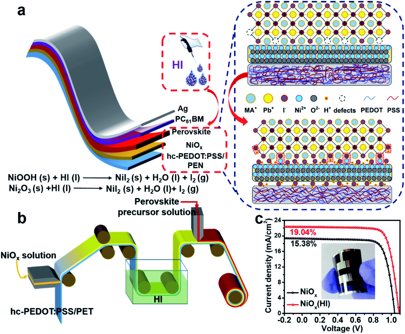 | ||
| Fig. 1 In situ bifacial passivation mechanism and device preparation. (a) Diagram of the passivation mechanism. (b) Fabrication procedure for perovskite solar cells by R2R process. (c) J–V curves of flexible devices (1.01 cm2) with and without HI treatment. Inset presents the photograph of flexible perovskite solar cells. | ||
Results and discussion
To validate the multiple effects of this in situ bifacial passivation, 1.01 cm2 rigid perovskite devices are firstly fabricated by meniscus-coating (Fig. S1, ESI†) with a structure of glass/hc-PEDOT:PSS10/NiOx/perovskite/PC61BM/Ag. During the fabrication of NiOx films, NiOx nanoparticles are induced to evenly deposit on the substrate owing to the shear force of the solution, which could greatly optimize the morphology of the NiOx films as compared with the preparation by spin coating. To further confirm the above theory, atomic force microscopy (AFM) (Fig. S2, ESI†) and optical microscopy (OM) (Fig. S3 and S4, ESI†) characterizations of NiOx films fabricated by the meniscus-coating process and spin-coating process are carried out. The results show that the NiOx films fabricated by the meniscus-coating process are more uniform and there is no obvious aggregation phenomenon. Then, the meniscus-coated NiOx films are treated with HI solution, and the device performance is greatly enhanced from 17.86% (reference) to 20.51% (HI treatment) (Fig. S5, ESI†). Subsequently, the meniscus-coated prototype is extended to the flexible R2R printing system. The R2R printing has been proved to be a mature technology for fabricating large-scale flexible devices.39–43 Thus, we have used the R2R printing technology for further fabricating flexible PSCs.Before R2R printing, the optimal concentration for HI surface modification needs to be explored to maximize device performance. The in situ soaking treatment with HI at concentrations of 0.1 wt%, 0.3 wt%, 0.6 wt% and 0.9 wt%, respectively, is further investigated. The typical J–V curves of the devices with different concentrations of HI soaking treatment are shown in Fig. S6 (ESI†), and the corresponding photovoltaic parameters are summarized in Table S1 (ESI†). The PCE increases significantly with a maximum performance attained when the perovskite films are soaked in a 0.6 wt% HI solution. The device performance begins to drop when the HI concentration further increases to 0.9 wt%, possibly owing to excessive reduction caused by HI. The best PCE of 19.04% for the flexible devices (1.01 cm2) is achieved with 0.6 wt% HI surface treatment under 1-sun condition, along with a Voc as high as 1.09 V, a short-circuit current density (Jsc) of 22.32 mA cm−2 and a fill factor (FF) of 78.26%, that is much higher than 15.38% without HI treatment (Fig. 1c). Therefore, the optimal concentration for HI treatment is defined as 0.6 wt% for the following characterizations.
Effects of HI treatment on NiOx film
To directly investigate the changes in the NiOx films after HI treatment, X-ray photoelectron spectroscopy (XPS) analysis is performed to explore the element composition of the NiOx films. The Ni 2p3/2 characteristic peaks of the NiOx film are shown in Fig. 2a. The background is subtracted from the XPS spectra by using a Shirley-type background subtraction. The fractional peak of the XPS spectrum demonstrates that the Ni 2p spectrum could be well fitted by two different valence states (Ni2+ and Ni3+) in the form of a Gaussian function. Whether in modified or unmodified NiOx films, the remarkable contributor peaks of the Ni3+ state such as in NiOOH (Ni 2p3/2 at 856.0 eV) and Ni2O3 (Ni 2p3/2 at 855.0 eV) and the Ni2+ state as in NiO (Ni 2p3/2 at 853.7 eV) are observed,44–47 which illustrates that the composition of the NiOx film is nonstoichiometric. However, it is important to mention that these Ni3+ state compounds (NiOOH, Ni2O3) can reduce the work function and the transmittance of the NiOx film,48–50 which can greatly degrade its photovoltaic performance. Nevertheless, after the HI treatment on the NiOx film, the compositions of the film are significantly changed, thereby optimizing the film characteristics. Obviously, the characteristic peak area of the Ni3+ state is decreased and that of the Ni2+ state is increased after the HI treatment. As calculated from the integral area in the Ni2p spectrum, the obtained ratio of Ni3+/Ni2+ changes from 3![[thin space (1/6-em)]](https://www.rsc.org/images/entities/char_2009.gif) :2 to 1:1, which indicates that HI interacts with the Ni3+ compounds on the surface of NiOx films.
:2 to 1:1, which indicates that HI interacts with the Ni3+ compounds on the surface of NiOx films.
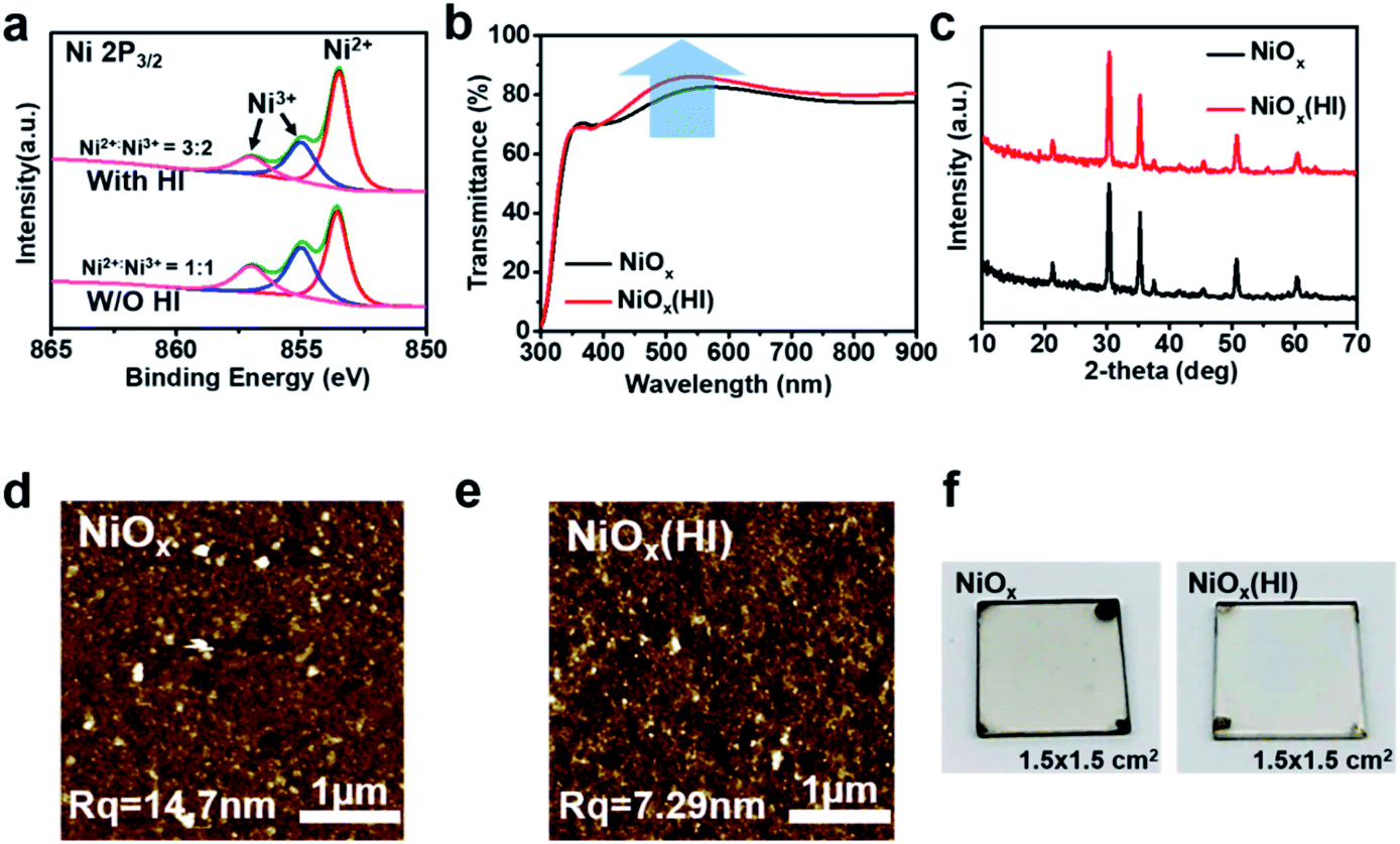 | ||
| Fig. 2 Interface modification of NiOx by HI treatment. (a) High-resolution X-ray photoelectron spectroscopy (XPS) spectra of Ni in the NiOx and NiOx (HI) films. (b) Transmittance spectra of the corresponding NiOx films. (c) X-ray diffraction (XRD) patterns of NiOx film with and without HI treatment. (d and e) The atomic force microscopy (AFM) images of NiOx film with and without HI modification. (f) The photographs of the corresponding NiOx films. | ||
In order to determine the chemical reaction on the surface of the NiOx films treated with HI solution, Gibbs free energy (ΔG) calculation is carried out to judge the progress of the reaction. The corresponding chemical reaction equations in this process are shown as follows:
| Ni(OH)2 (s) + HI (l) → NiI2 (l) + H2O (l) | (1) |
| Ni2O3 (s) + HI (l) → NiI2 (l) + H2O (l) + I2 (g) | (2) |
According to the formula ΔG = ΔH − TΔS, the ΔG of the above reactions are all less than zero, which indicates that the reaction is spontaneous (see detailed explanations about Gibbs free energy calculation of reaction equations in ESI Note 1†). The reduction of Ni3+ compounds in the NiOx films is beneficial to increase the work function of NiOx, which helps to achieve better energy alignment.51 As illustrated in Fig. S7,† the energy levels of the NiOx films with or without HI surface modification are measured with ultraviolet photoelectron spectroscopy (UPS) and the corresponding energy level diagrams of PSCs are drawn. The valence band maximum (VBM) values can be calculated according to the formula VBM = WF + (EF − EVB), where WF is the work function, EF is the Fermi level, and EVB is the valence band energy level.52 The VBM energy (5.34 eV) of the NiOx film with HI surface modification is more aligned with the valence band (5.47 eV) of the perovskite, which is beneficial for hole transporting and electron blocking. To further explore the electrical properties of the NiOx film, the electrical conductivity and surface electrostatic potential are measured. As shown in Fig. S8,† the conductivity of the NiOx film after HI acid surface treatment has been slightly increased from 2.30 × 10⁻⁴ S m−1 to 2.84 × 10⁻⁴ S m−1, which is beneficial to enhance carrier transport and increase the open circuit voltage. Moreover, the surface potential of the NiOx film is measured by Kelvin probe force microscopy (KPFM).
As shown in Fig. S9,† the surface potential of the NiOx film with HI treatment is smaller than that of pristine NiOx film, indicating that the HI surface modification treatment slightly increases the work function of NiOx. This is consistent with the UPS results. Meanwhile, the NiOx films exhibit higher light transmittance in the visible spectrum after HI surface treatment due to the decrease in hydroxides on the surface of the NiOx films. Hydroxyl (–OH) groups are mainly distributed on the surface of the NiOx film to induce interface defects.36,53 As shown in Fig. 2b, the transmittance of PET/hc-PEDOT:PSS/NiOx substrate can be significantly improved in the visible light range after HI surface treatment, which is conducive to enhancing the absorption of photons in the perovskite layer. In addition, since the as-prepared NiOx films are deposited via NiOx nanoparticles, the HI interface modification does not affect the crystallization of NiOx, which can be confirmed by the X-ray diffraction (XRD) patterns (Fig. 2c). From the diffraction pattern, the NiOx is a cubic crystal structure and there is no significant difference in the characteristic peaks before and after HI treatment.
To investigate the changes in NiOx film morphology after HI treatment, the morphology of the NiOx films is examined by using atomic force microscopy (AFM). As shown in Fig. 2d and e, although the NiOx nanoparticles are very small and uniform, the roughness of both NiOx and NiOx (HI) films is still quite large. This may be caused by the easy aggregation of nanoparticles, and this aggregation phenomenon becomes more serious as the printing area increases. However, the NiOx film based on HI surface treatment presents a smooth surface roughness, which could be attributed to the reduction of the surface defect state induced by the hydroxyl (–OH).53 In addition, such a smooth surface is beneficial to reduce the trap state of the interface and enhance the ohmic contact between layers. This result is consistent with the previous analysis. The photographs, as shown in Fig. 2f, further prove that the NiOx film with HI surface treatment is more transparent and smoother, which contributes to improving the light transmittance of the film as well as optimizing the interface contact.
Effects of HI treatment on perovskite film
In addition, for the purpose of exploring whether the interface products can interact with the upper perovskite layer, charge differential density analysis and ab initio molecular dynamics (AIMD) simulation are performed on the interface between NiOx and perovskite layers.54 According to the charge density analysis (Fig. 3a and S10†), the reaction product nickel iodide (NiI2) existing at the interface can interact with the perovskite crystals, resulting in the redistribution of interface charges. As illustrated in Fig. 3a, the charge density of I and Pb element at the interface increases, indicating that the Pb–I bond is formed at the interface. From partial charge density analysis (Fig. 3a), the valence band below the Fermi level is mainly distributed on NiI2, whereas the conduction band above the Fermi level is mainly distributed on the perovskite. Then, AIMD simulation is employed to analyze the stable existence of I–Pb bonds. The simulation model we have chosen is the interface between NiOx (HI) (HI-modified NiOx) and perovskite (001) film, and the system dynamics are evolved at 300 K for several picoseconds. As shown in Fig. 3b, the structure can remain stable at 300 K during the simulation (after 6 ps) without significant distortion of the geometric structure, indicating the high thermodynamic stability of NiI2/perovskite. The potential energy and the temperature are also oscillating near the equilibrium state (Fig. S11†). The first peak of the radical distribution function (RDF) of Ni–I (Fig. S12†) is at 2.72 Å. There is no distribution between the first and second peak, which indicates stable Ni–I bonds. The first peak of RDF of Pb–I (Fig. S12†) is at 3.07 Å, but Pb–I is not always kept stable at the interface. As shown in Fig. S13,† the Pb–I bond length fluctuates between 3.5 to 5 Å, which results in a dynamic equilibrium at the interface. Obviously, the stable I–Pb bond formed at the interface can stabilize the perovskite lattice and inhibit the decomposition of the perovskite and the formation of vacancy defects, which is beneficial to reduce the defect states of the interface to facilitate the extraction and transport of charge carriers, thereby optimizing the photovoltaic performance of the flexible device.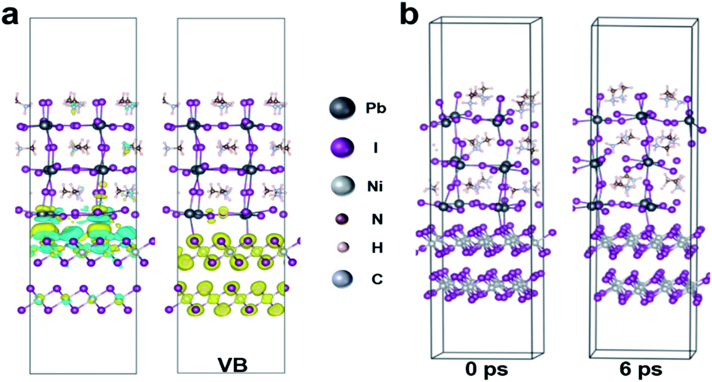 | ||
| Fig. 3 The Interface interaction between NiOx (HI) and perovskite films. (a) Charge differential density analysis of the interfaces. (b) Ab initio molecular dynamics (AIMD) of the interaction between NiI2 and perovskite. For simplifying the calculation, MAPbI3 perovskite supercell is used for AIMD simulation. | ||
In order to further detect the influence of this interaction effect on the perovskite film, the resulted perovskite films deposited on different NiOx films are characterized. The perovskite films are deposited by using a continuous R2R process and sequentially annealed at 100 °C for 30 min in a low dew point condition. The cross-section scanning electron microscopy (SEM) and atomic force microscopy (AFM) are conducted to investigate the effect of NiI2 on the perovskite film morphology and quality. As shown in Fig. 4a and S14,† a high-quality perovskite film composed of large grains and super-compact device structure is obtained upon the NiOx film with HI treatment, while the reference perovskite film exhibits small grains with more grain boundaries. More interestingly, the optimized perovskite crystal growth has an obvious vertical orientation. The average grain size of the perovskite films is increased from 185 nm to 336 nm after HI interface treatment (Fig. S15, ESI†), which could be ascribed to the influence of the formation of Pb–I bond on perovskite crystallization at the interface. The formation of Pb–I bond at the interface helps to induce the nucleation and directional growth of the perovskite at the interface, which leads to an increase in the size of the perovskite grains and the formation of dense perovskite films with high crystallinity.54 In order to further explore the crystal growth of the corresponding perovskite films, 2D grazing-incidence wide-angle X-ray scattering (GIWAXS) is measured to study the crystal characteristics of the perovskite films. As shown in Fig. 4b, the (110) diffraction peak of the perovskite based on NiOx (HI) layer is significantly enhanced as compared with that of the control film, which corresponds with the results of XRD measurements (Fig. S16, ESI†). In addition, the standard diffraction peak intensity of PbI2 at 2θ = 12.67° is missing in the perovskite film based on NiOx (HI) layer, which indicates that the formation of I–Pb bonds at the interface can effectively improve the quality of the perovskite film and inhibit the degradation of the perovskite.55 Meanwhile, the optimized perovskite film also helps to improve the photon collection of the flexible devices, which leads to a stronger absorption in the UV-vis spectra (Fig. 4c). Steady-state photoluminescence (PL) and time-resolved photoluminescence (TRPL) spectroscopy measurements are further employed to investigate the effect of NiI2 defect passivation on the carrier dynamics at the interface. As shown in Fig. 4c, the lower fluorescence intensity of the samples based on NiOx (HI) layer indicates that the charge carriers are effectively extracted and the non-radiative recombination loss at the interface is significantly reduced. Similar results are revealed in the TRPL spectra (see in Fig. 4d). The perovskite films based on NiOx (HI) layer yield a shorter carrier recombination lifetime than the reference (23 ns versus 35 ns). These results could indicate that the photogenerated hole from the perovskite layer can be effectively extracted and transferred to the anode with an ideal ohmic contact.56 More importantly, the significant decrease observed in the PL intensity and TRPL decay time could be caused by the passivation of interface defects. In general, the deep-level defects at the surface of polycrystalline perovskite films, such as iodine vacancies, could become the non-radiative recombination centers of charge carriers. These defects may result in Voc losses,57,58 which will reduce the device performance. Interestingly, the excess iodide ions remaining at the interface can effectively fill in the iodine vacancy by HI treatment, thereby passivating perovskite interface defects and suppressing non-radiative carrier recombination.
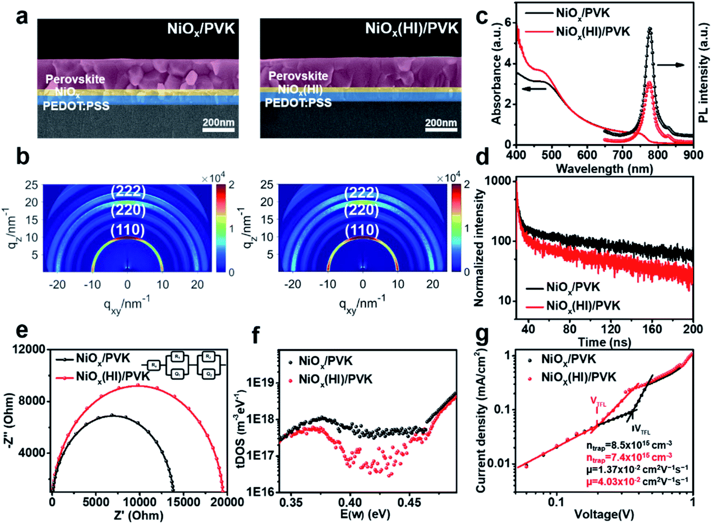 | ||
| Fig. 4 Crystallization and quality of flexible perovskite films based on the NiOx films with and without HI treatment. (a) Cross-section SEM images of the PEDOT:PSS/NiOx/PVK layers. (b) 2D GIWAXS scattering patterns for the corresponding perovskite films. (c) UV-vis absorption spectra and steady-state PL spectra of the corresponding perovskite films. (d) Time-resolved photoluminescence (TRPL) of perovskite films. (e) The typical Nyquist plots of the corresponding PSCs. (f) Trap density of states (tDOS) spectra for the corresponding PSCs. (g) The space-charge-limited-current (SCLC) module for NiOx and NiOx (HI) hole-only devices. | ||
To better understand the charge carrier recombination and the distribution of defects, the electrochemical impedance spectroscopy (EIS) of the corresponding devices with an applied potential of 0.8 V under dark conditions over a frequency range of 100 MHz to 4 MHz is conducted. The Nyquist plots for the devices with and without HI interface treatment are shown in Fig. 4e. The larger semicircle corresponding to the devices with HI interface treatment demonstrates a larger recombination resistance, which indicates a lower carrier recombination rate due to the in situ bifacial passivation of NiI2. Furthermore, the carrier trap density and mobility of various perovskite films are also explored. Fig. 4f describes that the devices based on NiOx (HI) layer have lower trap density of states (tDOS) almost over the whole trap depth region, which confirms the beneficial role of HI interface treatment in reducing the deep defects. The I–V response of the crystals in the space-charge-limited-current (SCLC) regime is also measured (Fig. 4g). According to the characteristic I–V trace, the carrier trap density of the device based on HI-treated NiOx layer is calculated to be about 7.4 × 1015 cm−3, which is much lower than that of the reference device (about 8.5 × 1015 cm−3). The carrier mobility shows a similar trend, which increases from 1.37 × 10⁻² cm2 V−1 s−1 to 4.03 × 10⁻² cm2 V−1 s−1. These results are consistent with the previous analysis. The efficient charge extraction and transfer, as well as fewer interface defects, are mainly derived from the high-quality perovskite films and in situ bifacial passivation of NiI2 at the interface.
Characterization of device performance and module design
To validate the influence of the in situ bifacial passivation strategy on photovoltaic performance, the hysteresis phenomenon is then studied. As shown in Fig. 5a and Table S1,† the pristine device exhibits a typical J–V hysteresis, where inferior PCEs of 15.38% and 14.15% appear in forward scan (FS) and reverse scan (RS), respectively. By contrast, champion PCEs of 19.04% (RS) and 18.80% (FS) are obtained for the HI-treated devices, which shows negligible hysteresis. Moreover, the corresponding external quantum efficiency (EQE) spectra (Fig. 5a) of these champion devices exhibit an improvement in the integration current. The corresponding integrated Jsc is in good agreement with the value obtained from the J–V curves. To further describe the continuous output of the HI-treated devices, stabilized photocurrent is measured at a bias voltage of 0.88 V. These devices deliver a stabilized photocurrent of 22.1 mA cm−2 and a stabilized output power of 18.92% after 600 s of continuous irradiation (Fig. 5c). Besides, 100 samples for each device are fabricated to explore the efficiency and reproducibility. The efficiency histogram is combined with the Gaussian fitting. As illustrated in Fig. 5d and e, the devices based on HI treatment show favourable reliability with narrower PCE distribution, and the averaged PCE shows an obvious enhancement from 14.20% (reference) to 18.50% (HI treatment). The satisfactory performance and reproducibility can be attributed to the defect passivation of NiI2 and high-quality PVK films. Furthermore, in order to prove that the defect passivation of NiI2 inhibits carrier recombination at the interface, the dark current voltage characteristics of the corresponding devices are measured. As shown in Fig. S17 (ESI†), the device based on HI treatment has a lower dark current density, which suggests that more photogenerated carriers can be efficiently transmitted instead of direct shunting, resulting in suppressed charge carrier recombination and leakage current.59,60 In addition, the details of carrier recombination are further investigated by measuring the J–V curves under various illumination intensities (see in Fig. S18, ESI†). The interface recombination of devices based on HI treatment is significantly reduced, which is consistent with the above analysis. These results indicate that HI interface treatment can reduce trap-assisted and bimolecular recombination due to the improvement in the perovskite film quality and interfacial contact. In view of the excellent performance of small-area flexible devices, the large-area module based on R2R printing is designed, the corresponding photograph and device structure are shown in the Fig. 5f and g, respectively. The 5 × 5 cm2 module is composed of six sub-cells in series (see in Fig. S19†), which occupies an effective area of 15 cm2 (Fig. S20†). The I–V curve of the flexible module based on NiOx (HI) is shown in Fig. 5h with a high PCE of 16.15% and a maximum power of 242.3 mW. More importantly, the HI interface treatment is compatible with R2R printing, thereby realizing a continuous printing process.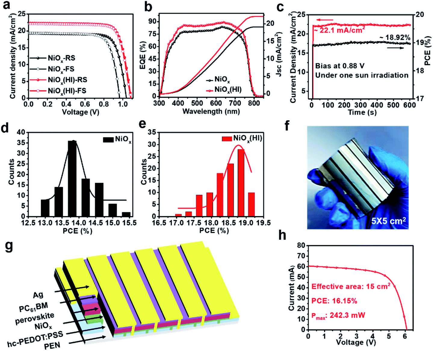 | ||
| Fig. 5 Device performance of PSCs based on NiOx and NiOx (HI) HTLs. (a) J–V curves of flexible PSCs measured in the reverse and forward directions. (b) EQE spectra and integrated Jsc curves of flexible PSCs. (c) Steady-state PCE and current of flexible PSCs at the voltage near the maximum power point. (d and e) Performance distribution of the flexible PSCs. (f) Photograph of the flexible perovskite solar module. (g) The structure of the six section series connected large-area flexible PSCMs. (h) I–V curve of the flexible module based on NiOx (HI) HTL. | ||
Long-term and mechanical stability of the flexible devices
According to literature reports, perovskite devices suffer from severe degradation during operation due to external environmental pressures,60 and this process is usually fatal to the stability of large-area modules. Thus, we have systematically examined the unencapsulated module with and without HI treatment to help understand the operational stability. As presented in Fig. 6a, the long-term stability of the corresponding flexible modules has been evaluated. These modules are stored in air conditions (relative humidity of 30% and 25 °C) without encapsulation. The HI-treated devices exhibit excellent stability; they retain over 80% of the original PCE value after 30 days of degradation. In contrast, the devices without HI treatment maintain only 30% of the initial efficiency. The enhancement of device stability could benefit from the in situ bifacial passivation of NiI2 and the compact perovskite film with fewer grain boundaries, which could effectively suppress device degradation caused by ion migration. To further explore the mechanism of degradation inside the device, time-of-flight secondary ion mass spectroscopy (ToF-SIMS) is employed to detect elemental distribution with aging time. The depth profiles of the reference and the HI-treated devices after storage in ambient conditions for 30 days are shown in Fig. 6b and c, respectively. The I− ions of the devices without HI treatment diffuse obviously much deeper into the NiOx and top silver electrode than those of the devices based on HI treatment. This result further suggests that fewer interface defects and optimized perovskite films are beneficial to inhibit the migration of iodide ions between layers. In addition, the mechanical stability of flexible devices is studied by bending at various curvature radii (from flat to 3 mm). The bending photos of flexible devices under different bending radii are shown in Fig. S21.† As shown in Fig. 6d, the comparison demonstrates that the HI-treated flexible devices exhibit a better bending resistance after 500 bending cycles, which maintain over 80% of the original PCE value under a 3 mm bending radius. Moreover, the normalized PCE for the corresponding devices with different bending cycles at a bending radius of 3 mm is measured, as presented in Fig. 6e. After 5000 bending cycles, the devices based on the HI-treated NiOx layers still retain more than 80% of the original PCE value, but the reference devices are damaged, which correspond with the SEM image analysis (Fig. S22†). These evidences show that the HI interface treatment can effectively improve the mechanical stability of the device, which is mainly attributed to the fact that in situ bifacial passivation of NiI2 reduces the intrinsic stress caused by defects in the film.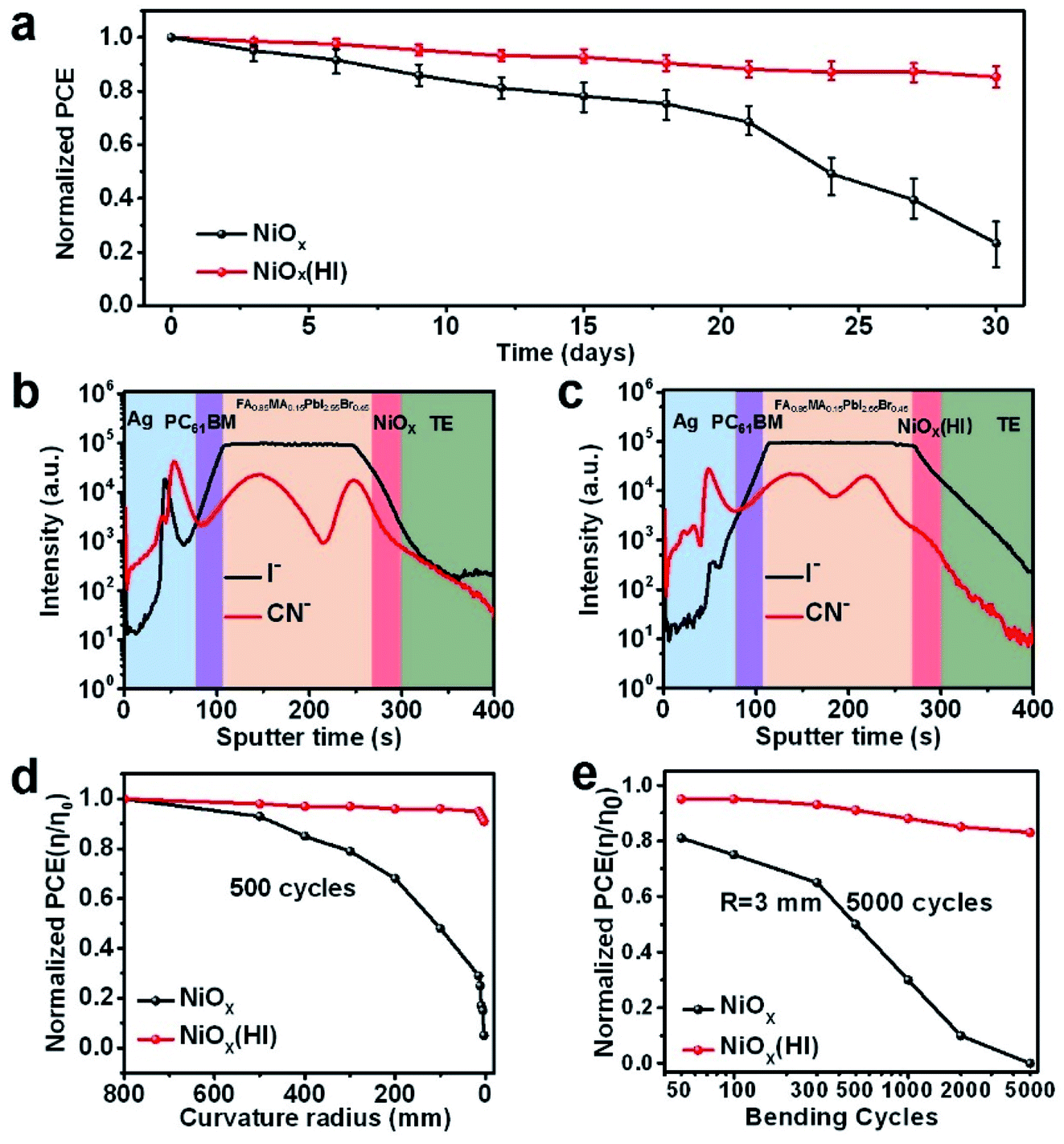 | ||
| Fig. 6 Stability evaluation of large-area flexible module. (a) Normalized PCE of encapsulated PSCs based on NiOx and NiOx (HI) hole-transport layers under ambient condition (25–55% relative humidity and 25–35 °C) for 30 days. ToF-SIMS elemental depth profiles of devices based on (b) NiOx and (c) NiOx (HI) hole-transport layers. (d) Normalized averaged PCE of flexible PSCs chips measured after 500 bending cycles within a curvature radius. (e) Normalized averaged PCE of PSC chips as a function of bending cycles with radius of 3 mm. | ||
Conclusions
In summary, the maximized collocation between NiOx and perovskite has been realized via HI interface treatment. The introduction of HI treatment can effectively reduce the trivalent compounds to NiI2 on the surface of NiOx films, thereby increasing the work function of NiOx and passivating the surface defects. At the same time, the iodine in the reaction product NiI2 can coordinate with the lead in the perovskite to passivate deep-level defects and stabilize the perovskite lattice, thereby reducing the interface defect states and inhibiting the recombination of carriers. The formation of Pb–I bonds at the interface can induce the orderly growth of perovskite grains, thereby increasing the grain size and optimizing the morphology of the film. Better level matching, fewer interface defects, and high-quality perovskite films result in high-performance flexible perovskite devices. Finally, we have fabricated flexible devices by R2R printing and have achieved a high PCE of 19.04% for 1.01 cm2 flexible PSCs and 16.15% for a 15 cm2 solar module with negligible hysteresis. These flexible devices also present excellent bending resistance and long-term stability. The positive effects brought by the HI treatment are promising for pursuing high-performance and stable large area perovskite solar cell modules. This strategy provides an effective approach for the future development of scalable perovskite electronics.Author contributions
Y. C., X. H. and S. Z. conceived and designed the experiments. H. W., Z. H. and S. X. contributed equally to this work. H. W., Z. H. and X. M. fabricated the devices and measured the photovoltaic parameters. Z. X., S. X. and R. W. conducted the finite element simulation. L. R. and C. G. conducted the AFM measurements. L. T. and H. W. carried out the spectrum analysis. H. W., X. H. and Y. C. wrote the manuscript. All authors contributed to the data analysis, discussed the results and commented on the manuscript.Conflicts of interest
There are no conflicts to declare.Acknowledgements
Y. C., S. X. and X. H. thank the support from the National Natural Science Foundation of China (NSFC) (51673091, 51833004, 22005131, 51963016, U1801256, and 51425304).Notes and references
- Q. Dong, Y. Fang, Y. Shao, P. Mulligan, J. Qiu, L. Cao and J. Huang, Science, 2015, 347, 967–970 CrossRef CAS.
- H. Zhou, Q. Chen, G. Li, S. Luo, T. Song, H. Duan, Z. Hong, J. You, Y. Liu and Y. Yang, Science, 2014, 345, 542–546 CrossRef CAS.
- H. Chen, T. Liu, P. Zhou, S. Li, J. Ren, H. He, J. Wang, N. Wang and S. Guo, Adv. Mater., 2019, 32, 1905661 CrossRef.
- K. Huang, Y. Peng, Y. Gao, J. Shi, H. Li, X. Mo, H. Huang, Y. Gao, L. Ding and J. Yang, Adv. Energy Mater., 2019, 9, 1901419 CrossRef CAS.
- T. Bu, J. Li, F. Zheng, W. Chen, X. Wen, Z. Ku, Y. Peng, J. Zhong, Y. Cheng and F. Huang, Nat. Commun., 2018, 9, 4609 CrossRef.
- Y. Y. Kim, T. Yang, R. Suhonen, M. Välimäki, T. Maaninen, A. Kemppainen, N. J. Jeon and J. Seo, Adv. Sci., 2019, 6, 1802094 CrossRef.
- J. Kim, S. Kim, C. Zuo, M. Gao, D. Vak and D. Y. Kim, Adv. Funct. Mater., 2019, 29, 1809194 CrossRef.
- H. Chen, Q. Wei, M. I. Saidaminov, F. Wang, A. Johnston, Y. Hou, Z. Peng, K. Xu, W. Zhou, Z. Liu, L. Qiao, X. Wang, S. Xu, J. Li, R. Long, Y. Ke, E. H. Sargent and Z. Ning, Adv. Mater., 2019, 31, 1903559 CrossRef CAS.
- Q. Xue, M. Liu, Z. Li, L. Yan, Z. Hu, J. Zhou, W. Li, X. Jiang, B. Xu, F. Huang, Y. Li, H.-L. Yip and Y. Cao, Adv. Funct. Mater., 2018, 28, 1707444 CrossRef.
- X. Hu, X. Meng, L. Zhang, Y. Zhang, Z. Cai, Z. Huang, M. Su, Y. Wang, M. Li, F. Li, X. Yao, F. Wang, W. Ma, Y. Chen and Y. Song, Joule, 2019, 3, 1–14 CrossRef.
- Z. Liu, S. Li, X. Wang, Y. Cui, Y. Qin, S. Leng, Y. Xu, K. Yao and H. Huang, Nano Energy, 2019, 62, 734 CrossRef CAS.
- X. Fan, W. Nie, H. Tsai, N. Wang, H. Huang, Y. Cheng, R. Wen, L. Ma, F. Yan and Y. Xia, Adv. Sci., 2019, 6, 1900813 CrossRef CAS.
- Y. Xia, K. Sun and J. Ouyang, Adv. Mater., 2012, 24, 2436 CrossRef CAS.
- N. Kim, S. Kee, S. H. Lee, B. H. Lee, Y. H. Kahng, Y.-R. Jo, B.-J. Kim and K. Lee, Adv. Mater., 2014, 26, 2268 CrossRef CAS.
- N. Kim, H. Kang, J.-H. Lee, S. Kee, S. H. Lee and K. Lee, Adv. Mater., 2015, 27, 2317 CrossRef CAS.
- X. Fan, B. Xu, S. Liu, C. Cui, J. Wang and F. Yan, ACS Appl. Mater. Interfaces, 2016, 8, 14029 CrossRef CAS.
- Y. Zhang, L. Chen, X. Hu, L. Zhang and Y. Chen, Sci. Rep., 2015, 5, 12839 CrossRef CAS.
- X. Hu, Z. Huang, X. Zhou, P. Li, Y. Wang, Z. Huang, M. Su, W. Ren, F. Li, M. Li, Y. Chen and Y. Song, Adv. Mater., 2017, 29, 1703236 CrossRef.
- S. Allard, M. Forster, B. Souharce, H. Thiem and U. Scherf, Angew. Chem., Int. Ed., 2008, 47, 4070 CrossRef CAS.
- C. Zuo and L. Ding, Adv. Energy Mater., 2017, 7, 1601193 CrossRef.
- C. Shen, Y. Wu, H. Zhang, E. Li, W. Zhang, X. Xu, W. Wu, H. Tian and W. Zhu, Angew. Chem., Int. Ed., 2019, 58, 11593 Search PubMed.
- S. Ye, H. Rao, W. Yan, Y. Li, W. Sun, H. Peng, Z. Liu, Z. Bian, Y. Li and C. Huang, Adv. Mater., 2016, 28, 9648 CrossRef CAS.
- L. Calió, S. Kazim, M. Grätzel and S. Ahmad, Angew. Chem., Int. Ed., 2016, 55, 14522 CrossRef.
- J. Shi, X. Xu, D. Li and Q. Meng, Small, 2015, 11, 2472 CrossRef CAS.
- H. Elbohy, B. Bahrami, S. Mabrouk, K. M. Reza, A. Gurung, R. Pathak, M. Liang, Q. Qiao and K. Zhu, Adv. Funct. Mater., 2019, 29, 1806740 CrossRef CAS.
- S. Zhang, M. Stolterfoht, A. Armin, Q. Lin, F. Zu, J. Sobus, H. Jin, N. Koch, P. Meredith, P. L. Burn and D. Neher, ACS Appl. Mater. Interfaces, 2018, 10, 21681 CrossRef CAS.
- J. H. Kim, P. Liang, S. T. Williams, N. Cho, C. C. Chueh, M. S. Glaz, D. S. Ginger and A. K. Y. Jen, Adv. Mater., 2015, 27, 695 CrossRef CAS.
- S. Sajid, A. M. Elseman, H. Huang, J. Ji, S. Dou, H. Jiang, X. Liu, D. Wei, P. Cui and M. Li, Nano Energy, 2018, 51, 408 CrossRef CAS.
- X. Yin, P. Chen, M. Que, Y. Xing, W. Que and C. Niu, ACS Nano, 2016, 10, 3630 CrossRef CAS.
- W. Chen, F. Liu, X. Feng, A. B. Djurišić, W. Chan and Z. He, Adv. Energy Mater., 2017, 7, 1700722 CrossRef.
- J. R. Manders, S. W. Tsang, M. J. Hartel, T. Lai, S. Chen, C. M. Amb, J. R. Reynolds and F. So, Adv. Funct. Mater., 2013, 23, 2993 CrossRef CAS.
- H. Zhang, J. Cheng, F. Lin, H. He, J. Mao, K. S. Wong, A. K.-Y. Jen and W. C. H. Choy, ACS Nano, 2016, 10, 1503 CrossRef CAS.
- W. Chen, Y. Wu, J. Liu, C. Qin, X. Yang, A. Islam, Y. Cheng and L. Han, Energy Environ. Sci., 2015, 8, 629 RSC.
- H. Zhang, X. Ren, X. Chen, J. Mao, J. Cheng, Y. Zhao, Y. Liu, J. Milicc, W. Yin, M. Grätzelc and W. C. H. Choy, Energy Environ. Sci., 2018, 11, 2253 RSC.
- W. Wu, P. N. Rudd, Z. Ni, C. H. V. Brackle, H. Wei, Q. Wang, B. R. Ecker, Y. Gao and J. Huang, J. Am. Chem. Soc., 2020, 142, 3989 CrossRef CAS.
- W. Yang, B. W. Park, E. H. Jung, N. J. Jeon, Y. C. Kim, D. U. Lee, S. S. Shin, J. W. Seo, E. K. Kim, J. H. Noh and S. I. Seok, Science, 2017, 356, 1376–1379 CrossRef CAS.
- W. Chen, Y. Zhou, G. Chen, Y. Wu, B. Tu, F. Liu, L. Huang, A. M. C. Ng, A. B. Djurišić and Z. He, Adv. Energy Mater., 2019, 9, 1803872 CrossRef.
- Z. Li, B. H. Jo, S. J. Hwang, T. H. Kim, S. Somasundaram, E. Kamaraj, J. Bang, T. K. Ahn, S. Park and H. J. Park, Adv. Sci., 2019, 6, 1802163 CrossRef.
- J. E. Kim, S. S. Kim, C. Zuo, M. Gao, D. Vak and D. Y. Kim, Adv. Funct. Mater., 2019, 29, 1809194 CrossRef.
- B. Dou, J. B. Whitaker, K. Bruening, D. T. Moore, L. M. Wheeler, J. Ryter, N. J. Breslin, J. J. Berry, S. M. Garner, F. S. Barnes, S. E. Shaheen, C. J. Tassone and K. Zhu, ACS Energy Lett., 2018, 3, 2558 CrossRef CAS.
- C. Gong, S. Tong, K. Huang, H. Li, H. Huang, J. Zhang and J. Yang, Sol. RRL, 2020, 4, 1900204 CrossRef CAS.
- Q. Hu, H. Wu, J. Sun, D. Yan, Y. Gao and J. Yang, Nanoscale, 2016, 8, 5350 RSC.
- C. Zuo, D. Vaka, D. Angmoa, L. Ding and M. Gao, Nano Energy, 2018, 46, 185 CrossRef CAS.
- X. Fan, W. Nie, H. Tsai, N. Wang, H. Huang, Y. Cheng, R. Wen, L. Ma, F. Yan and Y. Xia, Adv. Sci., 2019, 6, 1900813 CrossRef CAS.
- W. J. Scheideler, N. Rolston, O. Zhao, J. Zhang and R. H. Dauskardt, Adv. Energy Mater., 2019, 9, 1803600 CrossRef.
- M. I. Saidaminov, J. Kim, A. Jain, R. Q-Bermudez, H. Tan, G. Long, F. Tan, A. Johnston, Y. Zhao, O. Voznyy and E. H. Sargent, Nat. Energy, 2018, 3, 648 CrossRef CAS.
- D. Barboni and R. A. De Souza, Energy Environ. Sci., 2018, 11, 3266 RSC.
- R. Islam, G. Chen, P. Ramesh, J. Suh, N. Fuchigami, D. Lee, K. A. Littau, K. Weiner, R. T. Collins and K. C. Saraswat, ACS Appl. Mater. Interfaces, 2017, 9, 17201 CrossRef CAS.
- Z. Gao, Y. Wang, D. Ouyang, H. Liu, Z. Huang, J. Kim and W. C. H. Choy, Small Methods, 2020, 4, 2000478 CrossRef.
- Y. Zhao, H. Zhang, X. Ren, H. L. Zhu, Z. Huang, F. Ye, D. Ouyang, K. W. Cheah, A. K.-Y. Jen and W. C. H. Choy, ACS Energy Lett., 2018, 3, 2891 CrossRef CAS.
- F. Jiang, W. C. H. Choy, X. Li, D. Zhang and J. Cheng, Adv. Mater., 2015, 27, 2930 CrossRef CAS.
- L. Zhou, X. Guo, Z. Lin, J. Ma, J. Su, Z. Hu, C. Zhang, S. Frank Liu, J. Chang and Y. Hao, Nano Energy, 2019, 60, 583 CrossRef CAS.
- I. J. Park, G. Kang, M. A. Park, J. S. Kim, S. W. Seo, D. H. Kim, K. Zhu, T. Park and J. Y. Kim, ChemSusChem, 2017, 10, 2660 CrossRef CAS.
- F. Wang, H. Yu, H. Xu and N. Zhao, Adv. Funct. Mater., 2014, 25, 1120 CrossRef.
- W. Li, W. Zhang, S. V. Reenen, R. J. Sutton, J. D. Fan, A. A. Haghighirad, M. B. Johnston, L. Wang and H. J. Snaith, Energy Environ. Sci., 2016, 9, 490–498 RSC.
- H. Abdy, A. Aletayyeb, M. Kolahdouz and E. A. Soleimani, AIP Adv., 2019, 9, 015216 CrossRef.
- F. Li, X. Deng, F. Qi, Z. Li, D. Liu, D. Shen, M. Qin, S. Wu, F. Lin, S. Jang, J. Zhang, X. Lu, D. Lei, C.-S. Lee, Z. Zhu and A. K.-Y. Jen, J. Am. Chem. Soc., 2020, 142, 20134–20142 CrossRef CAS.
- H. D. Kim, N. Yanagawa, A. Shimazaki, M. Endo, A. Wakamiya, H. Ohkita, H. Benten and S. Ito, ACS Appl. Mater. Interfaces, 2017, 9, 19988 CrossRef CAS.
- G. -J. A. H. Wetzelaer, M. Scheepers, A. M. Sempere, C. Momblona, J. Ávila and H. J. Bolink, Adv. Mater., 2015, 27, 1837 CrossRef CAS.
- J. Bisquert and E. J. Juarez-Perez, J. Phys. Chem. Lett., 2019, 10, 5889 CrossRef CAS.
Footnote |
| † Electronic supplementary information (ESI) available. See DOI: 10.1039/d0ta12067g |
| This journal is © The Royal Society of Chemistry 2021 |