
 Open Access Article
 This Open Access Article is licensed under a Creative Commons Attribution-Non Commercial 3.0 Unported Licence
Influence of the stoichiometry of tin-based 2D/3D perovskite active layers on solar cell performance†
Shuyan
Shao‡
*a,
Maykel
Nijenhuis‡
a,
Jingjin
Dong
b,
Simon
Kahmann
 a,
Gert H.
ten Brink
c,
Giuseppe
Portale
b and
Maria Antonietta
Loi
*a
a,
Gert H.
ten Brink
c,
Giuseppe
Portale
b and
Maria Antonietta
Loi
*a
aPhotophysics and OptoElectronics, Zernike Institute for Advanced Materials, University of Groningen, Nijenborgh 4, 9747 AG, The Netherlands. E-mail: s.shao@rug.nl; m.a.loi@rug.nl
bMacromolecular Chemistry and New Polymeric Material, Zernike Institute for Advanced Materials, University of Groningen, Nijenborgh 4, 9747 AG, The Netherlands
cNanostructured Materials and Interfaces, Zernike Institute for Advanced Materials, University of Groningen, Nijenborgh 4, 9747 AG, The Netherlands
First published on 30th March 2021
Abstract
2D/3D mixed tin perovskites have the advantages of high crystallinity and preferential orientation compared to pure 3D tin perovskite. However, solar cells based on 2D/3D mixed tin perovskites are still limited by low power conversion efficiency (PCE) when compared to their lead-based counterparts. It is essential to gain deeper insight into the factors that limit the performance of these solar cells in order to further improve them. In this work, we demonstrate that the starting stoichiometry of 2D/3D (PEA0.08FAxSnI3) tin perovskite films influences their crystallization and photophysical properties as well as the solar cell performance. The reference 2D/3D film (x = 0.92, where x refers to the stoichiometry of the precursors) is highly crystalline with the 3D phase preferentially oriented and a small amount of 2D phase located at the bottom of the film. The reference solar cell delivers a PCE of about 8.0%. 2D/3D films with even higher FA concentration (x > 1.0) mainly consist of poorly crystalline and randomly oriented 3D phases, with much higher trap density compared to the reference film. The corresponding solar cells therefore suffer from severe trap-assisted charge recombination, and deliver a poor PCE of <1%. FA-deficient 2D/3D films (x ≤ 0.8) form highly crystalline and oriented 3D grains, and at the same time a large quantity of 2D (n ≤ 2) phases throughout the entire film. Furthermore, the FA-deficient films contain excess SnI2. Consequently, charge transport in FA-deficient films is hindered by both the 2D phases oriented parallel to the substrate and SnI2, and the corresponding solar cells suffer from the recombination of free holes and electrons, resulting in a lower PCE than the reference devices.
Introduction
Hybrid metal halide perovskite based solar cells (HPSCs) have attractive advantages, such as low cost of the material and the easy fabrication process, as well as light weight. The last two are especially relevant as they may open up the possibility for new applications.1 The outstanding semiconducting properties of HPs, such as good defect tolerance,2 high absorption coefficients3,4 and excellent charge mobilities, put HPSCs in the spotlight of academic research.5–8 Although Pb-based HPSCs have shown remarkable improvements in terms of power conversion efficiency (PCE),9,10 in the last decade, the toxicity of Pb has cast doubts on the actual realization of large-scale commercialization of HPSCs. Since the electronic configuration of Pb (6s26p2) is the primary reason for the exceptional semiconducting properties of the corresponding perovskite,11 elements with a similar electronic configuration (ns2np2) in the IVA-group, such as Sn (5s25p2), are regarded as viable alternative candidates.11–16 Nevertheless, Sn-based HPSCs have not shown such a rapid improvement in PCE and reproducibility as Pb-based HPSCs. The main limiting factors are attributed to the facile formation of Sn vacancies and oxidation of Sn2+, which cause severe p-doping in the tin perovskite film and trap-assisted charge recombination losses in solar cells.17–21Previous studies have demonstrated that the stoichiometry of Pb-based perovskite films influences the performance of the corresponding HPSCs.22–25 So far, to the best of our knowledge, only two papers investigated the effect of excess SnI2 on the performance of 3D cesium tin iodide (CsSnI3) based solar cells. Marshall et al. reported an optimum PCE of 2.8% upon adding excess SnI2, while Song et al. reported an optimum PCE of 4.8% upon adding excess SnI2.26,27 They found that the excess of amorphous SnI2 does not affect the crystallization behavior in terms of the crystallinity or orientation of the 3D CsSnI3 film. They proposed that the tin-rich environment helps to suppress the formation of tin vacancies and improves the solar cell performance. However, they did not address the effect of tin deficiency on the performance of the HPSCs.
Recently, we demonstrated that in situ formation of a small amount of 2D tin perovskite in a 3D formamidinium tin iodide (FASnI3) perovskite matrix (nominal formula: PEA0.08FA0.92SnI3) is an effective strategy to suppress tin vacancies and tin oxidation.18 Consequently, 2D/3D tin perovskite based HPSCs exhibited a 50% improvement in PCE as compared to 3D tin perovskite based HPSCs.19,28 The question arising from previous studies is how the stoichiometry of the 2D/3D tin perovskite film influences the performance of the HPSCs. Recently, we clarified that the crystallization behavior of the 3D tin perovskite in the presence of the 2D phase is different from that of pure 3D films.28 Besides the crystallization, the quantity, location, and orientation of the 2D phases are also critical for the performance of the solar cells. Elucidating the effect of the stoichiometry of the 2D/3D tin perovskite film on the crystallization behavior of both 2D and 3D phases is therefore essential to fully understand and tackle the limiting factors still affecting solar cell performance.
Herein, we investigate the effects of the stoichiometry of 2D/3D Sn-based perovskite films, which have a nominal formula of PEA0.08FAxSnI3, on their crystallization behavior and solar cell performance. By varying the concentration of FAI (x) in the precursor solution from 0.6 to 1.2 M, we obtained a series of 2D/3D tin perovskite films with different crystallization behaviors/compositions. The reference 2D/3D film (x = 0.92), which has a compact morphology, high crystallinity and preferential orientation, produces HPSCs with a PCE of 8%, which is a typical value when using less pure SnI2 (99.99%).19 2D/3D films with a significant excess of FA (x > 1.00) consist of less crystalline and randomly oriented 3D phases which show a much higher trap density compared to the reference film. Solar cells therefore suffer from severe trap-assisted charge recombination, and exhibit a very poor efficiency (<1%). 2D/3D films with a deficient FA (x < 0.92 M) consist of highly crystalline and oriented 3D grains and a larger amount of 2D phases compared to the reference 2D/3D film. In particular, 2D/3D films with a high deficiency of FA (x ≤ 0.8) contain a large quantity of n ≤ 2 phases oriented parallel to the substrate and excess SnI2 throughout the entire film, hindering charge transport. Consequently, solar cells suffer from recombination of holes and electrons and deliver much lower efficiency of about 3%. This systematic study on the effect of stoichiometry on the 2D/3D Sn-perovskite film formation provides guidance for fabricating efficient tin based solar cells.
Results and discussion
In this work we prepared a series of 2D/3D tin perovskite films with a nominal formula of PEA0.08FAxSnI3 from precursor solutions consisting of 0.08 M 2-phenylethylammonium iodide (PEAI), x M formamidinium iodide (FAI), 1 M SnI2 and 0.1 M SnF2. For this study we vary x from 0.6 to 1.2.Fig. 1 shows the X-ray diffraction (XRD) patterns of 2D/3D tin perovskite films. The 2D/3D film with a nominal formula of PEA0.08FA0.92SnI3 (x = 0.92) is regarded as the stoichiometric reference. The diffraction pattern exhibits two dominant and intense diffraction peaks at 14.0° and 28.2°, which are assigned to the (100) and the (200) planes of the cubic structure of 3D FASnI3 (Fig. 1a).29 This indicates a highly oriented and crystalline 2D/3D film, in agreement with what we reported in our previous works.18,19 The FA-deficient (x ≤ 0.8 M) 2D/3D films also consist of highly crystalline and oriented 3D grains, which is evidenced by the two dominant and intense peaks at 14.0° and 28.2°. However, they contain excess of SnI2, which is evidenced by the diffraction peak at around 12.7° (Fig. S1†). The 2D/3D film containing a slight excess of FA (x = 1.0 M) shows similar diffraction features to those of the reference sample. However, the 2D/3D films with a higher excess of FA (x = 1.1 and 1.2) show much weaker and almost invisible diffraction peaks compared to the reference 2D/3D film, indicating very poor crystallinity. In order to observe the diffraction features of these films more clearly, we re-plot their diffraction patterns together with the one of the FASnI3 in Fig. 1b. Unlike the reference sample, these FA-excess films exhibit multiple diffraction peaks at 14.0°, 24.4°, 28.2°, 31.7°, 40.4° and 42.9°, which are assigned to the (100), (120)/(102), (200), (122), (222) and (300) planes of the 3D structure.18 This indicates that the 3D grains are randomly oriented in these FA-excess films. The two features of random orientation and low crystallinity bring these films closer to the pure 3D FASnI3.
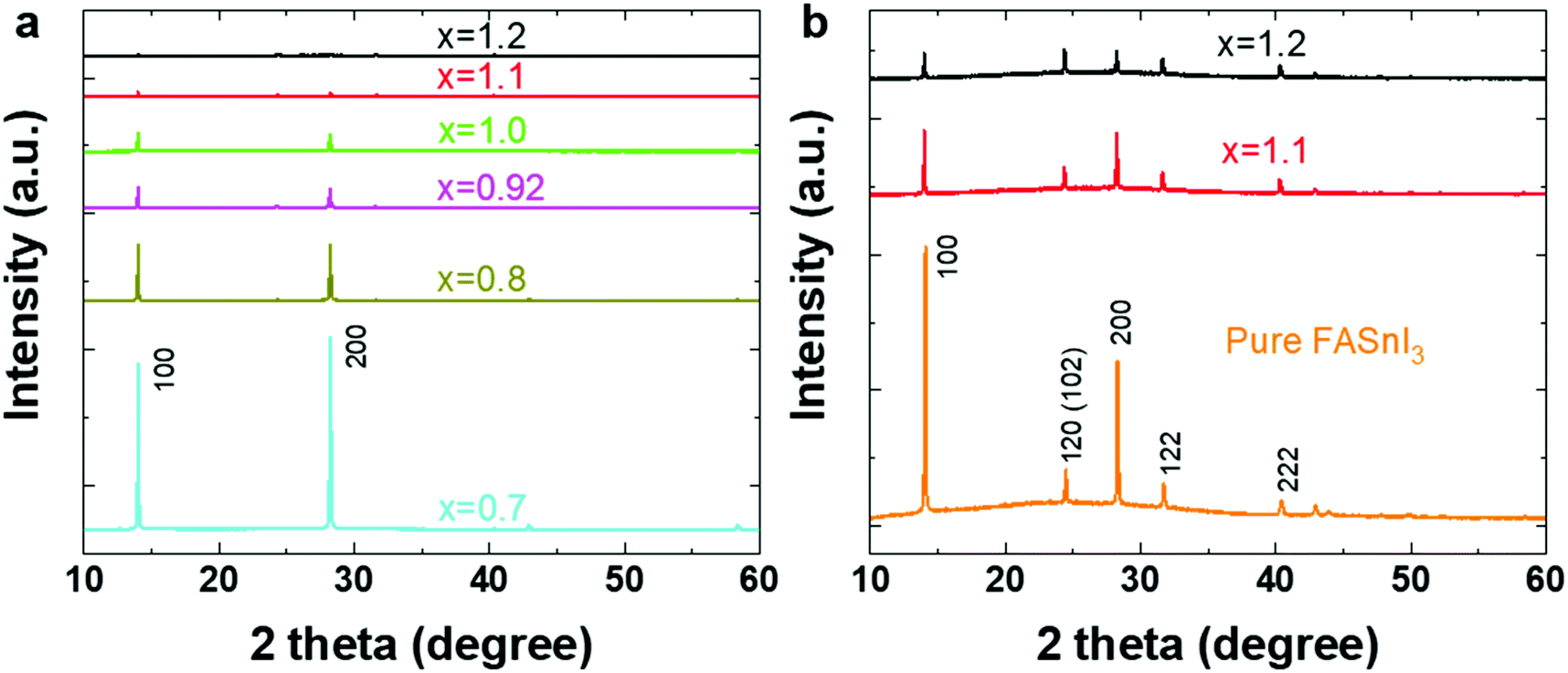 | ||
| Fig. 1 XRD patterns of PEA0.08FAxSnI3 films with (a) x ranging from 0.70 M to 1.20 M and (b) the 1.10 M and 1.20 M patterns compared to the one of pure FASnI3. | ||
We performed grazing incidence wide-angle X-ray scattering (GIWAXS) measurements to gain deeper insight into the effect of stoichiometry on the orientation of the 2D/3D films. Fig. 2 and S2† show GIWAXS images recorded at incident angles of 2° and 0.25° for the PEA0.08FAxSnI3 films. The X-ray penetrates through the entire film in the former case and only several tens of nanometers from the top part of the film in the latter case.18,19 Regardless of the penetration depth, the FA-deficient 2D/3D films (x ≤ 0.8) exhibit very sharp and intense Bragg spots for the (100) and (200) planes along the qz direction (out-of-plane), and very weak diffraction spots of these planes along the qr direction (in-plane). This shows that, similar to the situation of the reference 2D/3D film,18 the 3D tin perovskite phase is highly oriented with (h00) planes preferentially stacking in the out-of-plane direction throughout the entire film. The FA-deficient films detected at the two X-ray incident angles show pronounced diffraction patterns at qz ≈ 0.6 Å−1 and 0.78 Å−1, which are assigned to the (004) planes of the low-dimensional (2D) tin perovskite PEA2FASn2I7 (n = 2) and PEA2SnI4 (n = 1), respectively.28 Notably, they do not show these diffraction features along the qr direction, which indicates that the n = 1 and 2 phases exist throughout the entire film and lie preferentially with their inorganic layers parallel to the substrate. These FA-deficient films contain a remarkably higher amount of the 2D phases compared to the reference 2D/3D film which only has a very small amount of the 2D phase at the bottom of the film.18 The 2D/3D film containing a slight excess of FA (x = 1.00) also maintains the preferential orientation of the 3D phase, which shows diffraction patterns similar to that of the reference 2D/3D film.18,19 2D/3D films with a higher excess of FAI (x > 1) only exhibit broad diffraction arcs of the 3D phase, which is clear evidence for the randomly oriented 3D grains in these films. Moreover, these films do not show observable diffraction patterns of the 2D phases probably due to their extremely small quantity or absence (Fig. 2f and h). The variation in the amount of the 2D tin perovskite phase is caused by the competitive crystallization between the 3D and the 2D phase.28 Deficiency in FA facilitates the crystallization of 2D tin perovskite, while excess FA facilitates the crystallization of 3D tin perovskite. The quantity of the 2D tin perovskite determines the crystallinity and orientation of the 3D phase by changing its crystallization mechanism.28 The highly oriented 2D tin perovskite enables growth of the highly crystalline and oriented 3D phase in the 2D/3D tin perovskite films, while its absence causes randomly oriented 3D phases with poor crystallinity.18,19,28
 | ||
| Fig. 2 GIWAXS patterns of (a) the PEA0.08FA0.6SnI3, (b) PEA0.08FA0.7SnI3, (c) PEA0.08FA0.8SnI3, (d) PEA0.08FA1.0SnI3, (e) PEA0.08FA1.1SnI3 and (f) PEA0.08FA1.2SnI3 films. The images were recorded using an incident angle of 2°. Line-cut data of the PEA0.08FAxSnI3 (x = 0.6–1.1) films along (g) qr and (h) qz directions. | ||
Atomic force microscopy (AFM) images in Fig. 3 reveal the obvious difference in the morphology of the PEA0.08FAxSnI3 films due to the variation in the composition and crystallization behavior. Compared to the reference 2D/3D film, FA-deficient 2D/3D films (x ≤ 0.8) contain more flake-like grains due to more perfect orientation of the grains, and a significant number of large pinholes with the size larger than 500 nm at grain boundaries. In contrast, FA-excess 2D/3D films (x ≥ 1.1) do not show any large pin holes or flake-like features due to the random orientation of the grains in the absence of the 2D materials. These results are in line with the observation from GIWAXS measurements. Particularly, the FA-excess 2D/3D film (x = 1.2) appears to be non-textured due to its poor crystallinity. The scanning electron microscopy (SEM) images shown in Fig. S4† generally display features consistent with what is observed in the AFM images. A closer look at the FA-excess (x = 1.1) film reveals plenty of tiny pinholes (smaller than 50 nm) within grains, which are absent in the 2D/3D films with lower FA concentrations (x ≤ 1).
 | ||
| Fig. 3 AFM images of PEA0.08FAxSnI3 at a scan area of 5 μm × 5 μm. | ||
Photoluminescence (PL) spectroscopy is a useful tool to gain deeper insight into the effect of stoichiometry on the quality of the tin perovskite films.29,30Fig. 4a shows the steady-state PL spectra of PEA0.08FAxSnI3 films. The reference 2D/3D film exhibits an emission peak centered around 900 nm, which is due to the radiative recombination of the free holes and electrons. The FA-deficient films exhibit emission peaks at similar wavelengths to the reference 2D/3D film, while the FAI-excess films show blue-shifted emission peaks (Fig. S5†). These shifts in the photoluminescence are in agreement with the variation in absorbance spectra (Fig. S6†), which demonstrate an onset at approximately 900 nm for the reference sample and a blue-shifted onset for the FA-excess (x ≥ 1.1) film. Similar to the pure 3D films, the significant crystallographic disorder may cause severe p-doping in the extreme FA-excess films, which will be discussed later. The blue-shift in both absorbance and photoluminescence spectra of the FA-excess films is presumably associated with the Burstein–Moss effect due to the p-doping of the material,15,29 which shifts the edge of the valence band towards lower energy and enlarges the bandgap. Additionally, the broadening in the peak width of the FA-excess films is dominated by the disorder and the doping. The PL intensity (Fig. 4a) of the 2D/3D films decreases with increased FA concentration. Particularly, the FA-excess films show a much weaker PL intensity than the rest of the 2D/3D films. Therefore, we can state that FA-excess 2D/3D films show the highest non-radiative charge carrier recombination. Fig. 4b shows the decay dynamics of the photo-generated charge carriers in the PEA0.08FAxSnI3 films. Fitting the low intensity, the FA-excess film (x = 1.1) exhibits a short PL lifetime of 0.10 ns, while the reference 2D/3D film and slight FA-excess film exhibit PL lifetimes more than 20 times longer (2.27 ns and 3.50 ns). As further confirmed below, this is due to both the reduction of trap-assisted carrier recombination loss and the suppression of strong background doping for films of comparatively low FA-content. The charge carriers in the FA-deficient films have intermediate lifetimes. It is likely that 2D phases throughout the entire film and the excess SnI2 inhibit the diffusion of photo-generated carriers away from each other. Consequently, the recombination of the free holes and electrons increases, leading to strong emission but short charge carrier lifetime.
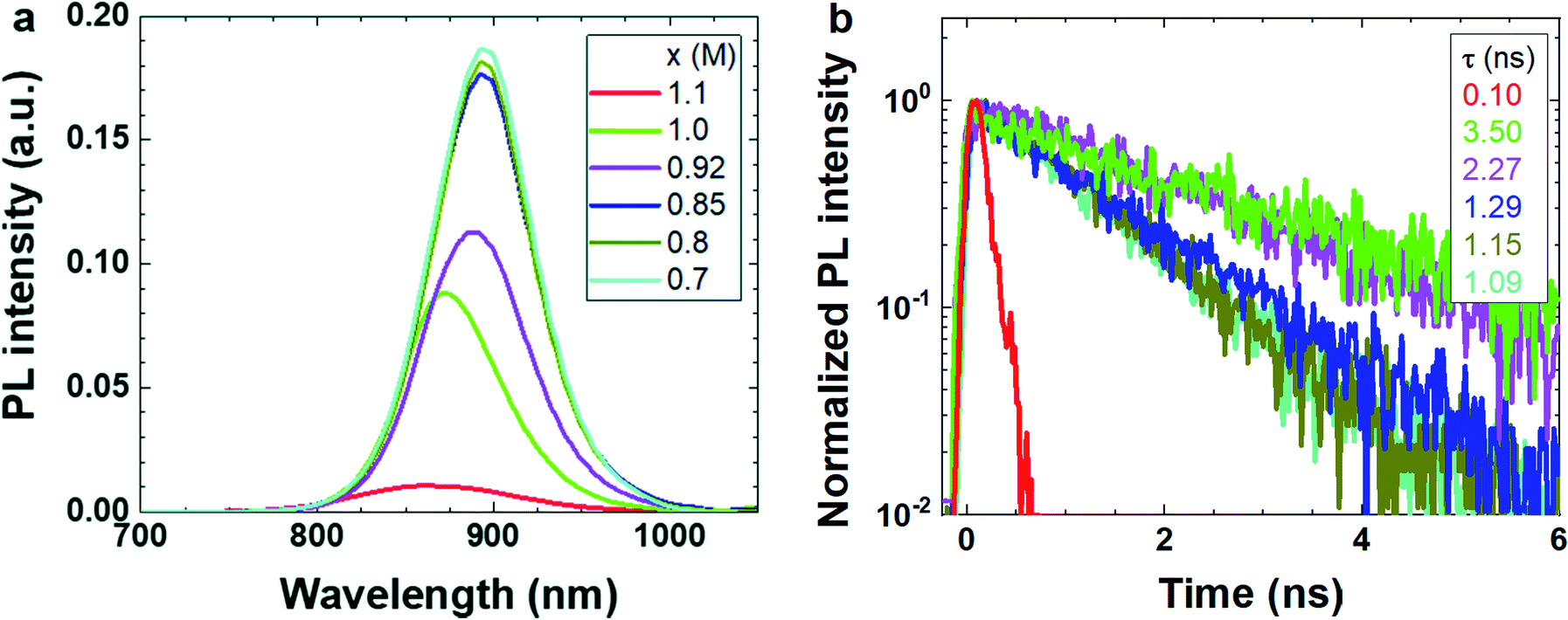 | ||
| Fig. 4 PL measurements of PEA0.08FAxSnI3 films. (a) Steady state and (b) time-resolved PL. The color scheme is the same in the two figures, lifetimes are reported in the legend of (b). | ||
To understand more about the intrinsic properties of PEA0.08FAxSnI3 films we performed conductivity measurements keeping the samples in the dark. Fig. 5a shows the current density–voltage (J–V) curves measured on a lateral device structure (see the Experimental details). As mentioned above, the electrical conductivity in tin based perovskite films is dominated by holes18,19 and tin vacancies are mainly responsible for the high degree of doping that is often encountered. Fig. 5b shows the conductivity values of the 2D/3D films. The FA-deficient films show electrical conductivity of the order of 10−4 S cm−1, which is similar to that of the reference 2D/3D film. Mott–Schottky analysis confirms that these films have a background hole density similar to that of the reference 2D/3D film (Fig. S7†). In contrast, the FA-excess films (x ≥ 1.1) are 20 times more conductive than the reference 2D/3D film due to much higher background hole density (Fig. S6†), indicating an increased number of tin vacancies.
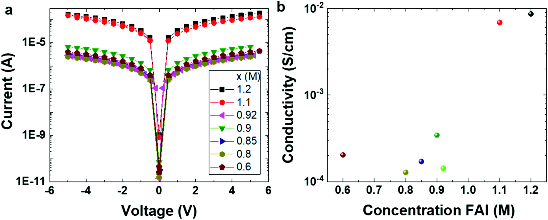 | ||
| Fig. 5 Conductivity measurements of PEA0.08FA(x)SnI3 films. (a) I–V characteristics under dark conditions, and (b) electrical conductivity calculated from the I–V curves in (a). | ||
With the knowledge on the properties of the tin perovskite films, we proceed further to investigate how the stoichiometry of the 2D/3D films influences the performance of solar cells. We fabricated devices using the architecture ITO/poly(3,4-ethylenedioxythiophene):polystyrene sulfonate (PEDOT:PSS)/PEA0.08FA(x)SnI3/C60/2,9-dimethyl-4,7-diphenyl-1,10-phenanthroline (BCP)/Al, following the fabrication method reported in our previous studies.18,19Fig. 6a shows the J–V curves of the solar cells tested under a light intensity of 100 mW cm−2 and AM 1.5G conditions. The reference HPSC exhibits an open circuit voltage (VOC) of 0.50 V, a short circuit current density (JSC) of 22.8 mA cm−2, and a fill factor (FF) of 0.69, which results in a PCE of about 8%, as shown in Table 1 and Fig. 6b. The devices based on slight FA-excess (x = 0.95 and 1.0) 2D/3D films deliver similar PCEs. These results can be explained by the fact that the PEA0.08FAxSnI3 (x in the range of 0.92 to 1) films have low trap-assisted charge carrier recombination. HPSCs based on 2D/3D films with a significant excess of FA exhibit a sharp drop in the VOC, JSC and FF, leading to a PCE lower than 1%. Such poor device performance is caused by the severe trap-assisted charge recombination and high shunt loss (Fig. 6c). These results show clearly that the concentration of FA should lie in the range of 0.92–1.0 M in order to obtain efficient 2D/3D based HPSCs. HPSCs based on FA-deficient films have slightly higher VOC than the best performing reference solar cell, but significantly lower JSC and FF. The statistics of the figures of merits for devices of different stoichiometries is shown in Fig. S8–S10.† As we discussed previously, the parallel oriented 2D phases and the presence of SnI2 hinder the charge transport and cause significant recombination of free electrons and holes, reducing JSC and FF in solar cells. The incident photon to electron conversion efficiency (IPCE) spectra (Fig. S11†) confirm the trend of the JSC.
 | ||
| Fig. 6 PEA0.08FAxSnI3 based devices. (a) J–V curves under AM 1.5G conditions, (b) PCE versus FA concentration and (c) J–V curves of the solar cells under dark conditions. Displayed results are coming from a batch of consistent samples. | ||
| X (M) | J sc (mA cm−2) | V oc (V) | FF | PCE (%) |
|---|---|---|---|---|
| 1.20 | 3.1 | 0.19 | 0.37 | 0.22 |
| 1.10 | 6.9 | 0.24 | 0.55 | 0.53 |
| 1.00 | 23.9 | 0.50 | 0.66 | 7.82 |
| 0.95 | 23.1 | 0.50 | 0.69 | 7.99 |
| 0.92 | 22.8 | 0.50 | 0.69 | 7.98 |
| 0.85 | 20.5 | 0.52 | 0.52 | 5.57 |
| 0.80 | 16.3 | 0.53 | 0.40 | 3.34 |
| 0.70 | 14.2 | 0.53 | 0.40 | 3.00 |
To gain deeper insight into the charge recombination in the solar cells, we tested their J–V curves under different light intensities. Fig. 7a shows the JSCvs. light intensity (I) plots. Fig. 7b shows the value of the slope (alpha) obtained by fitting the experimental data points from Fig. 7a assuming a power law dependence of the JSC on the light intensity (JSC ∝ Iα). The device based on the FA-deficient (x = 0.8) 2D/3D film shows an α value of about 0.81, confirming strong bimolecular recombination of electrons and holes in those devices.31 Again, this explains the origin of the low JSC and FF. The rest of the devices based on 2D/3D films with a higher FA concentration show α values of 0.88, due to reduced recombination of the free electrons and holes. Fig. 7c shows the VOCvs. semi-logarithmic light intensity plots, and Fig. 7d shows the ideality factor (n) values extracted from the slope of the former plots. Compared to the devices based on 2D/3D films with lower FA concentrations, the devices based on 2D/3D films with a significant excess of FA (x ≥ 1.1) exhibit much higher n values, verifying severe trap-assisted charge carrier recombination. Consequently, these devices suffer from low VOC and JSC.
 | ||
| Fig. 7 (a) JSC as a function of the light intensity, (b) the extracted values of α, (c) VOC as a function of the light intensity and (d) the extracted ideality factor n for the solar cells. | ||
We also tested the stability of the devices without any encapsulation exposing samples to ambient conditions for the indicated time and testing them back in the N2-filled glove box (see Fig. S12†). Generally, the FA-deficient devices (x ≤ 0.85) degrade quickly and lose their performance completely within 5 minutes of exposure to air even though they contain a remarkable amount of the low dimensional perovskite phase. The rest of the devices are much more stable compared to the FA-deficient devices, and maintain at least 60% of the initial performance after being exposed to air for 35 minutes. Such distinct degradation behavior for different FA concentrations is most probably associated with the film morphology. The severely FA-deficient 2D/3D film has a large quantity of pinholes, which allow moisture and oxygen to penetrate into the film more rapidly and therefore cause faster degradation in the device performance. Among the 2D/3D films with higher FA concentrations (x > 0.85), the device with significant FA-excess (x = 1.2) degrades faster probably due to the poor crystallinity of the film, which creates weak points prone to start degradation in the presence of oxygen and moisture. As a consequence of the enhanced crystallinity, the 2D/3D films with FA concentration ranging from 0.92 to 1.0 offer the most stable devices.
Conclusions
To summarize, we investigated the effects of the nominal stoichiometry of 2D/3D (PEA0.08FAxSnI3) tin perovskite films on their crystallization and solar cell performance. The reference 2D/3D film (x = 0.92) has a high crystallinity and preferential grain orientation, resulting in devices with low trap-assisted charge recombination and a PCE of 8.0%. 2D/3D tin perovskite films fabricated with a slightly increased FAI concentration (up to x = 1.00) exhibit a similar crystallization behavior to the reference samples, which in turn produces HPSCs with a PCE of about 8%. 2D/3D films with higher FAI concentration (x > 1.0) are less crystalline and display randomly oriented pure 3D phases. Conductivity measurements indicate a significantly higher trap density than that found for the reference film. Therefore, the fabricated solar cells suffer from severe trap-assisted charge recombination and exhibit a very low PCE of <1%. The 2D/3D films with significant deficiency in FAI (x ≤ 0.7) are composed of highly crystalline and oriented 3D grains, and a large quantity of 2D (n ≤ 2) phases oriented parallel to the substrate. Moreover, these films contain considerable amounts of SnI2. Consequently, the solar cells suffer from poor charge transport, displaying very low JSC and FF. Our results demonstrate that the stoichiometry of the tin perovskite film plays a critical role in the performance of the solar cells and in their stability. The chemical diversity of the 2D materials offers a great opportunity for obtaining efficient and stable 2D/3D tin based solar cells. So far, very limited bulky organic spacer cations have been investigated in the 2D/3D approach based tin perovskite solar cells. Designing new organic spacer cations with different functionalities for 2D materials combined with stoichiometry optimization has great potential to further improve the efficiency and stability of tin based perovskite solar cells.Experimental details
Materials
The PEDOT:PSS water dispersion (i.e. Clevios VP AI 4083) was purchased from Heraus. Tin iodide (SnI2) (99.99%), tin fluoride (SnF2) (>99%), buckminsterfullerene (C60) (>99.9%), bathocuproine (BCP) (99.99%), dimethyl sulfoxide (DMF) (99.8%) and N,N-dimethylformamide (DMSO) (99.8%) were bought from Sigma Aldrich. 2-Phenylethylammonium iodide (PEAI) (>98%) and formamidinium iodide (FAI) (>98%) were acquired from TCI EUROPE N.V. All materials were used as received.PEA0.08FAxSnI3 solutions were prepared in a nitrogen-filled glovebox. Here x indicates the molar concentration of FAI that has been added to the solution. To produce the PEA0.08FAxSnI3 precursor perovskite solution, (0.08 M) PEAI, (x M) FAI, (1 M) SnI2 and (0.1 M) SnF2 were dissolved in a mixture of DMF and DMSO (volume ratio of 4![[thin space (1/6-em)]](https://www.rsc.org/images/entities/char_2009.gif) :1). X is varied between 0.60 and 1.20 M. The solutions were stirred for a minimum of 6 hours before use.
:1). X is varied between 0.60 and 1.20 M. The solutions were stirred for a minimum of 6 hours before use.
SEM measurements
SEM images were recorded in vacuum on an FEI NovaNano SEM 650 with an acceleration voltage of 10 kV.XRD
XRD patterns of the perovskite films were recorded on a Bruker D8 Advance X-ray diffractometer with a Cu Kα source (λ = 1.54 Å) and a Lynxeye detector.GIWAXS measurements
Grazing incidence wide-angle X-ray scattering (GIWAXS) measurements were performed using a MINA X-ray scattering instrument built on a Cu rotating anode source (λ = 1.5413 Å) following the procedure reported in our previous work.18Steady-state and time-resolved PL measurements
Steady-state and time-resolved photoluminescence (PL) measurements were conducted by exciting the samples with the second harmonic (400 nm) of a mode-locked Ti:Sapphire femtosecond laser (Mira 900, Coherent). The repetition rate of the laser is 76 MHz; a pulse picker was inserted in the optical path to decrease the repetition rate of the laser pulses. The excitation beam was focused with a 150 mm focal length lens, and the emission was collected and coupled into a spectrometer with a 50 lines per mm grating. The steady-state PL was recorded with an Image EM CCD camera from Hamamatsu (Hamamatsu, Japan). Time-resolved PL was measured with a Hamamatsu streak camera working in single sweep mode.Electrical conductivity and C–V measurements
For the electrical conductivity measurements, parallel line-shape Au electrodes with a width (w) of 13 mm and a channel length (L) of 200 μm were deposited on cleaned glass substrates as bottom contacts. Different perovskite films were spin-coated on the patterned glass following the same procedure used for photovoltaic device fabrication. Voltage-sourced two-point conductivity measurements were conducted using a probe station in a N2 glovebox. The electrical conductivity (σ) was calculated according to the formula σ = (J/V) × L/(w × d), where d is the thickness of the perovskite films. The capacitance–voltage (C–V) measurements were conducted under dark conditions at a frequency of 10 KHz with an AC drive voltage of 20 mV and DC bias in the range of −0.6 to 0.6 V on a Solartron 1260 impedance gain-phase analyzer.UV-Vis measurements
UV-Vis spectra of the perovskite films were recorded on a UV-Vis-NIR spectrometer Shimadzu UV-3600.Device fabrication
ITO glass substrates were cleaned using an ultrasonic bath in soap water and rinsed sequentially with deionized water, acetone and isopropyl alcohol. A PEDOT:PSS layer was then spin-coated onto the ITO substrates at 4000 rpm for 60 s and dried at 140 °C for 20 min. The coated substrates were then transferred to a nitrogen-filled glovebox. The tin based perovskite films were spin-coated from their precursor solutions at 4000 rpm for 60 s. Toluene was used as the anti-solvent during the spin-coating process. These films were then annealed at 70 °C for 20 min. Next, 30 nm C60, 6 nm BCP and 100 nm Al layers were sequentially evaporated on top of the perovskite film under a vacuum of <10−6 mbar. The J–V curves of the perovskite solar cells were measured at 295 K using a Keithley 2400 source meter under simulated AM 1.5G solar illumination using a Steuernagel Solar constant 1200 metal halide lamp in a nitrogen-filled glovebox. The light intensity was calibrated to be 100 mW cm−2 by using a Si reference cell and correcting the spectral mismatch. A shadow mask (0.04 cm2) was used during the J–V measurements.Conflicts of interest
There are no conflicts of interest to declare.Acknowledgements
We thank Arjen Kamp and Teo Zaharia for their kind technical support in the laboratory. S. K. acknowledges the Deutsche Forschungsgemeinschaft (DFG) for a postdoctoral research fellowship (grant number 408012143). This work was financed through the Materials for Sustainability (Mat4Sus) programme (739.017.005) of the Netherlands Organisation for Scientific Research (NWO).References
- M. A. Green, A. Ho-Baillie and H. J. Snaith, Nat. Photonics, 2014, 8, 506 CrossRef CAS
.
- J. Even, L. Pedesseau, J.-M. Jancu and C. Katan, J. Phys. Chem. Lett., 2013, 4, 2999–3005 CrossRef CAS
- G. Xing, N. Mathews, S. Sun, S. S. Lim, Y. M. Lam, M. Gratzel, S. Mhaisalkar and T. C. Sum, Science, 2013, 342, 344–347 CrossRef CAS PubMed
- A. Kojima, K. Teshima, Y. Shirai and T. Miyasaka, J. Am. Chem. Soc., 2009, 131, 6050–6051 CrossRef CAS PubMed
- S. Shao, H. Duim, Q. Wang, B. Xu, J. Dong, S. Adjokatse, G. R. Blake, L. Protesescu, G. Portale, J. Hou, M. Saba and M. A. Loi, ACS Energy Lett., 2019, 5, 39–46 CrossRef
- M. He, D. Zheng, M. Wang, C. Lin and Z. Lin, J. Mater. Chem. A, 2014, 2, 5994–6003 RSC
- W. Ning and F. Gao, Adv. Mater., 2019, 31, 1900326 CrossRef PubMed
- M. Saliba, T. Matsui, K. Domanski, J.-Y. Seo, A. Ummadisingu, S. M. Zakeeruddin, J.-P. Correa-Baena, W. R. Tress, A. Abate, A. Hagfeldt and M. Grätzel, Science, 2016, 354, 206–209 CrossRef CAS PubMed
- H. Yu, F. Wang, F. Xie, W. Li, J. Chen and N. Zhao, Adv. Funct. Mater., 2014, 24, 7102–7108 CAS
- F. Wan, L. Ke, Y. Yuan and L. Ding, Sci. Bull., 2020, 66, 417–420 CrossRef
- A. Filippetti and A. Mattoni, Phys. Rev. B, 2014, 89, 125203 CrossRef
- A. H. Slavney, L. Leppert, D. Bartesaghi, A. Gold-Parker, M. F. Toney, T. J. Savenije, J. B. Neaton and H. I. Karunadasa, J. Am. Chem. Soc., 2017, 139, 5015–5018 CrossRef CAS PubMed
- I. Chung, B. Lee, J. He, R. P. H. Chang and M. G. Kanatzidis, Nature, 2012, 485, 486–489 CrossRef CAS PubMed
- J. Jiang, C. K. Onwudinanti, R. A. Hatton, P. A. Bobbert and S. Tao, J. Phys. Chem. C Nanomater. Interfaces, 2018, 122, 17660–17667 CrossRef CAS PubMed
- H.-H. Fang, S. Adjokatse, S. Shao, J. Even and M. A. Loi, Nat. Commun., 2018, 9, 243 CrossRef PubMed
- S. Kahmann and M. A. Loi, J. Mater. Chem. C, 2019, 7, 2471–2486 RSC
- W. Ke, C. C. Stoumpos, I. Spanopoulos, L. Mao, M. Chen, M. R. Wasielewski and M. G. Kanatzidis, J. Am. Chem. Soc., 2017, 139, 14800–14806 CrossRef CAS PubMed
- S. Shao, J. Liu, G. Portale, H.-H. Fang, G. R. Blake, G. H. ten Brink, L. Jan Anton Koster and M. A. Loi, Adv. Energy Mater., 2018, 8, 1702019 CrossRef
- S. Shao, J. Dong, H. Duim, G. H. ten Brink, G. R. Blake, G. Portale and M. A. Loi, Nano Energy, 2019, 60, 810–816 CrossRef CAS
- D. Meggiolaro, D. Ricciarelli, A. A. Alasmari, F. A. S. Alasmary and F. De Angelis, J. Phys. Chem. Lett., 2020, 11, 3546–3556 CrossRef CAS PubMed
- Y. Wang, J. Tu, T. Li, C. Tao, X. Deng and Z. Li, J. Mater. Chem. A, 2019, 7, 7683–7690 RSC
- C. Roldán-Carmona, P. Gratia, I. Zimmermann, G. Grancini, P. Gao, M. Graetzel and M. K. Nazeeruddin, Energy Environ. Sci., 2015, 8, 3550–3556 RSC
- Q. Ma, S. Huang, S. Chen, M. Zhang, C. F. J. Lau, M. N. Lockrey, H. K. Mulmudi, Y. Shan, J. Yao, J. Zheng, X. Deng, K. Catchpole, M. A. Green and A. W. Y. Ho-Baillie, J. Phys. Chem. C, 2017, 121, 19642–19649 CrossRef CAS
- M. Yang, D. H. Kim, Y. Yu, Z. Li, O. G. Reid, Z. Song, D. Zhao, C. Wang, L. Li, Y. Meng, T. Guo, Y. Yan and K. Zhu, Mater. Today Energy, 2018, 7, 232–238 CrossRef
- H. Duim, S. Adjokatse, S. Kahmann, G. H. ten Brink and M. A. Loi, Adv. Funct. Mater., 2020, 30, 1907505 CrossRef CAS
- K. P. Marshall, R. I. Walton and R. A. Hatton, J. Mater. Chem. A, 2015, 3, 11631–11640 RSC
- T.-B. Song, T. Yokoyama, S. Aramaki and M. G. Kanatzidis, ACS Energy Lett., 2017, 2, 897–903 CrossRef CAS
- J. Dong, S. Shao, S. Kahmann, A. J. Rommens, D. Hermida-Merino, G. H. ten Brink, M. A. Loi and G. Portale, Adv. Funct. Mater., 2020, 30, 2001294 CrossRef CAS
- S. Kahmann, O. Nazarenko, S. Shao, O. Hordiichuk, M. Kepenekian, J. Even, M. V. Kovalenko, G. R. Blake and M. A. Loi, ACS Energy Lett., 2020, 5, 2512–2519 CrossRef CAS
- S. Kahmann, S. Shao and M. A. Loi, Adv. Funct. Mater., 2019, 29, 1902963 CrossRef
- J. Liu, X. Li, S. Zhang, X. Ren, J. Cheng, L. Zhu, D. Zhang, L. Huo, J. Hou and W. C. H. Choy, Adv. Mater. Interfaces, 2015, 2, 1500324 CrossRef
Footnotes |
| † Electronic supplementary information (ESI) available. See DOI: 10.1039/d0ta10277f |
| ‡ Dr S. Shao and M. Nijenhuis contributed equally to this work. |
| This journal is © The Royal Society of Chemistry 2021 |