
 Open Access Article
 This Open Access Article is licensed under a Creative Commons Attribution-Non Commercial 3.0 Unported Licence
Recent trends in graphene supercapacitors: from large area to microsupercapacitors
Andres
Velasco
ab,
Yu Kyoung
Ryu
a,
Alberto
Boscá
ab,
Antonio
Ladrón-de-Guevara
c,
Elijah
Hunt
a,
Jinghan
Zuo
d,
Jorge
Pedrós
ab,
Fernando
Calle
ab and
Javier
Martinez
 *ae
*ae
aInstituto de Sistemas Optoelectrónicos y Microtecnología, Universidad Politécnica de Madrid, Av. Complutense 30, Madrid 28040, Spain. E-mail: javier.martinez@upm.es
bDepartamento de Ingeniería Electrónica, E.T.S.I de Telecomunicación, Universidad Politécnica de Madrid, Av. Complutense 30, Madrid 28040, Spain
cHajim School of Engineering and Applied Physics, University of Rochester, Rochester, NY 14627, USA
dSchool of Materials Science and Engineering, Beihang University, Beijing 100191, China
eDepartamento de Ciencia de Materiales, E.T.S.I de Caminos, Canales y Puertos, Universidad Politécnica de Madrid, C/ Profesor Aranguren s/n, Madrid 28040, Spain
First published on 29th January 2021
Abstract
Supercapacitors are being increasingly used as energy storage systems. Graphene, with its huge specific surface area, superior mechanical flexibility and outstanding electrical properties, constitutes an ideal candidate for the next generation of wearable and portable devices with enhanced performance. Since Stoller described the first graphene supercapacitor in 2008, significant developments have been made during this last decade in the development of new graphene-based electrodes. In this way, the specific capacitance has been improved from 135 to 2585 F g−1 and the cyclability has been enhanced from a capacitance retention of just over 80% after 1000 cycles to almost 100% after 20![[thin space (1/6-em)]](https://www.rsc.org/images/entities/char_2009.gif) 000 cycles. This review describes how 3-dimensional porous graphene electrodes have been improved recently, from using large area processing techniques to microsupercapacitors. Specifically, (a) the use of graphene foam to obtain large area electrodes, (b) the development of the direct laser writing technique for fast, one-step, and low-cost production of graphene-based supercapacitors, (c) their miniaturization in the form of integrated microsupercapacitors and (d) their functionalization with different pseudocapacitive and electric double-layer capacitor materials to obtain higher capacitance values will be the topics discussed in this perspective.
000 cycles. This review describes how 3-dimensional porous graphene electrodes have been improved recently, from using large area processing techniques to microsupercapacitors. Specifically, (a) the use of graphene foam to obtain large area electrodes, (b) the development of the direct laser writing technique for fast, one-step, and low-cost production of graphene-based supercapacitors, (c) their miniaturization in the form of integrated microsupercapacitors and (d) their functionalization with different pseudocapacitive and electric double-layer capacitor materials to obtain higher capacitance values will be the topics discussed in this perspective.
1 Introduction
Supercapacitors are energy storage devices, which, in contrast to batteries, show a high power performance, with short charge and discharge times and almost no degradation over long-term cycling.1–4 However, these devices cannot match the high energy density achievable by batteries.5 In order to get both high power and high energy density at the same time, the coupling of supercapacitors and batteries as hybrid energy storage systems has been actively explored during the last few years for new applications such as electric vehicles.6–8 The development of the next generation of supercapacitors that will be components in wearable electronics for self-charging devices, especially in the field of the Internet of Things (IoT), is also one of the fundamental challenges that are currently taken care of.9–13Supercapacitors can be divided in two types according to the charge storage mechanism: electric double-layer capacitors (EDLCs) and pseudocapacitors, plus their hybrid combinations. EDLCs store energy electrostatically as image charges to the ions of the electrolyte, by an electric double layer surrounding the electrode–electrolyte interface, as modeled by Gouy–Chapman–Stern.14 This physical process, through non-faradaic charge transfer, is reversible at very high rates and can reach very high powers, while the energy density is small, limited by the 0.18 electrons that every carbon atom can store.15Fig. 1a shows a simplified scheme of an EDLC. Pseudocapacitors, on the other hand, make use of fast and reversible surface redox reactions of active materials in electrodes, such as conductive polymers or metal oxides, to increase the amount of charge that can be stored, at the expense of reducing the power and cyclability of the device16,17 (scheme represented in Fig. 1b). The main components of a supercapacitor are the electrodes, the corresponding current collectors, a separator between them and an electrolyte, as represented in the scheme shown in Fig. 1c. The electrolyte can be a liquid solvent or a solid-state or quasi-solid-state material18,19. When the electrochemical performance of a material as a potential electrode is of interest, rather than the performance of the whole supercapacitor, the measurements are taken in a three-electrode configuration, as depicted in Fig. 1d. Here, the components are a reference electrode, which is used to be able to locate electrochemical features at the right potentials, a counter electrode, and the electrode under study as the working electrode, all immersed into the electrolyte. However, to determine the charge transfer performance of the full device, a two-electrode measurement is needed, using only a working and a counter electrode that correspond, respectively, to the cathode and anode of the supercapacitor20. In order to compare the performance of supercapacitors built with different carbon materials and pseudocapacitive elements, their designs and standard figures-of-merit should match.21 The main relevant factor regarding supercapacitors is the capacitance, which is the amount of charge that the device can store in relation to the total change in its electric potential. However, the capacitance, in farads, is a meaningless number if it is not normalized by the total mass of the electrodes, or by the volume or area the device occupies. For regular supercapacitors, gravimetric or specific values are considered the most important figures-of-merit, normalized by the mass of the active material, in F g−1. Other relevant factors, also reported in this normalized format, are the specific energy density, in W h kg−1, and the specific power density, in W kg−1, of the device. For the specific case of thin film electrodes and microsupercapacitors, gravimetric values are not as relevant as the mass of the electrodes is typically negligible; therefore these metrics are typically given as areal or volumetric values.22,23
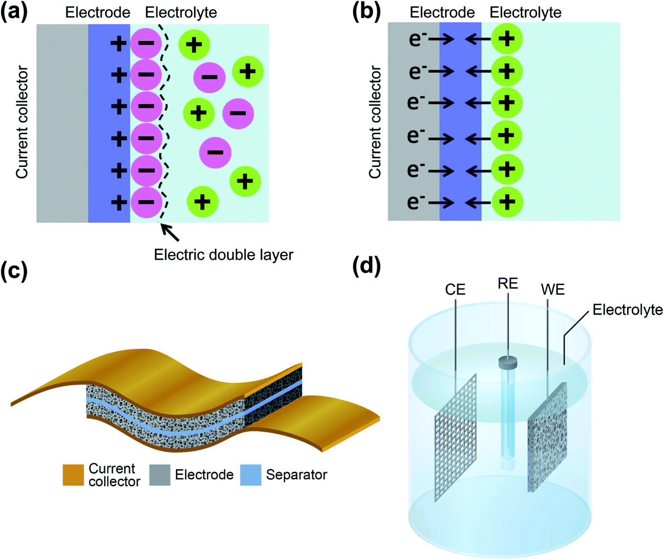 | ||
| Fig. 1 Scheme of (a) an electric double-layer capacitor and (b) a pseudocapacitor. (c) Schematic drawing of an assembled supercapacitor with a sandwich structure showing current collectors, electrodes and the separator, as used in two-electrode measurements. (d) Schematic drawing of a three-electrode measurement set-up showing a reference electrode, a Pt mesh as the counter electrode and one supercapacitor electrode as the working electrode, all immersed in the electrolyte. | ||
Among the several electrode candidates for optimal supercapacitors, graphene has attracted increasing attention due to its striking mechanical, optical and electrical properties and several effective strategies to synthesize it have been developed and optimized, since its discovery in 2004.24 Specifically in the energy storage field, its high potential as a next generation supercapacitor electrode is due to three main reasons:
(a) Graphene has the highest known surface area of 2630 m2 g−1 (ref. 25) and a very low theoretical density of 2.28 g cm−3.26 With these characteristics, the material has simultaneously a high packing density capability and a very large specific surface area for the interaction of electrons and ions.
(b) It presents an excellent electrical conductivity, with very high mobilities that can reach 200000 cm2 V−1 s−1 at room temperature,27–29 which enables the fast transfer of electrons and ions through the different device interfaces (electrode/electrolyte and electrode/collector). Also because of the high electrical conductivity, graphene can act simultaneously as an active material and current collector, avoiding the use of extra materials such as binders and additives.
(c) Graphene also shows high mechanical strength, with a Young's modulus of 1 TPa and a demonstrated reversible strain up to 25%,30 which makes it suitable for its application in flexible and printable electronics, maintaining a high capacitance retention.
Graphene in four dimensional structures (0D to 3D) has been explored as a component for supercapacitors, since the size and morphology of a material have influence on its physical and chemical properties.31 Among them, 3D graphene-based structures are the most studied because they have an intrinsic interconnected pore structure that provides a large surface area for interaction with ions and electrons and allows a high mass loading of pseudocapacitive materials, characteristics that are fundamental for highly performing supercapacitors. Consequently, three-dimensional graphene structures32–34 constitute the focus of the present review, with a special emphasis on the most promising techniques for making 3D graphene electrodes in terms of the achievable surface area, capacity, cyclability, cost-effectiveness and their integration in novel functional applications: (a) graphene foam (GF), (b) graphene materials fabricated by the direct laser writing method (DLW) and (c) graphene as an electrode in microsupercapacitors (MSCs).
(a) Within the family of 3D sponge graphene structures,35 graphene foam (GF) obtained from the reduction of graphene oxide (rGO) by chemical methods36–39 and by chemical vapor deposition (CVD)40–43 represents the focus in Section 2.1. The improvement of its energy density and operating voltage window as a supercapacitor by filling it with other carbon-based materials such as carbon nanotubes (CNTs)44–46 or pseudocapacitive materials such as metal oxides,47–49 metal hydroxides50–53 and conductive polymers54–57 is also discussed within the section.
(b) The direct laser writing method (DLW) applied to produce materials such as laser reduced graphene oxide (LrGO) or laser induced graphene (LIG) was developed by El-Kady et al.58,59 and constitutes the focus of Section 2.2. The optimization of the fabrication process will lead to the one-step, low-cost and fast production of porous graphene-based supercapacitors. Moreover, the DLW technique bridges the gap between large area electrodes and microelectrodes,60 making it a very versatile technology worth developing further. As in the case of graphene foam, the performance improvement of supercapacitors based on LrGO or LIG by the addition of pseudocapacitive or EDLC materials61,62 is discussed within the section.
(c) Finally, in Section 2.3, microsupercapacitors (MSCs) based on 3D graphene are discussed, since they are fundamental for enabling new applications that are useful in many industries, from complementing batteries for better power management to their integration with energy harvesters in self-powering modules. MSCs can be fabricated on flexible substrates and show better power performance and cyclability than batteries, extending the lifetime of the system and making them virtually maintenance-free, being the last requirement fundamental for medical applications. Wireless sensors for the Internet of Things, wearable electronics and implantable medical devices are examples of fields where microsupercapacitors play a key role.22,63
In Section 3, the regions in the Ragone plot show the evolution and future tendencies of the graphene electrodes described in Section 2.
2 Graphene electrodes
2.1 Electrodes fabricated with graphene foam
As mentioned in the Introduction, due to its large surface area and high conductivity, graphene was used for the first time as an electrode for supercapacitors by Ruoff's group.25 Since then, to reduce the agglomeration of graphene sheets to maximize the accessible surface area and the creation of large area supercapacitors constitute strategies that are continuously sought. One of the successful approaches up to now has been the use of graphene foam (GF) synthesized by CVD.64 By means of CVD processing, graphene can be grown on copper or nickel foam, and also to a lesser extent on other catalytic metal foam. High quality, single layer graphene can be grown on copper foam, but this thin structure collapses easily when removing the metal support. By using nickel foam, multilayer graphene is grown and by removing carefully the metal template, a self-standing 3D graphene foam structure is formed. This graphene foam allows building flexible, lightweight electrodes with an area of several cm2 and heights in the order of millimeters with a high conductivity. The interconnected network of macroscopic, open pores allows a rapid diffusion of the electrolyte ions. Nickel foam can also be used as a template to form rGO foam from chemical synthesis.65,66 The disadvantage of this type of graphene foam is that the typical diameter of its pores, in the range of 100 to 500 microns, is quite large. This size of the pores is determined by the diameter of the pores of the initial metal foam. A solution is using graphene foam as a conductive scaffold for the deposition or filling of pseudocapacitive and/or other carbon elements to create highly efficient composites. The graphene foam provides outstanding conductivity and structural stability. The added material of the composite, in intimate contact with graphene, creates faster and shorter transfer paths of electrons and ions for achieving a higher power density. The common composite partners of graphene foam have been metal oxides,67–71 conductive polymers57,72–76 or metal hydroxides53,77,78 mainly because both types of materials are low-cost and already well known in the field of pseudocapacitors. Among the metal oxides, several bimetallic oxides have demonstrated higher electrical conductivity and redox activity than monometallic oxides such as ZnO, NiO or Co3O4. Therefore, bimetallic oxides have been used for filling the graphene foam.79–83 Yu et al.79 deposited NiCo2O4 nanoneedles on graphene foam, achieving a specific capacity of 1588 F g−1 at 1 A g−1. Sun et al.80 used NiCo2O4 nanoparticles as pseudocapacitive materials and achieved a specific capacity of 2300 F g−1 at 1 A g−1, with a capacitance retention of up to 92% after 4000 cycles at 10 A g−1. Conductive polymers provide greater electrical conductivity and structural stability than some metal oxides. Pedrós et al.57 electrodeposited a sponge of polyaniline (PANI) nanofibers, 100 nm thick and several microns long, that filled partially the GF pores. They demonstrated that with only an 11% coverage of the pores, it is possible to obtain high gravimetric and volumetric capacitances of 1474 F g−1 and 86 F cm−3 at 0.47 A g−1, respectively. In this case the capacitance retention was up to 83% after 15000 cycles. In some studies, ternary composites have been explored as well,84,85 where graphene foam is paired with two different pseudocapacitive elements or a pseudocapacitive element plus an electric double-layer one. For example, Tseng et al.85 added activated carbon (electric double-layer material) and MnO2 (pseudocapacitive material) to graphene foam to form a composite.
One of the strategies for increasing the power density and the operating potential window of graphene foam-based electrodes, while maintaining the highest energy density possible, consists in the fabrication of asymmetric supercapacitors.77,86–90 In the work of Zhang et al.,86 an asymmetric supercapacitor composed of graphene foam/MnO2 and graphene foam/polypyrrole electrodes demonstrated a stable operating voltage window of 1.8 V and a capacitance retention of around 90% after 10000 cycles. In another remarkable study, Saeed et al.90 fabricated an asymmetric supercapacitor consisting of a novel graphene foam/CNTs/MoO3 ternary composite as the positive electrode and a graphene foam/CNT composite as the negative electrode. The scheme of the fabrication process is shown in Fig. 2a. This asymmetric cell demonstrated an outstanding capacitance retention of 94% after 10000 cycles and an operating voltage window of 1.6 V. The graphene foam/CNTs/MoO3 electrode exhibited a high specific capacitance of 1503 F g−1 at 1 A g−1, see Fig. 2b, as well as an exceptional capacitance retention of 96.5% after 10000 cycles.
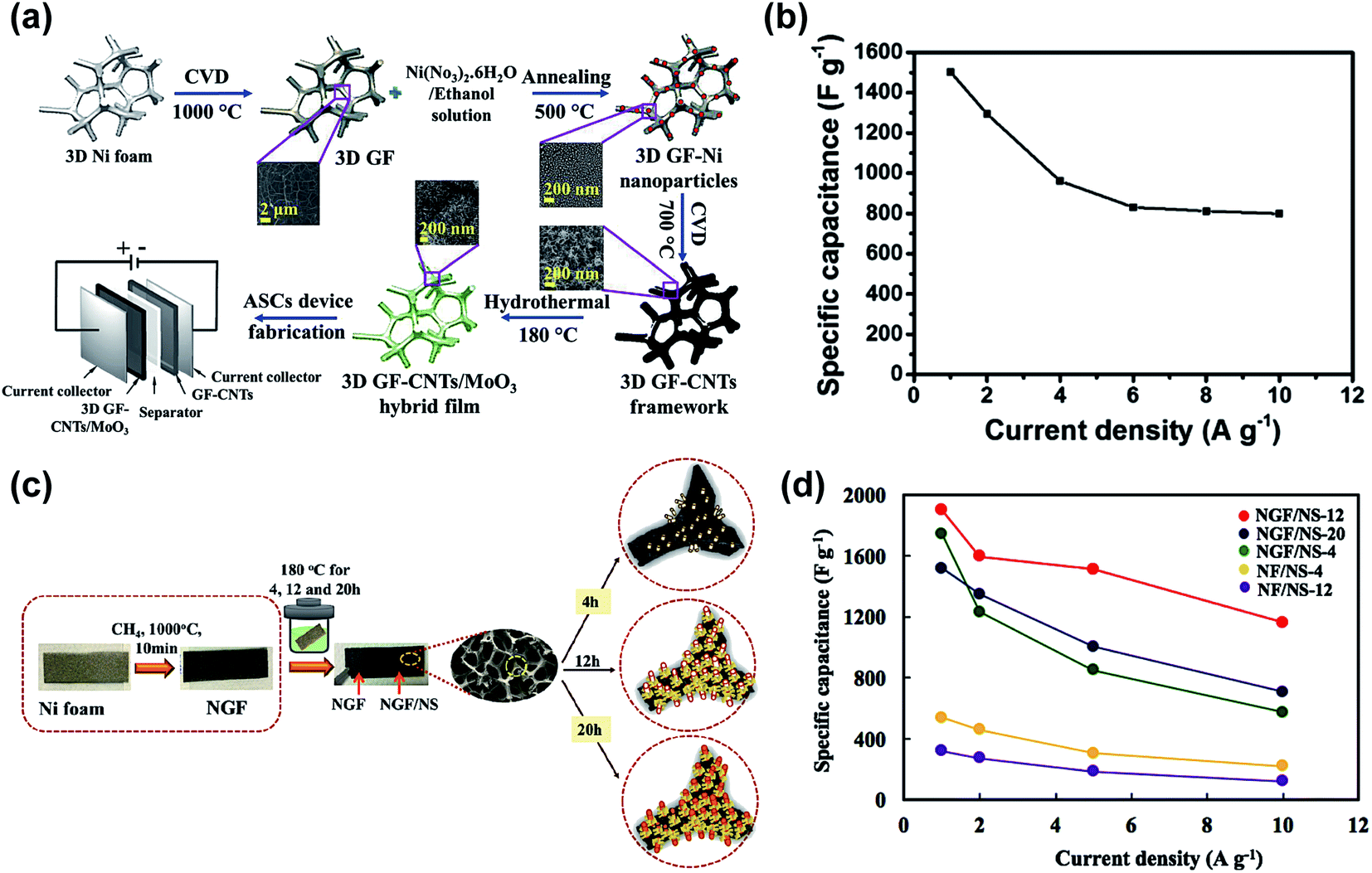 | ||
| Fig. 2 Different examples of graphene foam (GF) supercapacitors: (a) schematic diagram illustrating all steps involved in the synthesis of 3D GF/CNTs/MoO3 hybrid film-based electrode and the asymmetric supercapacitor device and (b) specific capacitance vs. current density obtained with this supercapacitor. (a) and (b) are reproduced with permission from ref. 90. Copyright 2018 Elsevier B.V. (c) Schematic diagram of the fabrication process of the Ni-GF/Ni3S2 nanocomposite electrode and (d) specific capacitances of different electrode materials plotted as a function of current density. (c) and (d) are reproduced with permission from ref. 96. Copyright 2018 Elsevier B.V. | ||
In this section, we have observed that the fabrication of graphene foam/pseudocapacitive material-based composites is the strategy of choice to optimize the performance of graphene as an electrode for supercapacitors, but generally at the expense of a cycling stability reduction. Therefore, new materials such transition metal sulfides are investigated as potential pseudocapacitive elements.91–100 As represented in the scheme shown in Fig. 2c, Kamali-Heidari et al.96 grew hierarchically Ni3S2 nanorods on CVD graphene foam, to achieve a specific capacitance of 1900 F g−1 at a current density of 1 A g−1 (Fig. 2d) and a capacitance retention of 96% after 2000 cycles. Kang et al.97 grew NiCo2S4 nanowires on CVD graphene foam, which provided a specific capacitance of 1454 F g−1 at 1.3 A g−1 and a capacitance retention of 96% after 3000 cycles at 13 A g−1. These recent results show that under optimization, new material combinations could provide higher electrical conductivity and structural stability than metal oxides and conductive polymers.
Another direction to improve the capacitance of graphene foam based supercapacitors is the maximization of the electrochemically available surface area and the minimization of the collapse or restacking of the graphene foam pores. This can be achieved by optimizing the metallic foam used as the template. As we explained at the beginning of this section, the diameter of the pores from typical commercial Cu or Ni foam lies in the range of 100 to 500 microns. The density and the diameter of Cu or Ni foam can be tuned by adjusting the catalyst particle size and the growth temperature. In this way, Drieschner et al.101 fabricated Cu and Ni foam with smaller pores that were produced by CVD, and graphene foam with pore sizes in the range of 0.5 to 30 microns, which presented an electrochemically available surface area 10000 times larger than that of the graphene foam fabricated by using commercial metal templates. These small pore GFs also presented a higher mechanical stability after the removal of the template by etching and a capacitance retention of almost 100% after 10000 cycles at 4 mA cm−3. Another group achieved GF with 1 μm size pores by CVD using sintered Ni nanoparticles as template.102 Recently, a graphene foam composed mainly of mono- and bi-layers was achieved by designing a Ni–Cu foam alloy.103 Another group, starting from commercial Ni foam, created a Ni–Cu foam alloy where they further synthesized Cu–Ni microbranches of 2–5 microns in diameter and 20–30 microns in length. These highly dense microbranches reduced the percentage of empty porous space in the commercial Ni foam by up to 63%.104 3D-printed porous silica templates designed with different pore/void sizes and complex architectures were used to obtain GF by CVD with a large surface area, 994.2 m2 g−1, and good mechanical properties.105
Finally, graphene foam and its composites have been proven to have high potential in advanced applications. For example, GF synthesized by CVD and coated with polypyrrole (PPy) has shown outstanding flexibility (180°) and stretchability (up to 50% strain).74 These properties were used to fabricate a device with a pressure-temperature dual sensor connected to a supercapacitor, where the common active material of both components was a PDMS/PPy/GF/composite.106 These devices could be bent up to 5% and exhibit almost no performance degradation over 10000 cycling under load pressure, which shows their suitability for stretchable and wearable electronics. This integrated device is shown in Fig. 3.
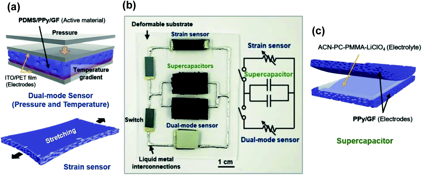 | ||
| Fig. 3 (a) Schematic drawing of a pressure/temperature sensor and a strain sensor based on polypyrrole/graphene-foam material. (b) Picture showing the electric circuit connecting these elements with two supercapacitors using liquid metal interconnects. (c) Schematic drawing of the PPy/GF sandwich supercapacitor. Reproduced with permission of ref. 106. Copyright 2018 Wiley-VCH Verlag GmbH & Co. KGaA, Weinheim. | ||
To conclude this section, we provide Table 1, where we have summarized the graphene foam based electrodes (with their corresponding references) that we have found to present the best performance in terms of specific capacitance and cyclability during the last 5 years. We have arranged them in chronological order, to track the trends in performance and chosen composite materials over time.
| Graphene foam fabrication method | Active material | Specific capacitance (F g−1) | Retention (%) after a number of cycles | Year | Ref. |
|---|---|---|---|---|---|
| CVD | Ni(OH)2 nanoflakes | 900 at 1 A g−1 | 98% at 2 A g−1 after 3000 | 2015 | 53 |
| rGO | NiCo2S4 nanoparticles | 1526 at 1 A g−1 | 83% at 10 A g−1 after 2000 | 2015 | 98 |
| CVD | NiCo2O4 flowers | 1402 at 1 A g−1 | 76.6% at 5 A g−1 after 5000 | 2015 | 81 |
| CVD | NiCo2O4 nanoneedles | 1588 at 1 A g−1 | 85.7% at 10 A g−1 after 2000 | 2015 | 79 |
| CVD | PANI nanofibers | 1474 at 0.47 A g−1 | 83% at 28 mA cm−2 after 15000 |
2016 | 57 |
| rGO | Ni–Co layered double hydroxide nanowires | 1041 at 2.5 mA cm-2 | 95% at 12.5 mA cm−2 after 2000 | 2016 | 77 |
| rGO | NiCo2O4 nanoparticles | 2300 at 1 A g−1 | 92% at 10 A g−1 after 4000 | 2016 | 80 |
| CVD | Co(OH)2 nanoflakes | 1636 at 0.5 A g−1 | 75% at 20 mV s−1 after 1000 | 2017 | 78 |
| CVD | V2O5 flowers | 1235 at 2 A g−1 | 92% at 4 A g−1 after 5000 | 2017 | 70 |
| CVD | Mn3.63Co5.37S8 nanohoneycombs | 1938 at 5 A g−1 | 82% at 50 A g−1 after 4000 | 2017 | 92 |
| RGO | H–CoMoO4 nanoplates | 1472 at 1 mA cm−2 | 92.3% at 15 mA cm−2 after 3000 | 2017 | 88 |
| CVD | NiO nanoflakes | 1782 at 1 A g−1 | 90.2% at 1 A g−1 after 5000 | 2017 | 71 |
| CVD | ZnCo2O4 nanowires | 1626 at 1 A g−1 | 76.4% at 1 A g−1 after 5000 | 2017 | 82 |
| CVD | NiCo2S4/CoxNi(3−x)S2 core/shell nanowires | 1950 at 1.25 A g−1 | 93% at 50 mA cm−2 after 5000 | 2017 | 91 |
| RGO | Co3S4 nanoflakes | 2314 at 2 mV s−1 | 92.6% at 100 mV s−1 after 1000 | 2017 | 94 |
| CVD | NiCo2O4@MnO2 core–shell nanowires | 2125 at 1 A g−1 | 93.4% at 20 A g−1 after 5000 | 2017 | 84 |
| CVD | Activated carbon and MnO2 flowers | 813 at 1 A g−1 | 98.4% at 20 mV s−1 after 1000 | 2018 | 85 |
| CVD | NiO nanoflakes | 1062 at 1 A g−1 | 90.6% at 1 A g−1 after 5000 | 2018 | 68 |
| CVD | CNT and MoO3 nanoplates | 1503 at 1 A g−1 | 96.5% at 8 A g−1 after 10000 |
2018 | 90 |
| CVD | Ni3S2 nanorods | 1900 at 1 A g−1 | 96% at 5 A g−1 after 2000 | 2018 | 96 |
| CVD | NiCo2S4 nanowires | 1454.6 at 1.3 A g−1 | 96% at 13 A g−1 after 3000 | 2018 | 97 |
| RGO | NiCo2S4 nanosheets | 2526 at 2 A g−1 | 77% at 20 A g−1 after 2000 | 2018 | 93 |
| RGO | NiGa2S4 nanoparticles | 2124.34 at 1 A g−1 | 94.2% at 9 A g−1 after 5000 | 2019 | 99 |
| CVD | Ni3S2 nanoparticles | 2585 at 1 A g−1 | 89% at 20 A g−1 after 5000 | 2020 | 100 |
| CVD | N-doping NiMoO4 nanoflakes | 1913 at 1 A g−1 | 90.7% at 100 mV s−1 after 3000 | 2020 | 83 |
2.2 Electrode fabricated by laser direct writing
Graphene foam described in the previous section produces supercapacitors with high specific energy, capacitance retention and a large area. GF also presents a high surface area, which can be further optimized by designing the size of the pores. However, the total processing time of CVD is long and the cost is still relatively high compared to other techniques. Regarding the obtention of rGO foam by chemical reduction of GO, it is more cost-effective and also suitable for large area production compared to CVD, but this method has not yet optimized the reduction efficiency, which hinders the conductivity of the material. Hence, an alternative technique is direct laser writing (DLW) processing, which constitutes a low-cost, fast, single step, large area reduction technique to produce 3D porous graphene. DLW can be applied to reduce GO under laser irradiation (LrGO).58 First, a thin layer of graphene oxide is deposited onto a substrate. Then, the surface of the GO is irradiated with a commercial laser. The incident light exfoliates and reduces the stacked GO sheets simultaneously, creating a porous, conductive material, only in the areas exposed to the laser. The process increases the surface area available for the electrolyte ions and leaves a very low percentage of oxygen content. A scheme of the process is summarized in Fig. 4a. Another approach to obtain 3D porous graphene is the production of laser-induced graphene (LIG) from a polymer substrate by pyrolysis,107–113 as presented in Fig. 4b. Finally, the graphene oxide (in the LrGO case) or initial polymer substrate (in the LIG case) can be functionalized/mixed with another active material before the laser irradiation in order to control the morphology of the produced graphene, dope it or produce a composite in a single step, as summarized in Fig. 4c.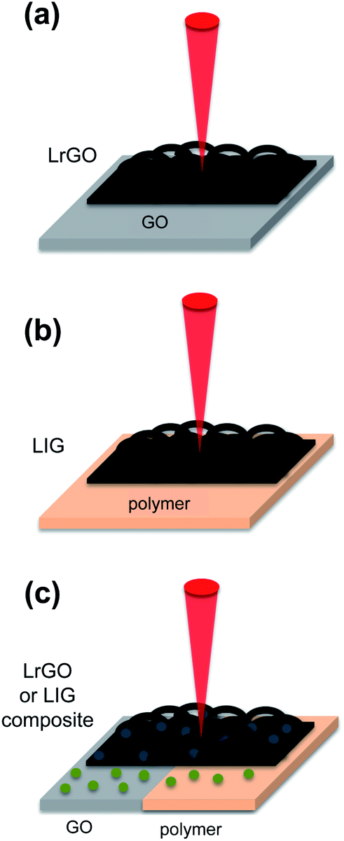 | ||
| Fig. 4 Schemes of direct laser writing (DLW) applied on (a) graphene oxide to reduce it (LrGO), (b) a polymer substrate to produce graphene (LIG), and (c) graphene oxide or a polymer substrate functionalized with a material deposited onto them (represented by the green spheres) before the laser irradiation, in order to influence the final morphology of the produced graphene or fabricate a graphene/pseudocapacitive composite in a single step. In most of the cases, the functionalizing material is chemically modified during the DLW process, as indicated by the change of the color of the spheres after laser irradiation. | ||
The main mechanisms to reduce graphene oxide by DLW are through the photochemical effect (laser wavelengths (λ) below 400 nm), the photothermal effect (laser wavelengths (λ) above 400 nm) and under certain wavelengths and irradiation conditions, through both effects.114,115 In the case of the photochemical effect, for lasers with the wavelength in the ultraviolet (UV) or near UV region, the energy of the incident photons breaks the chemical bonds of the oxygen-containing radicals that are attached to the graphene surface such as –COOH or –OH, producing LrGO. In the case of the photothermal effect, for lasers with higher wavelengths, especially in the infrared (IR) or near infrared (NIR) region, the high energy density of the incident light is absorbed by the graphene oxide and as a consequence, a very high thermal heat is concentrated locally. This generated heat breaks the chemical bonds of the oxygen-containing radicals, producing LrGO. To produce LIG from an initial polymeric substrate, a high temperature is needed to rearrange the chains into the graphene structure; therefore, lasers with wavelengths that induce the photothermal effect are required.62,116 The most commonly used polymeric substrate is commercial polyimide. However, LIG has been fabricated from a wide variety of substrates, such as wood,117 phenolic resin,118 lignin,119 polyether ether ketone (PEEK)110 or carbon nanospheres.120
The laser irradiation parameters such as the incident wavelength, power intensity, scanning speed and step size have a strong influence on the quality of the produced 3D porous graphene and its performance as a supercapacitor. Therefore, the parameters of each laser setup must be calibrated first to obtain optimized LrGO or LIG. For example, Bhattacharjya et al.121 found the optimum conditions of their system, a low-cost CO2 commercial laser (λ = 10.6 μm), under an incident power of 30 W, scanning speed of 10 mm s−1 and step size of 100 μm and the worst conditions under an incident power of 30 W, scanning speed of 500 mm s−1 and step size of 500 μm, in order to produce LrGO. This clearly means that under the same incident power, a slower scan speed and a smaller step size mean a higher irradiation time of GO and consequently, a higher removal efficiency of the oxygen-containing radicals from the graphene surface.
Currently, a CO2 commercial laser (λ = 10.6 μm) is the most widely used to produce both LrGO121,122 and LIG.123,124 Then, a pulsed laser with the wavelength in the UV region has been used in several studies in order to produce LrGO.125–129 The principal motivation to use this type of laser is that the level of reduction is very high at short times, since pulses in the order of nanoseconds/femtoseconds can produce incident powers in the order of MW. Different laser systems with intermediate wavelengths between the IR and the UV region have also been employed to produce 3D porous graphene.130–133 Similar to the DLW approach, as an attempt to maximize the rGO area in minimum time, Xiang et al.134 irradiated GO films electro-sprayed onto stainless steel sheets of 2 cm2 area for 3 min inside a home-use convection oven (far infrared irradiation) under air conditions. During the irradiation process, within which the chamber of the oven reached 200 °C, the GO film was exfoliated and the oxygen-containing functional groups were decomposed, obtaining rGO porous electrodes with a specific capacitance of 320 F g−1 at 0.2 A g−1 and a capacitance retention of 94% after 10000 cycles. Some of the recent examples with all the different lasers are summarized in Table 2, shown at the end of this section.
| Starting material | Added active material to LIG/LrGO | Final material | Laser (wavelength & writing parameters) | Capacitance | Energy density | Power density | Retention (%) after a number of cycles | Year | Ref. |
|---|---|---|---|---|---|---|---|---|---|
| Polyimide | — | LIG | 522 nm, 140 mW, 500 fs pulse, 1 MHz, 2 J cm−2, 1 mm s−1 speed | 800 μF cm−2 at 10 mV s−1 | — | — | 96% after 3000 at 0.3 mA cm−2 | 2015 | 112 |
| GO | — | LrGO | Nd:YVO4, 355 nm, 244 mW, 20 ns pulse, 0.9 kHz, 2.5 mm s−1 speed, 2.5 × 10⁻⁴ J mm−2 | 106 μF cm−2 at 0.3 V s−1 | — | — | 92.5% after 5000 at 0.6 V s−1 | 2016 | 125 |
| GO | MnO2 | LrGO + MnO2 | CO2, 10.6 μm, 2 W, 1 pass, 394 p cm−1 pulse density | 172 F g−1 at 1 mA cm−2 | 0.409 mW h cm−3 | 537 W cm−3 | 95% after 2000 at 1 mA cm−2 | 2016 | 136 |
| GO | — | LrGO | 355 nm, ns frequency, 5 m s−1 speed | 3.9 mF cm−2 at 0.3 mA cm−2 | 0.98 mW h cm−3 | 300 mW cm−3 | 93% after 20000 at 1 V s−1 |
2016 | 128 |
| GO | PEDOT | LrGO + PEDOT | IR laser 788 nm, 100 mW | 43.75 mF cm−2 at 0.2 mA cm−2 | — | — | 83.6% after 1000 at 0.2 mA cm−2 | 2017 | 130 |
| V2O5 nanobelts and GO mixture | — | LrGO + VOx | 1064 nm, 3 W, 10 μs pulse, 20 kHz, 2 m s−1 speed | 252 F g−1 at 1 A g−1 | — | — | 92% after 10000 at 100 A g−1 |
2017 | 140 |
| Polyimide | N-doping PEDOT | N-LIG + PEDOT | CO2, 10.6 μm, 5 W, 1 pass, 14 μs pulse | 790 μF cm−2 at 50 μA cm−2 | — | — | 96% after 10000 at 0.2 mA cm−2 |
2018 | 137 |
| Phenolic resin | — | LIG | 405 nm, 500 mW, 200 mm s−1 speed | 0.78 mF cm−2 at 500 mV s−1 | — | — | 93.78% after 2000 at 1 mA cm−2 | 2018 | 118 |
| Polyimide | — | LIG | Nd:YAG, 1064 nm, 7.5 A, 11 kHz, 80 mm s−1 speed | 34.7 mF cm−2 at 0.1 mA cm−2 | 1 mW h cm−3 | 11 mW cm−3 | 80% after 3000 at 0.15 mA cm−2 | 2018 | 107 |
| GO/Co3O4 nanorod mixture | — | LrGO + Co3O4 nanoparticles | KrF excimer, 248 nm, 25 ns, 10 Hz, 400 mJ per pulse per cm | 978.1 F g−1 at 1 A g−1 | — | — | 99.3% after 20000 at 10 A g−1 |
2018 | 142 |
| Lignin/PVA mixture | — | LIG | CO2, 10.6 μm, 1.8–3 W, 2.25 inches s−1 speed | 25.1 mF cm−2 at 0.05 mA cm−2 | 1 mW h cm−3 | 2 W cm−3 | 99.2% after 12000 at 2 mA cm−2 |
2018 | 119 |
| GO | — | LrGO | 308 nm, 5 MW, 105 mJ, 100 Hz | 299 F g−1 at 2 mV s−1 | — | — | 97.8% after 4000 at 50 mV s−1 | 2018 | 127 |
| GO paper | — | LrGO | Nd:YVO4 pulsed laser, 355 nm, 20 ns pulse, 325 mW, 2 mm s−1 scan speed | 13.8 μF cm−2 at 10 mV s−1 | — | — | 95% after 3400 at 10 mV s−1 | 2019 | 129 |
| ErGO | — | LrErGO | CO2, 10.6 μm, 30 W, 0.5 m s−1 speed, 20000 Hz, 1 pass |
2.32 mF cm−2 at 10 μA cm−2 | 0.46 mW h cm−2 | 0.57 W cm−2 | 100% after 100000 at 0.166 mA cm−2 |
2019 | 149 |
| GO | PANI nanofibers | LrGO + PANI | 788 nm, 5 mW, 1 pass, 25 min cycle−1 | 442 F g−1 at 0.18 A g−1 | — | — | 84% after 2000 at 3.7 A g−1 | 2019 | 139 |
| Polyimide | — | LIG | 1064 nm, 7 W, 800 mm s−1 speed | 995 mF cm−2 at 1 mA cm−2 | 55.9 μW h cm−2 | 9.39 mW cm−2 | 98% after 10000 at 1 mA cm−2 |
2019 | 131 |
| GO/urea mixture | — | N-LrGO | 1064 nm, 0.2 W, 10 ps pulse, 1 MHz, 100 mm s−1 speed | 60.7 mF cm−2 at 0.5 mA cm−2 | 6.8 μW h cm−2 | 0.25 mW cm−2 | 98.7% after 25000 at 10 mA cm−2 |
2019 | 132 |
| Carbon nanospheres | — | LIG | CO2, 10.6 μm, 3.4 W, 1 pass, 3% speed | 0.8 mF cm−2 at 0.078 mA cm−2 | 0.18 mW h cm−3 | 28 W cm−3 | 98.6% after 12000 at 1.56 mA cm−2 |
2019 | 120 |
| Polyimide coated with Mo6+, Mn2+ and S2− solution | — | LIG + MoS2 + MnS | CO2, 10.6 μm, 5–10 W, 14 μs pulse, 5–180 cm s−1 | 58.3 mF ULLK,/m−2 at 50 μA cm−2 | 7 μW h cm−2 | 49.9 μW cm−2 | 93.6% after 10000 at 1 mA cm−2 |
2019 | 145 |
| GO/TiO2 nanocrystal solution | — | LrGO + O-deficient TiO2 | KrF excimer, 248 nm, 5 Hz, 25 ns pulse, 300 mJ per pulse cm2 | 401.7 F g−1 at 1 A g−1 | 14.1 W h tkg−1 | 8.5 kW kg−1 | ≈100% after 20000 at 10 A g−1 |
2019 | 141 |
| Polyimide | PEDOT | LIG + PEDOT | CO2, 10.6 μm, 4.5 W, 20% speed, 1000 pulses per inch | 115.2 F g−1 at 0.5 A g−1 | — | — | 97.5% after 4000 at 2 A g−1 | 2020 | 138 |
| Kraft lignin | — | LIG | CO2, 10.6 μm 32 W, 20 cm s−1 speed, 1000 pulses per inch | 880 μF cm−2 at 10 mV s−2 | 0.152 μW h cm−2 | 25 μW cm−2 | 91% after 10000 at 0.02 mA cm−2 |
2020 | 124 |
| GO | PANI | LrGO + PANI | 850 nm, 1200 mW | 72 mF cm−2 at 35 μA cm−2 | 2.7 mW h cm−3 | 81.4 mW cm−3 | 93.5% after 1000 at 0.7 mA cm−2 | 2020 | 133 |
| Polyimide coated with Ni and Co ion ink | — | NiO/Co3O4/LIG | CO2, 10.6 μm 2.5 W, 100 mm s−1 speed | 29.5 mF cm−2 at 0.05 mA cm−2 | — | — | 99.1% after 10000 at 0.05 mA cm−2 |
2020 | 150 |
In the case of electrodes based on 3D porous graphene synthesized by DLW, the pseudocapacitive material fillings have another role in addition to the enhancement of the device performance: their presence minimizes the restacking of the graphene sheets during charge/discharge cycling.108,135–138 Ladrón-de-Guevara et al.139 coated LrGO (λ = 788 nm) with PANI nanofibers by electrodeposition. The composite electrode presented a specific capacitance of 442 F g−1, as opposed to the 81 F g−1 value achieved by the bare LrGO electrode, as shown in the graph of Fig. 5a. Fig. 5b to d show the scanning electron microscope (SEM) images of the electrodes in different processing stages. In Fig. 5b, a difference in the morphology before (GO) and after (LrGO) laser irradiation is observed. Fig. 5c shows a close-up image of the exfoliated and reduced GO, marked with a white area in Fig. 5b. Finally, in Fig. 5d, the densification and consequent increase of the surface area in the electrode after the deposition of PANI nanofibers can be observed as compared with the bare LrGO electrode shown in Fig. 5c.
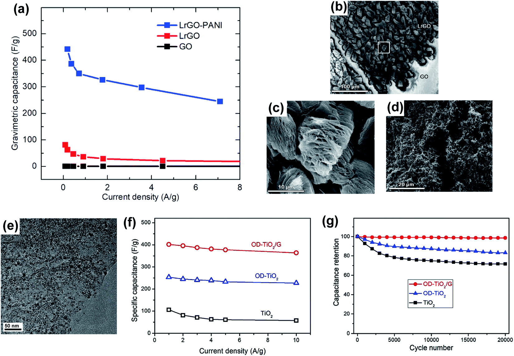 | ||
| Fig. 5 (a) Specific capacitance as a function of the current density obtained with a GO electrode (black line), a rGO electrode (red line) and a rGO/PANI nanofiber composite electrode (blue line). This comparison shows the superior performance of the rGO electrode when was coated with the PANI nanofibers. (b) SEM secondary image showing an area before (GO) and after (LrGO) the laser irradiation. (c) SEM secondary image showing an area with LrGO flakes, after laser irradiation. It corresponds to the white area marked in (b). (d) SEM image showing an area with LrGO flakes coated with PANI nanofibers after electrodeposition. (a)–(d) are reproduced with permission from ref. 139. Copyright 2018 Elsevier B.V. (e) A TEM image of an oxygen-deficient TiO2 nanocrystals/rGO composite, which shows a uniform distribution of the nanocrystals over the rGO surface. (f) Specific capacitance as a function of the current density obtained with a TiO2 electrode (black line), an oxygen-deficient TiO2 electrode (blue line) and an oxygen-deficient TiO2/rGO composite electrode (red line). This comparison was made to show the superior performance of the oxygen-deficient TiO2/rGO composite electrode with respect to the other compositions. (g) Cycling stability plot of the composites, where the oxygen-deficient TiO2/rGO composite electrode shows almost 100% capacitance retention after 20000 cycles. (e)–(g) are reproduced with permission from ref. 141. Copyright 2019 Elsevier B.V. | ||
As mentioned above and shown in Fig. 4c, DLW allows the fabrication of a 3D porous graphene/pseudocapacitive material composite in a single step, by irradiating a GO/pseudocapacitive material mixture in the case of LrGO140–142 or a polymer surface coated with a pseudocapacitive material layer in the case of LIG.143–145 Yang et al.141 irradiated a TiO2 nanocrystals/GO composite with a KrF excimer laser (λ = 248 nm, 25 ns pulse), enabling simultaneously the reduction of the GO and the creation of oxygen vacancies on the TiO2 nanocrystals. A TEM image of the final oxygen-deficient TiO2 nanocrystals/LrGO composite, presented in Fig. 5e, shows the uniform distribution of the nanocrystals over the LrGO surface. These defects were introduced to increase both the active sites and the electrical conductivity. Measuring this electrode, a specific capacitance of 400 F g−1 (Fig. 5f) and a barely disturbed capacitance retention after 20000 cycles (Fig. 5g) were obtained. Clerici et al.143 covered the initial polyimide substrate with a MoS2 dispersion and then, they irradiated the mixture with a CO2 laser, producing a MoS2 sheets/LIG composite. The introduction of an extra material into the initial mixture with GO before laser irradiation can also be done to influence the final structure of LrGO. For example, Lee et al.146 infiltrated Zn by atomic layer deposition on GO before laser irradiation. The presence of Zn influenced the morphology of the obtained LrGO by increasing the total specific surface area. The effect was a four-fold increase in the specific capacitance: from 21 F g−1 (GO → LrGO) to 83 F g−1 (GO/Zn → LrGO/Zn).
Finally, 3D porous graphene electrodes fabricated by DLW have been successfully transferred to flexible and stretchable substrates, in view of the rise of wearable and portable electronics. For example, Lamberti et al.113 developed a method to transfer LIG produced from a polyimide substrate onto polydimethylsiloxane (PDMS), as described in the scheme shown in Fig. 6a. They used the LIG/PDMS substrate to fabricate a supercapacitor (Fig. 6b), which presented a capacitance retention of 96% after 10000 cycles (Fig. 6c) under static conditions and of almost 90% after 1000 cycles under bending conditions (from 0° to 160°). Moreover, several prototypes of ‘self-charging power unit’ devices, where DLW fabricated LrGO or LIG supercapacitors were coupled to a solar cell, have been recently demonstrated.147–150 In Fig. 7a, a scheme of one of these self-powered integrated devices is shown: the LIG supercapacitor stores energy from the solar cell and illuminates an LED.149Fig. 7b shows a real device. In Fig. 7c, it is shown that the LIG-based supercapacitor presented a capacitance retention of almost 100% after 100000 cycles at 0.166 mA cm−2.
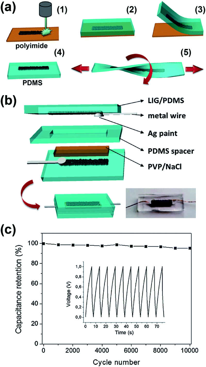 | ||
| Fig. 6 (a) Scheme of the transfer process of LIG fabricated by DLW on polyimide onto a flexible and stretchable PDMS substrate. (b) Scheme of the structure of a stretchable supercapacitor fabricated using the LIG/PDMS substrates. In the bottom right corner, the photograph of a real device is shown. (c) Cycling stability of a supercapacitor showing a capacitance retention of 96% after 10000 cycles. The graph in the inset corresponds to a set of charge/discharge cycles, which shows a highly stable performance. Reproduced with permission from ref. 113. Copyright 2016 Wiley-VCH Verlag GmbH & Co. KGaA, Weinheim. | ||
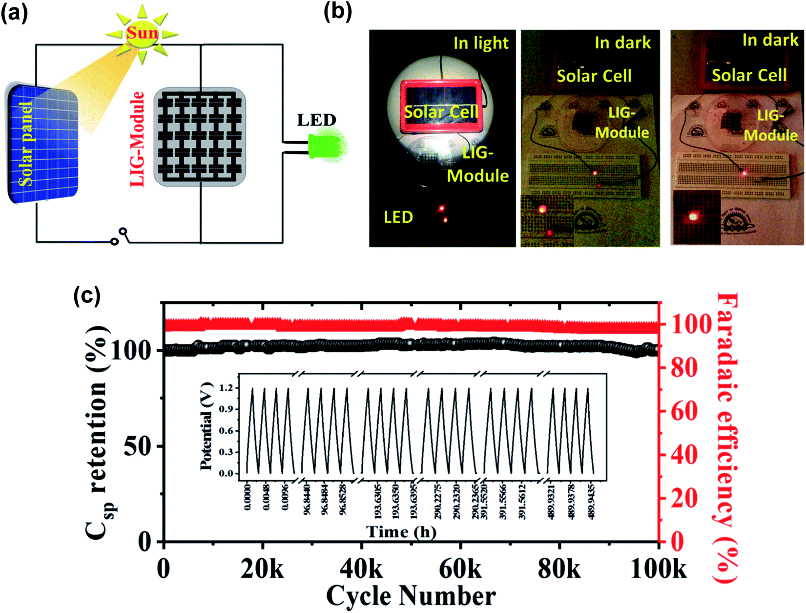 | ||
| Fig. 7 (a) Schematic drawing of a circuit including an energy storage element (based on LIG microsupercapacitors), a solar panel and an LED. (b) Labeled pictures showing the working elements of this circuit. (c) Graph showing the galvanostatic charge–discharge cycling test for the microsupercapacitor module, keeping an outstanding capacitance retention for up to 100k cycles. Reproduced with permission from ref. 149. Copyright 2019 Royal Society of Chemistry. | ||
To conclude this section, we provide Table 2, where LrGO and LIG electrodes fabricated with different laser systems and with/without added active materials to form a composite in the last few years are represented, together with the used laser system and conditions, the device performance and the corresponding references. We have ordered the electrodes in chronological order to track the evolution of the electrodes over time.
2.3 Microelectrodes
Microsupercapacitors (MSCs) are miniaturized supercapacitor devices. Compared to standard supercapacitors, MSCs use the same graphene-based materials and electrolytes, and include the same components; their performance can also be enhanced by the use of pseudocapacitive elements and their working principle is unchanged, while the scale is greatly reduced. This change in size comes not only in the in-plane dimensions, but more importantly in the out-of-plane one, its thickness. MSCs are thin-film, planar devices, a characteristic that allows them to be integrated much more easily in a variety of applications and processes, including flexible and wearable devices63 or placed alongside silicon using the same CMOS-compatible processes for on-chip energy storage.151While standard supercapacitors use sandwiched/stacked parallel electrodes in planar or rolled-up configurations for coin-like cells, MSCs are typically designed as interdigitated electrodes (IDEs), since this configuration presents several advantages over stacked ones. Fig. 8a depicts the comparison between the traditional sandwich (top) and the IDE (bottom) geometries.22 In Fig. 8b, the ion transport in both device geometries is compared as well.22 This interdigitated design is used because it provides two clear advantages, while also adding some challenges. First, it allows processing the full device on the same surface, eliminating the need for an extra assembly step, which is key for being integrated into Si-based CMOS processes on an industrial scale. It is also beneficial for ionic transport, as the perimeter of both electrodes is maximized with the number of fingers and provides a better contact and accessibility for the electrolyte. Structuring the electrode in fingers shortens ion diffusion paths, which allows for better rate performance and enables the use of certain materials that would have poor electrolyte infiltration if used in bulk. It also avoids the need of using a separator, as both electrodes are separated in-plane by a controllable gap, adding new possibilities to the design and optimization of these structures to maximize the performance. The main challenge, however, is the need to define the designed geometry for all the layers of the device, from the current collectors to the active material. This can be done through standard lithography and etching processes or through other less conventional methods, including laser ablation,152–158 mask-assisted filtration,159–162 screen printing,163,164 extrusion printing,165 electrodeposition156,166,167 and others.
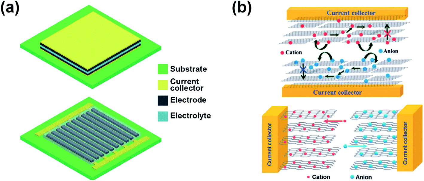 | ||
| Fig. 8 Schematic drawing of (a) two assembled microsupercapacitors (MSCs) with sandwich (top) and interdigitated (bottom) geometries, and of (b) the ion transport at the nanometric scale in both configurations: sandwich (top) and interdigitated (bottom) geometries. Reproduced with permission from ref. 22. Copyright 2014 Royal Society of Chemistry. | ||
Typically, current collectors are fabricated by lithography, by means of photoresist layer deposition, metal evaporation/sputtering and liftoff. This allows transferring the interdigitated design from an optical mask to the sample and can be done on different substrates depending on the final application. Differences arise from the deposition of the electrode materials, which are conductive porous carbons that also need to be geometrically defined. Starting from a dispersion contained in a solvent, deposition and filtration through a hard mask can create such electrodes, the limitation being the size control and resolution of this physical hard mask that needs to be machined or 3D printed. Screen printing or doctor blade coating can also be used, though they share the same limitation. Chemical vapor deposition allows depositing graphene materials from gaseous carbon precursors onto a substrate at a very high temperature and offers great control over the porosity and microstructure, and even more if plasma is added to the chamber. The huge number of parameters that can be tuned makes it a very versatile but complex process, which in most cases needs extra steps to eliminate carbon materials from the surface, as the deposition occurs in the whole surface of the substrate. Electrodeposition can also be used to form porous and conductive electrodes from graphene materials in solution, and it is also a common method to deposit pseudocapacitive elements, facilitating the production of hybrid and asymmetric devices.
Some of these carbon materials can be used as-fabricated, due to their good properties regarding conductivity, porosity and geometry definition, while others such as graphene oxide, a very common and accessible graphene material, need to be further processed. Graphene oxide in this case can be reduced chemically or thermally. Direct laser writing appears as a very versatile technique which can be used to synthesize new graphene materials (a) from polymers, as is the case of LIG,112 (b) by processing GO into LrGO58 and (c) by even processing pseudocapacitive elements, for example, modifying manganese acetate into MnO2.168 Furthermore, it can also be used to define the electrode geometry in a very precise and controlled way. When a laser is used to define the geometry of a previously processed material, the process will be referred to as ‘laser ablation’ or ‘laser etching’, while ‘laser processing’ will be used to refer to processes where the laser modifies the active electrode materials, such as LrGO or LIG.
Tiliakos et al.169 explored in 2018 the versatility of the DLW technique in order to create increasingly intricate fractal architectures which increased the perimeter of electrodes for better electrolyte accessibility, achieving 6.1 mF cm−2. In order to increase the performance of these devices, pseudocapacitive elements are added. Using environmentally friendly biomass as a precursor, Zhang et al.119 fabricated MSCs from a lignin/PVA film. The porous laser scribed lignin device achieved a surprising 25 mF cm−2 capacitance with a high power density of 8 mW cm−2 and energy density of 4 μW h cm−2. Wu et al.170 grew selectively, by solvothermal synthesis, conductive 2D metal–organic framework (MOF) structures on a LIG substrate, which acts also as the current collector in these MSCs, getting an areal capacitance of 15.2 mF cm−2 and a decent energy density of 4.1 μW h cm−2 at a high-power density of 7 mW cm−2. Similarly, but with a simpler approach, Bhattacharya et al.171 used a LIG interdigitated MSC and enhanced its performance with ‘red mud’, a mining by-product containing metallic oxides, known to be good pseudocapacitive elements. By simple dip-coating, the capacitance reached 203 mF cm−2 at 0.1 mA cm−2, with an energy density of 18 μW h cm−2 at 0.66 mW cm−2. It is important to highlight the work of Yu et al.,172 in which a commercial PI film was modified to make it more sensitive to a laser and achieve thicker 3D LIG frameworks of up to 320 μm. Adding a high mass loading of pseudocapacitive polypyrrole, the devices reached a very high energy density of 134.4 μW h cm−2 at 0.3 mW cm−2, with a great cycling stability of 95.6% at 2.5 mA cm−2 after 10000 cycles.
Direct laser writing can also be used to process and transform not only substrates, but also pseudocapacitive elements. Zhu et al.168 fabricated a LIG MSC from PEEK, a technical polymer, and afterwards deposited on top of a solution of manganese acetate, transforming it into MnO2 by a second pass of the laser. This electrode showed a high capacitance of 49 mF cm−2 and the symmetric MSC delivered a maximum energy density of 3.1 μW h cm−2 and a power density of 2.5 mW cm−2. Following a similar approach but condensing the two laser irradiations into one, Liu et al.173 and Xu et al.174 pre-treated a polyimide film with metallic precursors, which became metallic oxides at the same time as the polymer transformed into LIG. An Fe3O4 NP decorated LIG MSC achieved an outstanding capacitance of 719 mF cm−2, and an energy density of 60.2 μW h cm−2 at 0.3 mW cm−2 power density,173 while LIG with Co3O4 achieved a much higher energy density of 286.38 μW h cm−2 at a similar power.174 However, the achieved capacitance was much smaller, 1.9 mF cm−2.
Regarding the application of DLW to reduce GO and fabricate LrGO MSCs, Shen et al.175 used a femtosecond laser to define interdigitated LrGO regions with ultra-short spacing, reaching 6.3 mF cm−2 after accurately applying a gel electrolyte by laser-induced micro-droplet transfer. In a single step, Gholami et al.133 laser reduced a mixture of GO and PANI after having used a hard mask to define the IDE geometry of the drop cast slurry, achieving 72 mF cm−2 and a decent cycling stability of 93.5% at 0.7 mA cm−2 after 1000 cycles, which is still challenging for conductive polymers.
Using a hard mask to define the geometry of the device, both for contacts and active materials, is a very valid, scalable and useful method to fabricate MSCs. Couly et al.160 spray coated rGO and MXenes on a flexible substrate using a hard mask, showing that the IDE geometry achieved had better power performance than its sandwiched counterpart. Chih et al.164 used a screen printing method to deposit electrochemically exfoliated graphene and CNTs into IDEs and after adding a gel electrolyte achieved 7.7 mF cm−2, with an excellent cycling stability >99% at 200 mV s−1 after 15000 cycles. Functionalizing chemically graphene in solution was the approach used by Zhou et al.,159 who filtered through a mask a solution of fluorine-doped electrochemically exfoliated graphene, which increased the capacitance of the device up to 17,4 mF cm−2 and reached an energy density and power density of 7.67 μW h cm−2 and 2.73 mW cm−2, respectively. Again, using mask-assisted filtration, Xiao et al.161 fabricated MSCs made of exfoliated graphene, CNTs and PEDOT:PSS, on top of a pre-stretched substrate, which ensured good conductivity and porosity after relaxation. The device reached an exceptional capacitance of 107 mF cm−2.
For the cases where hard masks were not used to define the geometry of these devices, laser etching arises as a versatile technique for research, as it allows quick modification of the design for optimization and rapid prototyping. In general, laser etched devices achieve very good electrochemical properties as the focus can be kept on optimizing the material, regardless of the future interdigitated geometry that will be applied. Shao et al.152 prepared a thin film of 3D cellular graphene which after laser ablation reached 2.7 mF cm−2 but with a high-power performance of 5.3 mW cm−2. By patterning several CVD graphene monolayers via laser etching, Ye et al.155 could exploit the edge effects of the geometry and achieved 2.8 mF cm−2 by adding PANI to the device. They also used their device to demonstrate an integrated energy harvesting sensor platform. Similarly, Yoo et al.154 also exploited the edge effects of patterned heat-treated graphene oxide to fabricate a MSC with 40 mF cm−2 and an energy density of 5.4 μW h cm−2, outstanding values taking into account that no pseudocapacitive elements were added. By compositing an rGO film with polypyrrole and sputtering Au nanoparticles on top to ensure a good contact, Purkait et al.156 reached an energy density of 11.82 μW h cm−2 and a power density of 2.36 mW cm−2. By using ionic liquid electrolytes and increasing the voltage window up to 3 V, Gao et al.157 produced an outstanding laser etched rGO supercapacitor with an energy density of 32 μW h cm−2 at a power density of 1 mW cm−2.
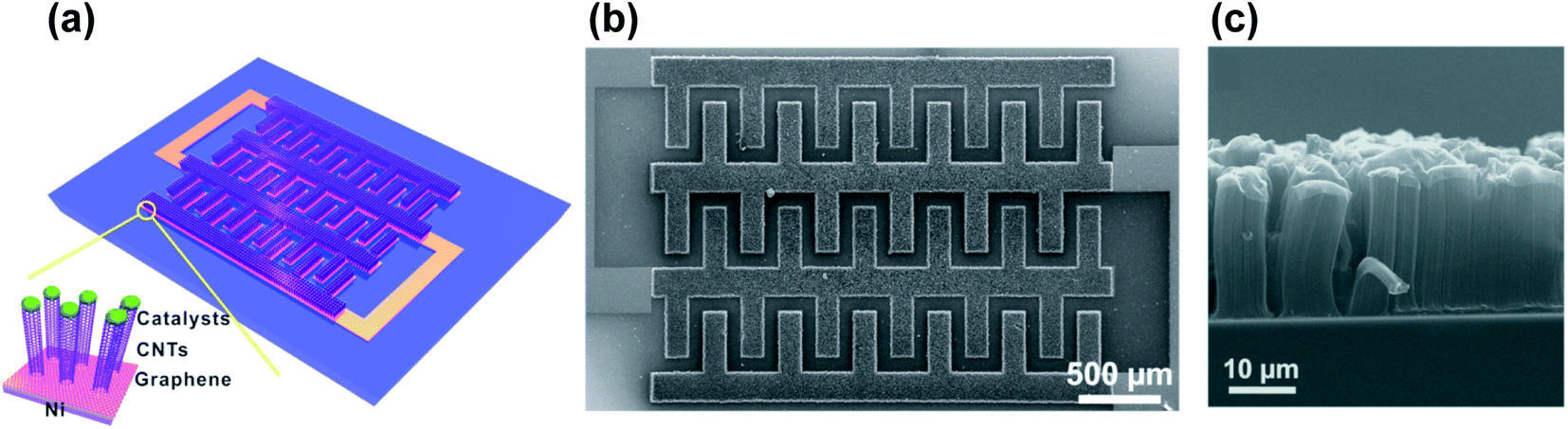
Alternative techniques are always being developed,176,177 and the MSC field is growing constantly. By interference lithography, Kim et al.178 patterned a photoresistive polymer, which after development and carbonization formed a conductive solid backbone with patterned pores for excellent electrolyte accessibility. In fact, the fabricated thick interdigitated MSC shows an outstanding power density of 165 mW cm−2, with a high energy density of 17.75 μW h cm−2. Using MEMS-based Si etching techniques to provide a 3D support for capacitive carbon materials, as Li et al. proposed,179 the fabricated supercapacitor reached remarkably high energy and power densities of 15.1 μW h cm−2 and 2.45 mW cm−2 respectively, due to a high RuOx loading and an improved hierarchical carbon microstructure on Si. Fig. 9 show an example of a hierarchic graphene/CNT-based MSC composite produced on a Si/SiO2 substrate.180 This composite was grown directly by CVD from Ni interdigitated electrodes fabricated on the Si layer by conventional photolithography. In Fig. 9a, the scheme of the device design is shown. Fig. 9b shows a SEM image of a fabricated MSC and Fig. 9c a cross-sectional SEM image of the graphene/CNT structure, grown on a Ni catalyst/electrode layer by CVD.
 | ||
| Fig. 9 (a) Schematic structure of a graphene-CNT MSC, grown on a Si substrate by chemical vapor deposition, with an inset showing the catalyst nanoparticles. (b) SEM image of the fabricated MSC, top view. (c) Cross-sectional SEM image of the graphene/CNT supercapacitor grown on a Ni catalyst/metal electrode. Reproduced with permission from ref. 180. Copyright 2012 American Chemical Society. | ||
MSCs were initially proposed to be integrated on-chip in Si-based platforms, using the CMOS technology for mass production.181 However, motivated by the rise of wearable technology, new improvements have emerged based on flexible, stretchable and bendable substrates. Thus, many of the techniques developed recently to fabricate MSCs have been applied to add a flexibility component to the performance of the device.35 Together with gel-based, quasi-solid-state, and solid-state electrolytes, these devices have demonstrated to keep their performance after cyclability bending stress tests over a large number of cycles. In Fig. 10a, several photographs show the bending of a supercapacitor at different angles.163 The cyclic voltammograms shown in Fig. 10b, taken at different bending states, show that the rectangular shape is kept regardless of the bending angle of the device. The capacitance retention under the different bending angles is also complete, compared to the value in the flat state.163 These developments pave the way for flexible supercapacitors as energy storage elements that can be easily integrated into wearable electronics.
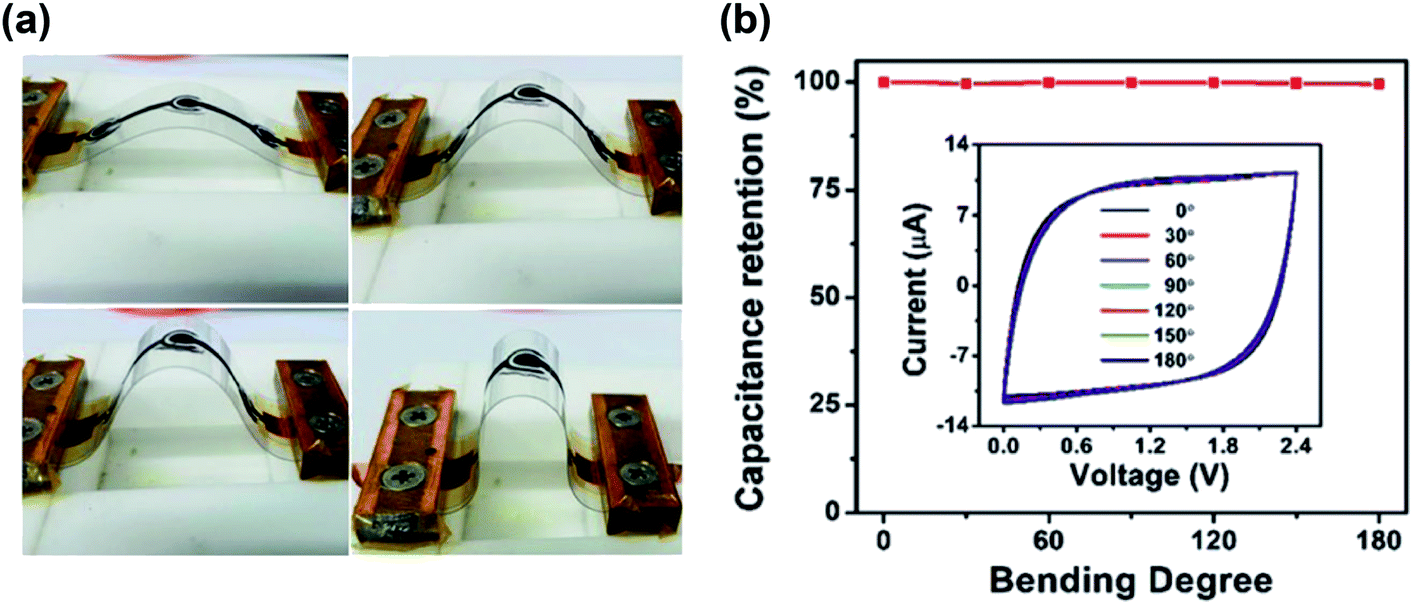 | ||
| Fig. 10 (a) Photographs of the bending cycle of a flexible microsupercapacitor at different angles. (b) Capacitance retention graph across several bending angles. The inset shows the cyclic voltammetry curves of the device at those angles, showing a very stable performance. Reproduced with permission from ref. 163. Copyright 2019 Royal Society of Chemistry. | ||
To conclude this section, we provide Table 3, where MSCs synthesized by different processes and with/without added active materials to form a composite in the last few years are represented, together with the device performance and the corresponding references. We have ordered the MSCs in chronological order to track the trend over time.
| Synthesis method | Active materials | Capacitance (mF cm−2) | Energy density (μW h cm−2) | Power density (mW cm−2) | Retention (%) after a number of cycles | Year | Ref. |
|---|---|---|---|---|---|---|---|
| Spray coating through a mask | rGO and Ti3C2Tx | 2.4 at 2 mV s−1 | 0.26 | 0.01 | 97% after 10000 at 0.2 mA cm−2 |
2017 | 160 |
| Freeze-casting assisted infiltration assembly method and laser ablation | Cellular graphene | 2.47 at 5 mV s−1 | 0.34 | 5.3 | 97.6% after 10000 at 1 mA cm−2 |
2017 | 152 |
| Electrodeposition | rGO and MnOx | 1.63 at 0.3 mA cm−2 | 0.27 | 0.19 | 85% after 1000 | 2018 | 166 |
| Electrodeposition and laser ablation | rGO, PPy and nanoporous Au | 29.21 at 0.07 mA cm−2 | 11.72 | 2.36 | 85.9% after 10000 at 5 mA cm−2 |
2018 | 156 |
| MPECVD** and Si-based microfabrication techniques | Graphene nanowall and RuO2 | 109 at 5 mV s−1 | 15.10 | 2.49 | 90.2% after 3000 at 50 mV s−1 | 2018 | 179 |
| Screen-printing with graphene ink | Screen-printed graphene | 0.89 at 5 mV s−1 | 0.91 | 0.15 | 91.8% after 10000 at 0.2 mA cm−2 |
2018 | 163 |
| DLW | LIG | 25.1 at 0.05 mA cm−2 | 4 | 8 | 98.5% after 12000 at 2 mA cm−2 |
2018 | 119 |
| Interference lithography and plasma etching | Boron-doped porous carbon | 7.15 at 100 mV s−1 | 17.75 | 165 | 85% after 12000 at 5000 mV s−1 |
2018 | 178 |
| Mask-assisted filtration of ink | Fluorine doped graphene | 17.4 at 1 mV s−1 | 7.67 | 2.73 | 93% after 5000 | 2018 | 159 |
| DLW | LIG | 6.1 at 20 mV s−1 | 0.96 | 0.25 | — | 2018 | 169 |
| CVD and laser ablation | Graphene | 45.2 at 10 mV s−1 | 0.04 | 3.17 | — | 2018 | 155 |
| Mask-assisted filtration of ink | Graphene, CNTs and PEDOT | 107.5 at 5 mV s−1 | 1.27 | 0.12 | — | 2018 | 161 |
| 0.54 | 1.22 | ||||||
| DLW | LrGO | 6.3 at 1 mV s−1 | 0.09 | 0.60 | 100% after 1000 at 500 mV s−1 | 2018 | 175 |
| 0.42 | 0.00 | ||||||
| Biomimetic microfluidic fabrication | rGO and metallic MoS2 microfibers | 48.4 at 1 V s−1 | 4 | 40 | 97% after 10000 |
2018 | 176 |
| Conventional lithographic techniques and laser ablation | rGO | 40 at 10 mV s−1 | 5.40 | 1.48 | 83.5% after 10000 at 100 mV s−1 |
2018 | 154 |
| Freeze-drying and laser ablation | rGO and Ti3C2Tx aerogel | 34.6 at 1 mV s−1 | 2.18 | 0.06 | 91% after 15000 at 2 mA cm−2 |
2018 | 153 |
| 1.33 | 0.18 | ||||||
| Ion-liquid reduction and laser ablation | rGO and carbon paper | 27.4 at 0.7 mA cm−2 | 32.10 | 1.05 | — | 2019 | 157 |
| 27.40 | 1.65 | ||||||
| Screen-printing | Graphene and CNTs | 7.7 at 5 mV s−1 | 1.07 | 0.32 | > 99% after 15000 at 200 mV s−1 |
2019 | 164 |
| DLW | LIG and Ni-catecholate MOF*** nanorods | 15.2 at 0.2 mA cm−2 | 4.1 | 7 | 87% after 5000 at 2 mA cm−2 | 2019 | 170 |
| Slurry coating and laser ablation. Electrodeposition. | n-doped graphene and MnO2 | 13.3 at 0.25 mA cm−2 | 5.88 | 1.13 | 84% after 5000 at 2 A g−1 | 2019 | 158 |
| DLW | LIG and MnO2 | 48.9 at 10 mV s−1 | 3.1 | 2.5 | 94.3% after 3000 at 0.5 mA cm−2 | 2020 | 168 |
| DLW | LIG and Fe3O4 nanoparticles | 719.28 at 1 mV s−1 | 60.2 | 0.3 | 74% after 900 at 20 mV s−1 | 2020 | 173 |
| 10 | 0.75 | ||||||
| DLW | LIG and Co3O4 | 10.9 at 5 mV s−1 | 286.38 | 0.43 | 97.8% after 10000 at 0.08 mA cm−2 |
2020 | 174 |
| 10.94 | 0.7 | ||||||
| DLW | LIG and PPy | 2412.2 at 0.5 mA cm−2 | 134.4 | 0.325 | 95.6% after 10000 at 2.5 mA cm−2 |
2020 | 172 |
| DLW | LIG and red-mud | 203 at 0.1 mA cm−2 | 18 | 0.66 | 81% 4000 at 0.3 mA cm−2 | 2020 | 171 |
| 2 | 1.36 | ||||||
| Drop casting over carbon fiber. Electrodeposition | rGO, PEDOT:PSS and MnO2 | 550 at 3 mA cm−2 | 295 | 2.9 | 95% after 5000 at 12 mA cm−2 | 2020 | 167 |
| 150 | 14.1 | ||||||
| Mask-assisted deposition | EG + CNT + rGO/PPy | 38 at 1 mV s−1 | 0.306 | 0135 | 82% after 4500 | 2020 | 162 |
| Slurry coating on an imprinted substrate | GO, graphene aerogel and MnO2 | 14.2 at 10 mV s−1 | 1.2 | 0.043 | 85% after 25000 |
2020 | 177 |
| 0.66 | 0.436 |
3 Results and discussion: Ragone plots of the latest graphene-based supercapacitors
Graphene supercapacitors are rapidly evolving from laboratory prototypes to final devices that will complement or even perhaps compete with commercial batteries in the near future. This is because their properties and performance have greatly improved over the last decade. The three technologies that have contributed the most to their development, namely, graphene foam, laser reduction and microsupercapacitors, have been reviewed in detail and are summarized below.Graphene foam made by CVD from sacrificial templates enables making high capacity electrodes for large area supercapacitors, with a demonstrated gravimetric capacitance of up to 2585 F g−1 (ref. 100) and a capacitance retention of 96.5% after 10000 cycles.90 Graphene provides high electrical conductivity and its porous structure presents a large surface area and allows an easy transit of electrolyte ions. In this way, a light and flexible 3D electrode can be obtained. DLW represents a low-cost, fast, and single step technique to produce large area and flexible electrodes based on laser reduced GO or laser induced graphene. Despite achieving electrodes with very good capacitance retention (see Table 2), the laser wavelength and processing parameters required to produce supercapacitors with higher specific capacitance than those using graphene foam fabricated by CVD have not been optimized yet. All these graphene forms, namely, graphene foam, LrGO and LIG, have an empty pore area that can be functionalized with various pseudocapacitive materials. The most widely used so far are metallic oxides and conductive polymers, although recently transition metal sulfides are being explored to push further the achievable power density, cycling stability and operating voltage window.
Miniaturized supercapacitors, or MSCs, are becoming increasingly popular due to their integration possibilities. The rise of wearable electronics is driving this approach to grow rapidly, and scaling down the supercapacitor technology to the microscale has revealed some advantages. The use of IDEs eases ion accessibility, improving power performance, and gel and solid-state electrolytes allow these devices to be easily encapsulated in bendable or stretchable modules. Electrodes can be fabricated by scalable, cheap and quick processes such as screen printing or drop casting, and can be grown on top of or transferred to almost any target substrate. Laser writing has emerged recently as a quick and easy way to fabricate supercapacitor electrodes from inexpensive materials and to pattern them easily into interdigitated microsupercapacitor electrodes. This flexibility is ideal for their integration into the growing industry of wearable electronics, where MSCs are expected to play a crucial role in the future.
As the Ragone plot in Fig. 11a shows, the energy and power density of new supercapacitor devices are already approaching energy density performances that were typically restricted to batteries, but with better power performance. Each dot in this graph represents an energy-power working point of the fabricated devices included in Table 1. Most of these devices have been fabricated using graphene foam of CVD graphene or rGO, but are always complemented with pseudocapacitive elements. CVD graphene shows a more open-pore interconnected network and is of very high quality, while several key properties depend to great extent on the metallic foam template on which it is grown, such as the surface area, or the pore size and distribution. On the other hand, rGO typically creates compact 3D porous structures with smaller pores and a higher surface area, while being less accessible to the electrolyte and having worse electrical properties than CVD graphene. However, our comparison shows that both CVD graphene and rGO are very competitive materials for the fabrication of supercapacitor devices, showing comparable results in the Ragone plot shown in Fig. 11a. However, differences regarding the pseudocapacitive elements included in these devices are more clearly highlighted in that same graph. The recent literature has reported a large number of devices that use, in order to achieve the best performance, mostly bimetallic oxides and sulfides, as well as other materials including hydroxides, as pseudocapacitive elements. The use of metallic and bimetallic sulfides (green dots) has been showing the best results when compared to their oxide counterpart (orange triangles), and these devices show already a comparable, if not better, working point to that stated by Simon and Gogotsi for batteries in their recent review of the field.5 It is important to note that the red area of Fig. 11a and the blue area, taken from the Simon and Gogotsi article, only include commercial devices, and the dots are exclusively plotted from the data of research papers published during the last 3 years. This shows the strength of the supercapacitor technology, which can not only complement, but also compete directly with batteries regarding energy density and power density, showing much better cycling stabilities and being fabricated from materials less scarce than lithium.
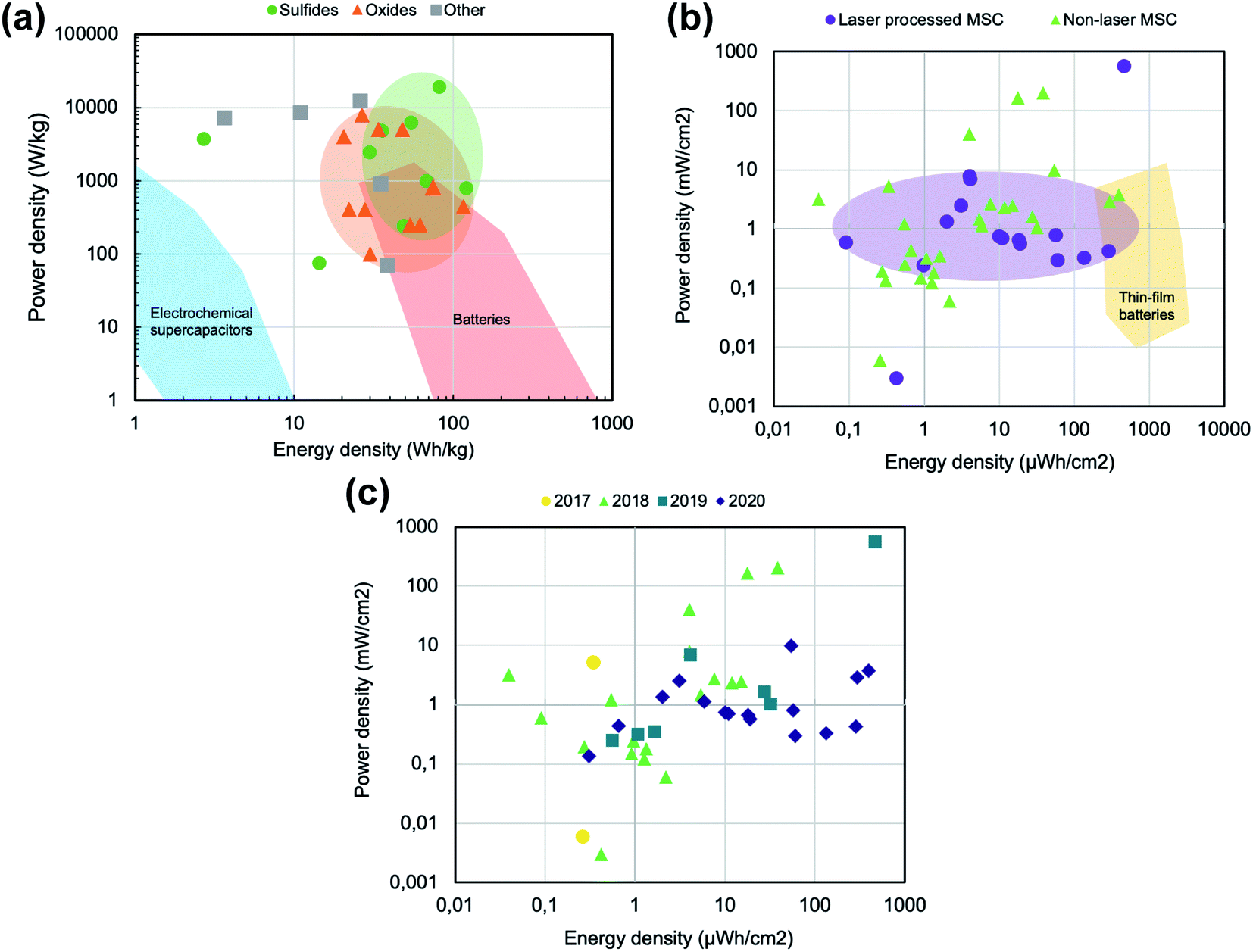 | ||
| Fig. 11 (a) Schematic gravimetric Ragone plot where the typical working regions for commercial supercapacitors and batteries are highlighted. Each dot represents one working point of a graphene-foam based device classified by the type of its active pseudocapacitive material, green for sulfides, orange for oxides and grey for other compounds, such as metal hydroxides or metallic nanoparticles. (b) Schematic areal Ragone plot. Each dot represents one thin-film device reported in the literature, purple for laser processed micro-supercapacitors and green for non-laser microsupercapacitors. The yellow region represents the typical working point of thin-film batteries as reported by ref. 182. (c) Schematic areal Ragone plot of the same data used in Fig. 11b, classified by the publishing date. | ||
This gravimetric classification includes graphene foam-based devices, which typically are reported using per-kg metrics. However, for thin film devices such as microsupercapacitors, figures-of-merit are typically given in areal or volumetric terms, as they are fabricated with thicknesses in the range of a few μm. Its mass is not really the defining factor limiting its performance, but its area. Fig. 11b shows this classification in an areal Ragone plot, where every dot represents one energy-power working point of a fabricated microsupercapacitor device as reported in the literature (references shown in Tables 2 and 3). There is growing interest in laser processing technology, due to its multiple advantages regarding flexibility, speed and low-cost. In the past two years, the number of papers published using laser writing to process supercapacitor materials has grown a lot, almost monopolizing all recent research in the field. Most of the papers found in the literature which used non-laser processes to fabricate microsupercapacitors were mostly published in 2018 and before, using techniques such as mask-assisted filtration, screen printing or standard lithography to define the interdigitated geometries. However, from 2019, mostly laser-processed microsupercapacitors have been found. This classification of the results by year can be seen in Fig. 11c.
Regarding electrochemical performance, and despite all this recent interest, laser processed MSCs, shown as purple dots in Fig. 11b, show a saturation of the power density in the 10 mW cm−2 range, going even lower for the most energy dense performances, towards the 1 mW cm−2 limit. This could be due to the lower quality of the materials that can be achieved through laser processing, be it laser induced graphene from polymeric films or laser-reduced graphene oxide from graphene oxide films. However, the energy density of these devices has been steadily increasing since 2017, and some recent devices lay in a working range very close to that of thin film batteries, devices comparable to microsupercapacitors in their metrics. By compositing these laser-processed graphene materials with pseudocapacitive elements, for example Co3O4 (ref. 174) or Fe3O4 (ref. 173), the energy density is being pushed towards the thin film battery region, which are the best performing devices in terms of areal energy density nowadays.182
4 Conclusion and outlook
In summary, to move the supercapacitor and MSC field forward, DLW processing has recently emerged as a very promising technique. This technique allows quick, one-step processing to create a highly porous and conductive 3D network of graphene sheets, using commercial laser systems. Building up from technologies such as 3D printers and laser cutters, these systems demonstrate great scalability and increasing precision, as well as industrial availability. Furthermore, structuring these materials into IDEs helps electrolyte accessibility and could allow for better power performance. However, most of the recent work in the field has focused on increasing its energy density towards the thin-film battery range, and it will be a challenge for the following years to further increase the power density. On top of this, synergies are appearing and can be exploited, as some studies suggest the advantages of using laser processing for both the graphene material and the pseudocapacitive element. This combined process can, for example, add oxygen vacancies to metal oxides or transform through photochemistry conductive polymers, which could be used together with graphene materials fabricated using new laser 3D printer systems. However, there are still some challenges that need to be overcome for the widespread use of graphene-based supercapacitors. First, the large-scale fabrication of porous graphene materials with high quality and uniformity must be ensured. Optimization is still needed in several areas, such as the intimate contact and adherence of pseudocapacitive elements on the graphene network, or the choice of an ideal pseudocapacitive material and its possible synergies with the electrolyte for an optimized voltage window and cyclability. Minimizing the agglomeration and restacking of the graphene sheets is a problem present in all-carbon EDLCs that must be addressed, while in the case of pseudocapacitors, it can be done by intercalating the graphene material with active nanoparticles.If the expectations are met, graphene supercapacitors and microsupercapacitors are meant to become a competitive complement, or even alternative, to traditional lithium ion batteries and thin film batteries, as well as an essential component in new wearable and portable electronic devices.
Conflicts of interest
There are no conflicts of interest to declare.Acknowledgements
A. Velasco is in receipt of an FPU grant from the Spanish Government. This work was supported by Spanish Ministerio de Economía y Competitividad (MINECO), project DIGRAFEN (ENE2017-88065-C2-1-R) (MINECO/AEI/FEDER, UE) and from the Comunidad de Madrid through project NMAT2D-CM (P2018/NMT-4511). J. Pedrós acknowledges financial support from MINECO (Grant RyC-2015-18968) and UPM (Ayuda para la incorporación y retención de talento doctor, Programa Propio de I+D+i 2019 y 2020).References
- R. Kotz and M. Carlen, Electrochim. Acta, 2000, 45, 2483–2498 CrossRef CAS.
- M. Winter and R. J. Brodd, Chem. Rev., 2004, 104, 4245–4269 CrossRef CAS.
- J. Yan, Q. Wang, T. Wei and Z. Fan, Adv. Energy Mater., 2014, 4(4), 1300816 CrossRef.
- P. Simon, Y. Gogotsi and B. Dunn, Science, 2014, 343, 1210–1211 CrossRef CAS.
- P. Simon and Y. Gogotsi, Nat. Mater., 2020, 19, 1151–1163 CrossRef CAS.
- Z. Lin, E. Goikolea, A. Balducci, K. Naoi, P. L. Taberna, M. Salanne, G. Yushin and P. Simon, Mater. Today, 2018, 21, 419–436 CrossRef CAS.
- L. Kouchachvili, W. Yaïci and E. Entchev, J. Power Sources, 2018, 374, 237–248 CrossRef CAS.
- X. Dai, F. Wan, L. Zhang, H. Cao and Z. Niu, Energy Storage Mater., 2019, 17, 143–150 CrossRef.
- D. P. Dubal, N. R. Chodankar, D. H. Kim and P. Gomez-Romero, Chem. Soc. Rev., 2018, 47, 2065–2129 RSC.
- X. Chen, N. S. Villa, Y. Zhuang, L. Chen, T. Wang, Z. Li and T. Kong, Adv. Energy Mater., 2020, 10, 1902769 CrossRef CAS.
- Q. Zhang, J. Sun, Z. Pan, J. Zhang, J. Zhao, X. Wang, C. Zhang, Y. Yao, W. Lu, Q. Li, Y. Zhang and Z. Zhang, Nano Energy, 2017, 39, 219–228 CrossRef CAS.
- Q. Zhang, W. Xu, J. Sun, Z. Pan, J. Zhao, X. Wang, J. Zhang, P. Man, J. Guo, Z. Zhou, B. He, Z. Zhang, Q. Li, Y. Zhang, L. Xu and Y. Yao, Nano Lett., 2017, 17, 7552–7560 CrossRef CAS.
- Z. Zhou, Q. Zhang, J. Sun, B. He, J. Guo, Q. Li, C. Li, L. Xie and Y. Yao, ACS Nano, 2018, 12, 9333–9341 CrossRef CAS.
- K. B. Oldham, J. Electroanal. Chem., 2008, 613, 131–138 CrossRef CAS.
- B. E. Conway, Electrochemical Supercapacitors: Scientific Fundamentals and Technological Applications, Springer US, 1st edn Search PubMed.
- Q. Meng, K. Cai, Y. Chen and L. Chen, Nano Energy, 2017, 36, 268–285 CrossRef CAS.
- Y. Jiang and J. Liu, Energy Environ. Mater., 2019, 2, 30–37 CrossRef.
- B. Pal, S. Yang, S. Ramesh, V. Thangadurai and R. Jose, Nanoscale Adv., 2019, 1, 3807–3835 RSC.
- C. Zhong, Y. Deng, W. Hu, J. Qiao, L. Zhang and J. Zhang, Chem. Soc. Rev., 2015, 44, 7484–7539 RSC.
- M. D. Stoller and R. S. Ruoff, Energy Environ. Sci., 2010, 3, 1294–1301 RSC.
- A. Noori, M. F. El-Kady, M. S. Rahmanifar, R. B. Kaner and M. F. Mousavi, Chem. Soc. Rev., 2019, 48, 1272–1341 RSC.
- M. Beidaghi and Y. Gogotsi, Energy Environ. Sci., 2014, 7, 867–884 RSC.
- H. Li, C. Qi, Y. Tao, H. Liu, D. W. Wang, F. Li, Q. H. Yang and H. M. Cheng, Adv. Energy Mater., 2019, 9, 1900079 CrossRef.
- C. Backes, A. M. Abdelkader, C. Alonso, A. Andrieux-Ledier, R. Arenal, J. Azpeitia, N. Balakrishnan, L. Banszerus, J. Barjon, R. Bartali, S. Bellani, C. Berger, R. Berger, M. M. B. Ortega, C. Bernard, P. H. Beton, A. Beyer, A. Bianco, P. Bøggild, F. Bonaccorso, G. B. Barin, C. Botas, R. A. Bueno, D. Carriazo, A. Castellanos-Gomez, M. Christian, A. Ciesielski, T. Ciuk, M. T. Cole, J. Coleman, C. Coletti, L. Crema, H. Cun, D. Dasler, D. De Fazio, N. Díez, S. Drieschner, G. S. Duesberg, R. Fasel, X. Feng, A. Fina, S. Forti, C. Galiotis, G. Garberoglio, J. M. García, J. A. Garrido, M. Gibertini, A. Gölzhäuser, J. Gómez, T. Greber, F. Hauke, A. Hemmi, I. Hernandez-Rodriguez, A. Hirsch, S. A. Hodge, Y. Huttel, P. U. Jepsen, I. Jimenez, U. Kaiser, T. Kaplas, H. K. Kim, A. Kis, K. Papagelis, K. Kostarelos, A. Krajewska, K. Lee, C. Li, H. Lipsanen, A. Liscio, M. R. Lohe, A. Loiseau, L. Lombardi, M. F. López, O. Martin, C. Martín, L. Martínez, J. A. Martin-Gago, J. I. Martínez, N. Marzari, Á. Mayoral, J. McManus, M. Melucci, J. Méndez, C. Merino, P. Merino, A. P. Meyer, E. Miniussi, V. Miseikis, N. Mishra, V. Morandi, C. Munuera, R. Muñoz, H. Nolan, L. Ortolani, A. K. Ott, I. Palacio, V. Palermo, J. Parthenios, I. Pasternak, A. Patane, M. Prato, H. Prevost, V. Prudkovskiy, N. Pugno, T. Rojo, A. Rossi, P. Ruffieux, P. Samorì, L. Schué, E. Setijadi, T. Seyller, G. Speranza, C. Stampfer, I. Stenger, W. Strupinski, Y. Svirko, S. Taioli, K. B. K. Teo, M. Testi, F. Tomarchio, M. Tortello, E. Treossi, A. Turchanin, E. Vazquez, E. Villaro, P. R. Whelan, Z. Xia, R. Yakimova, S. Yang, G. R. Yazdi, C. Yim, D. Yoon, X. Zhang, X. Zhuang, L. Colombo, A. C. Ferrari and M. Garcia-Hernandez, 2D Mater., 2020, 7, 022001 CrossRef CAS.
- M. D. Stoller, S. Park, Z. Yanwu, J. An and R. S. Ruoff, Nano Lett., 2008, 8, 3498–3502 CrossRef CAS.
- B. Kelly, Physics of Graphite: Applied Science Publishers, London Englewood N.J, 1981 Search PubMed.
- S. V. Morozov, K. S. Novoselov, M. I. Katsnelson, F. Schedin, D. C. Elias, J. A. Jaszczak and A. K. Geim, Phys. Rev. Lett., 2008, 100, 016602 CrossRef CAS.
- A. Boscá, J. Pedrós, J. Martínez and F. Calle, J. Appl. Phys., 2015, 117(4), 044504 CrossRef.
- K. S. Novoselov, A. K. Geim, S. V. Morozov, D. Jiang, Y. Zhang, S. V. Dubonos, I. V. Grigorieva and A. A. Firsov, Science, 2004, 306, 666–669 CrossRef CAS.
- C. Si, Z. Sun and F. Liu, Nanoscale, 2016, 8, 3207–3217 RSC.
- M. F. El-Kady, Y. Shao and R. B. Kaner, Nat. Rev. Mater., 2016, 1, 16033 CrossRef CAS.
- X. Cao, Z. Yin and H. Zhang, Energy Environ. Sci., 2014, 7, 1850–1865 RSC.
- V. Chabot, D. Higgins, A. Yu, X. Xiao, Z. Chen and J. Zhang, Energy Environ. Sci., 2014, 7, 1564–1596 RSC.
- Y. Wu, J. Zhu and L. Huang, Carbon, 2019, 143, 610–640 CrossRef CAS.
- L. Dong, C. Xu, Y. Li, Z. H. Huang, F. Kang, Q. H. Yang and X. Zhao, J. Mater. Chem. A, 2016, 4, 4659–4685 RSC.
- Y. Zhu, S. Murali, M. D. Stoller, K. J. Ganesh, W. Cai, P. J. Ferreira, A. Pirkle, R. M. Wallace, K. A. Cychosz, M. Thommes, D. Su, E. A. Stach and R. S. Ruoff, Science, 2011, 332, 1537–1541 CrossRef CAS.
- B. G. Choi, M. Yang, W. H. Hong, J. W. Choi and Y. S. Huh, ACS Nano, 2012, 6, 4020–4028 CrossRef CAS.
- Z. Niu, J. Chen, H. H. Hng, J. Ma and X. Chen, Adv. Mater., 2012, 24, 4144–4150 CrossRef CAS.
- H. C. Tao, S. C. Zhu, X. L. Yang, L. L. Zhang and S. B. Ni, Electrochim. Acta, 2016, 190, 168–177 CrossRef CAS.
- X. Cao, Y. Shi, W. Shi, G. Lu, X. Huang, Q. Yan, Q. Zhang and H. Zhang, Small, 2011, 7, 3163–3168 CrossRef CAS.
- P. Romero, P. A. Postigo, E. Baquedano, J. Martínez, A. Boscá and R. Guzman de Villoria, Chem. Eng. J., 2016, 299, 8–14 CrossRef CAS.
- A. Boscá, J. Pedrós, J. Martínez, T. Palacios and F. Calle, Sci. Rep., 2016, 6, 21676 CrossRef.
- S. Fernández, A. Boscá, J. Pedrós, A. Inés, M. Fernández, I. Arnedo, J. P. González, M. de la Cruz, D. Sanz, A. Molinero, R. S. Fandan, M. ángela Pampillón, F. Calle, J. J. Gandía, J. Cárabe and J. Martínez, Micromachines, 2019, 10, 402 CrossRef.
- Z. Fan, J. Yan, L. Zhi, Q. Zhang, T. Wei, J. Feng, M. Zhang, W. Qian and F. Wei, Adv. Mater., 2010, 22, 3723–3728 CrossRef CAS.
- D. Yu and L. Dai, J. Phys. Chem. Lett., 2010, 1, 467–470 CrossRef CAS.
- B. You, L. Wang, L. Yao and J. Yang, Chem. Commun., 2013, 49, 5016–5018 RSC.
- J. Chang, M. Jin, F. Yao, T. H. Kim, V. T. Le, H. Yue, F. Gunes, B. Li, A. Ghosh, S. Xie and Y. H. Lee, Adv. Funct. Mater., 2013, 23, 5074–5083 CrossRef CAS.
- Q. Cheng, J. Tang, J. Ma, H. Zhang, N. Shinya and L. C. Qin, Carbon, 2011, 49, 2917–2925 CrossRef CAS.
- H. Wang, H. Yi, X. Chen and X. Wang, J. Mater. Chem. A, 2014, 2, 3223–3230 RSC.
- J. Yan, Z. Fan, W. Sun, G. Ning, T. Wei, Q. Zhang, R. Zhang, L. Zhi and F. Wei, Adv. Funct. Mater., 2012, 22, 2632–2641 CrossRef CAS.
- D. S. Patil, S. A. Pawar, J. C. Shin and H. J. Kim, J. Power Sources, 2019, 435, 226812 CrossRef CAS.
- S. Liu, Y. Yin, K. San Hui, K. N. Hui, S. C. Lee and S. Chan Jun, Electrochim. Acta, 2019, 297, 479–487 CrossRef CAS.
- S. Ruiz-Gómez, A. Boscá, L. Pérez, J. Pedrós, J. Martínez, A. Páez and F. Calle, Diamond Relat. Mater., 2015, 57, 63–67 CrossRef.
- K. Zhang, L. L. Zhang, X. S. Zhao and J. Wu, Chem. Mater., 2010, 22, 1392–1401 CrossRef CAS.
- Q. Wu, X. Yuxi, Z. Yao, A. Liu and G. Shi, ACS Nano, 2010, 4, 1963–1970 CrossRef CAS.
- Y. Gao, Nanoscale Res. Lett., 2017, 12, 387 CrossRef.
- J. Pedrós, A. Boscá, J. Martínez, S. Ruiz-Gómez, L. Pérez, V. Barranco and F. Calle, J. Power Sources, 2016, 317, 35–42 CrossRef.
- M. F. El-Kady, V. Strong, S. Dubin and R. B. Kaner, Science, 2012, 335, 1326–1330 CrossRef CAS.
- M. F. El-Kady and R. B. Kaner, Nat. Commun., 2013, 4, 1475 CrossRef.
- L. Li, J. Zhang, Z. Peng, Y. Li, C. Gao, Y. Ji, R. Ye, N. D. Kim, Q. Zhong, Y. Yang, H. Fei, G. Ruan and J. M. Tour, Adv. Mater., 2016, 28, 838–845 CrossRef CAS.
- Z. Wan, E. W. Streed, M. Lobino, S. Wang, R. T. Sang, I. S. Cole, D. V. Thiel and Q. Li, Adv. Mater. Technol., 2018, 3, 1700315 CrossRef.
- X. Y. Fu, Z. Di Chen, D. D. Han, Y. L. Zhang, H. Xia and H.-B. Sun, Photon. Res., 2020, 8, 577–588 CrossRef CAS.
- J. Wang, F. Li, F. Zhu and O. G. Schmidt, Small Methods, 2019, 3, 1800367 Search PubMed.
- Z. Chen, W. Ren, L. Gao, B. Liu, S. Pei and H. M. Cheng, Nat. Mater., 2011, 10, 424–428 CrossRef CAS.
- S. Min, C. Zhao, G. Chen and X. Qian, Electrochim. Acta, 2014, 115, 155–164 CrossRef CAS.
- J. Yang, E. Zhang, X. Li, Y. Yu, J. Qu and Z. Z. Yu, ACS Appl. Mater. Interfaces, 2016, 8, 2297–2305 CrossRef CAS.
- X. Li, Z. Wang, Y. Qiu, Q. Pan and P. Hu, J. Alloys Compd., 2015, 620, 31–37 CrossRef CAS.
- J. Lv, Z. Wang and H. Miura, Solid State Commun., 2018, 269, 45–49 CrossRef CAS.
- G. Ren, R. Zhang and Z. Fan, Appl. Surf. Sci., 2018, 441, 466–473 CrossRef CAS.
- N. Van Hoa, T. T. H. Quyen, N. H. Nghia, N. Van Hieu and J. J. Shim, J. Alloys Compd., 2017, 702, 693–699 CrossRef.
- L. Jinlong, Z. Wang, L. Tongxiang, Y. Meng, K. Suzuki and H. Miura, J. Electroanal. Chem., 2017, 799, 595–601 CrossRef.
- X. Dong, J. Wang, J. Wang, M. B. Chan-Park, X. Li, L. Wang, W. Huang and P. Chen, Mater. Chem. Phys., 2012, 134, 576–580 CrossRef CAS.
- Y. Zhao, J. Liu, Y. Hu, H. Cheng, C. Hu, C. Jiang, L. Jiang, A. Cao and L. Qu, Adv. Mater., 2013, 25, 591–595 CrossRef CAS.
- J. Ren, R. P. Ren and Y. K. Lv, Chem. Eng. J., 2018, 349, 111–118 CrossRef CAS.
- J. Zhu, L. Kong, X. Shen, Q. Chen, Z. Ji, J. Wang, K. Xu and G. Zhu, Appl. Surf. Sci., 2018, 428, 348–355 CrossRef CAS.
- Q. Li, M. Horn, Y. Wang, J. MacLeod, N. Motta and J. Liu, Materials, 2019, 12, 703 CrossRef CAS.
- X. Bai, Q. Liu, H. Zhang, J. Liu, Z. Li, X. Jing, Y. Yuan, L. Liu and J. Wang, Electrochim. Acta, 2016, 215, 492–499 CrossRef CAS.
- T. Yin, W. Zhang, Y. Yin, Y. Yan, K. Zhan, J. Yang and B. Zhao, J. Mater. Sci.: Mater. Electron., 2017, 28, 7884–7891 CrossRef CAS.
- M. Yu, J. Chen, J. Liu, S. Li, Y. Ma, J. Zhang and J. An, Electrochim. Acta, 2015, 151, 99–108 CrossRef CAS.
- S. Sun, S. Wang, S. Li, Y. Li, Y. Zhang, J. Chen, Z. Zhang, S. Fang and P. Wang, J. Mater. Chem. A, 2016, 4, 18646–18653 RSC.
- C. Zhang, T. Kuila, N. H. Kim, S. H. Lee and J. H. Lee, Carbon, 2015, 89, 328–339 CrossRef CAS.
- J. Lv, T. Liang, M. Yang, S. Ken and M. Hideo, J. Energy Chem., 2017, 26, 330–335 CrossRef.
- X. Feng, J. Ning, D. Wang, J. Zhang, M. Xia, Y. Wang and Y. Hao, J. Alloys Compd., 2020, 816, 152625 CrossRef CAS.
- H. Chen, C. K. Hsieh, Y. Yang, X. Y. Liu, C. H. Lin, C. H. Tsai, Z. Q. Wen, F. Dong and Y. X. Zhang, ChemElectroChem, 2017, 4, 2414–2422 CrossRef CAS.
- L. H. Tseng, C. H. Hsiao, D. D. Nguyen, P. Y. Hsieh, C. Y. Lee and N. H. Tai, Electrochim. Acta, 2018, 266, 284–292 CrossRef CAS.
- Z. Zhang, K. Chi, F. Xiao and S. Wang, J. Mater. Chem. A, 2015, 3, 12828–12835 RSC.
- X. Bai, Q. Liu, J. Liu, Z. Gao, H. Zhang, R. Chen, Z. Li, R. Li, P. Liu and J. Wang, Chem. Eng. J., 2017, 328, 873–883 CrossRef CAS.
- K. Chi, Z. Zhang, Q. Lv, C. Xie, J. Xiao, F. Xiao and S. Wang, ACS Appl. Mater. Interfaces, 2017, 9, 6044–6053 CrossRef CAS.
- A. A. Mirghni, M. J. Madito, K. O. Oyedotun, T. M. Masikhwa, N. M. Ndiaye, S. J. Ray and N. Manyala, RSC Adv., 2018, 8, 11608–11621 RSC.
- G. Saeed, S. Kumar, N. H. Kim and J. H. Lee, Chem. Eng. J., 2018, 352, 268–276 CrossRef CAS.
- L. G. Beka, X. Li and W. Liu, Sci. Rep., 2017, 7, 2105 CrossRef.
- M. Yu, X. Li, Y. Ma, R. Liu, J. Liu and S. Li, Appl. Surf. Sci., 2017, 396, 1816–1824 CrossRef CAS.
- P. Miao, J. He, Z. Sang, F. Zhang, J. Guo, D. Su, X. Yan, X. Li and H. Ji, J. Alloys Compd., 2018, 732, 613–623 CrossRef CAS.
- S. J. Patil, J. H. Kim and D. W. Lee, J. Power Sources, 2017, 342, 652–665 CrossRef CAS.
- P. Geng, S. Zheng, H. Tang, R. Zhu, L. Zhang, S. Cao, H. Xue and H. Pang, Adv. Energy Mater., 2018, 8, 1703259 CrossRef.
- E. Kamali-Heidari, Z. L. Xu, M. H. Sohi, A. Ataie and J. K. Kim, Electrochim. Acta, 2018, 271, 507–518 CrossRef CAS.
- Z. Kang, Y. Li, Y. Yu, Q. Liao, Z. Zhang, H. Guo, S. Zhang, J. Wu, H. Si, X. Zhang and Y. Zhang, J. Mater. Sci., 2018, 53, 10292–10301 CrossRef CAS.
- X. Cai, X. Shen, L. Ma, Z. Ji and L. kong, RSC Adv., 2015, 5, 58777–58783 RSC.
- A. M. Zardkhoshoui and S. S. H. Davarani, J. Colloid Interface Sci., 2019, 535, 195–204 CrossRef CAS.
- R. Li, W. Zhang, M. Zhang, Z. Peng, Y. Wang, Y. Liu, Y. Zheng, X. Guo, Y. Zhang, Z. Wang and T. Zhang, Mater. Chem. Phys., 2021, 257, 123769 CrossRef CAS.
- S. Drieschner, M. Weber, J. Wohlketzetter, J. Vieten, E. Makrygiannis, B. M. Blaschke, V. Morandi, L. Colombo, F. Bonaccorso and J. A. Garrido, 2D Mater., 2016, 3, 045013 CrossRef.
- Z. Wang, H. Y. Yue, Z. M. Yu, S. Huang, X. Gao, B. Wang, S. S. Song, E. H. Guan, W. Q. Wang and H. J. Zhang, Microchem. J., 2019, 147, 163–169 CrossRef CAS.
- M. J. Madito, K. S. Matshoba, F. U. Ochai-Ejeh, N. Mongwaketsi, C. B. Mtshali, M. Fabiane and N. Manyala, Surf. Coat. Technol., 2020, 383, 125230 CrossRef CAS.
- W. Li, M. C. Tekell, C. Liu, J. A. Hethcock and D. Fan, Adv. Funct. Mater., 2018, 28, 1800601 CrossRef.
- X. Xu, C. Guan, L. Xu, Y. H. Tan, D. Zhang, Y. Wang, H. Zhang, D. J. Blackwood, J. Wang, M. Li and J. Ding, ACS Nano, 2020, 14, 937–947 CrossRef CAS.
- H. Park, J. W. Kim, S. Y. Hong, G. Lee, D. S. Kim, J. hyun Oh, S. W. Jin, Y. R. Jeong, S. Y. Oh, J. Y. Yun and J. S. Ha, Adv. Funct. Mater., 2018, 28, 1707013 CrossRef.
- C. Liu, H. Liang, D. Wu, X. Lu and Q. Wang, Adv. Electron. Mater., 2018, 4, 1870034 CrossRef.
- G. Li, Z. Meng, J. Qian, C. L. Ho, S. P. Lau, W. Y. Wong and F. Yan, Mater. Today Energy, 2019, 12, 155–160 CrossRef.
- K. Y. Kim, H. Choi, C. Van Tran and J. Bin, J. Power Sources, 2019, 441, 227199 CrossRef CAS.
- C. Zhu, D. Zhao, K. Wang, X. Dong, W. Duan, F. Wang, M. Gao and G. Zhang, J. Mater. Sci., 2019, 54, 4192–4201 CrossRef CAS.
- J. Lin, Z. Peng, Y. Liu, F. Ruiz-Zepeda, R. Ye, E. L. G. Samuel, M. J. Yacaman, B. I. Yakobson and J. M. Tour, Nat. Commun., 2014, 5, 5714 CrossRef CAS.
- J. Bin In, B. Hsia, J. H. Yoo, S. Hyun, C. Carraro, R. Maboudian and C. P. Grigoropoulos, Carbon, 2015, 83, 144–151 CrossRef.
- A. Lamberti, F. Clerici, M. Fontana and L. Scaltrito, Adv. Energy Mater., 2016, 6, 1600050 CrossRef.
- R. Arul, R. N. Oosterbeek, J. Robertson, G. Xu, J. Jin and M. C. Simpson, Carbon, 2016, 99, 423–431 CrossRef CAS.
- Z. Wan, S. Wang, B. Haylock, J. Kaur, P. Tanner, D. Thiel, R. Sang, I. S. Cole, X. Li, M. Lobino and Q. Li, Carbon, 2019, 141, 83–91 CrossRef CAS.
- G. Li, J. Appl. Phys., 2020, 127, 010901 CrossRef CAS.
- R. Ye, Y. Chyan, J. Zhang, Y. Li, X. Han, C. Kittrell and J. M. Tour, Adv. Mater., 2017, 29, 1702211 CrossRef.
- Z. Zhang, M. Song, J. Hao, K. Wu, C. Li and C. Hu, Carbon, 2018, 127, 287–296 CrossRef CAS.
- W. Zhang, Y. Lei, F. Ming, Q. Jiang, P. M. F. J. Costa and H. N. Alshareef, Adv. Energy Mater., 2018, 8, 1801840 CrossRef.
- W. Zhang, Y. Lei, Q. Jiang, F. Ming, P. M. F. J. Costa and H. N. Alshareef, Small Methods, 2019, 3, 1900005 CrossRef.
- D. Bhattacharjya, C. H. Kim, J. H. Kim, I. K. You, J. Bin In and S. M. Lee, Appl. Surf. Sci., 2018, 462, 353–361 CrossRef CAS.
- T. X. Tran, H. Choi, C. H. Che, J. H. Sul, I. G. Kim, S. M. Lee, J. H. Kim and J. Bin In, ACS Appl. Mater. Interfaces, 2018, 10, 39777–39784 CrossRef CAS.
- M. Parmeggiani, P. Zaccagnini, S. Stassi, M. Fontana, S. Bianco, C. Nicosia, C. F. Pirri and A. Lamberti, ACS Appl. Mater. Interfaces, 2019, 11, 33221–33230 CrossRef CAS.
- F. Mahmood, F. Mahmood, H. Zhang, J. Lin and C. Wan, ACS Omega, 2020, 5, 14611–14618 CrossRef CAS.
- R. Kumar, R. Savu, E. Joanni, A. R. Vaz, M. A. Canesqui, R. K. Singh, R. A. Timm, L. T. Kubota and S. A. Moshkalev, RSC Adv., 2016, 6, 84769–84776 RSC.
- R. Kumar, E. Joanni, R. K. Singh, E. T. S. G. da Silva, R. Savu, L. T. Kubota and S. A. Moshkalev, J. Colloid Interface Sci., 2017, 507, 271–278 CrossRef CAS.
- S. M. B. Malek Hosseini, S. M. Baizaee, H. R. Naderi and A. Dare Kordi, Appl. Surf. Sci., 2018, 427, 507–516 CrossRef CAS.
- B. Xie, Y. Wang, W. Lai, W. Lin, Z. Lin, Z. Zhang, P. Zou, Y. Xu, S. Zhou, C. Yang, F. Kang and C. P. Wong, Nano Energy, 2016, 26, 276–285 CrossRef CAS.
- R. Kumar, E. Joanni, R. Savu, M. S. Pereira, R. K. Singh, C. J. L. Constantino, L. T. Kubota, A. Matsuda and S. A. Moshkalev, Energy, 2019, 179, 676–684 CrossRef CAS.
- X. Mao, W. Yang, X. He, Y. Chen, Y. Zhao, Y. Zhou, Y. Yang and J. Xu, Mater. Sci. Eng., B, 2017, 216, 16–22 CrossRef CAS.
- G. Li, X. Mo, W. C. Law and K. C. Chan, J. Mater. Chem. A, 2019, 7, 4055–4062 RSC.
- F. Wang, X. Dong, K. Wang, W. Duan, M. Gao, Z. Zhai, C. Zhu and W. Wang, Carbon, 2019, 150, 396–407 CrossRef CAS.
- K. Gholami Laelabadi, R. Moradian and I. Manouchehri, ACS Appl. Energy Mater., 2020, 3, 5301–5312 CrossRef CAS.
- F. Xiang, J. Zhong, N. Gu, R. Mukherjee, I. K. Oh, N. Koratkar and Z. Yang, Carbon, 2014, 75, 201–208 CrossRef CAS.
- A. Borenstein, V. Strauss, M. D. Kowal, M. Yoonessi, M. Muni, M. Anderson and R. B. Kaner, J. Mater. Chem. A, 2018, 6, 20463–20472 RSC.
- E. Ghoniem, S. Mori and A. Abdel-Moniem, J. Power Sources, 2016, 324, 272–281 CrossRef CAS.
- W. Song, J. Zhu, B. Gan, S. Zhao, H. Wang, C. Li and J. Wang, Small, 2018, 14, 1702249 CrossRef.
- E. C. Cho, C. W. Chang-Jian, W. L. Syu, H. S. Tseng, K. C. Lee, J. H. Huang and Y. S. Hsiao, Appl. Surf. Sci., 2020, 518, 146193 CrossRef CAS.
- A. Ladrón-de-Guevara, A. Boscá, J. Pedrós, E. Climent-Pascual, A. de Andrés, F. Calle and J. Martínez, Appl. Surf. Sci., 2019, 467–468, 691–697 CrossRef.
- L. F. Zhang, J. Tang, S. Y. Liu, O. W. Peng, R. Shi, B. N. Chandrashekar, Y. Li, X. Li, X. N. Li, B. M. Xu and C. Cheng, Mater. Today Energy, 2017, 5, 222–229 CrossRef.
- S. Yang, Y. Li, J. Sun and B. Cao, J. Power Sources, 2019, 431, 220–225 CrossRef CAS.
- S. Yang, Y. Liu, Y. Hao, X. Yang, W. A. Goddard, X. L. Zhang and B. Cao, Adv. Sci., 2018, 5, 1700659 CrossRef.
- F. Clerici, M. Fontana, S. Bianco, M. Serrapede, F. Perrucci, S. Ferrero, E. Tresso and A. Lamberti, ACS Appl. Mater. Interfaces, 2016, 8, 10459–10465 CrossRef CAS.
- Z. Peng, R. Ye, J. A. Mann, D. Zakhidov, Y. Li, P. R. Smalley, J. Lin and J. M. Tour, ACS Nano, 2015, 9, 5868–5875 CrossRef CAS.
- C. Zhou, M. Hong, Y. Yang, C. Yang, N. Hu, L. Zhang, Z. Yang and Y. Zhang, J. Power Sources, 2019, 438, 227044 CrossRef CAS.
- S. M. Lee, Y. J. Park and J. H. Kim, ACS Appl. Nano Mater., 2019, 2, 3711–3717 CrossRef CAS.
- H. Liu, M. Li, R. B. Kaner, S. Chen and Q. Pei, ACS Appl. Mater. Interfaces, 2018, 10, 15609–15615 CrossRef CAS.
- L. V. Thekkekara and M. Gu, Sci. Rep., 2019, 9, 11822 CrossRef.
- N. Kamboj, T. Purkait, M. Das, S. Sarkar, K. S. Hazra and R. S. Dey, Energy Environ. Sci., 2019, 12, 2507–2517 RSC.
- W. Wang, L. Lu, Y. Xie, W. Yuan, Z. Wan, Y. Tang and K. S. Teh, Adv. Mater. Technol., 2020, 5, 1900903 CrossRef CAS.
- A. D. Smith, Q. Li, A. Vyas, M. M. Haque, K. Wang, A. Velasco, X. Zhang, S. Thurakkal, A. Quellmalz, F. Niklaus, K. Gylfason, P. Lundgren and P. Enoksson, Sensor, 2019, 19, 4231 CrossRef CAS.
- Y. Shao, J. Li, Y. Li, H. Wang, Q. Zhang and R. B. Kaner, Mater. Horiz., 2017, 4, 1145–1150 RSC.
- Y. Yue, N. Liu, Y. Ma, S. Wang, W. Liu, C. Luo, H. Zhang, F. Cheng, J. Rao, X. Hu, J. Su and Y. Gao, ACS Nano, 2018, 12, 4224–4232 CrossRef CAS.
- J. Yoo, S. Byun, C. W. Lee, C. Y. Yoo and J. Yu, Chem. Mater., 2018, 30, 3979–3990 CrossRef CAS.
- J. Ye, H. Tan, S. Wu, K. Ni, F. Pan, J. Liu, Z. Tao, Y. Qu, H. Ji, P. Simon and Y. Zhu, Adv. Mater., 2018, 30, 1801384 CrossRef.
- T. Purkait, G. Singh, N. Kamboj, M. Das and R. S. Dey, J. Mater. Chem. A, 2018, 6, 22858–22869 RSC.
- J. Gao, C. Shao, S. Shao, C. Bai, U. R. Khalil, Y. Zhao, L. Jiang and L. Qu, ACS Nano, 2019, 13, 7463–7470 CrossRef CAS.
- T. Wang, L. Li, X. Tian, H. Jin, K. Tang, S. Hou, H. Zhou and X. Yu, Electrochim. Acta, 2019, 319, 245–252 CrossRef CAS.
- F. Zhou, H. Huang, C. Xiao, S. Zheng, X. Shi, J. Qin, Q. Fu, X. Bao, X. Feng, K. Müllen and Z. S. Wu, J. Am. Chem. Soc., 2018, 140, 8198–8205 CrossRef CAS.
- C. Couly, M. Alhabeb, K. L. Van Aken, N. Kurra, L. Gomes, A. M. Navarro-Suárez, B. Anasori, H. N. Alshareef and Y. Gogotsi, Adv. Electron. Mater., 2018, 4, 1700339 CrossRef.
- H. Xiao, Z. S. Wu, F. Zhou, S. Zheng, D. Sui, Y. Chen and X. Bao, Energy Storage Mater., 2018, 13, 233–240 CrossRef.
- J. Qin, J. Gao, X. Shi, J. Chang, Y. Dong, S. Zheng, X. Wang, L. Feng and Z. S. Wu, Adv. Funct. Mater., 2020, 30, 1909756 CrossRef CAS.
- X. Shi, S. Pei, F. Zhou, W. Ren, H. M. Cheng, Z. S. Wu and X. Bao, Energy Environ. Sci., 2019, 12, 1534–1541 RSC.
- J. K. Chih, A. Jamaluddin, F. Chen, J. K. Chang and C. Y. Su, J. Mater. Chem. A, 2019, 7, 12779–12789 RSC.
- Y. Liu, B. Zhang, Q. Xu, Y. Hou, S. Seyedin, S. Qin, G. G. Wallace, S. Beirne, J. M. Razal and J. Chen, Adv. Funct. Mater., 2018, 28, 1706592 CrossRef.
- R. Agrawal and C. Wang, Micromachines, 2018, 9, 399 CrossRef.
- L. Naderi, S. Shahrokhian and F. Soavi, J. Mater. Chem. A, 2020, 8, 19588–19602 RSC.
- C. Zhu, X. Dong, X. Mei, M. Gao, K. Wang and D. Zhao, J. Mater. Sci., 2020, 55, 17108–17119 CrossRef CAS.
- A. Tiliakos, A. M. I. Trefilov, E. Tanasă, A. Balan and I. Stamatin, J. Power Sources, 2018, 384, 145–155 CrossRef CAS.
- H. Wu, W. Zhang, S. Kandambeth, O. Shekhah, M. Eddaoudi and H. N. Alshareef, Adv. Energy Mater., 2019, 9, 1900482 CrossRef.
- G. Bhattacharya, S. J. Fishlock, A. Pritam, S. Sinha Roy and J. A. McLaughlin, Adv. Sustainable Syst., 2020, 4, 1900133 CrossRef CAS.
- X. Yu, N. Li, S. Zhang, C. Liu, L. Chen, S. Han, Y. Song, M. Han and Z. Wang, J. Power Sources, 2020, 478, 229075 CrossRef CAS.
- H. Liu, K. sik Moon, J. Li, Y. Xie, J. Liu, Z. Sun, L. Lu, Y. Tang and C. P. Wong, Nano Energy, 2020, 77, 105058 CrossRef CAS.
- R. Xu, P. Liu, G. Ji, L. Gao and J. Zhao, ACS Appl. Energy Mater., 2020, 3, 10676–10684 CrossRef CAS.
- D. Shen, G. Zou, L. Liu, W. Zhao, A. Wu, W. W. Duley and Y. N. Zhou, ACS Appl. Mater. Interfaces, 2018, 10, 5404–5412 CrossRef CAS.
- H. Pan, D. Wang, Q. Peng, J. Ma, X. Meng, Y. Zhang, Y. Ma, S. Zhu and D. Zhang, ACS Appl. Mater. Interfaces, 2018, 10, 10157–10164 CrossRef CAS.
- M. Z. Esfahani and M. Khosravi, J. Power Sources, 2020, 462, 228166 CrossRef CAS.
- C. Kim, D. Y. Kang and J. H. Moon, Nano Energy, 2018, 53, 182–188 CrossRef CAS.
- J. Li, M. Zhu, Z. An, Z. Wang, M. Toda and T. Ono, J. Power Sources, 2018, 401, 204–212 CrossRef CAS.
- J. Lin, C. Zhang, Z. Yan, Y. Zhu, Z. Peng, R. H. Hauge, D. Natelson and J. M. Tour, Nano Lett., 2013, 13, 72–78 CrossRef CAS.
- C. Shen, S. Xu, Y. Xie, M. Sanghadasa, X. Wang and L. Lin, J. Microelectromech. Syst., 2017, 26, 949–965 CAS.
- S. Oukassi, R. Salot, A. Bazin, C. Secouard, I. Chevalier, S. Poncet, S. Poulet, J. M. Boissel, F. Geffraye and J. Brun, Tech. Dig. - Int. Electron Devices Meet. IEDM, 2019, 2019, 618–621 Search PubMed.
| This journal is © The Royal Society of Chemistry 2021 |