
Ferroelectric polymer-based artificial synapse for neuromorphic computing†
Sungjun
Kim‡
ab,
Keun
Heo‡
b,
Sunghun
Lee
b,
Seunghwan
Seo
b,
Hyeongjun
Kim
b,
Jeongick
Cho
b,
Hyunkyu
Lee
b,
Kyeong-Bae
Lee
b and
Jin-Hong
Park
 *b
*b
aFoundry Division, Samsung Electronics Co. Ltd., Youngin 17113, Korea
bDepartment of Electrical and Computer Engineering, Sungkyunkwan University, Suwon 16419, Korea. E-mail: jhpark9@skku.edu
First published on 24th December 2020
Abstract
Recently, various efforts have been made to implement synaptic characteristics with a ferroelectric field-effect transistor (FeFET), but in-depth physical analyses have not been reported thus far. Here, we investigated the effects by (i) the formation temperature of the ferroelectric material, poly(vinylidene fluoride-trifluoroethylene) P(VDF-TrFE) and (ii) the nature of the contact metals (Ti, Cr, Pd) of the FeFET on the operating performance of a FeFET-based artificial synapse in terms of various synaptic performance indices. Excellent ferroelectric properties were induced by maximizing the size and coverage ratio of the β-phase domains by annealing the P(VDF-TrFE) film at 140 °C. A metal that forms a relatively high barrier improved the dynamic range and nonlinearity by suppressing the contribution of the tunneling current to the post-synaptic current. Subsequently, we studied the influence of the synaptic characteristics on the training and recognition tasks by using two MNIST datasets (fashion and handwritten digits) and the multi-layer perceptron concept of neural networks.
New conceptsThere have been various attempts to realize synaptic operation using FeFETs, but no in-depth physical study has conducted in accordance with the co-analysis of ferroelectric properties and contact barrier heights so far. For the first time, we investigated how (i) the formation temperature of the ferroelectric material (P(VDF-TrFE)) and (ii) the nature of the contact metals (Ti, Cr, Pd) affect the performance of a FeFET synapse, in terms of its updating energy, dynamic range, nonlinearity, symmetricity, cycle to cycle variation, and relative standard deviation in the LTP/D characteristics. Subsequently, we studied the influence of the ferroelectric properties and contact barrier heights in the FeFET synapse on the training and recognition performance of a multi-layer perceptron-based neural network by using two datasets from the MNIST database (fashion and handwritten digits). We expect (i) the optimizations of ferroelectric materials and contact metals, and (ii) the relevant studies performed with the proposed FeFET synaptic device to be a cornerstone for the development of high-performance synaptic devices in future. |
Introduction
In the advent of the era of big data, serial computing technology based on Von Neumann's classical computer architecture reveals the inefficiency of processing massive amounts of unstructured data, such as texts, images, audio, and video.1–3 In view thereof, a neuromorphic computing technology based on neural network (NN) architecture has been proposed to efficiently process huge amounts of unstructured data.4–6 This computing concept distributes both computational and storage tasks among a large number of neurons, where each neuron communicates with other neurons via synapses. As a result, it facilitates parallel computing to dramatically reduce the number of operational tasks required for processing unstructured data.7,8 Thus far, much progress has been made toward the development of hardware NN platforms based on digital and analog circuit technologies.9–11 Very recently, various analog hardware NN platforms have been implemented with the help of synaptic devices based on phase change memory (PCM), resistive random access memory (RRAM), transistors with charge trapping or a ferroelectric layer, and optoelectronic memory devices.6,12–18 Among these synaptic devices, the ferroelectric synaptic transistor is highly promising for constructing hardware NNs owing to its low-power operation and fast switching properties.19,20 In recent years, many efforts have been made to implement various synapse characteristics with a ferroelectric field-effect transistor (FeFET). Jang et al. demonstrated a poly(vinylidene fluoride-trifluoroethylene) (P(VDF-TrFE))-based FeFET synapse on a flexible substrate.21 Oh et al. and Jerry et al. achieved symmetric FeFET synapses by using a hafnium-zirconium-oxide ferroelectric material and engineering the conditions required for a stimulus pulse.22–24 Sun et al. implemented synaptic characteristics with two transistors and one FeFET (2T-1F), achieving a recognition rate of 98.3% for the MNIST pattern dataset.25 However, to date, in-depth physical analyses to examine the relationship between the properties of ferroelectric materials and metal–semiconductor contacts and the overall performance of the synaptic device have not yet been reported.Here, we investigate the effects by (i) the formation temperature of a ferroelectric material and (ii) the nature of the contact metals on the operating performance of an FeFET-based artificial synapse, in terms of its updating energy, dynamic range (DR), nonlinearity (NL), symmetricity, cycle-to-cycle variation (CCV), and relative standard deviation (RSD) in the long-term potentiation and depression (LTP/D) characteristic curves. The synaptic device consists of poly(vinylidene fluoride-trifluoroethylene) (P(VDF-TrFE)) as a gate dielectric and molybdenum disulfide (MoS2) as a channel material. These materials have a very low amount of surface defects due to the absence of dangling bonds, thereby providing a gate-channel interface with very few defects. Subsequently, we also study the influence of the synapse characteristics on the training and recognition performance of a multi-layer perceptron (MLP)-based NN by using two datasets from the MNIST database (fashion and handwritten digits).
Results and discussion
A biological synapse transmits various electrical or chemical signals with different strengths from the presynaptic terminal to the postsynaptic terminal using a neurotransmitter.9,26 In this work, as graphically described in Fig. 1a, we implemented a ferroelectric synaptic device using the P(VDF-TrFE) gate dielectric and the MoS2 channel to successfully mimic the operation of a biological synapse. Owing to the nature of the surfaces of van der Waals (vdW) and polymeric materials that do not contain dangling bonds, we were able to realize a dielectric-channel interface with very low interfacial defect density in this device.27–29 In addition, because the device was implemented as a three-terminal structure with the pre- and post-synaptic terminals separated from the weight control terminal (WCT) (i.e., the gate), the trained synaptic weight was not destructed during the read-out process.30,31Fig. 1b graphically illustrates the polarization change in the P(VDF-TrFE) insulating film as a result of voltage application from the viewpoint of molecular dynamics. P(VDF-TrFE) is a copolymer synthesized by combining two homopolymers, PVDF (–CH2–CF2–) and PTrFE (–CF2–CFH–), as shown in the upper panel of Fig. 1b. The ferroelectric polarization of the PVDF polymers is mainly induced by the dipoles formed as a result of the differences in electronegativity between the positively charged hydrogen atoms (H+) and negatively charged fluorine atoms (F−).32 The PTrFE units increase the size of the PVDF unit cell and lower the interaction among the dipoles, thereby allowing the PVDF to remain crystallized.33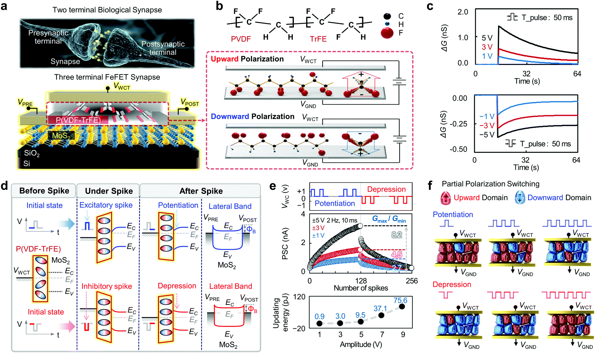 | ||
| Fig. 1 (a) Schematics of biological synapse (upper panel) and three-terminal FeFET synaptic device with P(VDF-TrFE) gate dielectric and MoS2 channel (lower panel). (b) Graphical illustration of polarization switching mechanism in the P(VDF-TrFE). (c) PSC responses triggered by positive (upper panel) and negative (lower panel) VWC spikes with three different amplitudes of 1, 3, 5 V and td of 10 ms. (d) Vertical and lateral energy-band diagrams before and after potentiation (top) and depression (bottom) pulses. (e) PSC values as applying three kinds of pulse sets with different amplitudes of ±1, ±3, ±5 V (upper panel). Updating energy for different amplitudes of the voltage pulses (lower panel). (f) Graphical illustration of partial polarization switching by potentiation and depression pulses. | ||
As shown in the lower panel of Fig. 1b, the application of negative voltage to the WCT causes the dipoles in the PVDF film to orientate in the direction normal to the surface of the film as a result of alignment with the applied electric field (E-field). This orientation of the dipoles is maintained even after removal of the external electric field, resulting in a nonvolatile memory characteristic. In contrast, the opposite polarization occurs under positive voltage bias conditions (downward polarization). To determine whether this polarization mechanism enables the operation of the synaptic device, we investigated the change in conductance for various pulses, as shown in Fig. 1c. Nonvolatile responses were observed for various input spiking pulses with amplitudes of ±1, ±3, ±5 V, and time duration (td) of 10 ms. The percentage of the “conductance remaining after 64 s” relative to the “initial conductance value immediately after pulse application” is 8%, 26%, and 29% for exhibitory (positive) pulses with amplitudes of 1, 3, and 5 V, and 33%, 62%, and 71% for inhibitory (negative) pulses with amplitudes of −1, −3, and −5 V, respectively. Further details on conductance decay phenomenon as a function of pulse width are provided in the ESI,† Fig. S1. The potentiation (by an excitatory pulse, top) and depression (by an inhibitory pulse, bottom) responses were explained with the energy-band diagrams for the synaptic device, as shown in Fig. 1d. The application of an exhibitory spike to the WCT caused the energy-band of the MoS2 semiconductor to instantly bend upward and electrons were attracted to the MoS2 channel region. Simultaneously, randomly oriented dipoles in the P(VDF-TrFE) were aligned with the direction of the induced E-field. Consequently, the channel potential increased because of the aligned dipole moment, and the decreased tunneling width at the source-MoS2 junction resulted in higher carrier injection (channel conductance↑ = potentiation). In contrast, the application of an inhibitory spike resulted in the MoS2 energy-band instantly bending downward and the amount of electrons accumulated at the MoS2 channel to decrease. As a result, the channel potential is decreased and the tunneling width at the source-MoS2 junction increases, lowering the carrier injection (channel conductance↓ = depression). As a higher voltage pulse is supplied, molecules in the P(VDF-TrFE) are polarized even more strongly, causing a much larger change in the channel conductance.
Then, as shown in Fig. 1e (upper panel), we measured the postsynaptic current (PSC) by applying three kinds of pulse sets with different amplitudes (±1, ±3, ±5 V) consecutively to evaluate the LTP/D characteristics. Each pulse set consists of 128 excitatory and 128 inhibitory pulses, where the duration and interval of the pulses were fixed at 10 and 490 ms, respectively. The PSC changed gradually according to the excitatory and inhibitory spikes, consequently presenting general LTP/D characteristics. Especially, as the pulse amplitude increased from +1 to +5 V, the increase in the PSC became greater with each pulse to raise the maximum PSC (after 128 excitatory pulses) from 0.87 to 2.98 nA. As a result, the DR (Gmax/Gmin) was increased from 2.7 (for a 1 V pulse) to 8.7 (for a 5 V pulse). We also examined the effect of the change in the pulse amplitude in terms of energy consumption for updating, as shown in Fig. 1e (lower panel). The estimated energy was below 9.5 pJ for the pulses that were considered in the aforementioned measurements, and was lower than or comparable to the updating energy of FET-type synapses reported thus far (10 pJ).6,34,35 When increasing the pulse amplitude to 7 and 9 V, the updating energy was raised to 37.1 and 75.6 pJ, respectively. Additional information on the change in the updating energy with respect to the amplitude and duration of the pulses is provided in ESI,† Fig. S2. The gradual change in the conductance of the proposed Fe-FET synapse can be explained by partial polarization switching in the ferroelectric domains, as shown in Fig. 1f.22,24 When an excitatory spike is applied, the polarization domains in the P(VDF-TrFE) film are influenced by the direction of the induced E-field, which is aligned downward. This change in the polarization domains gradually occurs as the spike pulse is applied consecutively, thereby increasing the number of electrons in the channel region. In contrast, when an inhibitory spike is applied consecutively, the opposite direction of the E-field gradually aligns the polarization domains upward, thereby decreasing the number of electrons in the channel.
Because the P(VDF-TrFE) typically exhibits a thermodynamically stable ferroelectric phase (β-phase) when annealed between the Curie and melting temperatures, the processing temperature for crystallization is an important parameter for the implementation of P(VDF-TrFE)-based synaptic devices.33Fig. 2 presents the results of our investigation of the ferroelectric characteristics of the P(VDF-TrFE) films, which were annealed at four different annealing temperatures (60, 100, 140, and 180 °C) for 2 hours. For the capacitance–voltage analysis in Fig. 2a, we prepared ferroelectric capacitors with a metal-ferroelectric-metal (MFM) structure (area: 1 mm2), where 150 nm-thick Pt, 50 nm-thick Au, and 395 nm-thick P(VDF/TrFE) films were used as the bottom electrode, the top electrode, and the ferroelectric material, respectively. An AC voltage signal with an amplitude of 0.1 V and a frequency of 100 kHz was used for the capacitance measurement. The “butterfly loop” observed in the C–V characteristic curves indicates that ferroelectric properties were successfully conferred upon the corresponding P(VDF/TrFE) films.36 As shown in Fig. 2b (upper panel), this ferroelectric characteristic appeared in all capacitor samples except for the sample annealed at the lowest temperature of 60 °C, i.e., below the Curie temperature; furthermore, the hysteresis window broadened as the temperature increased. The hysteresis window indicates the difference between two coercive voltages, which are defined as external voltage to lower the net polarization of a ferroelectric film to zero.37 Thus, a ferroelectric capacitor with a wide hysteresis window formed at a high temperature means that a larger amount of energy was required to switch the polarization. The capacitance per unit area also increased when the annealing temperature increased to 140 °C, which indicates that the remnant polarization was enhanced in this temperature range as shown in Fig. 2b (lower panel). This increasing trend in switching energy and remnant polarization can be explained by the growing size of the ferroelectric domains shown in Fig. 2c (upper panel).38,39 However, the capacitance per unit area was lowered slightly when the annealing temperature increased from 140 to 180 °C, which could not be simply explained by the ferroelectric domain size because the hysteresis window increased in the same range. This is because certain parts of the β-phase domains responsible for ferroelectricity are transformed to α- and γ-phase domains, which have nonpolar characteristics above the melting temperature (164.7 °C). The creation of α- and γ-phase domains increases the spacing among the β-phase domains and reduces the size of the β-phase domains as graphically illustrated in Fig. 2c (upper panel, 180 °C), consequently increasing the polarization switching energy and decreasing the remnant polarization, respectively. Additionally, polarization-voltage hysteresis loops of each annealing condition are presented in ESI,† Fig. S3. For a reference, as shown in Fig. 2c (lower panel), the molecular dipoles in the β-phase structure are completely aligned in the same direction perpendicular to the long axis of the polymer chain, thereby showing large spontaneous polarization.32 In contrast, the dipoles in α- and γ-phase structures are alternately arranged in opposite directions along the axis of the polymer chain, thereby canceling the polarities of the dipoles vectorially. The Curie and melting temperatures of the P(VDF-TrFE) film were also confirmed to be 88.3 and 164.7 °C, respectively, by differential scanning calorimetry (DSC) analysis in ESI,† Fig. S4.
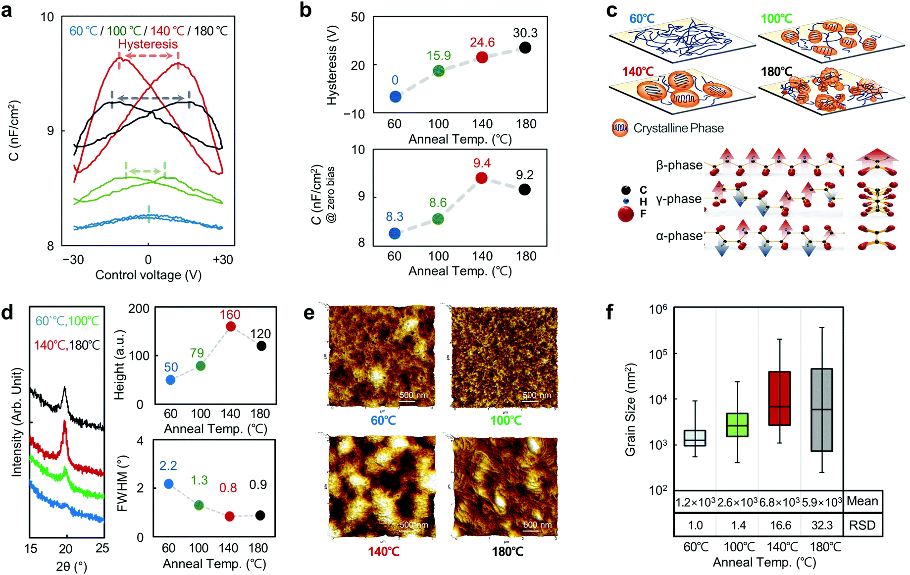 | ||
| Fig. 2 (a) Capacitance–voltage analysis of ferroelectric capacitors with a metal-ferroelectric-metal (MFM) structure. (b) Hysteresis voltage (upper panel) and capacitance per unit area (lower panel) as a function of annealing temperature. (c) Graphical illustration on the changes in crystalline phase with respect to the annealing temperatures, and atomic arrangement of the phase structures of P(VDF-TrFE). (d) X-ray diffraction (XRD) analysis results, (e) atomic force microscopy (AFM) images, and (f) extracted mean (μ) and RSD values of the ferroelectric domain sizes as a function of annealing temperature. | ||
The changes in the ferroelectric domains as a function of the annealing temperature were also confirmed by using X-ray diffraction (XRD) and atomic force microscopy (AFM) analyses, as shown in Fig. 2d and e. In each of the XRD patterns measured for the P(VDF-TrFE) samples annealed at four different temperatures, the peaks related to the β-phase domain were observed near 2θ = 20°.33 As the annealing temperature was increased from 60 to 140 °C (below the melting temperature), we observed a gradual increase in the peak intensity with a corresponding decrease in the full width at half maximum (FWHM) from 2.2 to 0.8°. These changes support the previous prediction that the size of the β-phase domains increased. The decrease in the peak intensity and the slight increase in FWHM that appeared at 180 °C indicate the reduced proportion of the β-phase domain relative to the entire P(VDF-TrFE) film and the decreased size of the β-phase domains, respectively. These changes experimentally support the previous explanation on the basis of the transformation from the β-phase to the α- and γ-phases above the melting temperature. The AFM images of the P(VDF-TrFE) surface also reflect these changes in the ferroelectric domains: (i) below the melting temperature, the β-phase domains continuously grew as the annealing temperature increased and (ii) above the melting temperature, the area occupied by the β-phase diminished because of the formation of additional α- and γ-phases above this temperature (Fig. 2e). To quantitatively evaluate the relationship between the annealing temperature and the size and distribution of ferroelectric domains, we then extracted the mean (μ) and RSD (standard deviation (σ)/mean (μ)) values for the domain sizes from the AFM images (Fig. 2f). The mean and RSD values for the ferroelectric domain sizes increased from 1.2 × 10³ to 6.8 × 10³ nm2 and from 1.0 to 16.6, respectively, as the temperature increased from 60 to 140 °C. At 180 °C, i.e., above the melting point, the mean value decreased by 13.2% (6.8 × 10³ → 5.9 × 10³ nm2) compared with the value at 140 °C, and the RSD value increased by 94.6% (16.6 → 32.3). These changes are different from the changing trend in the mean and RSD values in the temperature range below the melting point. This is because certain parts of β-phase domains are unevenly converted into α- and γ-phases, resulting in a larger size difference among the ferroelectric domains. The ID–VG characteristics of the P(VDF-TrFE) FeFET synapse samples annealed at the four different temperatures and the relevant device performance analysis are provided in ESI,† Fig. S5.
In addition to the characteristics of the ferroelectric layer, the carrier barrier height at the MoS2–metal junction is another important factor that affects the performance of the FeFET synapse. We thus investigated the extent to which different metal contacts on the MoS2 channel influence the operation of the FeFET synapse. Ti, Cr, and Pd contacts, respectively, were applied to the source/drain components of the FeFET synapse, where the P(VDF-TrFE) layer was formed at 140 °C to maximize the size and portion of the β-phase domains. The ID–VG characteristic curves measured for the devices with these three distinct contacts presented different shapes, as shown in the upper left panel of Fig. 3a. This is because the barrier height differed with respect to the metals and consequently the source metals provided a different number of carriers to the MoS2 channel (upper right panel of Fig. 3a). In particular, the different metal contacts affected the levels and ratio of the two current points (at VG = 0 V) that appeared because of the counter-clockwise (CCW) hysteresis resulting from the polarization of the ferroelectric layer. We extracted two conductance (GFeFET) values at VG = 0 from each ID–VG curve and then plotted the values in Fig. 3a (lower panel), where GFS (or GRS) denotes the forward (or reverse) sweep conductance and GRS/GFS means the ratio of the reverse conductance to the forward conductance. Replacement of the Ti contact by Pd lowered the GFS and GRS from 260 and 360 nS (Ti contact) to 0.27 and 3.6 nS (Pd contact), respectively, but the GRS/GFS ratio increased from 1.4 (Ti contact) to 13.0 (Pd contact). This is because of the increase in the barrier height for injecting carriers (for reference, the effective barrier heights for Ti, Cr, and Pd contacts on MoS2 were confirmed experimentally as 50, 80, and 400 meV).40–42 We then applied 128 excitatory and 128 inhibitory spikes (VWC = 5 and −5 V, td = 10 ms, 2 Hz) to investigate the LTP/D characteristics of the three kinds of FeFET synapses. As shown in Fig. 3b, the LTP/D curves were distributed in different current ranges and especially showed that the synaptic properties, such as the DR (GMAX/GMIN), NL, number of effective states, and symmetricity, were affected.
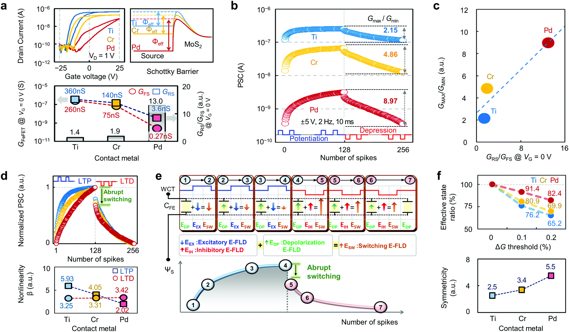 | ||
| Fig. 3 (a) ID–VG characteristic curves of the devices with Ti, Cr, Pd contacts (upper left pannel) and energy-band diagrams of source-MoS2 junctions (upper right pannel). Forward and reverse conductances at VG = 0 with respect to contact metals, and corresponding conductance ratio GFS/GRS (lower panel). (b) PSC responses of the devices with Ti, Cr, Pd contacts induced by 128 excitatory and 128 inhibitory spikes (VWC = ±5 V, td = 10 ms, 2 Hz). (c) Dynamic range as a function of the GRS/GFS ratio. (d) Normalized PSC values and nonlinearity of the devices with Ti, Cr, Pd contacts. (e) Dipole alignment and corresponding surface potential (ΨS) in P(VDF-TrFE) capacitor (CFE) according to the consecutive application of the excitatory and inhibitory pulses. (f) Effective conductance state ratio as a function of ΔG threshold (upper pannel). Symmetricity of PSC responses with respect to contact metals (lower pannel). | ||
The DR was linearly dependent on the GRS/GFS ratio, where the GMAX/GMIN value of the Pd contact device (8.97) was much higher than the values of the Ti and Cr devices (2.15 and 4.86, respectively) owing to the larger GRS/GFS ratio, as shown in Fig. 3c. In addition, the three kinds of contacts affected the NL of the LTP/D characteristic curves. To compare the NL values, we normalized the LTP/D curves with the highest PSC values and then extracted the NL values, as shown in Fig. 3d. In the LTP region, the NL was observed to have improved in the Pd-contacted device (β = 2.02) compared with the Cr and Ti devices (β = 4.05 and 5.93, respectively). In the LTD region, the NL value was independent from the contact metals, and was slightly degraded from 3.25 (Ti) to 3.31 (Cr) and then to 3.42 (Pd). Details on the calculation of NL are provided in ESI,† Fig. S6. The application of excitatory pulses to the WCT in the FeFET synapse resulted in the dipoles in the P(VDF-TrFE) capacitor (CFE) aligning with the direction of the applied E-field, creating a depolarization E-field (EDP) in the direction opposite to the applied excitatory E-field (EEX), as shown in Fig. 3e.39 Because the EDP is negligible in the initial part of the LTP region, the EEX mostly contributes to the dipole switching E-field (ESW), resulting in a sufficient increase in the surface potential (ΨS) (stage 1 → 2). However, continued application of the excitatory pulses causes the EDP to increase such that it suppresses the dipole switching ability of the applied pulses. This consequently reduces the extent to which ΨS increases (stage 2 → 3 → 4), as shown in Fig. 3e (lower left panel). Owing to this decrease in the rate whereby ΨS increases, upward-bending LTP curves were observed in all of the FeFET synapses. Especially, for the devices with low barrier contact metals such as Ti and Cr, the upward-bending behavior appeared to be more severe. This is because the direct and/or Fowler–Nordheim (F–N) tunneling mechanism contributes to the increase in the PSC and the tunneling current is expected to dominate the thermionic current.43 In the case of the Pd-contacted device with its relatively high injection barrier, the upward-bending phenomenon was much less pronounced than the other devices because the thermionic emission mechanism is expected to contribute to the increase in the PSC dominantly.44 The application of inhibitory pulses to the P(VDF-TrFE) capacitor (CFE) with maximized depolarization results in an external inhibitory field (EIH) with the same direction as the EDP, instantly inducing the largest ESW to the ferroelectric capacitor. This has the effect of abrupt dipole switching in the ΨS curve, as shown in the lower right panel of Fig. 3e (stage 4 → 5). Immediately after the application of the first inhibitory pulse, because of the large residual EDP that still remains, the ΨS is predicted to decrease considerably (stage 5 → 6). Finally, the extent to which the ΨS decreases with respect to the subsequent inhibitory pulses is lowered because of the continuous decrease in the EDP (stage 6 → 7). Consequently, downward-bending LTD curves are observed in all of the FeFET synapses. The LTD characteristic curves of the low barrier metal-contacted devices (Ti, Cr) were bent similarly to that of the high barrier metal-contacted devices (Pd), resulting in analogous nonlinearities. We then investigated the effective conductance-state ratios with respect to the contact metals (Fig. 3f (upper panel)). The effective conductance-state ratio was defined as the ratio of the number of conductance states in which ΔG exceeded a certain percentage of Gmax/Gmin to the total number of conductance states (Fig. S7, ESI†). That is, insufficient conductance changes (ΔG) that do not affect the recognition rate were excluded. The effective conductance-state ratios of all of the FeFET synapses decreased as the ΔG threshold increased. The ratio of the Pd-contacted device was maintained at 82.4% even when ΔG increased to 0.2% because of its excellent linearity, whereas those of the Ti and Cr-contacted devices were as low as 65.2% and 69.9%, respectively. In addition, the symmetricity between the LTP and LTD curves was investigated with respect to the contact metals, as shown in Fig. 3f (lower panel). The method that was used to estimate the symmetricity is provided in ESI,† Fig. S8. The symmetricity value of the Pd-contacted device (5.5) was much higher than those of the Ti- and Cr-contacted devices (2.5 and 3.4, respectively) owing to the enhanced linearity in the LTP region. Overall, the synaptic performance of the Pd-contacted device was superior to that of the Ti- and Cr-contacted devices in terms of the DR, NL, effective conductance-state ratio, and symmetricity.
In an attempt to understand the way in which these synaptic characteristics affect the training and inferencing tasks of the multi-layer perceptron NNs (ML-NNs) composed of the FeFET synapses, we used the synaptic characteristics to construct an ML-NN and then conducted training/inferencing simulation with the MNIST fashion dataset, as shown in Fig. 4a.13,45 Our dataset included 10 categories of fashion items and consisted of a training set of 60![[thin space (1/6-em)]](https://www.rsc.org/images/entities/char_2009.gif) 000 example images and a test set of 10000 example images. A fashion MNIST image has 28 × 28 pixels, of which the grayscale values range from 0 to 255.46 As shown in Fig. 4b, the ML-NN consisted of one input layer (IL), one hidden layer (HL), and one output layer (OL), where the layers were composed of 784 input neurons, 100 hidden neurons, and 10 output neurons, respectively. Additionally, each neuron in one layer was connected to every neuron in the next layer via the FeFET synapses. The weight of the FeFET synapse used to connect the i-th neuron in the IL with the h-th neuron in the HL was indicated as WIHi,h. Similarly, the weight of the synapse between the h-th neuron in the HL and o-th neuron in the OL was WHOh,o. The 128 conductance states were normalized by the maximum state value and the normalized conductance values were used as the synaptic weights. The training process consisted of two key operations: feed-forward (FF) and backpropagation (BP). In the FF operation, 784 input voltage signals (VILi for the i-th signal in the IL) with values between 0 and 1 were obtained from the 28 × 28 pixels of the fashion images, and those input signals were applied to the corresponding input neurons. They were consequently transformed to 100 weighted sum currents (
000 example images and a test set of 10000 example images. A fashion MNIST image has 28 × 28 pixels, of which the grayscale values range from 0 to 255.46 As shown in Fig. 4b, the ML-NN consisted of one input layer (IL), one hidden layer (HL), and one output layer (OL), where the layers were composed of 784 input neurons, 100 hidden neurons, and 10 output neurons, respectively. Additionally, each neuron in one layer was connected to every neuron in the next layer via the FeFET synapses. The weight of the FeFET synapse used to connect the i-th neuron in the IL with the h-th neuron in the HL was indicated as WIHi,h. Similarly, the weight of the synapse between the h-th neuron in the HL and o-th neuron in the OL was WHOh,o. The 128 conductance states were normalized by the maximum state value and the normalized conductance values were used as the synaptic weights. The training process consisted of two key operations: feed-forward (FF) and backpropagation (BP). In the FF operation, 784 input voltage signals (VILi for the i-th signal in the IL) with values between 0 and 1 were obtained from the 28 × 28 pixels of the fashion images, and those input signals were applied to the corresponding input neurons. They were consequently transformed to 100 weighted sum currents (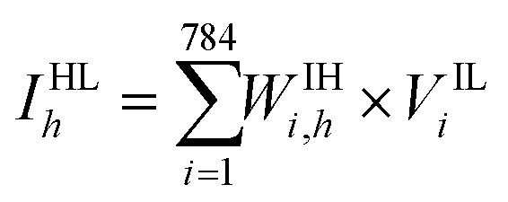 for the h-th current in the HL). After that, the 100 hidden voltage signals (VHLh = f(IHLh) for the h-th signal in the HL) were obtained via the sigmoid activation function
 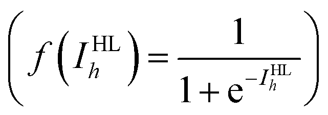 . The hidden signals were then converted to 10 output voltage signals by the weighted sum operation (
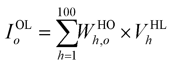 for the o-th current in the OL) and the sigmoid activation function (
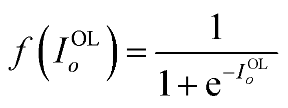 ). Finally, the 10 output signals (VOLo for the o-th signal in the OL) were compared with each label value (Ko) to calculate the error (Eo = Ko − VOLo). In the BP operation, the errors propagated backward from the OL to the IL, subsequently updating the synaptic weights in a propagating way by minimizing the errors by the adaptive moment estimation (ADAM) algorithm.47 For a reference, we modified the distribution of the synaptic weights such that they were between −1 and 1 by using the following equation, WMOD = 2 × W − 1.
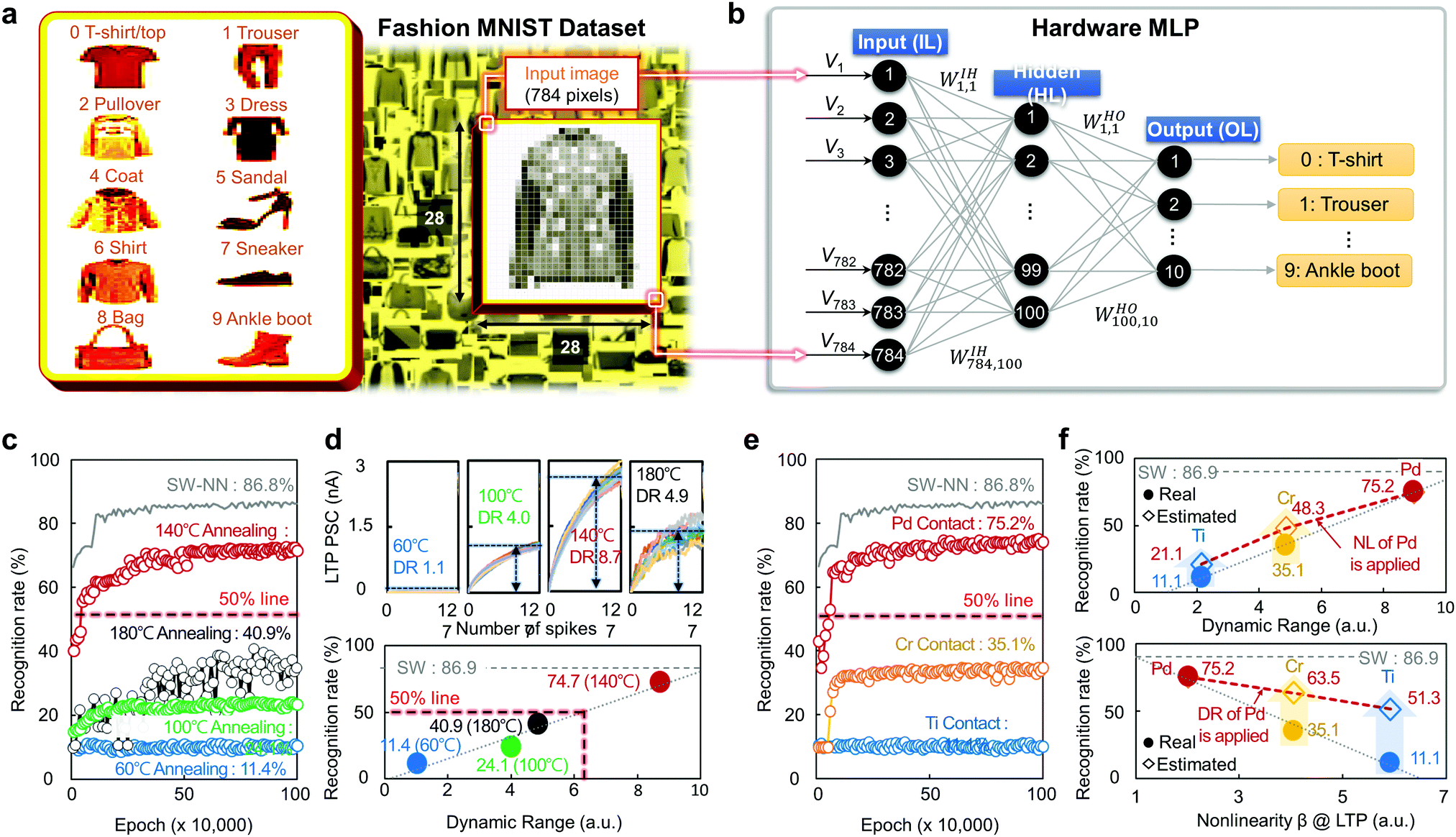 | ||
| Fig. 4 (a) Schematic illustrations of MNIST fashion dataset and (b) constructed ML-NN. (c) Recognition rate as a function of the number of epochs with respect to annealing temperatures for P(VDF-TrFE) film. (d) LTP PSC responses as a function of the number of spikes (upper panel). Recognition rate according to the corresponding DR (lower panel). (e) Recognition rate as a function of the number of epochs with respect to contact metals. (f) Recognition rate as functions of DR (upper panel) and LTP nonlinearity (lower panel). | ||
We then trained the ML-NN with the 60000 training images from the MNIST fashion dataset and extracted the recognition rates after every 10000 training step (1 epoch) with the 10000 images in the testing dataset. The left panel of Fig. 4c shows the recognition rate as a function of the number of epochs with respect to the annealing temperature for the P(VDF-TrFE) film. After sufficient training over 50 epochs, the ML-NN constructed with FeFET synapses annealed at 140 °C demonstrated a high recognition rate of 74.7%, which is slightly lower than that of the SW-NN (86.8%). In comparison, the recognition rates of the other ML-NNs did not even reach 50% (11.4%, 24.1%, and 40.9% for the FeFET synapses annealed at 60 °C, 100 °C, and 180 °C, respectively). This is because the relatively superior ferroelectric characteristics of the P(VDF-TrFE) layer annealed at 140 °C enabled synaptic operation in a wider DR. As evidence thereof, we confirmed the highest DR value of 8.7 in the 140 °C FeFET synapse sample after ten LTP characteristic measurements (Fig. 4d). The FeFET synapse based on the P(VDF-TrFE) annealed at 180 °C underwent considerable fluctuation at the PSC level and in its recognition rate. This is considered to be caused by the large variation in the size of the ferroelectric domains (see Fig. 2). We then plotted the maximum recognition rate according to the corresponding DR in Fig. 4d (lower panel), where we confirmed that a DR greater than 6.3 is required to achieve a recognition rate of over 50% in the proposed ML-NN. Similarly, the recognition rates of the ML-NN based on the FeFET synapses annealed at 140 °C were investigated to examine the effect of the contact metal (Fig. 4e). The maximum recognition rate for the Pd-contacted synapse was approximately 75.2%, which was slightly lower than that of the SW-NN (86.8%). However, the rates of the NNs formed by the Ti- and Cr-contacted synapses were 11.1% and 35.1% because of their lower DR and NLLTP (2.15 and 5.93 for the Ti-synapse; 4.86 and 4.05 for the Cr-synapse). In comparison, the corresponding values for the Pd-synapse device were 8.97 (DR) and 2.02 (NLLTP). We then conducted additional simulations with ML-NNs to examine the effects of the DR and NL on the recognition rate independently (Fig. 4f): (i) the NL of the Pd-synapse was applied to the other Ti-/Cr-synapses (upper panel). (ii) The DR of the Pd-synapse was used for the Ti-/Cr-synapses (lower panel). As shown in Fig. 4f (upper panel), the recognition rates for the Ti- and Cr-synapses increased slightly owing to the improved NL value; the rates increased by 10.0%p and 13.2%p, respectively. When the DR of the Pd-synapse was used for all of the synapses, the recognition rates were enhanced more markedly from 11.1 to 51.3% (40.2%p) and from 35.1 to 63.5% (28.4%p) for the Ti- and Cr-synapses, respectively. Additional simulation results are provided in ESI,† Fig. S9. Overall, we could confirm that the influence of the DR on the recognition rate of the ML-NNs we used was greater than that of the NL. In addition, we conducted simulations on ML-NNs using MNIST handwritten digits dataset as shown in ESI,† Fig. S10. The maximum recognition rate for the Pd-contacted synapse was 92.1%.
Conclusions
In summary, we demonstrated a polymer-based FeFET synaptic device by using P(VDF-TrFE) ferroelectric and MoS2 semiconducting materials with a very small number of surface defects to successfully mimic the operation of a biological synapse. The excellent ferroelectric properties (CFE = 9.4 nF cm−2) of the P(VDF-TrFE) film were achieved by optimizing the annealing conditions (140 °C, 2 hours), which maximized the size and portion of the β-phase domains (mean grain size = 6.8 × 10³, RSD = 16.6). The effects of the contact barrier height on the synapse performance were also studied thoroughly. The Pd-contacted device, of which the barrier was higher than those of the Ti- and Cr-contacted devices, had a wider DR (8.97) owing to the larger GRS/GFS ratio (13.0) and higher NL (βLTP = 2.02 and βLTD = 3.42). This was attributed to the relatively gradual conductance change that was possible because the carrier injection only depended on the thermionic emission mechanism. In addition, the superior effective conductance-state ratio (82.4% at ΔGThreshold of 0.2%) and symmetricity (5.5) of the Pd-contacted device were the result of the improvements in DR and NL. We then constructed the ML-NNs with the synaptic characteristics and performed the training/inferencing simulation with the MNIST fashion dataset. The recognition rates of the ML-NNs consisting of the synapses annealed at 60, 100, and 180 °C did not exceed 50%, whereas the ML-NN composed of the synapses annealed at 140 °C had a higher recognition rate of 74.7%. This was because the enhanced ferroelectricity of the P(VDF-TrFE) film annealed at 140 °C enabled a wider DR. The experiment we conducted to determine the effect of the contact metal on the recognition rate revealed that the maximum recognition rate by the Pd-contact synapses was approximately 75.2%. This was slightly lower than that of SW-NN (86.8%), whereas the rates obtained with the other metal-contacted synapses were less than 50%. Overall, a wide DR was found to be the most essential factor to achieve a high recognition rate in the proposed ML-NNs with the FeFET synapses. We expect the optimizations of ferroelectric and contact-metal materials and the relevant studies performed with the proposed polymer-based FeFET synaptic device to be a cornerstone for the development of high-performance synaptic devices in future.Experimental
Fabrication of MFM capacitor
A patterned bottom electrode consisting of Ti/Pt (10/150 nm) layers was formed via thermal deposition on a Si wafer with a 90 nm-thick thermally grown SiO2 gate dielectric layer. P(VDF-TrFE) 80:20 mol% copolymer powder was dissolved in the solvent methyl-ethyl-ketone (MEK) in a 5 wt% ratio. Then, a P(VDF-TrFE) layer was spin-coated on the bottom electrode at 1500 rpm for 30 s under ambient atmospheric conditions. The thickness of P(VDF-TrFE) was confirmed as 394.8 nm by vertical scanning electron microscopy (V-SEM). Each film was then annealed at 60 °C, 100 °C, 140 °C, or 180 °C for 2 h to evaporate the MEK and to study the effects of the annealing temperature on the ferroelectricity. Finally, a top electrode (thickness: 50 nm) was formed by evaporating Au through a shadow mask on top of the P(VDF-TrFE) layers. The width and length of the ferroelectric capacitors were 1 × 1 mm, respectively. Cross-view SEM and top-view SEM images with respect to the annealing temperatures are provided in ESI,† Fig. S11.
Fabrication of FeFET synaptic device
A MoS2 flake was mechanically exfoliated and transferred onto the 90 nm-thick SiO2 layer on the Si substrate (doped intensively with boron) via adhesive tape (224SPV, Nitto). Source and drain electrodes with spacing of 5 μm were patterned on the MoS2 samples by an optical lithography process, followed by Ti/Au (10/40 nm), Cr/Au (10/40 nm), and Pd/Au (10/40 nm) deposition via an e-beam evaporator. Then, the P(VDF-TrFE) layers were spin-coated at 1500 rpm for 30 s and then annealed at various temperatures. Subsequently, a Pd/Au (10/40 nm) top gate electrode (15 μm wide) was formed on top of the P(VDF-TrFE) layers by an optical lithography process and an e-beam evaporator.Characterization of FeFET synaptic device
The electrical characteristics of the FeFET synapses were measured using a Keysight B2912 measurement unit connected to a Keysight 33500B waveform generator unit at room temperature. The capacitances of the MFM capacitors were investigated using an Agilent E4980A precision LCR meter. The β-phase peaks of the P(VDF-TrFE) were analyzed with a Bruker D8-ADVANCE instrument, and the surface morphologies of the P(VDF-TrFE) were inspected via tapping-mode AFM (Asylum Cypher S AFM system).Conflicts of interest
There are no conflicts to declare.Acknowledgements
This research was supported by the Basic Science Research Program, Basic Research Lab Program, and Nano-Material Technology Development Program through National Research Foundation of Korea (NRF) grants funded by the Korean government (MSIP) (2020R1A4A2002806, 2019M3F3A1A01074451, 2018R1A2A2A05020475, and 2016M3A7B4910426), and the Future Semiconductor Device Technology Development Program (10067739) funded by the Ministry of Trade, Industry and Energy (MOTIE), and the Korean Semiconductor Research Consortium (KSRC). This work was supported by Samsung Electronics Co., Ltd (IO201210-07994-01)Notes and references
- E. J. Fuller, S. T. Keene, A. Melianas, Z. Wang, S. Agarwal, Y. Li, Y. Tuchman, C. D. James, M. J. Marinella and J. J. Yang, Science, 2019, 364, 570–574 CrossRef CAS.
- Y. LeCun, Y. Bengio and G. Hinton, Nature, 2015, 521, 436–444 CrossRef CAS.
- Q. Xia and J. J. Yang, Nat. Mater., 2019, 18, 309–323 CrossRef CAS.
- D. Ielmini and H.-S. P. Wong, Nat. Electron., 2018, 1, 333–343 CrossRef.
- K. Roy, A. Jaiswal and P. Panda, Nature, 2019, 575, 607–617 CrossRef CAS.
- Y. van de Burgt, E. Lubberman, E. J. Fuller, S. T. Keene, G. C. Faria, S. Agarwal, M. J. Marinella, A. A. Talin and A. Salleo, Nat. Mater., 2017, 16, 414–418 CrossRef CAS.
- P. S. Churchland and T. J. Sejnowski, The computational brain, MIT Press, 2016 Search PubMed.
- C. Mead, Proc. IEEE, 1990, 78, 1629–1636 CrossRef.
- C. Wan, P. Cai, M. Wang, Y. Qian, W. Huang and X. Chen, Adv. Mater., 2020, 32, 1902434 CrossRef CAS.
- P. A. Merolla, J. V. Arthur, R. Alvarez-Icaza, A. S. Cassidy, J. Sawada, F. Akopyan, B. L. Jackson, N. Imam, C. Guo and Y. Nakamura, Science, 2014, 345, 668–673 CrossRef CAS.
- G. W. Burr, R. M. Shelby, S. Sidler, C. Di Nolfo, J. Jang, I. Boybat, R. S. Shenoy, P. Narayanan, K. Virwani and E. U. Giacometti, IEEE Trans. Electron Devices, 2015, 62, 3498–3507 Search PubMed.
- D. H. Kang, J. H. Kim, S. Oh, H. Y. Park, S. R. Dugasani, B. S. Kang, C. Choi, R. Choi, S. Lee and J.-H. Park, Adv. Sci., 2019, 6, 1901265 CrossRef.
- M.-K. Kim and J.-S. Lee, Nano Lett., 2019, 19, 2044–2050 CrossRef CAS.
- M. Prezioso, F. Merrikh-Bayat, B. Hoskins, G. C. Adam, K. K. Likharev and D. B. Strukov, Nature, 2015, 521, 61–64 CrossRef CAS.
- J. Sun, S. Oh, Y. Choi, S. Seo, M. J. Oh, M. Lee, W. B. Lee, P. J. Yoo, J. H. Cho and J.-H. Park, Adv. Funct. Mater., 2018, 28, 1804397 CrossRef.
- H.-S. P. Wong, S. Raoux, S. Kim, J. Liang, J. P. Reifenberg, B. Rajendran, M. Asheghi and K. E. Goodson, Proc. IEEE, 2010, 98, 2201–2227 Search PubMed.
- S. Yu, Y. Wu, R. Jeyasingh, D. Kuzum and H.-S. P. Wong, IEEE Trans. Electron Devices, 2011, 58, 2729–2737 CAS.
- S. Seo, S. H. Jo, S. Kim, J. Shim, S. Oh, J. H. Kim, K. Heo, J. W. Choi, C. Choi, S. Oh, D. Kuzum, H. P. Wong and J.-H. Park, Nat. Commun., 2018, 9, 5106 CrossRef.
- Y. Nishitani, Y. Kaneko, M. Ueda, T. Morie and E. Fujii, J. Appl. Phys., 2012, 111, 124108 CrossRef.
- Z. Yin, B. Tian, Q. Zhu and C. Duan, Polymers, 2019, 11, 2033 CrossRef CAS.
- S. Jang, S. Jang, E.-H. Lee, M. Kang, G. Wang and T.-W. Kim, ACS Appl. Mater. Interfaces, 2018, 11, 1071–1080 CrossRef.
- M. Jerry, S. Dutta, A. Kazemi, K. Ni, J. Zhang, P.-Y. Chen, P. Sharma, S. Yu, X. S. Hu and M. Niemier, J. Phys. D: Appl. Phys., 2018, 51, 434001 CrossRef.
- S. Oh, T. Kim, M. Kwak, J. Song, J. Woo, S. Jeon, I. K. Yoo and H. Hwang, IEEE Electron Device Lett., 2017, 38, 732–735 CAS.
- M. Jerry, P.-Y. Chen, J. Zhang, P. Sharma, K. Ni, S. Yu and S. Datta, IEEE Int. Electron Devices Meet., 2017, 6.2.1–6.2.4 Search PubMed.
- X. Sun, P. Wang, K. Ni, S. Datta and S. Yu, IEEE Int. Electron Devices Meet., 2018, 3.1.1–3.1.4 Search PubMed.
- E. Tansey, Brain Res. Bull., 1997, 44, 211–212 CrossRef CAS.
- K. Cho, J. Pak, S. Chung and T. Lee, ACS Nano, 2019, 13, 9713–9734 CrossRef CAS.
- A. K. Geim and I. V. Grigorieva, Nature, 2013, 499, 419–425 CrossRef CAS.
- K. Novoselov, A. Mishchenko, A. Carvalho and A. C. Neto, Science, 2016, 353, 6298 CrossRef.
- S. Kim, B. Choi, M. Lim, J. Yoon, J. Lee, H.-D. Kim and S.-J. Choi, ACS Nano, 2017, 11, 2814–2822 CrossRef CAS.
- H. Tian, Q. Guo, Y. Xie, H. Zhao, C. Li, J. J. Cha, F. Xia and H. Wang, Adv. Mater., 2016, 28, 4991–4997 CrossRef CAS.
- T. Furukawa, Phase Transitions, 1989, 18, 143–211 CrossRef CAS.
- D. Mao, B. E. Gnade and M. A. Quevedo-Lopez, Ferroelectr.: Phys. Eff., 2011, 78–100 Search PubMed.
- F. Alibart, S. Pleutin, D. Guérin, C. Novembre, S. Lenfant, K. Lmimouni, C. Gamrat and D. Vuillaume, Adv. Funct. Mater., 2010, 20, 330–337 CrossRef CAS.
- Q. Lai, L. Zhang, Z. Li, W. F. Stickle, R. S. Williams and Y. Chen, Adv. Mater., 2010, 22, 2448–2453 CrossRef CAS.
- T. Furukawa, S. Kanai, A. Okada, Y. Takahashi and R. Yamamoto, J. Appl. Phys., 2009, 105, 061636 CrossRef.
- T. Schenk, E. Yurchuk, S. Mueller, U. Schroeder, S. Starschich, U. Böttger and T. Mikolajick, Appl. Phys. Rev., 2014, 1, 041103 Search PubMed.
- Y. Kim, Y. Cho, S. Hong, S. Bühlmann, H. Park, D.-K. Min, S.-H. Kim and K. No, Appl. Phys. Lett., 2006, 89, 162907 CrossRef.
- L. Yang, X. Li, E. Allahyarov, P. L. Taylor, Q. Zhang and L. Zhu, Polymer, 2013, 54, 1709–1728 CrossRef CAS.
- S. Das, H.-Y. Chen, A. V. Penumatcha and J. Appenzeller, Nano Lett., 2013, 13, 100–105 CrossRef CAS.
- Y. Liu, H. Wu, H. C. Cheng, S. Yang, E. Zhu, Q. He, M. Ding, D. Li, J. Guo and N. O. Weiss, 2014, arXiv preprint arXiv:1412.7718.
- K. Sano, T. Takahashi and K. Uchida, Jpn. J. Appl. Phys., 2016, 55, 036501 CrossRef.
- D. S. Schulman, A. J. Arnold and S. Das, Chem. Soc. Rev., 2018, 47, 3037–3058 RSC.
- S. Lee and A. Nathan, Science, 2016, 354, 302–304 CrossRef CAS.
- P.-Y. Chen, X. Peng and S. Yu, IEEE Int. Electron Devices Meet., 2017, 6.1.1–6.1.4 Search PubMed.
- H. Xiao, K. Rasul and R. Vollgraf, 2017, arXiv preprint arXiv:1708.07747.
- D. P. Kingma and J. Ba, 2014, arXiv preprint arXiv:1412.6980.
Footnotes |
| † Electronic supplementary information (ESI) available. See DOI: 10.1039/d0nh00559b |
| ‡ These authors contributed equally to this work. |
| This journal is © The Royal Society of Chemistry 2021 |