
 Open Access Article
 This Open Access Article is licensed under a
 Creative Commons Attribution 3.0 Unported Licence
Technology progress on quantum dot light-emitting diodes for next-generation displays
Sang Yun
Bang†
 ,
Yo-Han
Suh†
,
Xiang-Bing
Fan
,
Dong-Wook
Shin
,
Sanghyo
Lee
,
Hyung Woo
Choi
,
Tae Hoon
Lee
,
Jiajie
Yang
,
Shijie
Zhan
,
William
Harden-Chaters
,
Chatura
Samarakoon
,
Luigi G.
Occhipinti
,
Soo Deok
Han
*,
Sung-Min
Jung
* and
Jong Min
Kim
,
Yo-Han
Suh†
,
Xiang-Bing
Fan
,
Dong-Wook
Shin
,
Sanghyo
Lee
,
Hyung Woo
Choi
,
Tae Hoon
Lee
,
Jiajie
Yang
,
Shijie
Zhan
,
William
Harden-Chaters
,
Chatura
Samarakoon
,
Luigi G.
Occhipinti
,
Soo Deok
Han
*,
Sung-Min
Jung
* and
Jong Min
Kim
Electrical Engineering Division, Department of Engineering, University of Cambridge, 9 JJ Thomson Avenue, Cambridge, CB3 0FA, UK. E-mail: sh977@cam.ac.uk; sj569@cam.ac.uk
First published on 8th December 2020
Abstract
Quantum dot light-emitting diodes (QD-LEDs) are widely recognised as great alternatives to organic light-emitting diodes (OLEDs) due to their enhanced performances. This focus article surveys the current progress on the state-of-the-art QD-LED technology including material synthesis, device optimization and innovative fabrication processes. A discussion on the material synthesis of core nanocrystals, shell layers and surface-binding ligands is presented for high photoluminescence quantum yield (PLQY) quantum dots (QDs) using heavy-metal free materials. The operational principles of several types of QD-LED device architectures are also covered, and the recent evolution of device engineering technologies is investigated. By exploring the fabrication process for pixel-patterning of QD-LEDs on an active-matrix backplane for full-colour display applications, we anticipate further improvement in device performance for the commercialisation of next-generation displays.
Introduction
Over the past decade, organic light-emitting diodes (OLEDs) have been successfully launched in the display industry, dominating the flat panel display (FPD) market owing to the advantages of self-emissive devices including both performance and form factor metrics, such as high contrast ratio (CR) and substrate flexibility.1,2 However, despite the successful industrialisation of OLEDs, the demand for higher colour saturation and higher electrical stability has emerged for next-generation displays.3 Quantum dots (QDs) are promising materials for the emissive component of self-emissive light-emitting diodes (LEDs) due to their high colour saturation in a narrow wavelength range, easy colour tunability by control of their size and prominent stability.4,5 Particularly, electroluminescence (EL)-based quantum dot light-emitting diodes (QD-LEDs) driven by an electric field also have a flexible form factor and superior CR because they are self-emissive devices such as OLEDs.6,7 Moreover, since EL-based QD-LEDs utilize the ultimate material properties of inorganic QDs, a high colour gamut with high colour tunability and electrical stability are expected.8–10 Therefore, QD-LED technology is getting increasingly attractive as new device technology for next-generation smart displays.To date, the device performances of QD-LEDs such as their external quantum efficiency (EQE), brightness, and lifetime have improved rapidly by developing new QD materials, optimising device architectures and innovating fabrication processes. There have been tremendous efforts to achieve high EQEs, high colour purity and long lifetimes in QD-LED devices. Fig. 1 outlines the three major categories in the development of EL-based QD-LED devices having high electro-optical performances and long lifetimes. In terms of the material, the properties of QD materials, specifically their photoluminescence quantum yield (PLQY), are coupled to the EQE of the QD-LED device, while the uniformity of the core size of QDs gives high colour purity to QD-LEDs. Besides, the material stability is directly related to the lifetime of QD-LEDs. In the case of the device architecture, the transport layers with respect to the QDs are optimised to balance charge injection for both high EQEs and long lifetime. In terms of the fabrication process, the successful patterning technology of red, green and blue pixels with QDs on the active-matrix backplane is crucial to achieve successful mass production of full-colour displays based on QD-LEDs with excellent device performances.
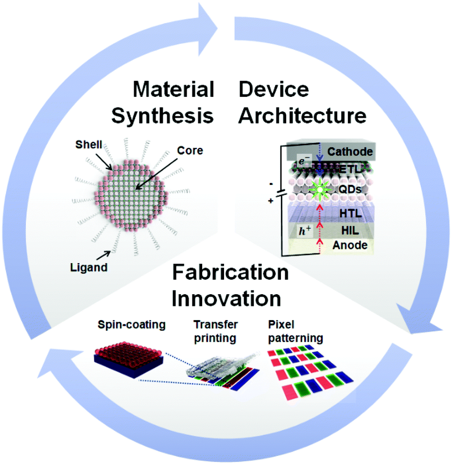 | ||
| Fig. 1 Classification of the development categories for QD-LEDs. Performances of QD-LEDs can be elevated by the combination of technology for QD material synthesis, device optimisation and fabrication process. | ||
This article reviews the fundamental concepts of QD-LEDs and the current progress in the development of QD materials, optimised device architectures and innovative fabrication processes. Firstly, the basic structure of QDs, which includes their core, shell, and ligands, and their functions are explained together with the recent research highlights for high PLQY. Next, the operational principle of QD-LED devices, the different device architectures and the state-of-the-art device engineering technologies of QD-LEDs are discussed. Finally, the evolution of fabrication technology from the solution process to precise patterning process is summarised.
Synthesis of QD materials
A colloidal QD is composed of three parts, as shown in Fig. 2(a): (i) a core nanocrystal, (ii) a shell layer and (iii) a surface-binding ligand.11,12 The core nanocrystal generates light through the radiative recombination of an exciton, which is an electron–hole pair (EHP), confined in the core region.5 The wavelength of the emissive light is determined by the optical bandgap, which is directly modified by the composition and the size of the core nanocrystals. To obtain the desired colour and high colour purity, control of the size and uniformity of the core nanocrystal is the key factor during the synthesis of QDs. As core nanocrystal materials, cadmium selenide (CdSe), indium phosphide (InP) and zinc telluride selenide (ZnTeSe) are commonly used. In contrast to the core nanocrystal, the shell layer gives a quantum confinement effect by surrounding the core.13 The highest occupied molecular orbital (HOMO) of the shell is higher, and the lowest unoccupied molecular orbital (LUMO) of the shell is lower than that of the core, forming a quantum well to confine the exciton within the core nanocrystal.14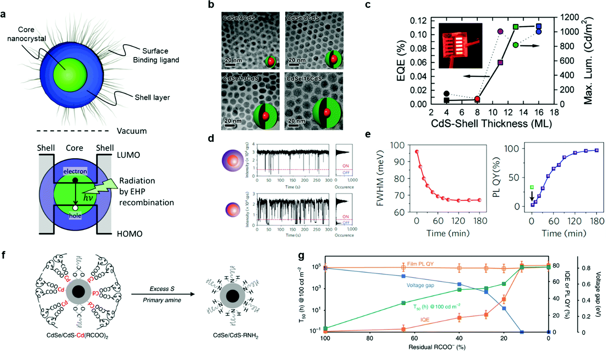 | ||
| Fig. 2 (a) Schematic illustration of a colloidal QD and its energy diagram. (b) Transmission electron microscopy (TEM) images of CdSe/xCdS QDs with various shell thicknesses of 4, 8, 13, and 16 CdS MLs. (c) External quantum efficiency and luminance characteristics of red QD-LEDs as a function of CdS shell thickness (MLs). Copyright 2015, the American Chemical Society. (d) Representative PL blinking race of single CdSe/CdS core–shell QD. Top: Core 2.2 nm/Shell 2.4 nm and Bottom: Core 2.2 nm/Shell 0.7 nm. (e) FWHM of the PL peak of the CdSe/CdS core–shell and PLQY at CdSe Core 5.4 nm. Copyright 2013, Nature Publishing Group. (f) Electrochemically stable ligand exchange from cadmium-carboxylate to primary amines. (g) PLQY of the QD films, IQE of the QLEDs, operational lifetime of the QLEDs, and voltage gap of the QLEDs as a function of the residual percentage of carboxylate ligands. Copyright 2020 Nature Publishing Group. | ||
Typically, the choice of materials for the shell layer is: (i) cadmium sulphide (CdS) or zinc sulphide (ZnS) for CdSe-based QDs, (ii) zinc selenide sulphide (ZnSeS) as a gradient shell for InP-based QDs, and (iii) ZnS for ZnTeSe-based QDs. After the synthesis of the core/shell nanocrystals, it is essential to passivate the shell layer by a surface-binding ligand.15 This ligand covers the defects or the surface ions on the shell so that it protects the QD nanoparticle (NP) from oxygen and moistures. In addition to preventing environmental degradation, the surface-binding ligand increases the colloidal stability by inhibiting the aggregation of QDs in the selective solvent.16 Oleic acid and oleylamine are commonly used as the surface-binding ligand.
Significant progress has been made to develop complex QDs possessing a high PLQY, uniform size distribution and stability. Particularly, since the core of the QDs is degraded by reaction with oxygen and water and other causes such as heat and UV light, it is necessary to protect the QD core from reactive molecules to increase the stability of QDs.17 The device lifetime of QD-LEDs is directly affected by the stability of the QDs, where the device can be expected to have a long lifetime by increasing the stability of the QD materials. One pathway to improving the device lifetime is to optimise the material and the structure of the shell and the ligand of QDs in order to protect the QD core. Therefore, together with optimisation of the core, modification of the shell thickness and minimisation of the lattice mismatch between the core and shell have been proven to be successful routes for achieving a high PLQY and long lifetime by preventing the surface oxidation of the core nanocrystal.15,18 Depending on the length of the surface-binding ligand, there is a trade-off between the colloidal stability in solution and the charge injection in the QD-LED device.19,20 Therefore, it is necessary to carefully choose the surface-binding ligand during the synthesis of QDs. The current progress in various QDs for QD-LEDs, with special attention on their shell layer and surface-binding ligand, is summarised in this section, with notable research on heavy-metal free QDs for full-colour displays.
As a platform material, Cd-based QDs have been widely used to achieve enhanced material properties together with the engineered shell and surface-binding ligand.11,13,14,18,19,21,22 Pal et al. observed the effect of shell thickness on device performance, as shown in Fig. 2(b) and (c).23 The device performance changes corresponded to the thickness of the CdS shell surrounding the CdSe core of the QDs. The EQE and the maximum luminance were measured according to the number of monolayers (MLs) in the shell layer. As result of their systematic study, the highest EQE was achieved for 13 MLs of CdS shell layer with the maximum luminance of over 1000 cd m−2 at a low turn-on voltage of around 3.0 V.
Chen et al. presented a unique synthetic method to grow a shell layer for suppressing the blinking of QDs by avoiding the lattice mismatch between the core and shell, as shown in Fig. 2(d) and (e).24 The lattice mismatch resulted in the trapping of charges between the core and shell followed by blinking of the QDs.21,25 Superior device performance with suppressed blinking has been reported by controlling the shell thickness with a lower shell growth rate. Octanethiol and cadmium oleate were used as precursors to minimise the lattice mismatch. They reported that the slow shell growth and low reactivity of the octanethiol precursor prevented the lattice mismatch between the core and shell, reducing the charge trapping.24 The full width at half maximum (FWHM) of the PL spectrum decreased from 96.2 meV to 67.1 meV (about 20 nm), and the highest PLQY of 97% was achieved. The blinking was also remarkably diminished by minimizing the lattice mismatch.
Pu et al. reported the electrochemically stable surface-binding ligand concept.26 The QD layer can be degraded through the electrochemical redox reaction between the excessive carriers with the ions on the surface of the CdSe/CdS (core/shell) QD. Fig. 2(f) shows the concept of the electrochemical-inert ligand exchange. The intrinsic CdSe/CdS QDs have carboxylic surface-binding ligands, which are attached at the Cd-atom site. The sulfur was used to remove the excessive Cd ions on the surface of the CdS, and then the primary amine was added to the solution to stabilize the surface. Fig. 2(g) presents the film PLQY and device characteristics according to the residual carboxylate ligands. The Cd2+ ions were mostly removed on the surface of the QD shell after applying 90% primary amine ligand. The PLQY was not affected by the portion of the primary amine ligand. Consequently, T95@1000 cd m−2 > 3800 h for the red QD-LEDs and T50@100 cd m−2 > 10![[thin space (1/6-em)]](https://www.rsc.org/images/entities/char_2009.gif) 000 h for the blue QD-LEDs were achieved with the help of the electrochemical-inert ligand.
000 h for the blue QD-LEDs were achieved with the help of the electrochemical-inert ligand.
Even though most of the literature reporting the highest performances used Cd-based QD materials,27–30 there is an urgent need for heavy-metal free QDs since Cd-based QDs are not environmentally friendly and restricted by the regulation of hazardous substances (RoHS). In this regard, the ongoing research on Cd-free QDs is summarised in the following section. Fig. 3(a) and (b) show red and green InP QDs having over 95% PLQY with a FWMH of less than 40 nm, which is similar to that of their Cd-based counter parts. Won et al. reported high-performance red InP QD-LEDs, as shown in Fig. 3(a).31 The rapid increase in the particle size of InP caused surface oxidation. Thus, surface oxidation was prevented via an HF-based surface etching process, and a dramatic PLQY value of 98% was achieved. The EQE of the QD-LED with the given InP QD device was 21.4%, which was the highest value reported in the literature to date, and a lifetime of 1000000 h T50@100 cd m−2 was achieved simultaneously. Kim et al. introduced a Zn-oxo complex for maximising the PLQY of green InP QDs.32 The Zn-oxo cluster was used to slow down the chemical reaction during the synthesis of the QDs, as shown in Fig. 3(b), resulting in the significant PLQY of 95% for the green InP QDs. Meanwhile, it is a challenge to achieve high-quality blue emission with pure InP due to the difficulty in controlling its tiny particle size. Kim et al. reported blue InP QDs with Ga alloying in the InP core.33 They introduced effective Ga-alloying in the InP core via a simple cation exchange process. From the best condition with Ga-alloying in the InP core, the peak position of 465 nm and a PLQY value of over 80% were achieved. Based on the blue InGaP QDs, the QD-LED device exhibited a luminance of 1038 cd m−2 and the EQE of 2.5% was also achieved.
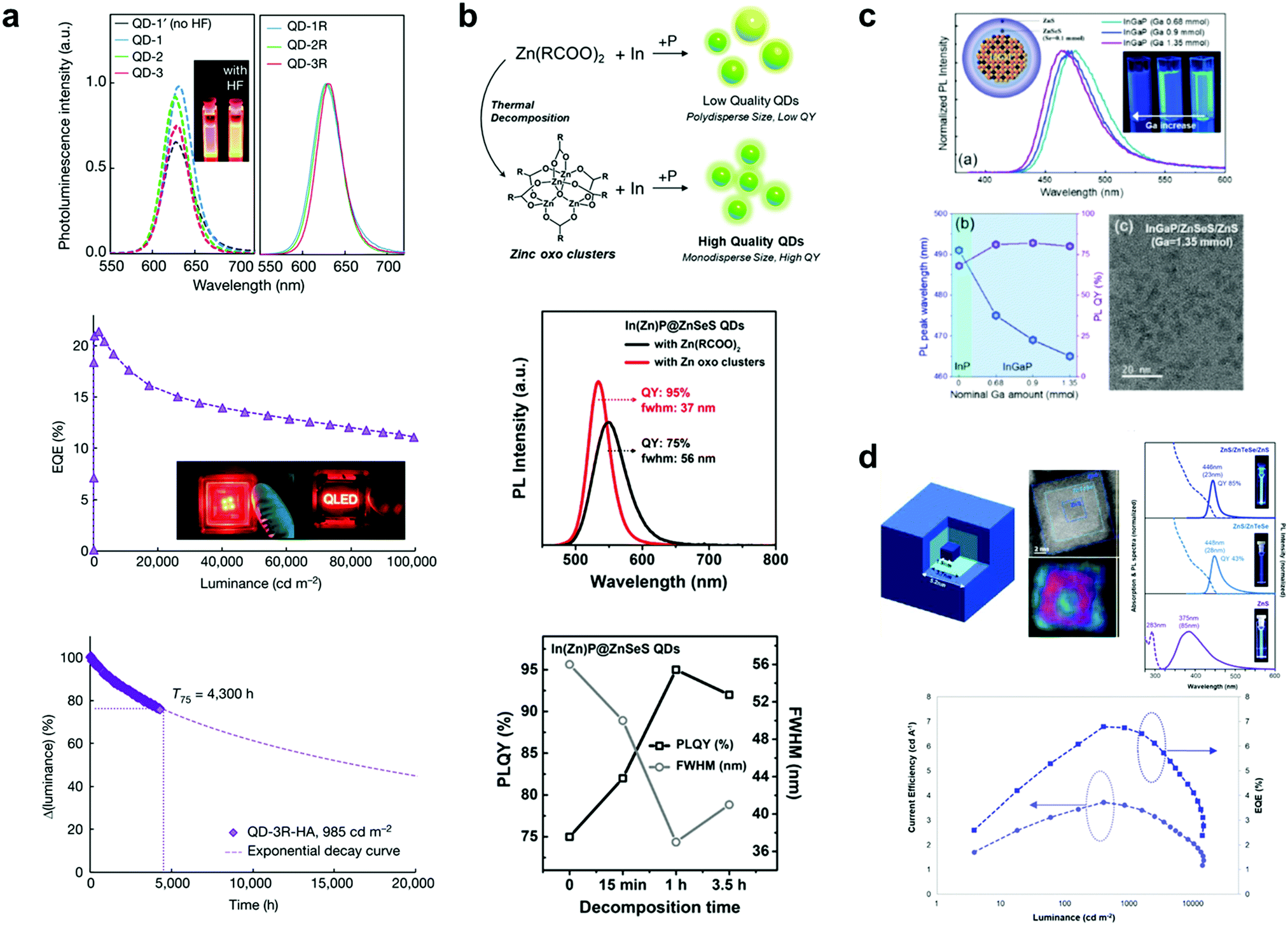 | ||
| Fig. 3 (a) Red colour-emitting InP QDs. PL spectra without and with HF treatment. EQE and lifetime measurement results of the red InP-based QLED. Copyright 2019, Nature Publishing Group. (b) Green colour-emitting InP QDs. Reaction mechanism of the Zn-oxo complex-mediated reaction for the synthesis of InP QDs. PLQY and the FWHM tendency versus ratio of the Zn-oxo complex. (c) Normalised PL spectrum, PLQY and PL peak wavelength of blue InGaP alloy QDs as a function of Ga amount. (d) Schematic illustration of the Zn/ZnTeSe/Zn CQW structure, absorption and PL spectra, EQE and current efficiency as a function of luminance. Copyright 2020, the American Chemical Society. | ||
In addition to the development of InP-based QDs, Kim et al. introduced quantum well-structured ZnS/ZnTeSe/ZnS QDs as blue QDs, as shown in Fig. 3(d).34 Normally, ZnTeSe is used as an emissive core material for blue QDs and ZnS is used as the shell material covering the core materials. However, the distribution of the particle size of the ZnTeSe/ZnS (core/shell) QDs was broadened by the different reactivities of Te and Se with the Zn precursors, causing a wide FWHM in the PL spectra. To achieve a narrow particle size distribution, ZnS/ZnTeSe/ZnS (core/mid-layer/shell) structured QDs were used instead of ZnTeSe/ZnS (core/shell) QDs. The inner ZnS core with a narrow particle size distribution was prepared, followed by growth of the ZnTeSe mid-layer to prevent lattice mismatch between the core and emissive mid-layer of ZnTeSe. Then, the ZnS shell was coated again to reduce the surface defects and increase the overall stability of the QDs. With this structure, the maximum PLQY of 85% was obtained with the FWHM of 23 nm. Furthermore, the blue-lighting colloidal quantum-well-based LED exhibited an EQE of 6.8% at 3.6 V, and the maximum luminance of 14146 cd m−2.
Device architectures of QD-LEDs
To maximise the use of the aforementioned superior properties of QDs, the device architecture of QD-LEDs has been profoundly studied.3,35 In this section, the evolution of the structural advances of the QD-LED device are summarised. Fig. 4(a) shows the typical device structure and components of QD-LEDs. As shown in Fig. 4(a), QD-LEDs are a stratified structure of several semiconductor layers. They consist of an anode electrode, a hole injection layer (HIL), a hole transport layer (HTL), an emissive layer (EML), an electron transport layer (ETL) and a cathode electrode in sequence.36 Especially, the EML consists of QDs as the emissive material of the LEDs. The QDs in the EML are depicted as green spheres in Fig. 4(a)–(c). For the operation of QD-LEDs, the holes and electrons are transported from the external voltage sources and injected into the QD layer through the HIL/HTL and ETL, respectively. Then, light is emitted from the EML by the radiative recombination process of the excitons generated from the carriers injected into the QD core nanocrystal.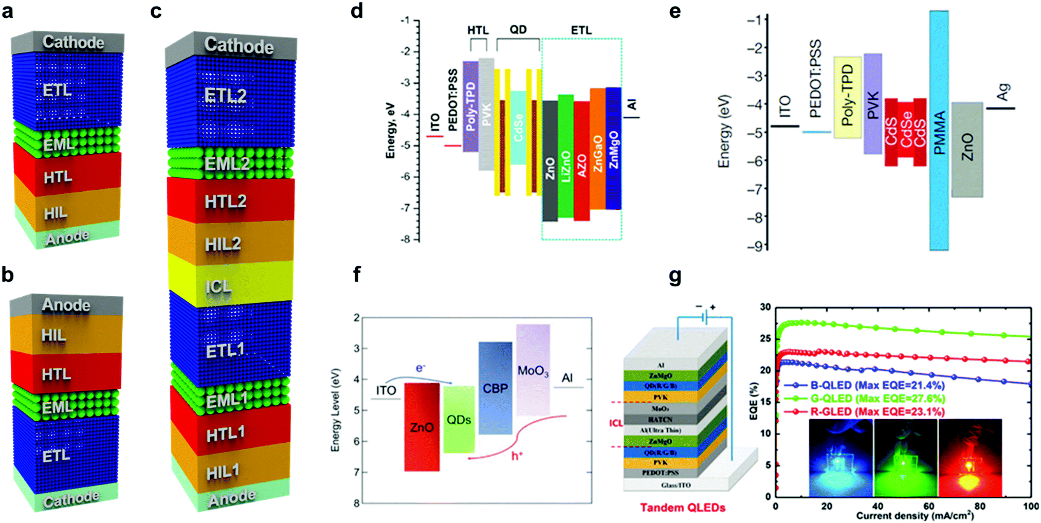 | ||
| Fig. 4 (a) Typical structure and (b) an inverted structure of QD-LED device architecture. (c) Device architecture of tandem structure of QD-LEDs. (d) Energy band diagram of the typical structure of QD-LED devices having different ZnO layers. Copyright 2020, Nature Publishing Group. (e) Energy band diagram of the typical device structure with an insulating layer using PMMA. Copyright 2014, Nature Publishing Group. (f) Energy band diagram of inverted structure of QD-LEDs. Copyright 2019 IOP Publishing. (g) Schematic device structure of tandem QD-LED and the EQE characteristics of red, green, and blue QD-LEDs. Copyright 2014, the American Chemical Society. | ||
Indium tin oxide (ITO) and aluminium (Al) are commonly used as the anode and cathode electrodes, respectively. Poly(3,4-ethylenedioxythiophene)–poly(styrenesulfonate) (PEDOT:PSS) as the HIL, poly[(9,9-dioctylfluorenyl-2,7-diyl)-co-(4,4′-(N-(4-sec-butylphenyl)diphenylamine))] (TFB), poly(4-butyl-phenyldiphenyl-amine) (poly-TPD) and/or poly-N-vinylcarbazole (PVK) as the HTL and zinc oxide (ZnO) NPs as the ETL are widely used as materials in each transport layer.36 There are two types of QD-LED device architectures, namely the typical and inverted structures, as shown in Fig. 4(a) and (b), respectively. The typical structure is widely used for the bottom emission QD-LEDs, which the light through the transparent bottom ITO/glass substrate.27,37,38 However, when an n-type channel oxide thin-film transistor is used as the active-matrix, an inverted QD-LED is preferred owing to its bottom cathode structure.39–42 The architecture of the device can be selected depending on the application and the operation condition of the QD-LEDs. The highly applaudable device tandem structure architecture has been also introduced, as shown in Fig. 4(c), which is used to improve the efficiency of QD-LEDs by vertically stacking several QD-LED units with a transparent interconnecting layer (ICL).30,43–47
Each of the auxiliary layers such as the HIL, HTL and ETL is characterised by the layer thickness, carrier mobility, energy band alignment with their neighbouring layers and interfacial morphologies. It is crucial to develop the layer structure of the device architecture and to optimize the materials and processes of all the layers to achieve high electro-optical performances. Many studies related to the engineering of ETL/HTL components with various materials and fabrication methods have been reported, and recent studies have demonstrated EQE values of QD-LED devices comparable to that of OLEDs.29 However, the enhancement of the device lifetime is still one of the major challenges for the commercialisation of QD-LEDs.
Besides the aforementioned stability of QD materials, the device lifetime is also highly related to the configuration of the layers making up the QD-LED device. In the case of the device, the major factor affecting the performance degradation is the unbalance of charge injection into the QD layer. When the charge injection is unbalanced, QD charging and non-radiative Auger recombination by excessive charges occur in the QD layer, which lead to the degradation of the device.48 The charge injection is determined by various physical parameters such as the carrier mobility, conduction and valence energy levels, carrier concentration and surface morphology of the transport layers. Therefore, by engineering the each of the transport layers to control the charge injection, charge balance can be achieved to maximise the electro-optical performance and longer lifetime. The most relevant reports of device optimisation for higher EQE and longer lifetime of the device are introduced as follows.
Based on the typical device architecture, Shen et al. achieved a high EQE for red, green and blue of 21.6%, 22.9% and 8.05% simultaneously with the high luminance of 13300 cd m−2, 52500 cd m−2 and 10100 cd m−2, respectively.29 They used CdSe/ZnSe (core/shell) QDs for the EML owing to their high quantum yields in solution and better QD layer surface morphology. They also have realized the advance lifetime T50@100 cd m−2 for the red, green and blue QD-LEDs of 1600000 h, 1760000 h and 7000 h, respectively. One of the recent studies on the ETL was reported by Alexandrov et al.49 They investigated the efficient synthetic conditions for ZnO NPs, which are the most popular material for the ETL. The energy diagram of their QD-LED devices is shown in Fig. 4(d). They fabricated QD-LEDs by replacing the ETL with Al-, Ga-, Mg- and Li-doped ZnO NPs. The Al-doped ZnO NPs showed the highest brightness with the lowest turn-on voltage compared to pure ZnO and Ga-, Mg-, Li-doped NPs owing to the high electron conductivity and the low roughness of their surface morphology. Fig. 4(e) shows the device architecture suggested by Dai et al. to enhance the electro-optical performance of QD-LEDs.50 They demonstrated an efficient red QD-LED by inserting a hole blocking layer. By providing the hole blocking layer between the EML and ETL using 6 nm of PMMA, excessive hole carriers from the anode were effectively blocked, resulting in an increase in the device efficiency. The red QD-LED with the CdSe/CdS (core/shell) QDs exhibited a turn-on voltage of 1.7 V, EQE of 20.5%, and a lifetime T50@100 cd m−2 of more than 100000 h.
The inverted structure in Fig. 4(b) was also engineered by Sun et al. to improve the light efficiency by introducing an interfacial modification layer (IML) between ZnO and the QDs.28 The IML has the function of blocking the excessive charges and passivating defects in ZnO. They demonstrated red inverted QD-LEDs with a peak EQE of 13.57%, which was obtained by introducing a 13 nm-thick Zn0.85Mg0.15O layer as the IML for suppressing exciton quenching and improving the charge balance of the device. Lee et al. demonstrated another inverted QD-LED structure, which exhibited a reduced leakage current with enhanced device performance.51 The energy band diagram of their device is depicted in Fig. 4(f). An ethylenediaminetetraacetic acid (EDTA) layer was introduced between the ZnO and the QDs for the passivation of defects. A maximum EQE and luminescence of 5.5% and 187186 cd m−2, respectively, were obtained on the inverted QD-LEDs by optimising the thickness of the EDTA layer to passivate the defect states of ZnO.
To break through the EQE of QD-LEDs, a hybrid device tandem structure architecture was reported for further enhancement of QD-LEDs. Zhang et al. showed efficient red, green, and blue tandem structure QD-LEDs, reporting a high EQE in excess of 21% by serially stacking two or more QD-LED units, as shown in Fig. 4(g).52 Multiple QD-LED devices were interconnected by a transparent ICL. This device exhibited a high current efficiency and EQE of 41.5 cd A−1 and 23.1% for red, 121.5 cd A−1 and 27.6% for green, and 17.9 cd A−1 and 21.4% for blue QD-LEDs, respectively.
Innovative fabrication processes
As elaborated in the previous sections, QD-LEDs are a stratified structure of organic and inorganic materials. Each of their functional layers is tens of nanometres thick. To form the stratified layer structure of QD-LEDs, the most widely used fabrication process is spin-coating.53 The spin-coating process is schematically illustrated in Fig. 5(a). Spin-coating is useful to form uniform thin films with a nanoscale thickness. Especially, the electro-optical performances such as light efficiency and brightness of QD-LEDs is highly affected by the film thickness and quality of the QD layer. QDs have a small size below 10 nm in diameter, and the QD layers should be formed to be as thin as possible in order to achieve high efficiency and brightness.54 The thickness of the QD layer is determined by the concentration of material solution and the rotational speed during the spin-coating process. However, to adapt the solution process to large-sized applications such as displays and lighting systems, a uniform thickness with good surface morphology should be pursued in terms of film quality, which is known to affect the performance of QD-LEDs.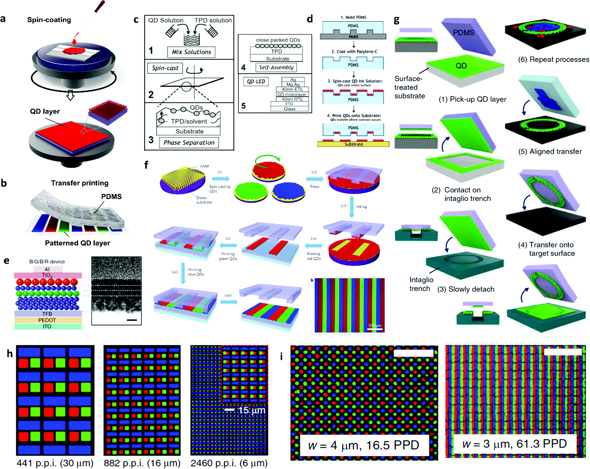 | ||
| Fig. 5 Schematic illustration of the fabrication process for (a) spin-coating, (b) transfer printing of the QD layer, (c) formation of QD monolayer by phase separation, and (d) contact printing process of QD layer. Copyright 2005, Wiley-VCH and Copyright 2007, the American Chemical Society. (e) Cross-section TEM image of EL device with layer-by-layer stacking for WLED. Copyright 2013, Nature Publishing Group. (f) Schematic illustration of transfer printing. Copyright 2011, Nature Publishing Group. (g) High-resolution intaglio transfer printing and (h) PL images of full-colour RGB QD via intaglio transfer printing technique. 2015, Nature Publishing Group. (i) PL images of full-colour RGB QD via immersion transfer printing technique. Copyright 2020, Nature Publishing Group. | ||
Furthermore, for realising full-colour display applications with EL-driving QD-LEDs, the red, green and blue QDs should be formed as separate subpixels to maximise the utility of the superior properties of QDs.54–57Fig. 5(b) shows a schematic illustration of QD layer patterning via the transfer printing technique. The innovative technologies for the patterning pixels of QD-LEDs are introduced in this section. To achieve the ultimate performance in EL-based devices, it is important to deposit a very thin layer of ordered QDs. Coe-Sullivan et al. demonstrated a large-area ordered QD monolayer via phase separation during the spin-coating process, as shown in Fig. 5(c).58 Their unique method allowed the fabrication of a monolayer with the maximum grain size of over a square micrometre within seconds. According to the reported results, it is claimed that macroscale devices can be fabricated by the facile assembly of QD monolayer grains formed by phase separation during the spin-coating process.
Meanwhile, to pattern subpixels of QDs for full-colour display applications, Kim et al. performed a contact printing process to deposit a patterned QD monolayer using microstructured poly-dimethyl siloxane (PDMS), as shown in Fig. 5(d).59 They used a spin-coated PDMS stamp to print QDs onto the target substrate. Their approach realised the clear pattern of monolayer QDs for versatile applications such as full-colour displays and white LEDs by introducing the transfer printing technique to deposit and pattern QD monolayers.
Layer-by-layer transfer printing technology of multiple QD layers was reported by Kim et al., as shown in Fig. 5(e).60 With the reliable transfer printing of the QD monolayers, they proposed a new device architecture for a white QD-LED device by stacking red, green and blue QD layers for the white LED application. They achieved a white QD-LED, yielding CIE coordinates of (0.36, 0.37) with the QD sequence of B/G/B/R for the proposed device. Furthermore, as shown in Fig. 5(f), Kim et al. also demonstrated a 4 inch full-colour QD display via the transfer printing technique and its flexible form using a hafnium indium zinc oxide thin-film transistor backplane with a 320 × 240 pixel array.61 The independent donor substrates with self-assembly monolayer (SAM) treatment enabled the transfer-printing of uniform monolayers of red, green and blue QDs to the target substrate. However, the transfer printing technique requires further research to precisely fabricate higher pixel resolutions.
For the application of wearable near-eye displays, the pixel size should be further minimized. Using the intaglio transfer printing technique, Choi et al. successfully demonstrated red, green and blue pixels with high resolutions of up to 2460 pixels per inch and showcased a feature as small as 5 μm, as shown in Fig. 5(g) and (h).62 Instead of the patterned PDMS, they introduced an intaglio trench to remove the undesirable area on the QD layer of flat PDMS and transferred the defined QD layers onto the target substrate. Nam et al. achieved a submicron-sized pattern for full-colour pixel arrays via immersion transfer printing, as shown in Fig. 5(i).63 These innovative fabrication methods are highlighted in terms of pixel patterning to bring attention to emerging real-life applications in the field of portable/large-scale displays.
Conclusions
In this focus article, the recent progress on QD-LED technologies was investigated in terms of the synthesis of QDs, device optimization and fabrication process innovation. For the synthesis of QD materials, a PLQY of more than 95% and a spectrum FWHM of around 20 nm have been achieved by engineering the shell layer and the surface-binding ligand of QDs. The innovative heavy-metal free QDs also show the high commercialisation potential of QD-LEDs for display applications. For the device architecture of QD-LEDs, there are three types of device structures, which are categorised as typical, inverted and tandem structures. By optimisation and passivation of the ZnO ETL, the maximum performance of more than 20% EQE and lifetime of 100000 h have been achieved. Based on the architectural improvement such as the tandem structure, an EQE of over the 20% for red, green and blue QD-LEDs has been also achieved. Finally, for the fabrication process technologies of QD-LEDs, the advanced solution process and patterning processes show the possibilities of the successful application of QD-LEDs in full-colour displays. With the innovative transfer printing technology, the pixel patterning of red, green and blue QDs on the active-matrix backplane has been successfully implemented. The achievements of selected research activities are summarised in Table 1. By the combination of the recent innovative technologies such as the synthesis of QD materials, device engineering and fabrication processes, the successful industrialisation of QD-LEDs for full-colour displays and smart lighting applications is expected in the near future.
| Ref. | Method | Performance summary | |
|---|---|---|---|
| QD materials | |||
| Pal et al.23 | CdSe | Optimization of shell thickness (giant shell concept) | Luminance 1000 cd m−2, turn-on voltage 3.0 V |
| Chen et al.24 | CdSe | Shell coating kinetics control for suppression of lattice mismatch | FWHM 20 nm, PLQY 97% |
| Pu et al.26 | CdSe | Electrochemically stable ligands | T95@1000 cd m−2 > 3800 h for red T50@100 cd m−2 > 10000 h for blue |
| Won et al.31 | InP-red | HF-based surface etching for effective shell coating | PLQY 98%, EQE 21.4%, T50@100 cd m−2 > 1000000 h |
| Kim et al.32 | InP-green | Zn-oxo cluster for reaction rate control | PLQY 95% |
| Kim et al.33 | InP-blue | Ga alloyed InP core | Wavelength 465 nm, PLQY 80%, luminance 1,038 cd m−2, EQE 2.5% |
| Kim et al.34 | ZnTeSe-blue | ZnS/ZnTeSe/ZnS quantum well structure | FWHM 23 nm, luminance 14146 cd m−2 EQE 6.8% at 3.6 V |
| Device architectures | |||
| Shen et al.29 | Typical structure | CdSe/ZnSe QD with high surface morphology | Luminance 13330 cd m−2, EQE 21.6% for red |
| Luminance 52500 cd m−2, EQE 22.9% for green |
|||
| Luminance 10100 cd m−2, EQE 8.05% for blue |
|||
| T50@100 cd m−2 > 1600000 h for red |
|||
| T50@100 cd m−2 > 1760000 h for green |
|||
| T50@100 cd m−2 > 7000 h for blue | |||
| Alexandrov et al.49 | Typical structure | Al-doped ZnO NP for ETL | — |
| Dai et al.51 | Typical structure | PMMA hole blocking layer | EQE 20.5%, turn-on voltage 1.7 V, T50@100 cd m−2 100000 h |
| Sun et al.28 | Inverted structure | IML between ZnO/QD layers | EQE 13.57% |
| Lee et al.51 | Inverted structure | EDTA between ZnO/QD layers | Luminance 187186 cd m−2, EQE 5.5% |
| Zhang et al.52 | Tandem structure | Stacking multiple QD-LED devices | Current efficiency 41.5 cd A−1, EQE 23.1% for red |
| Current efficiency 121.5 cd A−1, EQE 27.6% for green | |||
| Current efficiency 17.9 cd A−1, EQE 21.4% for blue | |||
| Fabrication processes | |||
| Coe-Sullivan et al.58 | Spin-coating | Phase separation during spin-coating process | Grain size of ordered colloidal QD monolayer >1 μm2 |
| Kim et al.59 | Transfer printing | QD spin-coating on PDMS | EL-based QD pattern with 25 μm critical dimension |
| Kim et al.60 | Transfer printing | Layer-by-layer transfer printing | White QD-LED with QD stack |
| CIE coordinates (0.36, 0.37) for white lighting | |||
| Kim et al.61 | Transfer printing | SAM treatment | 4 inch full-colour QD display, 320 × 240 pixel array |
| Choi et al.62 | Transfer printing | Intaglio trench | 2460 pixels per inch |
| Nam et al.63 | Transfer printing | Immersion transfer printing | 500 nm pattern of QD layer |
Author contributions
S. Y. B. surveyed the fabrication technologies and wrote the manuscript; Y.-H. S. surveyed the material technologies and wrote the manuscript; X.-B. F. and D.-W. S. surveyed the material technologies; S. L., H. W. C. and T. H. L. surveyed the device technologies; J. Y., S. Z., W. H.-C., C. S. and L. G. O. contributed to the preparation of figures and writing; S. D. H. and S.-M. J. surveyed the device technologies and wrote the manuscript; J. M. K. supervised this work. All the authors discussed and commented on the manuscript.Conflicts of interest
There are no conflicts to declare.Acknowledgements
This research was supported by the European Union under H2020 grant agreement No. 685758 ‘1D-NEON’ and by the Engineering and Physical Sciences Research Council (EPSRC) project EP/P027628/1 ‘Smart Flexible Quantum Dot Lighting’.References
- I. Yagi, N. Hirai, Y. Miyamoto, M. Noda, A. Imaoka, N. Yoneya, K. Nomoto, J. Kasahara, A. Yumoto and T. Urabe, J. Soc. Inf. Disp., 2008, 16, 15–20 CrossRef.
- Z. Yang, M. Gao, W. Wu, X. Yang, X. W. Sun, J. Zhang, H.-C. Wang, R.-S. Liu, C.-Y. Han, H. Yang and W. Li, Mater. Today, 2019, 24, 69–93 CrossRef CAS.
- Y. Sun, Y. Jiang, X. W. Sun, S. Zhang and S. Chen, Chem. Rec., 2019, 19, 1729–1752 CrossRef CAS.
- D. V. Talapin and J. Steckel, MRS Bull., 2013, 38, 685–691 CrossRef CAS.
- A. I. Ekimov and A. A. Onushchenko, JETP Lett., 1981, 34, 345–349 Search PubMed.
- M. K. Choi, J. Yang, T. Hyeon and D.-H. Kim, npj Flexible Electron., 2018, 2(10), 1–14 Search PubMed.
- T. M. Smeeton, E. Angioni, E. A. Boardman, M. Izumi, N. Iwata, Y. Nakanishi and T. Ishida, Proc. Soc. Inf. Display Int. Symp., 2019, 742–745 CrossRef CAS.
- V. L. Colvin, M. C. Schlamp and A. P. Allvlsatos, Nature, 1994, 370 Search PubMed.
- Y. Shirasaki, G. J. Supran, M. G. Bawendi and V. Bulović, Nat. Photonics, 2012, 7, 13–23 CrossRef.
- V. Wood and V. Bulovic, Nano Rev., 2010, 1(1), 5202 CrossRef.
- W. Guo, J. J. Li, Y. A. Wang and X. Peng, J. Am. Chem. Soc., 2003, 125, 3901–3909 CrossRef CAS.
- J. Zhou, M. Zhu, R. Meng, H. Qin and X. Peng, J. Am. Chem. Soc., 2017, 139, 16556–16567 CrossRef CAS.
- S. Li, M. L. Steigerwald and L. E. Brus, ACS Nano, 2009, 3, 1267–1273 CrossRef CAS.
- A. M. Munro, I. J.-L. Plante, M. S. Ng and D. S. Ginger, J. Phys. Chem. C, 2007, 111, 6220–6227 CrossRef CAS.
- D. C. J. Neo, C. Cheng, S. D. Stranks, S. M. Fairclough, J. S. Kim, A. I. Kirkland, J. M. Smith, H. J. Snaith, H. E. Assender and A. A. R. Watt, Chem. Mater., 2014, 26, 4004–4013 CrossRef CAS.
- X. Wang, T. E. Dykstra, M. R. Salvador, I. Manners, G. D. Scholes and M. A. Winnik, J. Am. Chem. Soc., 2004, 126, 7784–7785 CrossRef CAS.
- H. Moon, C. Lee, W. Lee, J. Kim and H. Chae, Adv. Mater., 2012, 31, 1804294 CrossRef.
- B. Mahler, N. Lequeux and B. Dubertret, J. Am. Chem. Soc., 2010, 132, 953–959 CrossRef CAS.
- A. M. Munro, J. A. Bardecker, M. S. Liu, Y.-J. Cheng, Y.-H. Niu, I. J.-L. Plante, A. K. Y. Jen and D. S. Ginger, Microchim. Acta, 2007, 160, 345–350 CrossRef.
- R. Wang, Y. Shang, P. Kanjanaboos, W. Zhou, Z. Ning and E. H. Sargent, Energy Environ. Sci., 2016, 9, 1130–1143 RSC.
- Y. Kim, N. W. Song, H. Yu, D. W. Moon, S. J. Lim, W. Kim, H. J. Yoon and S. Koo Shin, Phys. Chem. Chem. Phys., 2009, 11, 3497–3502 RSC.
- B. Chon, S. J. Lim, W. Kim, J. Seo, H. Kang, T. Joo, J. Hwang and S. K. Shin, Phys. Chem. Chem. Phys., 2010, 12, 9312–9319 RSC.
- B. N. Pal, Y. Ghosh, S. Brovelli, R. Laocharoensuk, V. I. Klimov, J. A. Hollingsworth and H. Htoon, Nano Lett., 2012, 12, 331–336 CrossRef CAS.
- O. Chen, J. Zhao, V. P. Chauhan, J. Cui, C. Wong, D. K. Harris, H. Wei, H. S. Han, D. Fukumura, R. K. Jain and M. G. Bawendi, Nat. Mater., 2013, 12, 445–451 CrossRef CAS.
- S. Wang, C. Querner, T. Emmons, M. Drndic and C. H. Crouch, J. Phys. Chem. B, 2006, 110, 23221–23227 CrossRef CAS.
- C. Pu, X. Dai, Y. Shu, M. Zhu, Y. Deng, Y. Jin and X. Peng, Nat. Commun., 2020, 11, 937 CrossRef CAS.
- Y. Yang, Y. Zheng, W. Cao, A. Titov, J. Hyvonen, J. R. Manders, J. Xue, P. H. Holloway and L. Qian, Nat. Photonics, 2015, 9, 259–266 CrossRef CAS.
- Y. Sun, Y. Jiang, H. Peng, J. Wei, S. Zhang and S. Chen, Nanoscale, 2017, 9, 8962–8969 RSC.
- H. Shen, Q. Gao, Y. Zhang, Y. Lin, Q. Lin, Z. Li, L. Chen, Z. Zeng, X. Li, Y. Jia, S. Wang, Z. Du, L. S. Li and Z. Zhang, Nat. Photonics, 2019, 13, 192–197 CrossRef CAS.
- P. Shen, F. Cao, H. Wang, B. Wei, F. Wang, X. W. Sun and X. Yang, ACS Appl. Mater. Interfaces, 2019, 11, 1065–1070 CrossRef CAS.
- Y. H. Won, O. Cho, T. Kim, D. Y. Chung, T. Kim, H. Chung, H. Jang, J. Lee, D. Kim and E. Jang, Nature, 2019, 575, 634–638 CrossRef CAS.
- K. Kim, Y.-H. Suh, D. Kim, Y. Choi, E. Band, B. H. Kim and J. Park, Chem. Mater., 2020, 32, 2795–2802 CrossRef CAS.
- K.-H. Kim, J.-H. Jo, D.-Y. Jo, C.-Y. Han, S.-Y. Yoon, Y. Kim, Y.-H. Kim, Y. H. Ko, S. W. Kim, C. Lee and H. Yang, Chem. Mater., 2020, 32, 3537–3544 CrossRef CAS.
- S. Kim, J.-A. Kim, T. Kim, H. Chung, S. Park, S.-M. Choi, H.-M. Kim, D.-Y. Chung and E. Jang, Chem. Mater., 2020, 32, 5200–5207 CrossRef CAS.
- S. Coe-Sullivan, W.-K. Woo, J. S. Steckel, M. Bawendi and V. Bulović, Org. Electron., 2003, 4, 123–130 CrossRef CAS.
- K.-H. Lee, J.-H. Lee, H.-D. Kang, B. Park, Y. Kwon, H. Ko, C. Lee, J. Lee and H. Yang, ACS Nano, 2014, 8, 4893–4901 CrossRef CAS.
- J. Zhao, J. Zhang, C. Jiang, J. Bohnenberger, T. Basché and A. Mews, J. Appl. Phys., 2004, 96, 3206–3210 CrossRef CAS.
- Q. Sun, Y. A. Wang, L. S. Li, D. Wang, T. Zhu, J. Xu, C. Yang and Y. Li, Nat. Photonics, 2007, 1, 717–722 CrossRef CAS.
- W. Ji, P. Jing, W. Xu, X. Yuan, Y. Wang, J. Zhao and A. K. Y. Jen, Appl. Phys. Lett., 2013, 103(5), 053106 CrossRef.
- W. Ji, P. Jing, J. Zhao, X. Liu, A. Wang and H. Li, Nanoscale, 2013, 5, 3474–3480 RSC.
- J. Lim, M. Park, W. K. Bae, D. Lee, S. Lee, C. Lee and K. Char, ACS Nano, 2013, 7, 9019–9026 CrossRef CAS.
- C. Jiang, H. Liu, B. Liu, Z. Zhong, J. Zou, J. Wang, L. Wang, J. Peng and Y. Cao, Org. Electron., 2016, 31, 82–89 CrossRef CAS.
- H.-M. Kim, J. Lee, E. Hwang, J. Kim and J. Jang, Proc. Soc. Inf. Display Intl. Symp., 2016, 1480–1483 CrossRef CAS.
- H. Zhang, Y. Feng and S. Chen, ACS Appl. Mater. Interfaces, 2016, 8, 26982–26988 CrossRef CAS.
- H. Zhang, X. Sun and S. Chen, Adv. Funct. Mater., 2017, 27, 1700610 CrossRef.
- H. Zhang, S. Wang, X. Sun and S. Chen, J. Soc. Inf. Disp., 2017, 25, 143–150 CrossRef CAS.
- C. Jiang, J. Zou, Y. Liu, C. Song, Z. He, Z. Zhong, J. Wang, H. L. Yip, J. Peng and Y. Cao, ACS Nano, 2018, 12, 6040–6049 CrossRef CAS.
- W. K. Bae, Y. S. Park, J. Lim, D. Lee, L. A. Padilha, H. McDaniel, I. Robel, C. Lee, J. M. Pietryga and V. I. Klimov, Nat. Commun., 2013, 4, 2661 CrossRef.
- A. Alexandrov, M. Zvaigzne, D. Lypenko, I. Nabiev and P. Samokhvalov, Sci. Rep., 2020, 10, 7496 CrossRef CAS.
- X. Dai, Z. Zhang, Y. Jin, Y. Niu, H. Cao, X. Liang, L. Chen, J. Wang and X. Peng, Nature, 2014, 515, 96–99 CrossRef CAS.
- T. Lee, D. Hahm, K. Kim, W. K. Bae, C. Lee and J. Kwak, Small, 2019, 15, e1905162 CrossRef.
- H. Zhang, S. Chen and X. W. Sun, ACS Nano, 2018, 12, 697–704 CrossRef CAS.
- J. Zhao, J. A. Bardecker, A. M. Munro, M. S. Liu, Y. Niu, I.-K. Ding, J. Luo, B. Chen, A. K.-Y. Jen and D. S. Ginger, Nano Lett., 2006, 6, 463–467 CrossRef CAS.
- A. Rizzo, M. Mazzeo, M. Biasiucci, R. Cingolani and G. Gigli, Small, 2008, 4, 2143–2147 CrossRef CAS.
- A. Carlson, A. M. Bowen, Y. Huang, R. G. Nuzzo and J. A. Rogers, Adv. Mater., 2012, 24, 5284–5318 CrossRef CAS.
- S. Lee, D. Yoon, D. Choi and T. H. Kim, Nanotechnology, 2013, 24, 025702 CrossRef.
- B. H. Kim, S. Nam, N. Oh, S. Y. Cho, K. J. Yu, C. H. Lee, J. Zhang, K. Deshpande, P. Trefonas, J. H. Kim, J. Lee, J. H. Shin, Y. Yu, J. B. Lim, S. M. Won, Y. K. Cho, N. H. Kim, K. J. Seo, H. Lee, T. I. Kim, M. Shim and J. A. Rogers, ACS Nano, 2016, 10, 4920–4925 CrossRef CAS.
- S. Coe-Sullivan, J. S. Steckel, W. K. Woo, M. G. Bawendi and V. Bulović, Adv. Funct. Mater., 2005, 15, 1117–1124 CrossRef CAS.
- L. Kim, P. O. Anikeeva, S. A. Coe-Sullivan, J. S. Steckel, M. G. Bawendi and B. Vladimir, Nano Lett., 2008, 8, 4513–4517 CrossRef CAS.
- T. H. Kim, D. Y. Chung, J. Ku, I. Song, S. Sul, D. H. Kim, K. S. Cho, B. L. Choi, J. M. Kim, S. Hwang and K. Kim, Nat. Commun., 2013, 4, 2637 CrossRef.
- T.-H. Kim, K.-S. Cho, E. K. Lee, S. J. Lee, J. Chae, J. W. Kim, D. H. Kim, J.-Y. Kwon, G. Amaratunga, S. Y. Lee, B. L. Choi, Y. Kuk, J. M. Kim and K. Kim, Nat. Photonics, 2011, 5, 176–182 CrossRef CAS.
- M. K. Choi, J. Yang, K. Kang, D. C. Kim, C. Choi, C. Park, S. J. Kim, S. I. Chae, T. H. Kim, J. H. Kim, T. Hyeon and D. H. Kim, Nat. Commun., 2015, 6, 7149 CrossRef CAS.
- T. W. Nam, M. Kim, Y. Wang, G. Y. Kim, W. Choi, H. Lim, K. M. Song, M. J. Choi, D. Y. Jeon, J. C. Grossman and Y. S. Jung, Nat. Commun., 2020, 11, 3040 CrossRef CAS.
Footnote |
| † These authors contributed equally to this work. |
| This journal is © The Royal Society of Chemistry 2021 |