
 Open Access Article
 This Open Access Article is licensed under a
 Creative Commons Attribution 3.0 Unported Licence
Gas flow-assisted vacuum drying: identification of a novel process for attaining high-quality perovskite films†
Florian
Mathies‡
 *a,
Edgar R.
Nandayapa‡
b,
Gopinath
Paramasivam
a,
Mohammad F.
Al Rayes
b,
Vincent R. F.
Schröder
bc,
Carolin
Rehermann
a,
Emil J. W.
List-Kratochvil
bc and
Eva L.
Unger
ad
*a,
Edgar R.
Nandayapa‡
b,
Gopinath
Paramasivam
a,
Mohammad F.
Al Rayes
b,
Vincent R. F.
Schröder
bc,
Carolin
Rehermann
a,
Emil J. W.
List-Kratochvil
bc and
Eva L.
Unger
ad
aYoung Investigator Group Hybrid Materials Formation and Scaling, Helmholtz-Zentrum Berlin für Materialen und Energie GmbH, Kekuléstraße 5, 12489 Berlin, Germany
bHelmholtz-Zentrum, Berlin für Materialien und Energie GmbH, Hahn-Meitner-Platz 1, 14109 Berlin, Germany
cHumboldt-Universität zu Berlin, Institut für Physik, Institut für Chemie, IRIS Adlershof, Zum Großen Windkanal 2, 12489 Berlin, Germany
dChemical Physics and NanoLund, Lund University, PO Box 124, 22100 Lund, Sweden
First published on 23rd July 2021
Abstract
Controlling the nucleation and crystal growth in solution-processed metal halide perovskite (MHP) thin films is the pivotal point in fabricating homogenous and pinhole-free films. Using scalable coating and printing techniques, vacuum and gas flow-assisted drying processes turn out to be the most promising methods to induce nucleation and crystallization. Yet, the exact interplay and nature of these processes are unclear. In our work, we optically monitor these processes in situ. For the first time, we can show that a controlled venting of the vacuum chamber and the use of a subsequent gas flow are key to achieve homogenous nucleation. Utilizing this gas flow-assisted vacuum drying process, we find that regular, optically dense and pinhole-free MHP layers can be fabricated via inkjet printing, which yield solar cells with a power conversion efficiency of 16%, as compared to 4.5% for vacuum drying.
Introduction
The major challenge to scale MHP solar cell technology to market is to find reliable and scalable methods to attain homogenous pinhole-free large-area films from solution. Over the past years, a large variety of solution-based coating and printing techniques, such as slot-die-coating, blade-coating, spray-coating, inkjet-printing have proven their potential for the fabrication of large-area solar cells and other optoelectronic applications.1–3 To induce and control the crystallization of wet perovskite films, different protocols have been established, such as radiative or temperature annealing,4 antisolvent quenching,5 gas quenching,6–9 and vacuum drying.10–13 While antisolvent quenching is mainly used in spin-coating processes, gas quenching and vacuum drying are widely applied as in-line or post-deposition drying steps along with scalable coating and printing techniques. Especially vacuum drying was established for inkjet-printed layers and it is the most common protocol to produce highly efficient solar cells by crystallizing the wet film at a pressure between 10−2 and 102 mbar.12–15 Based on this effort, power conversion efficiencies (PCE) of close to 20% for partially printed devices,15,16 and more than 17% for fully inkjet-printed solar cells, have been achieved up till now.14 Furthermore, vacuum drying has been successfully used for other scalable methods, such as blade-coating,17,18 spray-coating,19 as well as for spin-coated films.10,20 Regardless of these successes, a detailed review of the formation of MHPs with the vacuum drying process has been lacking in the literature. Also, experimental conditions such as drying time, chamber pressure, chamber size and shape, or pump rate are rarely reported. As such, the vacuum drying mechanism can be explained by the LaMer crystallization and nucleation theory: Fast solvent evaporation under vacuum conditions lead to an oversaturated film with a high nucleation density from which the perovskite crystals grow more homogenous compared to a slower drying film with fewer seed nuclei and irregular growth conditions without vacuum assistance.21–25 Moreover, despite the fact that several studies report that an additional gas flow influences the halide formation, little or no consideration is given to the use of venting of the chamber in the context of MHP formation using vacuum drying processes.26,27 An elegant method to elucidate the film formation of MHPs is optical in situ monitoring.28In this study, we present a detailed and clear picture of the gas flow-assisted vacuum drying (GAVD) process using optical in situ monitoring of the crystallization process. For this, Cs0.05(FA0.83MA0.17)0.95Pb(I0.83Br0.17)3 was printed using a ternary solvent system consisting of dimethylformamide, dimethylsulfoxide, and γ-butyrolactone to meet ink functionality and printing requirements.12,13,29 Utilizing a home-built in situ microscope and photoluminescence (PL) setup,30,31 we monitored for the first time the drying process of inkjet-printed MHP layers under vacuum conditions and subsequent venting of the chamber with a controlled N2 gas flow.
This so-called gas flow-assisted vacuum drying (GAVD) process allowed the fabrication of optically dense and pinhole-free MHP thin-film layers, as depicted in Fig. 1 and Fig. S1 (ESI†).
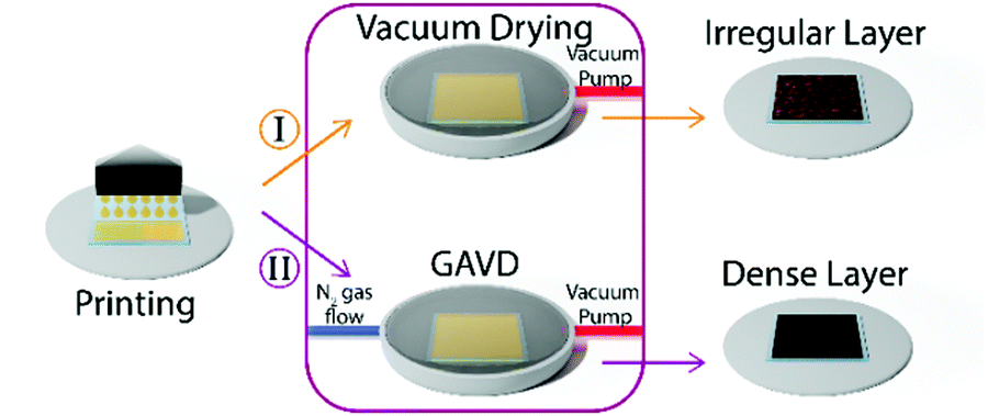 | ||
| Fig. 1 Conventional vacuum drying leads to inhomogeneous perovskite crystallization and irregular thin films (I). By controlling the refilling of the chamber with N2-gas flow, so-called gas flow-assisted vacuum drying (GAVD), optical dense and pinhole-free perovskite layers (II) are achieved. | ||
Results and discussion
Optical in situ study
In Fig. 2, we compare the results of pure vacuum drying to the optimized GAVD process. To monitor the crystallization process, optical images and PL were recorded as a function of process time. Fig. 2(a) and (d) show that vacuum drying at a base pressure of 0.5 mbar required more than 200 s to observe a PL signal and a haziness in the microscopic image due to crystallization. In contrast, a fast crystallization of the wet precursor film was obtained within 35 s for the GAVD process as shown in Fig. 2(b), using an N2 flow at 20 mbar. Tests for optimizing the gas flow conditions are depicted in Fig. S2 (ESI†). The PL in Fig. 2(b) shows that the additional gas flow induced a tremendous change in the evolution of the crystallization onset. The comparison of the PL traces in Fig. 2(c) highlights this again. While the PL peak signal of the GAVD sample increased steeply before going into saturation, the vacuum-dried sample showed a steady linear increase, indicating different crystallization dynamics for each process. Moreover, a strong red-shift of the PL peak position from 690 to 740 nm indicated that the crystal growth process starts from small seed crystals to larger perovskite intermediates during the GAVD process. In contrast, the PL shifted only from 730 to 740 nm for the purely vacuum-dried samples. This narrow red-shift can be explained by the slower supersaturation which does not allow cluster and coordination complexes to completely form, leading only to a partially crystallized material, as discussed by Fateev et al.32 The overall low PL peak of 740 nm at the end of the drying process can be attributed to the competing formation processes of bromide and iodide-rich intermediate phases of the mixed halide MHP composition.31 In both cases, a PL peak of 760 nm is measured after temperature post-annealing. In addition to the PL measurements, we recorded the drying behavior of the samples in situ using an optical microscope. Of particular interest is the crystallization process, where we observed a darker, more hazy, optically denser layer in the GAVD sample as compared to the light brown and cloudy layers from the vacuum-dried sample (see Fig. 2(d and e)). Even more, interestingly, the drying dynamics are different. Vacuum-dried samples dry from the outside to the center of the layer due to the higher surface-to-volume ratio at the sample edges, where the saturation concentration is reached earlier. In contrast, GAVD-treated samples dried much faster and crystallized along the direction of the N2-flow, also indicating that the gas flow as such and not only the increased pressure is highly relevant (video in S1, ESI†).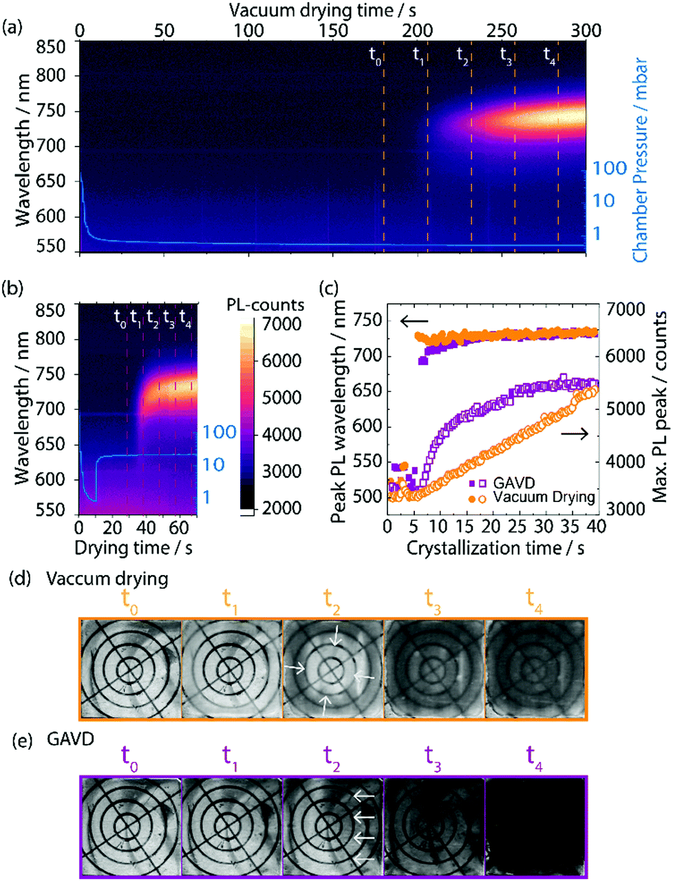 | ||
| Fig. 2 (a) Photoluminescence (PL) signal of vacuum-dried perovskite layer with crystallization onset after around 200 s. (b) PL signal of gas flow-assisted vacuum drying with a crystallization onset after ∼35 s. The chamber pressure is shown in blue as an inset graph. (c) Evolution of the PL peak position and the PL peak height starting from the crystallization onset point. (d) and (e) show microscopic images of the drying behavior at different time stamps. | ||
Morphological impact of the GAVD process
To further investigate the different formation kinetics, we performed X-ray diffraction (XRD) measurements on “wet” and annealed samples, as depicted in Fig. 3(a). After vacuum drying, multiple reflexes from the MA2DMSO2Pb3I8 intermediate phase, indicating a random crystallite orientation, were visible33 as well as reflexes from the tetragonal perovskite phase. In contrast, for the GAVD method, we observed a highly oriented MA2DMSO2Pb3I8 intermediate phase with a dominant peak at 6.7°, corresponding to the 002 orientation, probably resulting from the directed gas flow. In both cases, we see a full conversion to the tetragonal perovskite structure with main reflexes at 14.2° and 28.4° after temperature annealing.34 Also, a notable PbI2-reflexes at 12.7° was visible for both samples, indicating incomplete MHP conversion. Despite the different crystallization and growth conditions, the resulting perovskite structures seem similar. This is due to the strong influence of the later hot-annealing step on the final perovskite crystal transformation and the balance of structural changes. However, morphological changes, such as pinhole density and coverage are largely influenced by the crystallization and nucleation process during the drying step as depicted in Fig. 3(b–e).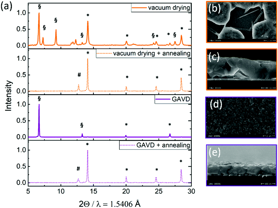 | ||
| Fig. 3 (a) X-ray diffraction patterns of MHP films measured directly after vacuum and GAVD treatment, and collected after temperature annealing at 100 °C. * mark the reflexes of the perovskite tetragonal phases. # marks the PbI2 reflex. § marks the MA2DMSO2Pb3I8 intermediate phase according to Cao et al.33 Scanning electron microscope (SEM) images of vacuum-dried (c and b) and GAVD-treated (d and e) samples after temperature annealing. | ||
Working mechanism of the GAVD process
The presented results clearly show that the deliberate introduction of a controlled gas flow is the crucial process step to produce favorable crystallization in a vacuum drying process for solution-processed MHP films. Including previous findings, this novel so-called gas flow-assisted vacuum drying method can be understood and explained as a multistep process. First, the gas flow enhances the solvent evaporation rate leading to a faster supersaturation process and a more homogeneous formation of crystal seeds what is in line with recent reports.27,35 Secondly, the gas flow accelerates the removal of solvent vapors near the interface, which leads to locally increased concentration at the interface. Hence, the crystallization starts at the solvent/air interface where the gas flow hits the sample first, as mentioned by Chen et al.36 Thirdly, the gas flow induces a higher nucleation rate leading to the formation of a highly oriented metastable crystal phase distributed across the wet film surface,37 from where crystallites grow homogeneously as indicated by the red-shift of the PL peak and the narrow PL peak full width half maximum (Fig. 2c and Fig. S3, ESI†).31 Interestingly, the addition of the gas flow leads to the formation of a highly orientated MA2DMSO2Pb3I8 intermediate phase from where the dense MHP layer grows. Hence, the combination of vacuum drying to drain out excess solvent and anchoring of the printed film and the additional gas flow allows for controlled crystallization and nucleation to form homogenous and pinhole-free perovskite layers.Proof of concept perovskite solar cells
To also demonstrate the viability of the novel GAVD process, inkjet-printed perovskite solar cells in p–i–n architecture have been fabricated and the performance has been compared to devices fabricated using pure vacuum drying. For both cell types, the perovskite layer is inkjet-printed on top of a ([2-(9H-carbazol-9-yl)ethyl]phosphonic acid) self-assembled monolayer (see Fig. S5, ESI† for wetting details).38,39 Using this architecture and GAVD, we right away attain very well-defined pinhole-free perovskite thin films with large grains, achieving a maximum PCE of 16.0% with a high open-circuit voltage of 1.11 V and low hysteresis without further optimization (Fig. 4 and Fig. S6, ESI†). In comparison, purely vacuum-dried samples exhibited low PCEs of up to 4.5% with a low current density and open-circuit voltage, resulting from the irregular morphology and moderate pin-hole dense MHP layers. With this starting point, we are confident that further fine-tuning of the GAVD process parameters, alongside in situ optical monitoring and the further adaptation of carrier extraction layers, will establish GAVD as a reliable and scalable method to fabricate homogenous pin-hole free large-area solar cells from solution with appealing performances.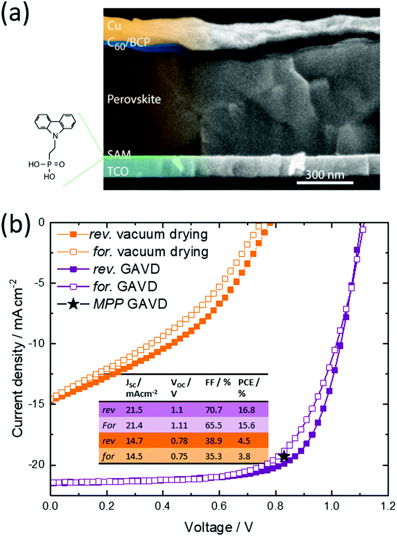 | ||
| Fig. 4 (a) Solar cell architecture on p–i–n architecture. The Perovskite layer is inkjet-printed with the GAVD process. (b) Current density-voltage characteristics and of inkjet-printed perovskite solar cells on SAM using vacuum drying and GAVD method. Value for mpp-tracking (16%) is the average over 300 s of tracking the power output. | ||
Conclusions
In summary, using in situ characterization techniques, we for the first time have elucidated the crystallization dynamics of inkjet-printed perovskite layers under different vacuum drying conditions. Contrary to the previously accepted idea that vacuum drying is the major contributor to the MHP crystallization, we demonstrated that a decisive crystallization process is induced by an additional gas flow over the sample. Astonishingly, different crystallization dynamics occur during each one of the drying conditions. The novel process of gas-assisted vacuum drying is the consequent advancement of the simple venting step to control and accelerate the drying conditions of printed MHP thin films. We see strong evidence that the additional gas flow induces a favorable film formation through increased nucleation density at the wet film surface. Nevertheless, further detailed analysis is necessary to fully understand the drastic changes recorded in the resulting printed layers, and with this, establish the process to achieve performing larger area solar cells.Experimental
Materials
The solvents dimethyl formamide (DMF, 99.8%), dimethyl sulfoxide (DMSO, 99.9%), and γ-Butyrolacetone (99.8%) were purchased from Sigma-Aldrich. Lead bromide (PbBr2, 99.99%) and lead iodide (PbI2, 99.99%) were purchased from TCI Deutschland GmbH. Cesium iodide (CsI) was also purchased from Sigma-Aldrich. Methylammonium bromide (MABr) and formamidinium iodide (FAI) were purchased from Dyenamo. [2-(9H-carbazol-9-yl)ethyl]phosphonic acid (2PACz) was purchased from Tokio Chemical Industry (TCI). Patterned indium tin oxide (ITO) glass substrates (25 × 25 mm, resistivity = 15 Ω sq−1, nominal ITO thickness = 150 nm) were purchased by Automatic Research GmbH. C60 (99.99%) and BCP were purchased from Sigma Aldrich, Cu shots from Alfa Aesar.Perovskite solution
PbI2 (1.5 M) was dissolved in 0.8 ml DMF and 0.2 ml DMSO, PbBr2 (1.5 M) dissolved in 0.16 ml DMF and 0.04 ml DMSO. These two solutions were stirred overnight at 60 °C in an inert atmosphere. FAI powder was mixed into the prepared PbI2 solution (1![[thin space (1/6-em)]](https://www.rsc.org/images/entities/char_2009.gif) :1.09 molar ratio) and MABr powder was mixed into the prepared PbBr2 solution (1:1.09 molar ratio). The solutions were shaken for few minutes until the organo-halide powders were fully dissolved. These solutions were mixed to form (MA,FA)Pb(I,Br)3 precursor solution. CsI (1.5 M) was dissolved in 1 ml DMSO stirred overnight at 60 °C in the inert atmosphere. The “Triple cation” perovskite precursor solution was prepared by adding 5 vol% of the CsI solution to the (MA,FA)Pb(I,Br)3 precursor solution. The resulting precursor solution should hence have a stoichiometry of Cs0.05MA0.16A0.79PbBr0.51I2.49.
:1.09 molar ratio) and MABr powder was mixed into the prepared PbBr2 solution (1:1.09 molar ratio). The solutions were shaken for few minutes until the organo-halide powders were fully dissolved. These solutions were mixed to form (MA,FA)Pb(I,Br)3 precursor solution. CsI (1.5 M) was dissolved in 1 ml DMSO stirred overnight at 60 °C in the inert atmosphere. The “Triple cation” perovskite precursor solution was prepared by adding 5 vol% of the CsI solution to the (MA,FA)Pb(I,Br)3 precursor solution. The resulting precursor solution should hence have a stoichiometry of Cs0.05MA0.16A0.79PbBr0.51I2.49.
Device fabrication
Patterned ITO glass substrates were cleaned sequentially for 15 min with a 2% Mucasol solution in water (Schülke), water, acetone, and Isopropanolat ∼ 40 °C in an ultrasonic bath. After that, directly before HTM deposition, the substrates were treated in an UV-ozone cleaner for 15 min UV treatment. All subsequent procedures were done in a nitrogen-filled glovebox (MBRAUN).SAM powders were dissolved in anhydrous Ethanol at a concentration of 3 mmol l−1 and put into an ultrasonic bath for 15 min (30–40 °C) before using. 2PACz powder (molar weight 335.3 g mol−1) was stored in a nitrogen glovebox, The SAMs were prepared by spin-coating. 100 μl of the solution was uniformly released onto the middle of the substrate, the lid was closed and after ∼5 s resting, the spin-coating program (30 s at 3000 rpm) was started. After spin-coating, the substrates were heated at 100 °C for 10 min. The stock precursor solution was diluted prior to the printing process to 0.42 M with a solvent ratio of 60:15:25 (DMF:DMSO:GBL). The perovskite ink was printed onto the substrate using an LP50 inkjet printer (Meyer Burger) equipped with a Spectra SE128 printhead (Fujifilm) inside a nitrogen-filed glovebox. The ink temperature was held at 30 °C during the printing process. The drops (80pL) were created with a single bias pulse at a width of 8 μs and peak voltage of 80 V. All films were printed at a resolution of 300 dpi. After printing, the substrates were transferred to a vacuum chamber (@20 mbar 0.16 L s−1), followed by thermal annealing at 100 °C for 60 minutes. After perovskite deposition, 23 nm C60 and 8 nm BCP were thermally evaporated in a MBRAUN ProVap3G at a base pressure of 10−6 mbar with an evaporation rate of 0.1–1.0 Å s−1. For completing the device, 100 nm Cu was thermally evaporated through a shadow mask. The overlap of the substrate's ITO with the Cu stripe defines the active area of 0.16 cm2.
Thin film characterization
X-ray diffraction (XRD) measurements were done in air with a Bruker D8 Advanced XRD machine using a copper K-α source in Bragg–Brentano geometry. Scanning electron microscopy (SEM) images were recorded with a Hitachi S-4100 and 5 kV acceleration voltage system. The resulting film thickness was verified by profilometry (Bruker Dektak).Optoelectronic characterization
J–V scans were performed as 4-point measurements with a Keithley 2600 SMU controlled by a measurement control program written in LabView. The voltage values are swept in 20 mV steps with an integration time of 40 ms per point and settling time of 20–40 ms after voltage application.In situ-setup
An Ocean Insight part QR400-7-UV-BX reflectance probe is used to collect the optical signals, and is placed at ∼1 cm from the substrates. Ocean optics Flame FLMS12200 spectrometer is used to detect these signals at an integration time of 300 ms. As excitation source, a 415 nm line of a filtered fiber-coupled tungsten-halogen light source (Thorlabs’ SLS201LM) was used.Conflicts of interest
There are no conflicts to declare.Acknowledgements
This work was carried out in the framework of the Joint Lab GEN_FAB and with the support of the Helmholtz Innovation Lab HySPRINT. The authors gratefully acknowledge Carola Klimm for SEM measurements and Paul Zybarth for experimental help with the vacuum drying chamber. F. M., E. L. U. acknowledge funding from the German Ministry of Education and Research for the Young Investigator Group Hybrid Materials Formation and Scaling (HyPerFORME) within the program “NanoMatFutur” (03XP0091), as well as the Helmholtz Energy Materials Foundry and PEROSEED (ZT-0024) project.References
- F. Mathies, E. J. W. List-Kratochvil and E. L. Unger, Energy Technol., 2019, 1900991 Search PubMed.
- F. Hermerschmidt, F. Mathies, V. R. F. Schröder, C. Rehermann, N. Z. Morales, E. L. Unger and E. J. W. List-Kratochvil, Mater. Horiz., 2020, 7, 1773–1781 RSC.
- H. Mescher, F. Schackmar, H. Eggers, T. Abzieher, M. Zuber, E. Hamann, T. Baumbach, B. S. Richards, G. Hernandez-Sosa, U. W. Paetzold and U. Lemmer, ACS Appl. Mater. Interfaces, 2020, 12(13), 15774–15784 CrossRef CAS PubMed.
- S. Sanchez, X. Hua, N. Phung, U. Steiner and A. Abate, Adv. Energy Mater., 2018, 8, 1–7 CAS.
- N. J. Jeon, J. H. Noh, Y. C. Kim, W. S. Yang, S. Ryu and S. Il Seok, Nat. Mater., 2014, 13, 897–903 CrossRef CAS PubMed.
- Y. Deng, C. H. Van Brackle, X. Dai, J. Zhao, B. Chen and J. Huang, Sci. Adv., 2019, 5, 1–9 Search PubMed.
- D.-K. Lee, D.-N. Jeong, T. K. Ahn and N.-G. Park, ACS Energy Lett., 2019, 2393–2401 CrossRef CAS.
- G. Cotella, B. Jenny, D. Francesca, P.-P. Cameron, C. Matthew and W. Trystan, Sol. Energy Mater. Sol. Cells, 2016, 159, 362–369 CrossRef.
- J. Li, J. Dagar, O. Shargaieva, M. Flatken, H. Köbler, M. Fenske, C. Schultz, B. Stegemann, J. Just, D. Többens, A. Abate, R. Munir and E. Unger, Adv. Energy Mater., 2021, 11, 2003460 CrossRef CAS.
- X. Li, D. Bi, C. Yi, J.-D. Décoppet, J. Luo, S. M. Zakeeruddin, A. Hagfeldt and M. Grätzel, Science, 2016, 353, 58 CrossRef CAS PubMed.
- L. Zeng, S. Chen, K. Forberich, C. J. Brabec, Y. Mai and F. Guo, Energy Environ. Sci., 2020, 13, 4666–4690 RSC.
- F. Mathies, T. Abzieher, A. Hochstuhl, K. Glaser, A. Colsmann, U. W. Paetzold, G. Hernandez-Sosa, U. Lemmer and A. Quintilla, J. Mater. Chem. A, 2016, 4, 19207–19213 RSC.
- F. Mathies, H. Eggers, B. S. Richards, G. Hernandez-Sosa, U. Lemmer and U. W. Paetzold, ACS Appl. Energy Mater., 2018, 1, 1834–1839 CrossRef CAS.
- F. Schackmar, H. Eggers, M. Frericks, B. S. Richards, U. Lemmer, G. Hernandez-Sosa and U. W. Paetzold, Adv. Mater. Technol., 2021, 6, 2000271 CrossRef CAS.
- H. Eggers, F. Schackmar, T. Abzieher, Q. Sun, U. Lemmer, Y. Vaynzof, B. S. Richards, G. Hernandez-Sosa and U. W. Paetzold, Adv. Energy Mater., 2020, 10, 1903184 CrossRef CAS.
- Z. Li, P. Li, G. Chen, Y. Cheng, X. Pi, X. Yu, D. Yang, L. Han, Y. Zhang and Y. Song, ACS Appl. Mater. Interfaces, 2020, 12, 39082–39091 CrossRef CAS PubMed.
- F. Guo, S. Qiu, J. Hu, H. Wang, B. Cai, J. Li, X. Yuan, X. Liu, K. Forberich, C. J. Brabec and Y. Mai, Adv. Sci., 2019, 6, 1901067 CrossRef PubMed.
- S. J. Yin, J. Li and N. Zheng, J. Mater. Chem. A, 2019, 7, 26849 RSC.
- J. E. Bishop, J. A. Smith, C. Greenland, V. Kumar, N. Vaenas, O. S. Game, T. J. Routledge, M. Wong-Stringer, C. Rodenburg and D. G. Lidzey, ACS Appl. Mater. Interfaces, 2018, 10, 39428–39434 CrossRef CAS PubMed.
- F. Zabihi, Y. Xie, S. Gao and M. Eslamian, Appl. Surf. Sci., 2015, 338, 163–177 CrossRef CAS.
- W. A. Dunlap-Shohl, Y. Zhou, N. P. Padture and D. B. Mitzi, Chem. Rev., 2018, 119, 3193–3295 CrossRef PubMed.
- V. K. Lamer and R. H. Dinegar, J. Am. Chem. Soc., 1950, 72, 4847–4854 CrossRef CAS.
- M. Jung, S.-G. Ji, G. Kim and S. Il Seok, Chem. Soc. Rev., 2019, 48, 2011–2038 RSC.
- Y. Zhou, O. S. Game, S. Pang and N. P. Padture, J. Phys. Chem. Lett., 2015, 6, 4827–4839 CrossRef CAS PubMed.
- H. Ko, D. H. Sin, M. Kim and K. Cho, Chem. Mater., 2017, 29, 1165–1174 CrossRef CAS.
- B. Ding, Y. Li, S.-Y. Huang, Q.-Q. Chu, C.-X. Li, C.-J. Li and G.-J. Yang, J. Mater. Chem. A, 2017, 5, 6840–6848 RSC.
- L.-L. Gao, C.-X. Li, C.-J. Li and Y. Guan-Jun, J. Mater. Chem. A, 2017, 5, 1548–1557 RSC.
- K. Schötz and F. Panzer, J. Phys. Chem. A, 2021, 125, 2209–2225 CrossRef.
- Y. Seo, E. Kim, S. Cho, S. Kim and S. Na, Appl. Mater. Today, 2017, 9, 598–604 CrossRef.
- A. Merdasa, C. Rehermann, K. Hirselandt, J. Li, O. Maus, F. Mathies and T. Unold, Res. Sq. DOI:10.21203/rs.3.rs-102041/v1.
- C. Rehermann, A. Merdasa, K. Suchan, V. Schröder, F. Mathies and E. L. Unger, ACS Appl. Mater. Interfaces, 2020, 12, 30343–30352 CrossRef CAS PubMed.
- S. A. Fateev, A. A. Petrov, V. N. Khrustalev, P. V. Dorovatovskii, Y. V. Zubavichus, E. A. Goodilin and A. B. Tarasov, Chem. Mater., 2018, 30, 5237–5244 CrossRef CAS.
- J. Cao, X. Jing, J. Yan, C. Hu, R. Chen, J. Yin, J. Li and N. Zheng, J. Am. Chem. Soc., 2016, 138, 9919–9926 CrossRef CAS PubMed.
- M. Saliba, T. Matsui, J.-Y. Seo, K. Domanski, J.-P. Correa-Baena, M. K. Nazeeruddin, S. M. Zakeeruddin, W. Tress, A. Abate, A. Hagfeldt and M. Grätzel, Energy Environ. Sci., 2016, 9, 1989–1997 RSC.
- Y. Zhou, O. S. Game, S. Pang and N. P. Padture, J. Phys. Chem. Lett., 2015, 6(23), 4827–4839 CrossRef CAS.
- S. Chen, X. Xiao, B. Chen, L. L. Kelly, J. Zhao, Y. Lin, M. F. Toney and J. Huang, Sci. Adv., 2021, 26–29 Search PubMed.
- H. Fang, M. F. Hagan and W. B. Rogers, Proc. Natl. Acad. Sci. U. S. A., 2020, 117, 27927–27933 CrossRef CAS PubMed.
- A. Al-Ashouri, A. Magomedov, M. Roß, M. Jošt, M. Talaikis, G. Chistiakova, T. Bertram, J. A. Márquez, E. Köhnen, E. Kasparavičius, S. Levcenco, L. Gil-Escrig, C. J. Hages, R. Schlatmann, B. Rech, T. Malinauskas, T. Unold, C. A. Kaufmann, L. Korte, G. Niaura, V. Getautis and S. Albrecht, Energy Environ. Sci., 2019, 12, 3356–3369 RSC.
- A. Al-Ashouri, E. Köhnen, L. Bor, A. Magomedov, H. Hannes, P. Caprioglio, J. A. Márquez, A. B. Morales Vilches, E. Kasparavicius, J. A. Smith, N. Phung, M. Dorothee, M. Grischek, L. Kegelmann, D. Skroblin, C. Gollwitzer, T. Malinauskas, M. Jost, M. Gasper, B. Rech, R. Schlatmann, M. Topic, L. Korte, A. Abate, B. Stannowski, D. Neher, M. Stolterfoht, T. Unold, V. Getautis and S. Albrecht, Science, 2020, 370, 1300–1309 CrossRef CAS PubMed.
Footnotes |
| † Electronic supplementary information (ESI) available. See DOI: 10.1039/d1ma00494h |
| ‡ These authors contributed equally to this work. |
| This journal is © The Royal Society of Chemistry 2021 |