DOI:
10.1039/D1MA00377A
(Review Article)
Mater. Adv., 2021,
2, 5274-5299
Organolead halide perovskites beyond solar cells: self-powered devices and the associated progress and challenges
Received
24th April 2021
, Accepted 28th June 2021
First published on 30th June 2021
Abstract
Conventional electronic devices powered by lithium-ion batteries or supercapacitors face the challenge of offering long-term and self-sustaining operations. Self-powered devices based on emerging energy harvesting technologies can help of the development of long-lasting transducers with a small form factor. Organolead halide perovskites due to their excellent electro-optical properties are promising photosensitive materials for the development of such self-powered devices. The following review aims at summarizing recent developments made in the field of organolead halide perovskite based self-powered applications. The underlying mechanism driving the self-powered operation in electronic devices such as photodetectors, tactile sensors, and gas sensors is discussed in detail. Finally, the current challenges and prospects of these perovskite based optoelectronic applications are highlighted.

Avi Mathur
| Avi Mathur was born in Khairthal, India. He received his BTech degree in information and communication technology and MTech degree in nanotechnology from the University of Rajasthan, Jaipur. He is currently pursuing a PhD degree in chemistry (nanotechnology) from the University of Waterloo, Canada. Before joining the doctoral program, Avi served as a Project Research Assistant at the Nanoscale Devices Laboratory, Indian Institute of Science, Bangalore, India. He has authored 6 original research articles so far. His research interests include organic–inorganic hybrid perovskites for photovoltaic and optoelectronic device applications. |

Hua Fan
| Hua Fan received her MS in applied chemistry from Beihang University in 2016. She is currently a PhD candidate in chemistry at the University of Waterloo. Her research interests include 1D nanomaterials, flexible devices, and wearable electronics. |

Vivek Maheshwari
| Vivek Maheshwari is an associate professor of chemistry at the University of Waterloo. He is also a member of the Waterloo Institute for Nanotechnology. His group's research is on lead halide perovskite materials for devices and sensors, 1D materials for wearable devices, and nanomaterials for electrocatalysis. He completed his bachelor's degree from the Indian Institute of Technology, Delhi, and his doctorate from Virginia Tech. |
Introduction
With the ongoing continuous advancement in the fields of the Internet of Things (IoT),1–3 portable and wearable electronic devices,4,5 structural monitoring,6,7 and implantable medical devices,8,9 the indispensable dependence of electronic devices and sensors on an external source of power poses a significant challenge. As it stands, electronic devices and sensors, especially those located in remote places, are powered solely by batteries. The limited lifetime of batteries mandates frequent replacement, and, more importantly, batteries also pose a risk of leaking toxic hazardous substances into the environment.10,11 Therefore, concurrently with the current efforts for the miniaturization of sensors and integrated circuits,12 there is an equally critical need for transducers that are capable of operating by harvesting power solely from the ambient environment. Such an approach not only will help in reducing the load drawn from batteries or supercapacitors but can very well eliminate the need for an external power supply as well.
Self-powered devices, as the name indicates, do not need an external power source for their operation. They instead harvest energy needed for their operation from the ambient environment using stimuli such as light, heat, mechanical modulations (e.g. vibrations, stress), and humidity variations.13 With the advancement in the field of designing integrated circuits with low power requirements, an increasing number of electronic devices for a variety of applications are becoming feasible candidates to be self-powered.14–17 Owing to its ability to power devices and sensors even in outdoor and remote locations and its widespread availability, light/solar energy harvesting provides a viable method for energy harvesting.18 Furthermore, presided by the United Nations sustainability development goals, as we look forward towards achieving modern, reliable, and cost-effective energy for all, solar energy harvesting is being considered as one of the most promising technologies for long-term renewable energy production.19 In this pursuit, lead halide perovskites are acknowledged as viable materials for the development of cost-effective and highly efficient photovoltaic systems. The last decade has witnessed an intense research in perovskites solar cells (predominantly with lead-halide based materials), as their certified power conversion efficiency (PCE) has exceeded 25%, up-scaled from just 3.8% within a decade, rivaling that of silicon-based solar cells.20,21 In general, perovskites refer to the class of compounds with a general formula of ABX3 where A and B represent cations of dissimilar sizes while X indicates anion halides, sulfides, and oxides.22 Owing to their photosensitive nature, the focus of attention has been predominantly on the organic–inorganic halide perovskites where A+ represents either a methylammonium (MA+) or formamidinium cation (FA+). The small size of the methylammonium cation (CH3NH3+) leads to the formation of a stable tetragonal phase at room temperature.23 The 3-D framework of MABX3 is devoid of distortion in the MA–X interaction, as otherwise observed in systems involving ethyl ammonium (CH3CH2NH3+) and formamidinium cation (HC(NH2)2+).24 In the context of occupying the B site in the ABX3 system, lead (Pb) has been reported as the superior constituent in comparison to its IV A metal counterparts such as tin (Sn), both in terms of stability and performance and consequentially has been the most widely used metal ion. Ideally, utilization of those with lower atomic numbers (such as Ge or Sn) can be used to lower the energy bandgap of the corresponding perovskite and in addressing the toxicity of Pb, but their utilization is limited by the low intrinsic ionic stability of their divalent oxidation state.25 The halide anion X provides much more freedom of variation in its composition. Iodide (I), lying closest to Pb in the periodic table, shares a similar covalent character and leads to a stable perovskite structure. Upon progressing down the VII A group elements (Cl → I), with an increase in the atomic size of the anion, the absorption spectra shift towards a longer wavelength (redshift) which is attributed to a decrease in electronegativity.24 Hence, chloride and bromide incorporation along with the iodide anion at the X site offers a facile way to tune the bandgap of the halide perovskites. Owing to the exhibition of remarkable properties such as broad absorption spectrum, high absorption coefficient, long carrier lifetime, low trap density, and large diffusion length, organolead halide perovskites (OLHPs) are ideally suited as a material of choice for photovoltaic devices and light energy harvesting.26 For instance, the MAPbI3 tetragonal phase exhibits a suitable bandgap in the range of 1.51–1.55 eV, with an 820 nm absorption edge, exceeding the optimal 1.1–1.4 eV bandgap range governed by the Shockley–Queisser limit for a single-junction solar cell.27 Hence, MAPbI3 is the most typically employed OLHP in photovoltaic applications.
While significant research efforts have been devoted to enhancing the PCE of perovskite solar cells (PSC), new applications of these materials are being researched with increasing efforts, for instance, lasers, light-emitting diodes (LEDs), photodetectors (PDs), gas sensors and tactile sensors.28–33 In the past few years, OLHP based optoelectronic devices and sensors, capable of operating without an external power supply and exhibiting excellent performance, have been actively researched and reported, continuously advancing the field of self-powered devices.34 Therefore, a review focusing on OLHP based self-powered devices will be useful for researchers in this field and also the broader research community. This review provides a detailed discussion of the mechanisms driving self-powered operation in OHLP based electronic devices of varying architecture and their associated figures of merit. Understanding these ongoing developments of perovskite-based self-driven devices will pave the way for further optimization and advancements in this area for future commercialization. A wide array of applications beyond solar cells are discussed where OLHP harvests energy and simultaneously serves as an active layer in an integrated device. A limited discussion focuses on cases where OHLP harvests energy and drives an independent device. Primarily, the latest advancements in PDs, IoTs, transistors, photovoltachromic cells, and sensors are reviewed. Finally, the current challenges of the perovskite-based self-powered devices are presented along with a discussion on future research prospects.
1. Photodetector (PD)
A PD converts an optical input such as visible light photons into an electrical signal35 and has wide-ranging applications in the detection of light intensity, spectral range detection,36 thermal imaging,37 remote imaging,38 and so forth. The significant figures of merit for PDs include responsivity, detectivity, light switching ratio (on/off ratio), spectral selectivity, linear dynamic range, and response time.39 Currently, most of the commercial photodetectors are based on crystalline GaN, Si, and InGaAs.40 The underlying mechanism driving the PD operation is either a p–n (p–i–n) junction, Schottky based, or a photoconductive effect, where the conductivity of the active material increases on interaction with the incident photons. Broad spectral range (190–1100 nm) commercial photodetectors based on the Si p–n junction (photodiodes) (e.g., Hamamatsu S1336) exhibit peak responsivities of 0.12 and 0.5 A W−1 at 200 and 960 nm, respectively, and those designed especially for the visible range (340–720 nm) photometry (e.g., Hamamatsu S8265) exhibit a responsivity of 0.3 A W−1 at the peak sensitivity wavelength of 540 nm, with a dark current of ∼20 pA. These commercial PDs usually require an external power supply and hence need an integrated assembly in the device which can make the device bulky and serve as a bottleneck for utilization in a remote location. Furthermore, these commercial photodiodes need stringent manufacturing controls which limit them to low-volume, high-value markets. To overcome the existing trade-offs between performance, form factor, cost, and most importantly, power consumption, self-powered PDs are being investigated with intense interest.41–43 Self-driven PDs can be obtained when photodiodes work at zero bias, similar to solar cells working under short-circuit conditions. Owing to their excellent electro-optical characteristics, the OLHP based self-powered PDs can offer the benefit of being lightweight with a small device size, without compromising on device performance.44 The early reports on perovskite-based PDs with self-powered characteristics (but did not focus on it exclusively) appeared in 2014 when Dou et al. demonstrated a solution processed ‘inverted’ device (solar cell) configuration PD based on organic–inorganic hybrid CH3NH3PbI3−xClx. The device had a high detectivity of up to 1014 Jones and was capable of operating at 0 V.45 Based on the charge separation mechanism, OLHP PDs can generally be classified into the following categories: p–n (or p–i–n) junction, Schottky junction, polarization effects based, and photoelectrochemical-type PDs. Besides these, an integrated system of energy harvesting units (such as TENG) that drives the light sensitive OLHP to achieve detection can be considered as a distinct type of self-driven PD. The following section summarizes recent advances in PDs driven by these operating mechanisms. Some common strategies that are being employed for enhancing the figures of merit for perovskite PDs have also been discussed. The last subsection is dedicated to flexible OLHP PDs that are now receiving substantial attention as promising candidates for next-generation portable and wearable electronics.
1.1 p–n (or p–i–n) junction-based PDs
The p–n junction-based PDs are the most common type reported so far in the literature. A typical PD with a vertical architecture consists of a perovskite layer sandwiched between an electron transport layer (ETL) and a hole transport layer (HTL) (p–i–n type). It is widely accepted that the interfacial contact properties between the perovskite and transport layers affect the efficiency of photovoltaic devices. Hence, by careful selection of the transport layers, PDs with effective dissociation and transport of photogenerated charge carriers to their respective counter electrode contacts can be fabricated.46 ETLs not only influence the electron transfer and collection but also behave as the hole blocking layer to suppress the electron–hole recombination at the interface.47,48 Significant attention has been paid to ZnO as an electron transport material (ETL) in the early research works reporting OLHP based self-powered PDs. Specifically, morphological tuning of ZnO material was used for the performance optimization of OLHP PDs. Initially, Wang et al. coupled the pyroelectric effect generated in wurtzite ZnO nanowires (NWs) with the photoexcitation ability of MAPbI3.49 The assembly with well-aligned energy band levels led to enhanced charge-carrier separation at the ZnO/perovskite interface. The perovskite also contributed to low dark currents and low background temperature. In the self-powered mode, this UV sensitive heterostructure assembly exhibited 322% enhancement in specific detectivity and responsivity, complemented with five orders of magnitude improvement in the rise time (5.4 s to 53 μs) and fall time (8.9 s to 63 μs) in comparison to devices operating at an applied bias of 0.3 V. The decline in device performance due to applied bias was attributed to the reduced pyro-potential of ZnO NWs owing to the high dark currents and high background temperature. Another report on well-aligned energy levels in the ZnO nanorod (NR)/MAPbI3 heterostructure appeared a year later. Here, Yu et al. used an inorganic metal oxide layer of MoO3 as a hole transport layer to enhance exciton transport while simultaneously protecting the organic perovskite layer.50 The corresponding broadband PD with an appropriate thickness of MoO3 (12 nm) yielded a high detectivity value of 3.56 × 10¹⁴ Jones and 24.3 A W−1 photo-responsivity under 500 nm excitation and no applied bias. Other than preferable band alignment, Zhu et al. proposed the hypothesis that a uniformly distributed blend of ZnO microspheres and nanosheets can effectively utilize the high surface area of microspheres while decreasing series resistance in a vertically configured glass/fluorine doped tin oxide (FTO)/ZnO/MAPbI3/MoO3/Au device.51 Under illumination, the self-driven PD exhibited spectral response from 300 to 800 nm with responsivity and detectivity values reported as high as 48 mA W−1 and 4.5 × 10¹¹ Jones, respectively. The on/off ratio was up to 1400, while the rise time and fall time of the photoresponse were recorded to be 14 and 12 ms, respectively. Despite the facile synthesis process and high electron mobility with increased area of contact of the ZnO NR layer, the photoelectric performance of PDs is generally limited. This is due to the presence of defect states, especially oxygen vacancy which may lead to enhanced charge recombination at the interface between perovskite and ZnO NRs. To primarily reduce the defect density, Zhou et al. doped ZnO with a slightly smaller Ga3+.52 The Ga doped ZnO NR layer (as ETL) served as an effective scaffold with enhanced electron mobility. The resultant HTL-free PD device prepared using graphite electrode had an on/off ratio, a responsivity, and a detectivity of ∼2.5 × 10³, 0.3 A W−1, and 1.3 × 10¹² Jones, respectively. The work by Yang et al. involved the coupling of a MgO/ZnO bilayer with the perovskite layer.53 The ZnO microsphere array scaffold facilitated the penetration of the perovskite into the array and resulted in improved light-harvesting, while MgO passivated the interface between ZnO and perovskite, enhancing stability and carrier transport. Recently, Liu et al. proposed a Cu ion-induced p-type doping in perovskite films by the addition of CuSCN.54 The CH3NH3+ cations from the perovskite film reacted with the SCN− anions from the CuSCN dopant to form HSCN and CH3NH2 by-products, leaving Cu ions to get incorporated into the final perovskite film. The p-type doping facilitated hole transport at the p–n heterojunction interface of perovskite/[6,6]-phenylC61-butyric acid methyl ester (PCBM, ETL) in a self-powered HTL free PD. The authors utilized the optimized PD as a light signal receiver for transmitting text and audio signals in a homemade visible light communication system. Zhou et al. coupled C60 as an ETL along with the perovskite/GaN heterostructure.55 A direct bandgap of 3.4 eV with impressive electro-optical properties, a high carrier mobility, a high melting point, and the chemically stable nature (weak oxidation of N) motivated the authors to choose p-type GaN as the HTL in the hybrid perovskite PD. The high electron mobility and conductivity of C60 enhanced the collection of the electrons along with reduced non-radiative recombination enabling self-powered characteristics. The best performing PD exhibited a responsivity of 0.198 A W−1 and a detectivity of 7.96 × 10¹² Jones with an on/off ratio >5000. To achieve excellent PD device performance, selection of HTL is equally crucial, not only to extract the holes and decrease the dark current density but also to enhance and promote perfect light absorption by the perovskite layer in the whole visible region. Ghosh et al. fabricated an ETL-free self-biased PD inverted device by functionalizing HTL with plasmonic Ag nanoparticles (NPs).56 The plasmon-enhanced optical absorption combined with improvement in charge extraction and transport by Ag NPs was attributed for the enhanced self-powered responsivity in the resultant PD (0.25 A W−1) with a detectivity as high as 1.53 × 10¹¹ Jones. Shin et al. integrated graphene quantum dots (QDs) in both the HTL and photoactive MAPbI3 layer.57 The improved crystallinity of perovskite grains upon the integration of graphene QDs was accredited to the presence of hydrophilic groups including –OH, –COOH, and C![[double bond, length as m-dash]](https://www.rsc.org/images/entities/char_e001.gif) O that leads to the formation of strong bonds within the perovskite film. It was proposed that the addition of graphene QDs increased the work function of the HTL leading to reduced charge recombination at the perovskite/HTL interface. The corresponding self-powered rigid and flexible PDs exhibited detectivities of 8.7 × 10¹² and 8.42 × 10¹² Jones, respectively, with an identical response time of 0.96 μs at 0 V. The flexible PDs displayed appreciable bending stability by maintaining ∼80% of their original responsivity values after repeated bending for 1000 cycles at a radius of 4 mm. Cheng et al. carried out hydrothermal etching of monocrystalline silicon to prepare an array of silicon nanoporous pillars (Si-NPA) which was later used as a substrate as well as a HTL in an inverted assembly of Si-NPA/MAPbI3/ZnO PD.58 The air-stable inorganic HTL enabled the PD to retain 92% performance despite storing the device in ambient air for a month. The template of quasi-identical micron-sized Si pillars offered a large interfacial contact area for incident light while simultaneously reducing the reflection. The authors proposed that the Si-NPA template also effectively enhanced carrier transport and reduced the collection path of the photogenerated carriers leading the self-driven PDs to exhibit a high on/off ratio of 8.2 × 10⁴, a photoresponsivity of 8.13 mA W−1, a specific detectivity of 9.74 × 10¹² Jones, and fast response speeds of 253.3/230.4 μs at zero bias under 780 nm light illumination.
O that leads to the formation of strong bonds within the perovskite film. It was proposed that the addition of graphene QDs increased the work function of the HTL leading to reduced charge recombination at the perovskite/HTL interface. The corresponding self-powered rigid and flexible PDs exhibited detectivities of 8.7 × 10¹² and 8.42 × 10¹² Jones, respectively, with an identical response time of 0.96 μs at 0 V. The flexible PDs displayed appreciable bending stability by maintaining ∼80% of their original responsivity values after repeated bending for 1000 cycles at a radius of 4 mm. Cheng et al. carried out hydrothermal etching of monocrystalline silicon to prepare an array of silicon nanoporous pillars (Si-NPA) which was later used as a substrate as well as a HTL in an inverted assembly of Si-NPA/MAPbI3/ZnO PD.58 The air-stable inorganic HTL enabled the PD to retain 92% performance despite storing the device in ambient air for a month. The template of quasi-identical micron-sized Si pillars offered a large interfacial contact area for incident light while simultaneously reducing the reflection. The authors proposed that the Si-NPA template also effectively enhanced carrier transport and reduced the collection path of the photogenerated carriers leading the self-driven PDs to exhibit a high on/off ratio of 8.2 × 10⁴, a photoresponsivity of 8.13 mA W−1, a specific detectivity of 9.74 × 10¹² Jones, and fast response speeds of 253.3/230.4 μs at zero bias under 780 nm light illumination.
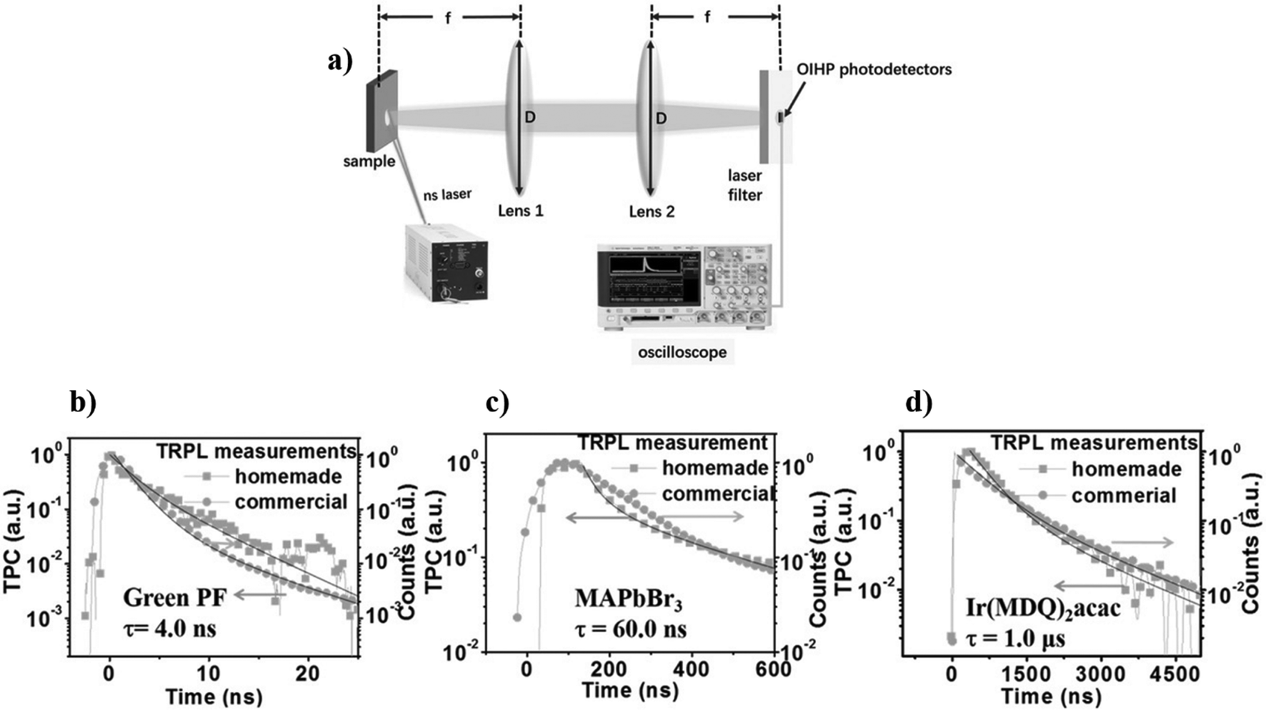
Towards realizing the commercial applications of self-driven PD based on OLHP, the work of Shen et al. can be considered as one of the most significant contributions. The authors demonstrated a homemade time-resolved photoluminescence (TRPL) system (Fig. 1a) facilitated by an ultrafast OLHP PD with the configuration of indium tin oxide (ITO)/poly(bis(4-phenyl)(2,4,6-trimethylphenyl)amine) (PTAA)/MAPbI3/C60/2,9-dimethyl-4,7-diphenyl-1,10-phenanthroline (BCP)/copper (Cu).59 The device area dependent sub-nanosecond response time (0.95 ns for 0.04 mm2 device area) of the PD enabled the detection of the photoluminescence lifetime for typical organic and hybrid materials, ranging from several nanoseconds to microseconds (Fig. 1b–d). In a recent work, Shan et al. presented a bifunctional light-emitting/detecting LiFi (light fidelity) fiber utilizing perovskite QDs.60 The authors capitalized on the small exciton binding energy and high carrier mobility of the all-inorganic perovskite QDs (CsPbBr3) to successfully integrate electroluminescence with narrow emission (∼19 nm) and photodetection in a single fiber. The flexible assembly exhibited green colored luminance of ∼100 cd m−2 at 7 V after being subjected to multiple bending cycles and the corresponding current efficiency was 1.67 cd A−1. The band bending in the space charge region at the interface between the perovskite QDs and the transport layers (due to differences in the Fermi levels) enabled a zero-bias operation of the PD with an on/off ratio of 1.5. OLHP QDs can potentially be utilized based on a similar principle for bi-functional devices. A major challenge that hinders the commercial viability of OLHP PDs (and other devices) is their instability in air and under ambient conditions. OLHP material rapidly degrades and decomposes in the presence of oxygen and moisture. Furthermore, electric field induced ion migration primarily across the perovskite grain boundaries further enhances material degradation, eventually worsening the optoelectronic properties.61 However, at the same time, the C-AFM and PC-AFM studies carried out by Li et al. in MAPbI3/CdS heterojunction PD indicated that a short transport distance at the grain boundaries acted as preferential spots of charge carrier transportation and exciton separation.62 The study of the photoelectric mechanism at the nanoscale showed that higher photocurrent values are observed at the grain edges. This offers the potential of grain boundary engineering towards fine-tuning the overall device performance. The fabricated PD exhibited a high current on/off ratio of ∼1.13 × 10⁵, detectivity of ∼9.79 × 10¹⁰ Jones, and PCE of up to ∼10.05%. Table 1 summarizes the heterojunction based self-powered OLHP PDs and their associated key figures of merit.
 |
| | Fig. 1 Homemade time-resolved photoluminescence lifetime (TRPL) detection system with OLHP PD: (a) layout of the TRPL system. The N2 ns laser acted as an excitation source for illuminating the sample from a small angle located at the focus position of Lens 1. The OLHP photodetector receives photoluminescence from the sample once redirected by Lens 2. A filter was incorporated to filter the laser scattering emission. A 1 GHz oscilloscope with a 50 Ω input resistance was connected to the PD to record the transient photocurrent curves. PL decay curves measured by homemade and commercial TRPL systems for (b) green polyfluorene (4.0 ns), (c) MAPbBr3 single crystal (60.0 ns) and (d) bis(2-methyldibenzo[f,h]quinoxaline) (acetylacetonate) iridium(III) (1.0 μs). The solid line is representative of exponential fitting to the data. Reproduced with permission from Shen et al., Adv. Mater., 28, 10794–10800.59 © 2016 Wiley-VCH Verlag GmbH & Co. KGaA, Weinheim. | |
Table 1 Summary of the p–i–n/n–i–p heterojunction based OLHP self-driven PDs and their device characteristics
| Device architecture |
Operating wavelength |
Responsivity |
Detectivity (Jones) |
Light switching ratio |
Response speed (rise/fall time) |
Ref. |
| FTO/ZnO/MAPbI3/Spiro-OMeTAD/Cu |
325 nm |
26.7 mA W−1 |
4.0 × 10¹⁰ |
|
53/63 μs |
49
|
| FTO/ZnO NR/MAPbI3/MoO3/Au |
500 nm |
24.3 A W−1 |
3.56 × 10¹⁴ |
|
0.7/0.6 s |
50
|
| FTO/ZnO/MAPbI3/MoO3/Au |
380 nm |
48 mA W−1 |
4.5 × 10¹¹ |
1400 |
14/12 ms |
51
|
| FTO/Ga3+ doped ZnO NR/MAPbI3/MoO3/Au |
490 nm |
0.3 A W−1 |
1.3 × 10¹² |
∼2.5 × 10³ |
<2/<2 ms |
52
|
| FTO/ZnO/MgO/MAPbI3/C |
473 nm |
5.9 × 10⁻² A W−1 |
1.5 × 10¹² |
7.0 × 10⁴ |
0.63/1.6 ms |
53
|
| ITO/MAPbI3:CuSCN/PCBM/BCP/Ag |
685 nm |
0.37 A W−1 |
1.06 × 10¹² |
|
5.02/5.50 μs |
54
|
| FTO/C60/MAPbI3/GaN |
500 nm |
0.198 A W−1 |
7.96 × 10¹² |
>5000 |
0.45/0.63 s |
55
|
| FTO/PEDOT:PSS + Ag NPs/CH3NH3PbI3/Al |
400 nm |
0.25 A W−1 |
1.53 × 10¹¹ |
|
110/72 ms |
56
|
| Al/BCP/PCBM/MAPbI3:GQDs/PEDOT: GQDs/TFSA-GR |
430 nm |
0.435 A W−1 |
8.7 × 10¹² |
|
0.56/0.96 μs |
57
|
| Planar Si/Si-NPA/MAPbI3/ZnO |
780 nm |
8.13 mA W−1 |
0.974 × 10¹³ |
0.82 × 10⁵ |
253.3/230.4 μs |
58
|
| ITO/PTAA/MAPbI3/C60/BCP/Cu |
680/700 nm |
0.47 A W−1 (−0.1 V) |
7.8 × 10¹² (−0.1 V) |
|
0.95 ns |
59
|
| ITO/CdS/MAPbI3/Au |
730 nm |
0.43 A W−1 |
2.3 × 10¹¹ |
1.13 × 10⁵ |
3.2/9.6 ms |
62
|
Although the p–n junctions have been widely applied in the fabrication of OLHP based self-driven PDs, little attention has been paid to the formation of the p–n homojunction within OLHP. Pang et al. stressed that the transport layers are optional in perovskite-based optoelectronic devices and claimed that the intrinsic light-induced self-poling ability in the perovskite could drive a Pt/CH3NH3PbI3/SiO2/Si/Al configured PD.63 The researchers through series of experiments ruled out the possibility of the observed self-powered characteristics being driven by the Schottky junction or poling of the device (by applying an external bias for a short duration before recording the device characteristics at 0 V). The authors hypothesized that under illumination, a built-in electric field was generated as positive ions/vacancies accumulated at the perovskite/SiO2 interface and negative ions/vacancies accumulated at the perovskite/Pt interface, owing to band bending in the asymmetric device. Under the influence of the built-in electric field, the photogenerated charge carriers drifted to their respective counter electrodes. While the holes were collected by the Pt electrode, the electrons traversed through the SiO2 film and were collected by the Al electrode by the ion trap-assisted emission mechanism (Frenkel–Poole emission). By contrast, under the dark conditions, SiO2 effectively acted as an insulating layer and functioned as a barrier layer for carriers, leading to ultralow dark currents. The detectivity of the fabricated self-powered PD was measured to be 8.8 × 10¹⁰ Jones with a high on/off ratio of 105 at 0 V. In a separate work, Ren et al. deliberately transformed the top surface of the p-type perovskite (MA+ rich and Pb2+ deficient stoichiometry) to n-type via bombarding with Ar+ ions leading to the formation of a p–n homojunction within the perovskite layer.64 The resultant built-in field in the perovskite promoted the separation and transport of photo-induced carriers without any external bias. The Ar+ ion bombarding facilitated MAPbI3 p–n homojunction PD exhibited an increase by one order of magnitude in the on/off ratio at 532 nm in comparison to the pristine MAPbI3 device.
1.2 Schottky junction-based PDs
A typical PD assembly incorporating a photosensitive semiconducting material with two ohmic metal contacts requires an external bias to drive the separation of the photogenerated electron–hole pairs. However, if one of the Ohmic contacts is replaced by a Schottky barrier contact, the built-in electrical field at that interface can lead to the separation of the photogenerated charge carriers. Unlike PDs with Ohmic contacts, the Schottky junction PDs, therefore, offer the ability to detect light irradiation without an external power supply and with high sensitivity and response speed complemented by the low dark currents. Multiple reports demonstrating the Schottky junction facilitated self-driven PDs are found in the literature. As a seminal work, the Schottky junction photodiode of the ITO/MAPbI3/Au vertical heterostructure assembly presented by Pandey et al. exhibited a photosensitivity of 1.33 × 10² with the rise time and decay time of 91 and 101 ms, respectively.65 Subsequently, several important works on high-detectivity and low-noise perovskite photodiodes were reported by different research groups. The ultrahigh mobility and conductivity of multilayer graphene and its ability to form a Schottky barrier with TiO2 were combined with the high yield photocarrier transport and strong broadband light absorption capability (260–900 nm) of CH3NH3PbI3, by Li et al.66 Both graphene and perovskite act as ambipolar materials and therefore, depending on the inherent Schottky field, electrons could be transferred vertically from perovskite to TiO2via the underlying graphene while the remnant holes remaining in the graphene were transferred horizontally and collected in a separate FTO electrode. The self-driven PD (FTO/TiO2–Graphene/MAPbI3/PTAA) demonstrated a high responsivity (∼0.375 A W−1) and specific detectivity (∼1011 Jones) and an excellent on/off ratio of 4 × 10⁶ in comparison to the commonly used Au–perovskite–Au configuration. The protection by the top PTAA layer enabled negligible decay in the performance of the PD despite storage under ambient conditions for 20 days and stability over 1000 cycles of operation.
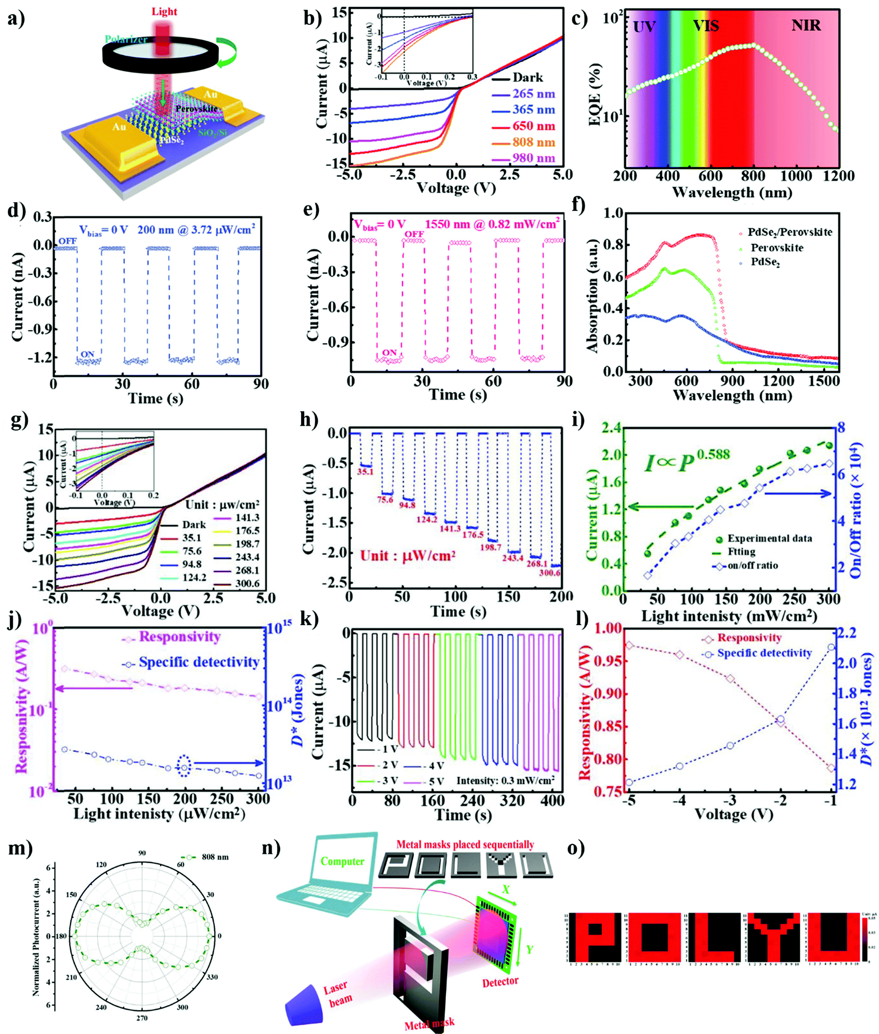
Other than graphene, 2D transition-metal dichalcogenides (TMDs) are being extensively researched for a wide array of potential applications, including optoelectronics, biosensors, and piezoelectricity.67–72 As a typical TMD material, MoS2 has suitable band levels and excellent charge transport properties, thus, is well suited to construct PDs based on the Schottky effect.73 Bai et al. were amongst the first ones to use single-layer MoS2 and MAPbI3 perovskite heterojunction in a vertically configured PD.74 At a light intensity of 0.7 mW cm−2, the self-powered PD exhibits a responsivity of 60 mA W−1 with an inverse relation to power density. Zeng et al. combined multi-layered PdSe2, another TMD material, with FA1−xCsxPbI3 perovskite to achieve a Schottky junction empowered fast self-driven PD with broad spectral sensitivity (200–1550 nm).75Fig. 2a provides the schematic illustration and Fig. 2b–l represents the optoelectronic response of the PdSe2/perovskite Schottky junction PD device. The high carrier mobility of PdSe2 and reduced surface defects at the TMD/perovskite interface enabled the Schottky junction-based PdSe2/perovskite PD to exhibit a large on/off ratio of ∼104, a high responsivity of 313 mA W−1 (Fig. 2j and l), a specific detectivity of ∼1013 Jones (Fig. 2l), and rapid response speeds of 3.5/4 μs. Moreover, the device exhibited sensitivity to polarized light, with a polarization sensitivity of 6.04 (Fig. 2m). To explore the infrared image sensing ability of the fabricated PD, homemade masks in the shape of alphabets such as P, O, L, Y, and U were placed between the laser illumination and the device as seen in Fig. 2n. The authors were then able to generate a 2D contrast mapping profile by plotting the dark current and photocurrent of the PD, at each pixel. Since the pixel illuminated by an 808 nm light demonstrated a considerable photocurrent of ∼0.05 μA, while the rest of the area displayed negligible dark currents, the authors were able to establish that the Cs-doped FAPbI3 PD could effectively resolve images under infrared illumination (Fig. 2o).
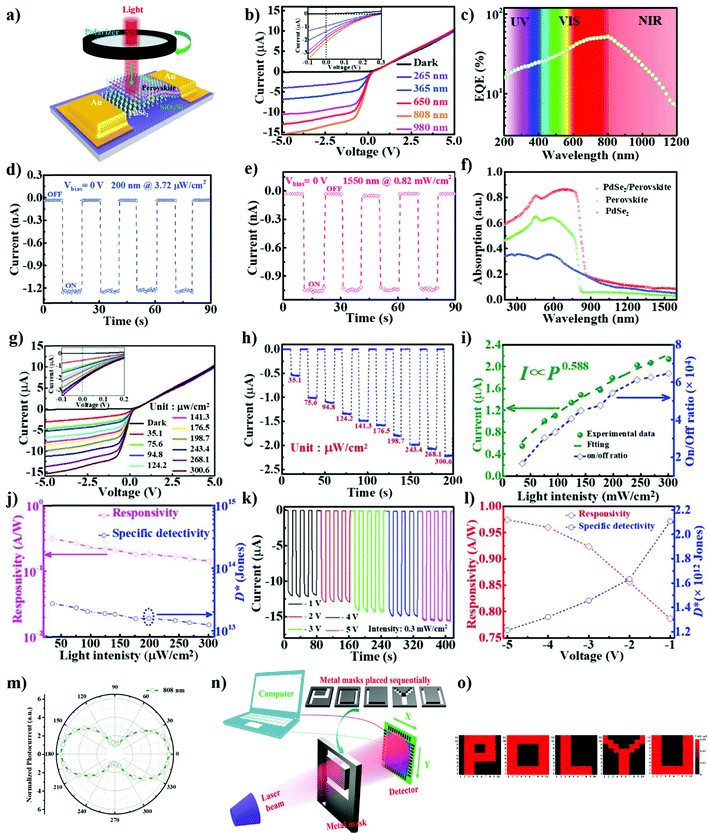 |
| | Fig. 2 Schematic illustration and optoelectronic measurement of the PdSe2/perovskite Schottky junction PD: (a) schematic of polarized detection device based on PdSe2/perovskite. (b) I–V curve in dark and under illumination with different lights. (c) Wavelength-dependent EQE at 0 V. Spectral photoresponse in the self-powered mode under (d) 200 nm (3.72 μW cm−2) and (e) 1550 nm (0.82 mW cm−2) light illuminations. (f) Independent UV-Vis absorption spectrum of PdSe2, perovskite, and PdSe2/MAPbI3. (g) I–V curves of PD in dark and under an 808 nm light irradiation with different intensities. (h) Time-dependent photocurrent under an 808 nm light illumination with different light intensities. (i) Photocurrent and on/off ratio as a function of light intensity at zero bias. (j) Responsivity and detectivity as a function of incident power intensity. (k) Time-dependent photocurrent at reverse bias under an 808 nm light illumination (0.3 mW cm−2). (l) Responsivity and detectivity as a function of operating bias voltage (0.3 mW cm−2). (m) Evolution of photocurrent as a function of different polarized angles. (n) Homemade experimental setup to realize detection ability of PdSe2/OLHP PD for NIR imaging sensing. (o) The corresponding 2D current mapping of characters “P,” “O,” “L,” “Y,” and “U” produced by an 808 nm laser. Reproduced from Zeng et al., Adv. Sci., 6, 1901134.75 © 2019 WILEY-VCH Verlag GmbH & Co. KGaA, Weinheim. | |
1.3 Ferroelectric and polarization effect based PDs
Ferroelectrics present a promising alternative for generating power in single-phase homogeneous materials by using polarization to trigger light detection. However, the presence of the ferroelectric polarization effect in OLHP is still debatable.76–81 Saraf et al. discussed the interplay between the polarization effect and ion migration as a function of poling conditions in MAPbI3 based PD (Fig. 3a).82 The work supported the presence of ferroelectric effect in MAPbI3 as the PD poled under air and illumination lead to a ferroelectric dominated response, while poling under N2 and dark conditions leads to ion migration effects resulting in the formation of a p–n homojunction which is signified by a reversal in signs for open-circuit voltage (Voc) and short circuit current (Isc) as observed in Fig. 3b–e. To obtain a stable response, poling was done under a small external bias applied across the Au/MAPbI3/Au configuration in air and under illumination for a short duration of 10 minutes. The poled device could then operate without requiring an external power supply for the next 2 days. Besides, the authors adopted an additive engineering strategy of integrating polystyrene (PS) in the MAPbI3 films to enhance their stability. The PS–MAPbI3 based planar configuration PD device illustrated an impressive performance stability of >80% post 20 days. On the other hand, the pristine MAPbI3 counterpart device suffered from a 70–85% performance decay within 4 days of operation under similar ambient conditions. The monolith PD achieved a photoresponsivity of more than 0.61 A W−1 and a detectivity of 1.5 × 10¹³ Jones under such self-powered operation. Recently, utilizing the same device architecture and self-powered mechanism, Mathur et al., unveiled the nanoscale tri-layer architecture of the polymer-perovskite (PS–MAPbI3) films in which the polymer forms a thin layer at the top and bottom interfaces while the perovskite forms bulk of the interlayer.83 It was observed that the viscosity of the polymer chains, directly dependent on the molecular weight (Mw) of the integrated polymer, is critical in determining the chain mobility and drives the rearrangement of the polymer chains across the perovskite film. Not only does the inclusion of varying Mw of PS (2.5, 11, 35, 61, 105, and 190 kDa) modulate the crystallization kinetics but the insulating nature of the polymer chains also affects the charge transport. The presence of PS chains, predominantly at the grain boundaries reduces ion mobility and hence leads to reduced dark currents and ionic currents. Overall, the inclusion of intermediate Mw PS chains of 35 kDa led to optimized electro-optical properties with enhanced stability in the corresponding self-powered PD. Specifically, a 3-fold enhancement in Isc (96.6 nA) and Voc (162.5 mV) was observed for 35 kDa PS–MAPbI3 PD in comparison to pristine MAPbI3 (31.1 nA and 52.3 mV, respectively).
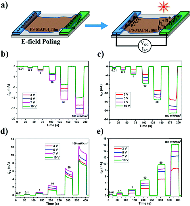 |
| | Fig. 3 Device architecture and photoresponse after poling of MAPbI3 based PD in different environments: (a) schematic diagram of the lateral self-powered PD and the effect of electric field poling leading to Voc and Isc response at zero bias. The Isc response at 0 V from (b) MAPbI3, and (c) PS–MAPbI3 devices to various light illumination intensities, post poling at different voltages for 10 min in air and under light illumination (1.0 sun). The Isc response at zero bias from (d) MAPbI3 and (e) PS–MAPbI3-based PDs at various light intensities after poling at different voltages under N2 and dark. Reprinted with permission from R. Saraf and V. Maheshwari, ACS Appl. Mater. Interfaces, 10, 21066–21072.82 Copyright © 2018 American Chemical Society. | |
Irrespective of the debatable existence of ferroelectric polarization in perovskites, incorporation of an additional layer of a ferroelectric material in the perovskite PD architecture can enhance the built-in electric field leading to improved charge extraction. A report demonstrating polarization induced internal electric field in a perovskite-based device appeared in 2018 where Cao et al. integrated ferroelectric SrTiO3 (STO) to serve as an interlayer in a sandwich structure of FTO/STO/MAPbI3/Spiro-OMeTAD/Ag.84 The polarized STO layer provides a built-in potential and promotes downward band bending, helping to separate and transport charge carriers generated in MAPbI3 upon illumination. Upon optimization of the STO layer density, the photocurrent was enhanced up to 0.956 mA with response speeds of 0.3 s (rise time) and <0.1 s (decay time) at 0 V in a PD positively poled at 1 V for 5 min. However, unlike the report of Saraf et al., there was an obvious decrease in photoresponse upon exposure to air for 24 h. The substantial performance decay can be attributed to the decomposition and degradation of the OLHP active layer which is indicative of the limited stability of the fabricated PD. The authors later demonstrated a poling induced self-driven bulk heterojunction PD. This research involved the integration of another ferroelectric material P(VDF-TrFE) to enhance the strength of the ferroelectric field of the perovskite layer, facilitating better separation of the photogenerated charge carriers.85 The corresponding PD exhibited high responsivity (20 mA W−1), large detectivity (1.4 × 10¹³ Jones), and fast response speed (92/193 μs) at the wavelength of 650 nm. Later, the group extended the same composite assembly in the form of a nanowire array via an imprinting method assisted by commercially available digital versatile discs (DVD).86 The resultant flexible hybrid device on the PEN substrate exhibited high detectivity (7.3 × 10¹² Jones), fast response time (88/154 μs) at zero bias, and impressive mechanical stability through bending up to 180 degrees.
1.4 Triboelectric nanogenerator (TENG) based PDs
Triboelectric nanogenerators (TENGs) can act as an efficient driving source for harvesting mechanical energy to power devices such as PDs. When a physical contact occurs at the interface of two dissimilar materials, typically opposite triboelectric charges are created on the two surfaces. A mechanical motion can then induce an inherent electric potential difference capable of driving electrons back and forth between the electrodes. Su et al. fabricated a UV-Visible broad range PD based on the dual properties of MAPbI3: photoconductivity and surface triboelectric charge density.87 An oscillating Voc was generated upon the top copper electrode periodically getting into contact with the underlying perovskite layer. Upon photoexcitation, electrons from the photogenerated electron–hole pair got quickly captured by the mesoporous TiO2 layer, while holes tend to partially neutralize the negative triboelectric charges present on the surface leading to an instantaneous decrease in surface charge density. The corresponding device demonstrated a responsivity of 7.5 V W−1 with a response time of <80 ms. Later, Hsiao et al. demonstrated a similar TENG assisted perovskite PD that could generate photo response upon bending of the flexible assembly.88 Guo et al. designed a self-powered organic optical communication system (SOCS).89 This system was composed of organic light-emitting diode (OLED) driven by triboelectric nanogenerators (TENGs) and perovskite PD. In this SOCS, the mechanical signals were converted into light by the OLED and then transferred to voltage signals by the perovskite PD. The combination of TENG with OLED exhibiting an emission peak at ∼524 nm served as a light emitter in the robotic hand, while PD served as the output voltage of SOCS with a maximum current transfer ratio of 30%. The output voltage of SOCS was modified by the different mechanical actions of the robotic hand which could be used to transmit the information on human–machine interaction.
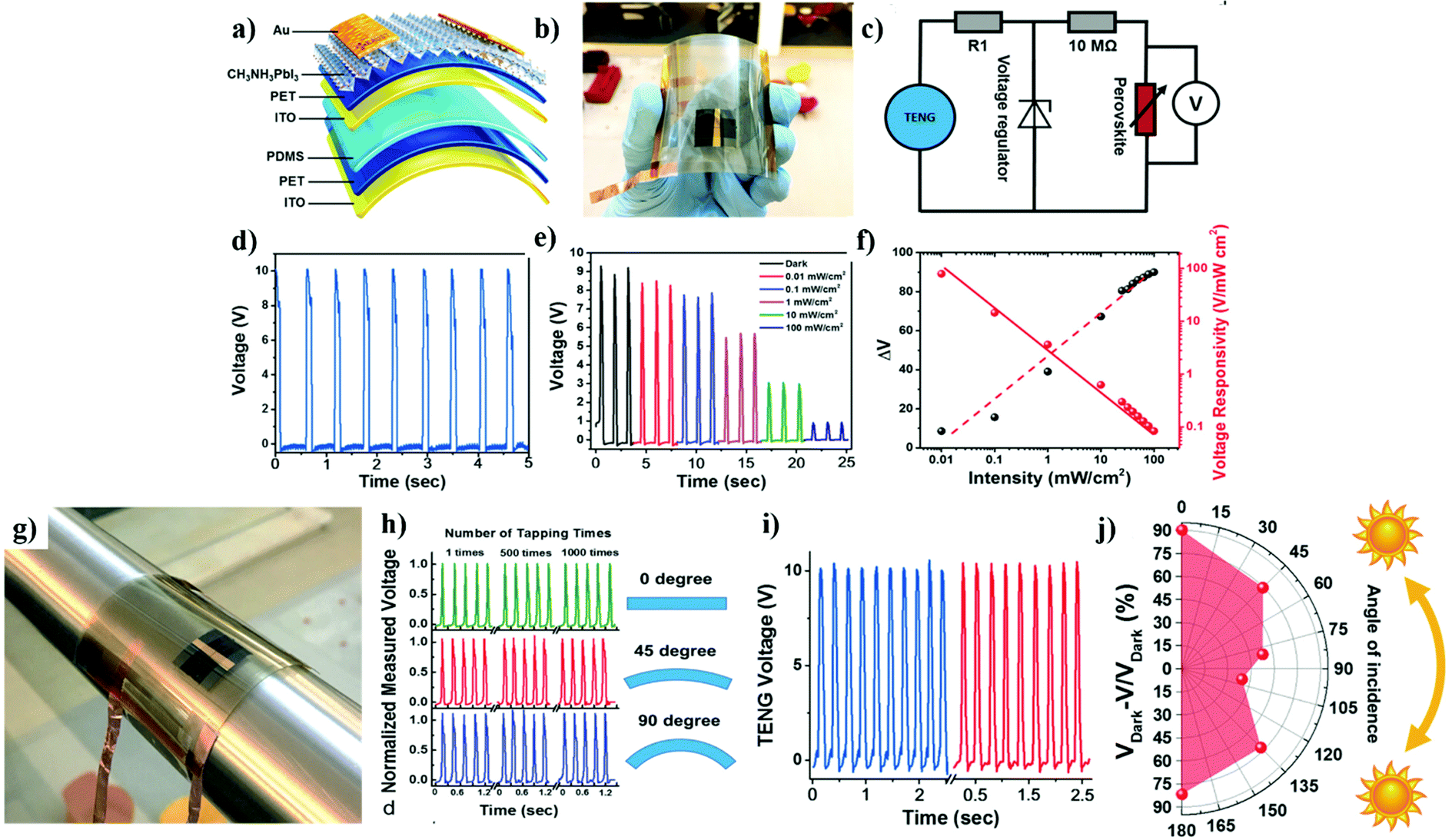
One of the biggest limitations of conventional TENG-powered devices is their dependency on motion actuators as a power source which are prone to fluctuations due to variation in the surrounding conditions, severely hindering the accuracy of photodetection. The self-powered PD reported in work by Leung et al. aimed at mitigating this issue by excluding mechanical pressure being applied to the TENG (Fig. 4a–c).90 The PD instead utilized the voltage regulated circuit containing a resistor and a Zener diode, which enabled uniform photodetection characteristics irrespective of irregular motion, such as human finger tapping (Fig. 4d). The fundamental principle comprised perovskite acting as a variable resistor dependent on the incident light intensity. The voltage in the photosensitive layer followed an inverse relation with light intensity owing to a decrease in resistivity by the photogenerated carriers (Fig. 4e and f). The flexible and transparent polymer architecture of the PD empowered a stable device performance after 1000 bending cycles and photosensitivity at 360 degrees of illumination (Fig. 4j). The self-powered PD exhibited an impressive maximum voltage responsivity of 79.4 V mW−1 cm−2 and a ∼90% change in voltage at an incident light intensity of 100 mW cm−2 compared to the voltage obtained in dark.
 |
| | Fig. 4 Device structure, optical image, circuit diagram, and electro-optical measurements of the TENG powered flexible PD: (a) schematic illustration of the self-powered flexible PD. (b) Optical image demonstrating high transparency and flexibility of the as-fabricated OLHP PD. (c) Equivalent circuit diagram. (d) Regulated voltage output of the TENG driven by finger tapping, corresponding to voltage spikes. (e) Light intensity dependent voltage response of the PD. (f) The change in the measured voltage (ΔV) and voltage responsivity of the device at different light intensities. (g) Photograph of a perovskite PD attached to a curved surface. (h) The self-powered perovskite PD features stable performance upon repeated bending at various angles of curvature. (i) The TENG output by two different people, demonstrating the highly regulated TENG voltage output attributing to the regulating circuit. (j) Change in voltage response at various angles of incident light. Reproduced with permission from Leung et al., Adv. Mater., 30, 1704611.90 © 2018 WILEY-VCH Verlag GmbH & Co. KGaA, Weinheim. | |
1.5 Common strategies to enhance the figures of merit of OLHP PDs
Table 2 summarizes a representative list of OLHP based PDs where various strategies such as crystal structure engineering, modulation of the synthesis procedure, and broadening of the spectral range were employed to enhance device characteristics.
Table 2 Summary of OLHP based self-driven PDs where various strategies were utilized to improve the key device characteristics
| Strategy |
Device architecture |
Self-powered operating principle |
Operating wavelength |
Responsivity |
Detectivity (Jones) |
Light switching ratio |
Response speed (rise/fall time) |
Ref. |
| Crystallite structure engineering |
Al/CH3NH3PbI3/Cu |
Triboelectricity |
white light |
196 V (mW cm−2)−1 |
|
|
<0.2/<0.2 s (4 V) |
92
|
| Au/CH3NH3PbI3/Al |
Schottky junction |
808 nm |
0.24 A W−1 |
|
20 |
71/112 μs |
93
|
| FTO/MAPbBr3/MAPbIxBr3−x/Au |
Heterojunction |
450 nm |
11.5 mA W−1 |
|
|
2.3/2.76 s |
94
|
| ITO/SnO2/MAPb(IxBr1−x)3 MC/C |
Heterojunction |
|
0.26 A W−1 |
7.01 × 10¹¹ |
2 × 10⁵ |
80/580 μs |
95
|
| ITO/MAPbI3 NCs/Ag |
Schottky junction |
808 nm |
1.42 A W−1 |
1.77 × 10¹³ |
932 |
279/341 ms |
96
|
| Modulation of synthesis procedure |
FTO/TiO2/CH3NH3PbI3/Spiro-OMeTAD/Ag |
Heterojunction |
650 nm |
0.55 A W−1 |
∼1012 |
∼104 |
460/940 ns |
97
|
| FTO/TiO2/Cs0.05FA0.16MA0.79PbI2.7Br0.3/Spiro-OMeTAD/Ag |
Heterojunction |
|
|
|
1.73 × 10³ |
12.4/26.4 μs |
98
|
| FTO/NiOx/MAPbI3−xClx//PCBM/Au |
Heterojunction |
632 nm |
112.9 A W−1 |
3.53 × 10¹⁴ |
|
0.23/0.38 s |
99
|
| FTO/TiO2/MAPbI3−xBrx/PCBM/Au |
Heterojunction |
632 nm |
45 A W−1 |
1.15 × 10¹⁴ |
|
0.24/0.38 s |
100
|
| FTO/TiO2/CH3NH3Pb0.99Bi0.01I3/Au |
Heterojunction |
Visible light |
1 × 10⁻⁴ A W−1 |
|
|
902/762 ms |
101
|
| Spectral range broadening |
ITO/PEDOT:PSS/(FASnI3)0.6(MAPbI3)0.4/C60/BCP/Ag |
Heterojunction |
900 nm |
0.4 A W−1 (−0.2 V) |
1.1 × 10¹² (−0.2 V) |
|
6.9/9.1 μs |
103
|
| Si/MPS/metal/MoO3/PEDOT:PSS/Sn-rich binary perovskite/PC61BM/ZrAcac/transparent thin metal film/MoO3 |
Heterojunction |
940 nm |
0.2 A W−1 |
∼1011 |
|
90 ns/2.27 μs |
104
|
| FTO/SnO2/KMAPbClxBr3−x/Spiro-OMeTAD/Au |
Heterojunction |
|
|
|
|
∼71 ns |
105
|
| MAPbI3−xClx/TiO2/Si |
Heterojunction |
800 nm |
870 mA W−1 (+4 V) |
6 × 10¹² (+4 V) |
116 |
50/150 ms |
106
|
1.5.1 Crystallite structure engineering.
Several attempts have been made to improve the figures of merit for the perovskite based self-powered PDs by engineering the crystallite structure and composition. Perovskite single-crystal materials exhibit high carrier mobility (>100 cm2 V−1 s−1), long diffusion lengths, low trap-state densities (∼1010 cm−3), and high absorption coefficients as compared to their polycrystalline counterparts which are beneficial for the realization of high-performance PDs.91 Fang et al. published a pioneering report on single crystal based planar PD driven by a drum shaped assembly of two DVDs functioning as a triboelectric nanogenerator.92 The nano-patterned polycarbonate substrate face of DVD was used as one of the friction layers of the TENG. An Al conductive tape was applied on the reverse side of the DVD to serve as an electrode. A sanded Cu conductive tape pasted on another DVD acted as the opposite friction layer. Multiple pieces of polyethylene terephthalate (PET) were used to connect the two friction layers face-to-face, resulting in a drum shaped TENG with the single crystal perovskite sandwiched in between. Fig. 5a represents the equivalent circuit of the self-powered PD system in which OLHP single crystal served as a TENG. The self-powered device yielded up to 200 V and 55 mA upon being subjected to finger tapping (Fig. 5b and c). The crude yet simplistic approach enabled large responsivity of 196 V (mW cm−2)−1 with a wide detection range from 10 to 100 mW cm−2 (Fig. 5d–f). Capitalizing on the advantage of higher current saturation density offered by asymmetric metal contacts (Au–Al), Ding et al. fabricated a facile Schottky junction (Au/CH3NH3PbI3/Al) enabled PD with an inherent built-in field.93 The single crystal MAPbI3 device exhibited responsivity as high as 0.24 A W−1 and a fast rise time and decay time of 71 μs and 112 μs, respectively. Cao et al. fabricated a MAPbBr3/MAPbIxBr3−x core–shell heterojunction-based PD.94 The strong local electric field arising from band bending at the MAPbBr3/MAPbIxBr3−x heterojunction facilitated efficient exciton dissociation and suppressed charge recombination. Under the influence of the inherent field, the electrons were injected into the CH3NH3PbIxBr3−x shell while the holes were transferred to the MAPbBr3 single crystal core, enabling photoresponse at zero bias. The self-powered PD exhibited a responsivity of 11.5 mA W−1 and a quantum efficiency of 3.17%, both being higher than the respective values observed for the MAPbBr3 single crystal counterpart. Despite the advantages offered by single crystals, fabricating solution processed large-area single crystal films with controllable thickness is still a major challenge. Pan et al. instead proposed utilization of perovskite microcrystals (MCs) that possess advantages similar to single crystal perovskite (low defect state density and high carrier mobility) with the ability of tuning film thickness by tweaking precursor solution concentration and antisolvent content.95 The authors fabricated a HTL-free ITO/SnO2/MAPb(IxBr1−x)3 MC film/carbon heterojunction assembly with adjustable band gap and the ability to operate without external bias. With the decrease in the iodide content (x) in the perovskite precursor solution, the absorption edge of the MAPb(IxBr1−x)3 MC film gradually shifted to the blue region with the corresponding bandgap increasing from 1.53 eV of MAPbI3 to 2.22 eV of MAPbBr3. The perovskite MC films with optimized thickness led to an on/off ratio of 2 × 10⁵, a responsivity of 0.26 A W−1, a specific detectivity of 7.01 × 10¹¹ Jones, a rise/fall time of 80/580 ms, and a linear dynamic range of 107 dB. Furthermore, the MC based PDs show negligible attenuation upon continuous exposure to light and air for 30 minutes and an overall 16% decrease in performance when stored in air for a month. In a recent work, Perumal et al. presented an ultrasonication based ligand-assisted reprecipitation (LARP) technique to produce air-stable MAPbI3 nanocrystals. The MAPbI3 nanocrystals were spray-casted or drop-casted over patterned asymmetric ITO-Ag electrodes to obtain a self-powered PD.96 The optimized PD showed a responsivity of 1.42 A W−1 and a specific detectivity of 1.77 × 10¹³ Jones under an 808 nm light illumination at zero bias, and maintained 90% performance over 1 month.
 |
| | Fig. 5 Circuit diagram and optoelectronic characteristics of the triboelectric effect driven MAPbI3 single crystal PD: (a) the equivalent circuit of the self-powered PD nanosystem where Dz represents a commercial Zener diode. Measured (b) Voc and (c) Isc response from the TENG during the periodical finger tapping in the forward connection. The measured voltage drop across the CH3NH3PbI3 single crystal photodetector in (d) dark and under (e) various illumination intensities. (f) Voltage change (defined as (V0 − V)/V0) and photoresponsivity of the nanosystem as a function of illumination intensity. Reproduced from ref. 92 with permission from The Royal Society of Chemistry. | |
1.5.2 Synthesis strategy.
The quality and compactness of the perovskite film strongly determine its inherent stability and overall device performance. Developing and improvising fabrication techniques that allow precise control over the quality, morphology, composition, and crystallinity of the perovskite films are thus crucial. Tong et al. explored a lower temperature range of 90–150 °C and a fast chemical vapor deposition (LF-CVD) route to synthesize compact uniform and smooth perovskite films.97 The expansive gas–solid reaction of perovskite crystallites with optimal annealing at 120 °C for 30 min led to the restriction of pinholes to grain boundaries while maintaining the integrity of the thin film. Simultaneously, the accumulated strain at the colliding grain boundary interfaces led to selective evaporation of MAI leaving behind a thin layer of PbI2 at the grain boundaries. The authors claimed that the wider bandgap of PbI2 in comparison to perovskite provided good passivation at the grain boundaries and helped reduce local recombination centres and block local leakage current. The corresponding self-driven vertically configured FTO/TiO2/perovskite/Spiro-OMeTAD/Ag PD device exhibited a detectivity of ∼1012 Jones, a responsivity of 0.55 A W−1 with fast rise time and fall time of 460 ns and 640 ns, respectively (Fig. 6). The two-month air-stable PD also showcased a wide 3 dB bandwidth up to 0.9 MHz. Adams et al. proposed to alleviate the repeatability and scalability challenges associated with the typical anti-solvent drip method used in the synthesis of perovskite films by using the anti-solvent bath method with improvised annealing.98 A low-temperature fabrication method was employed to obtain large grain sized, Cs/FA/MA triple cation perovskite PDs with a low dark current, >103 on/off ratio, and a rise time of 12.4 μs. Pammi et al. fabricated high-quality large grain size rich polycrystalline thin films of MAPbI3−xClx99 and MAPbI3−xBrx100via the chemical vapor deposition (CVD) method. The corresponding PDs exhibited an impressive figure of merit. More importantly, after 500 h of illumination, the normalized responsivity reduced by 25% and 29% for the MAPbI3−xClx and MAPbI3−xBrx based PDs, respectively, in comparison to 62% in pristine MAPbI3 based PD, signifying the enhanced stability of the chlorine and bromine doped perovskite films. Sadhasivam et al. used CVD to deposit a crystalline layer of Pb0.99Bi0.01I2 over TiO2 nanoarrays which was later transformed to CH3NH3Pb0.99Bi0.01I3 by introducing methylamine iodide at distinct time intervals.101 The corresponding PD exhibited a responsivity of 10−4 A W−1 at 0 V.
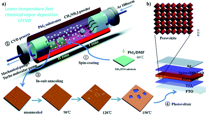 |
| | Fig. 6 Stepwise CVD fabrication process and multilayer structure of the perovskite device: (a) schematic illustration of the configuration of the two-temperature-zones furnace tube and the fabrication procedure of a lower temperature fast chemical vapor deposition process (LF-CVD) for synthesizing perovskite films. (b) The multilayer structure of the final perovskite photovoltaic detector. Reproduced from ref. 97 with permission from The Royal Society of Chemistry. | |
1.5.3 Broadening of the PD spectral range.
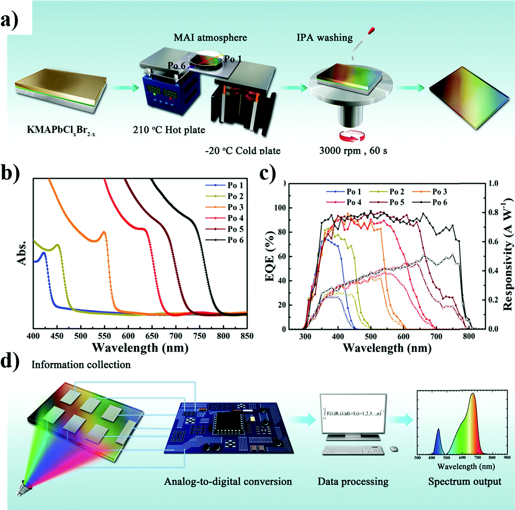
One of the limitations associated with perovskite-based PDs is their attenuated absorption capacity in the NIR range. To broaden the spectral range of the perovskite-based PDs, two approaches have been commonly adopted: (1) lowering the bandgap of perovskite by substituting cation or/and a halide moiety102 or (2) combining the perovskite layer with another narrow bandgap semiconductor. Wang et al. followed the first strategy of cation and halide substitution to fabricate a low bandgap (FASnI3)0.6(MAPbI3)0.4 perovskite-based PD with a broadband response extending from UV (300 nm) to NIR (1000 nm).103 The as-fabricated vertically configured ITO/PEDOT:PSS/(FASnI3)0.6(MAPbI3)0.4/C60/BCP/Ag device exhibited almost identical EQE spectra under 0 and −0.2 V, indicating its self-powered ability. The authors used C60 as a hole blocking layer and to passivate the surface charge traps, leading to a reduced leakage current under reverse bias. The thin BCP layer served as a cathode buffer layer to enhance the contact between the C60 layer and the Ag cathode. Zhu et al. illustrated a room-temperature strategy to manipulate the crystallization kinetics of Sn-rich binary perovskite films fabricated over a complementary metal–oxide–semiconductor (CMOS) compatible silicon substrate.104 The Pb–Sn mixed perovskites are considered promising narrow-bandgap materials offering the advantage of expanding the spectral response to the NIR region. However, compared to their Pb analogues, Sn-based perovskite precursors have a greater tendency to react and crystallize at room temperature, resulting in high surface roughness and severe pinholes in the corresponding films. By carrying out careful experimental and theoretical studies focused primarily on the timespan between the antisolvent washing process and the post-annealing treatment, the authors were able to control the density and location of the compact nanocrystals formed in the precursor films. Upon flash annealing, these compact nanocrystals coalesced into a smooth pin-hole free MASnxPb1−xI3 film with preferred orientation and reduced trap density. The corresponding self-powered devices with a carrier extraction layer/metal/Si substrate structure, achieved a high responsivity of 0.2 A W−1 at 940 nm, a large linear dynamic range of 100 dB, and a fast fall time of 2.27 μs. The authors also demonstrated a 6 × 6-pixel array based on the Sn rich binary perovskite films with excellent photocurrent uniformity. In another interesting work aimed at producing filter-free/spectrum sensitive PD, as illustrated in Fig. 7a, Sun et al. demonstrated in situ bandgap gradient within an array of KMAPbClxBr3−x absorber films when subjected to a temperature bridge across the integrated device.105 The integrated self-driven PD with a high spectral resolution (∼80 nm) (Fig. 7b and c) exhibited a rapid response time (∼71 ns) due to the influence of carrier concentration (Cl− vacancies) over interfacial capacitance while maintaining a maximum external quantum efficiency (EQE) of over 90%. Fig. 7d represents the schematic layout of the KMAPbClxBr3−x film-based spectrum detection system. On the other hand, following the second approach for enhancing the spectral response of perovskite-based PDs, Cao et al. combined a narrow bandgap n-Si wafer with an active layer of MAPbI3, spin-coated over a TiO2 interlayer to fabricate a trilayer hybrid PD.106 The TiO2 thickness dependent I–V rectification characteristics suggested the presence of a built-in electric field in the as-prepared PD and its ability to work under zero bias. Showcasing a broad spectral response up to 1150 nm, the PD exhibited a rise time and decay time of 50 and 150 ms, respectively.
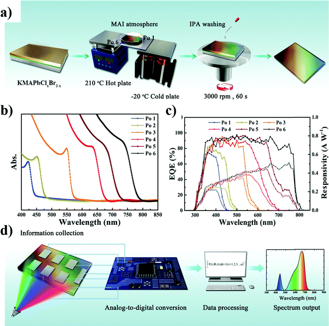 |
| | Fig. 7 Fabrication procedure and optical and electro-optical measurements of gradient perovskite film: (a) schematic diagram of the gradient perovskite absorber preparation process. (b) The absorption spectra of the gradient perovskite absorber with different positions. (c) The EQE spectra of the PD based on various absorber positions. (d) Schematic diagram of the final color/spectrum detection system. Reproduced with permission from Sun et al., Adv. Mater., 32, 1908108.105 © 2020 WILEY-VCH Verlag GmbH & Co. KGaA, Weinheim. | |
1.6 Flexible PDs
Compared with the traditional devices based on a rigid silicon substrate, flexible PDs have wider applications in the field of wearable and portable devices owing to their reduced weight and promising applications in healthcare, robotics, epidermal sensing, and so forth. Due to their low-temperature solution-processing and light absorption characteristics, perovskite thin films can serve as an optimal light-harvesting material in such applications. Among the initial works based on OLHP flexible PDs, Bao et al. demonstrated a flexible PD with poly(ethylene 2,6-naphthalate) (PEN)/Au NW serving as a transparent electrode.107 The peak EQE and responsivity of the device reached 60% and 314 mA W−1, respectively, with a 4.0 μs rise time and a 3.3 μs fall time. In another work, Sun et al. utilized a blend of CH3NH3PbI3 and Spiro-OMeTAD as a photosensitive material over low-cost carbon cloth, serving both as a substrate and a conducting electrode to fabricate a flexible PD.108 The solution processed device exhibited high detectivity and light responsivity, a large on/off ratio, and a broad-spectrum response to light ranging from UV (300 nm) to NIR (820 nm) at zero bias. The flexible PD exhibited a fast response speed and reproducible characteristics under white light irradiation after 80 bending cycles and showed photoresponse even at high bending angles such as 180°. The same group later reported a flexible PD based on a single fibre. Here, perovskite microcrystals were solution coated over a commercial carbon fibre with an intermediated thin layer of TiO2.109 A CuO nanowire–Cu2O compact layer grown over a flexible Cu fibre was double twisted over the perovskite-coated carbon fibre to function as a cathode while the carbon tape end of the parent fibre was utilized as an anode Fig. 8a represents the complete fabrication process and energy level diagram of the as-fabricated fibre PD. Under the self-powered mode, the flexible PD exhibited ultralow dark current (10−11 A) empowering high detectivity of up to 1013 Jones while the narrow bandgap of CuO enabled the broadening of the spectral response range from UV (350 nm) to NIR (1050 nm) (Fig. 8b–e). The device demonstrated a rapid response speed (<200 ms) and reproducible photoresponse characteristics after being subjected to 60 bending cycles. Another similar work reporting a flexible wire-shaped PD is from Adams et al.110 The research emphasized the predominance of Joule heating (direct conversion of electric energy to heat) over the conventional hot-plate heating method by allowing rapid heating or cooling of a substrate and thereby enabling a higher degree of control. The ohmic heating method allowed uniform temperature distribution across the thread-like carbon nanotube yarn (CNY) which, in turn, facilitated the deposition of a compact polycrystalline perovskite layer. The asymmetric top InGa and bottom CNY electrode contacts created a built-in potential sufficient to overcome the binding energy of photogenerated electron–hole pairs. The resultant PD had a responsivity of 10.2 A W−1 and a detectivity of 1.76 × 10¹¹ Jones with an on/off ratio of 45. Utilizing the anti-solvent crystallization technique, Lim et al. patterned an array of MAPbI3 nanoribbons over a variety of substrates including the flexible polyimide substrate.111 Dripping of nonpolar toluene facilitated the abrupt precipitation of perovskite grains and removal of residual perovskite precursor solvent confined within the hydrophobic trap of polymethyl methacrylate (PMMA) nanotemplate, leading to a directional growth of perovskite grains. The phase switching local hysteresis and amplitude butterfly loops, suggestive of the ferroelectric nature of MAPbI3, were observed during the characterization of the perovskite films. The authors hence argued that the ferroelectricity and anisotropic alignment of the hierarchical array of MAPbI3 nanoribbons led to the self-powered and polarization-sensitive optoelectronic response in the resultant flexible PD. One of the major challenges against the realization of optimum capabilities of the perovskite-based flexible PDs lies in the high-temperature treatment required for the carrier extraction layer during device fabrication. Wang et al. in their work focussed on low temperature (80 °C) processed In2S3 nanoflake film grown to effectively serve as the electron transport and hole blocking layer over the ITO/PEN substrate with MAPbI3 serving as a photosensitive layer.112 The resultant PD exhibited a broadband response up to the NIR range with responsivity up to 451 mA W−1 at 720 nm without any external power supply. The flexible device showed only a 15% loss of current with a bending radius up to 2.5 mm. Tian et al. demonstrated a relatively less researched, nested inverse opal structured (Cs0.05(FA0.85MA0.15)0.95Pb(I0.85Br0.15)3) perovskite-based flexible PD.113 The combined effect of improved light trapping and perovskite crystallinity enabled the self-driven device to exhibit a responsivity of 473 mA W−1 and a detectivity of 1.35 × 10¹³ Jones with reproducible photoresponse after 500 bending cycles. The PS template-assisted device fabrication enabled enhanced hydrophobicity across the device surface which in turn permitted the PD stored in an ambient environment to operate for over 16 days without significant decay in performance. Several other reports have appeared recently representing the increased attention being paid to flexible PDs. Shin et al. reported photodiode cum solar cell with identical configuration (TETRA-GR/MoS2/MAPbI3/PCBM/BCP/Al) utilizing bilayer MoS2 as the ETL and triethylenetetramine doped graphene (TETA-GR) as a transparent conductive electrode.114 The flexible PD maintained about 80% of its original responsivity even after 1000 bending tests at a radius of curvature of 4 mm. Later, the authors showcased the versatility of MoS2 by utilizing it instead as the HTL in a similar bifunctional flexible device but with an inverted p–i–n configuration.115 The flexible PD maintained ∼57% of its initial photocurrent after 3000 bending cycles at a curvature radius of 4 mm. More recently, Tao et al. demonstrated CH3NH3PbI3 NWs sandwiched between asymmetric Ni–Al electrodes on a flexible polyimide film.116 The formation of the metal/perovskite Schottky barrier at the interface of asymmetric Al (4.3 eV) and Ni (5.1 eV) electrodes led to a built-in electric field in the device which could effectively separate charge carriers. The corresponding self-powered device exhibited a responsivity of 0.227 A cm−2 at an incident light power of 1 × 10⁻⁸ W cm−2 and an on/off ratio of 147. Although appreciable developments have been made in the field of flexible self-powered PDs, it is worth considering that most of the reported PDs have small active areas and their optimum performance lasts only for few thousand cycles. Hence, besides optimizing the photosensitive perovskite layer to mitigate material degradation issues, a careful selection of suitable electrodes and substrates to facilitate large-area self-powered PDs with a stable long-term device operation is equally critical. In a recent work, Saraf et. al utilized Au–Pt gold nanoparticle chain-based electrodes on a flexible filter membrane to fabricate a porous Au–Pt/PS–MAPbI3/Au–Pt PD assembly.117 The flexible PD maintained 85% of its initial performance after 10![[thin space (1/6-em)]](https://www.rsc.org/images/entities/char_2009.gif) 000 bending cycles at 120°. The highly flexible nanoparticle chain electrodes can potentially be expanded to fabricate asymmetric contact to induce a built in electric field within the perovskite and obtain a self-powered PD. The key figures of merit and device configuration of OLHP based flexible PDs are presented in Table 3.
000 bending cycles at 120°. The highly flexible nanoparticle chain electrodes can potentially be expanded to fabricate asymmetric contact to induce a built in electric field within the perovskite and obtain a self-powered PD. The key figures of merit and device configuration of OLHP based flexible PDs are presented in Table 3.
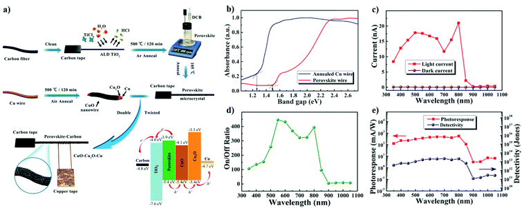 |
| | Fig. 8 Fabrication strategy and the electro-optical response of the perovskite-based fiber-shaped PD: (a) schematic illustration of the fabrication process and energy level diagram of the fiber-shaped PD. (b) Absorption spectrum of perovskite–carbon fiber and CuO–Cu2O–Cu wire with the corresponding fitted bandgap. (c) Photocurrent and dark current, (d) calculated on/off ratio, and (e) spectroscopic photoresponse and detectivity under light illumination of varying wavelengths (350–1050 nm). Reproduced with permission from Sun et al., Adv. Mater., 30, 1706986.109 © 2018 WILEY-VCH Verlag GmbH & Co. KGaA, Weinheim. | |
Table 3 Summary of OLHP based flexible self-powered PDs and their associated device characteristics
| Device architecture |
Self-powered operating principle |
Operating wavelength |
Responsivity |
Detectivity (Jones) |
Light switching ratio |
Response speed (rise/fall time) |
Ref. |
| Al/MAPbI3/Cu between pair of PET film |
Triboelectricity |
|
|
|
|
|
107
|
| C/TiO2/MAPbI3-Spiro-OMeTAD/Au |
Heterojunction |
750 nm |
16.9 mA W−1 |
1.10 × 10¹⁰ |
69.1 |
<200/<200 ms |
108
|
| C/TiO2/MAPbI3/CuO/Cu2O/Cu |
Heterojunction |
800 nm |
562.9 mA W−1 |
2.15 × 10¹³ |
393 |
<200 ms |
109
|
| CNY/CH3NH3PbI3/In/Ag |
Heterojunction |
617 nm |
10.2 A W−1 |
1.76 × 10¹¹ |
45 |
0.393/0.132 s |
110
|
| Au/MAPbI3/Au on polyimide |
Heterojunction |
300 nm |
2.2 mA W−1 |
1.76 × 10¹¹ |
|
27.2/26.2 ms (2 V) |
111
|
| PEN/ITO/In2S3/MAPbI3/Spiro-OMeTAD/Ag |
Heterojunction |
720 nm |
451 mA W−1 |
1.1 × 10¹¹ (+0.5 V) |
|
<200/<200 ms |
112
|
| PEN/ITO/SnO2/MAPbI3/Spiro-OMeTAD/Ag |
Heterojunction |
720 nm |
473 mA W−1 |
1.35 × 10¹³ |
|
0.35/0.18 ms |
113
|
| PET/TETRA-GR/MoS2/MAPbI3/PTAA/Au |
Heterojunction |
720 nm |
0.40 A W−1 |
5.0 × 10⁹ |
|
1.63/0.98 μs |
114
|
| PET/co-GR/MoS2/MAPbI3/PCBM/BCP/Al |
Heterojunction |
700 nm |
410 mA W−1 |
7.99 × 10¹⁰ |
136110 |
0.7–0.9/0.4–0.6 s |
115
|
| Ni/MAPbI3 NWs/Al on polyimide film |
Schottky Junction |
532 nm |
0.227 A cm−2 |
1.36 × 10¹³ |
147 |
61/42 ms |
116
|
2. Supercapacitors
Photovoltaic cells have the limitation of unstable power output due to fluctuations in sunlight. Integration of energy storage devices with solar cells to store energy during sunlight and provide it under low light conditions can be used to power wearable electronics.118–126 This provides a stable output power compared with that of a solar cell alone. Li et al. reported a flexible PSC driven photo-rechargeable lithium-ion capacitor (LIC) for strain sensors.127 It achieved an overall efficiency of 8.41% with a high output voltage of 3 V at a discharge current density of 0.1 A g−1. The photovoltaic unit was made by the deposition of OLHP on an ITO coated PET sheet in Ag/BCP/PCBM/MA1−yFAyPbI3−xClx/NiOx/ITO/PET configuration. A single cell reached a corresponding PCE of 14.01%, Voc of 1.05 V, short-circuit current density (Jsc) of 18.71 mA cm−2, and fill factor (FF) of 0.71. Researchers combined four of these PSCs to provide 3.95 V with 10.2% efficiency under AM 1.5G solar irradiation. The LIC could be charged to 3 V in 20 min with a charge current of 1.22 mA. As observed in Fig. 9a–c, the wearable device was able to monitor finger motion and pulsation continuously and precisely, without an external power source. In a separate work, Du et al. integrated a flexible graphene-based supercapacitor and a perovskite based solar cell to fabricate a self-powered device.128 The configuration of the perovskite hybrid solar cell (pero-HSC) was ITO/PEDOT:PSS/CH3NH3PbI3−xClx/PC61BM/Al. Under AM 1.5G illumination, the pero-HSC exhibited a PCE of 14.13%, a Voc of 0.90 V, a Jsc of 22.59 mA cm−2, and an FF of 0.695. The supercapacitor was charged to 0.75 V via the solar cell and discharged from 0.75 to 0 V at 1 A g−1 in about 45 s, showing promising potential for utilization in self-powered portable and wearable personal devices. Liu et al. designed a photocapacitor with an overall energy storage efficiency of 70.9% by using carbon nanotubes (CNTs) as a bridge between self-powered organometal halide PSCs and supercapacitors to improve the overall performance.129 As observed in Fig. 9d, the CNTs acted as a pathway for holes and electrons resulting in a smaller resistance. Under AM 1.5G simulated sunlight, the PSC of MAPbI3 based solar cell achieved a PCE of 2.47%, a Voc of 0.7 V, a Jsc of 9.2 mA cm−2, and an FF of 38%. The photocapacitor could be charged to 0.7 V in about 80 s. Following this, it slowly discharged from 0.7 V to 0.3 V, lasting for more than 300 s in dark, representing a more stable output than bare solar cells as illustrated in Fig. 9e.
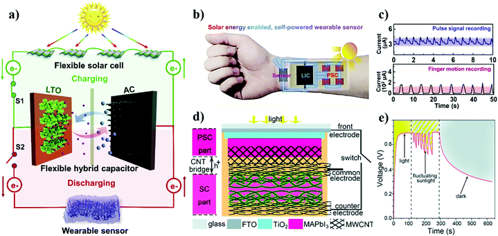 |
| | Fig. 9 Schematic of the perovskite photovoltaic cell powered supercapacitor and photocapacitor and their respective responses: (a) scheme of the flexible PSC–LIC–sensor system. (b) Scheme of wearable PSC–LIC–sensor integrated system. (c) The output current response of pulse signal (upper panel) and finger motion (lower panel) under light illumination. Reprinted from Li et al., flexible perovskite solar cell-driven photo-rechargeable lithium-ion capacitor for self-powered wearable strain sensors, Nano Energy, 60, 247–56.127 Copyright 2019, with permission from Elsevier. (d) Scheme of the photocapacitor made by organometal halide perovskite and PANI/CNT composites integrated using a CNT bridge. (e) The performance of a photocapacitor under different illumination conditions. Reproduced from ref. 129 with permission from The Royal Society of Chemistry. | |
3. Internet of things (IoT) sensors
Combining photovoltaic cells with the low-power radio frequency (RF) backscatter-based IoT sensors is a new approach to ubiquitous sensing for indoor applications.130–134 The perovskite based photovoltaics can provide the necessary low power for these sensors enabling their operation for a long time. Kantareddy et al. reported a self-powered perovskite wireless temperature sensor with a 4 meter communication range.131 Under 1 sun illumination, the PSC with the configuration of FTO/TiO2/(Rb0.01Cs0.05(FA0.83MA0.17)0.94Pb(I0.83Br0.17)3)/Spiro-OMeTAD/Au exhibited a Voc of 4.3 V, a Jsc of 3.7 mA cm−2, an FF of 0.6, and a PCE of 10.1% with an active area of 1.06 cm2. This device was able to generate enough power to boot up a radio frequency identification (RFID) device that required 10–45 μW energy. Similarly, Mathews et al. demonstrated an approach to integrate a wireless temperature sensor with PSCs acting as an external power source.132 An integrated array of three photovoltaic cells, with the configuration of FTO/TiO2/(Rb0.01Cs0.05)(MAxFA1−x)0.94Pb(BrxI1−x)3/Spiro-OMeTAD/Au achieved a Voc, Jsc, and PCE of 2.62 V, 46 μA cm−2 and 13.2%, respectively. The output was 14.5 μW under a light intensity of 0.16 mW cm−2 which is enough to power an RFID temperature sensor. The whole wireless temperature device was operational for over 8 h with regular measurements at 1.24 s intervals upon illumination by ambient light.
4. Transistors and photocatalysis
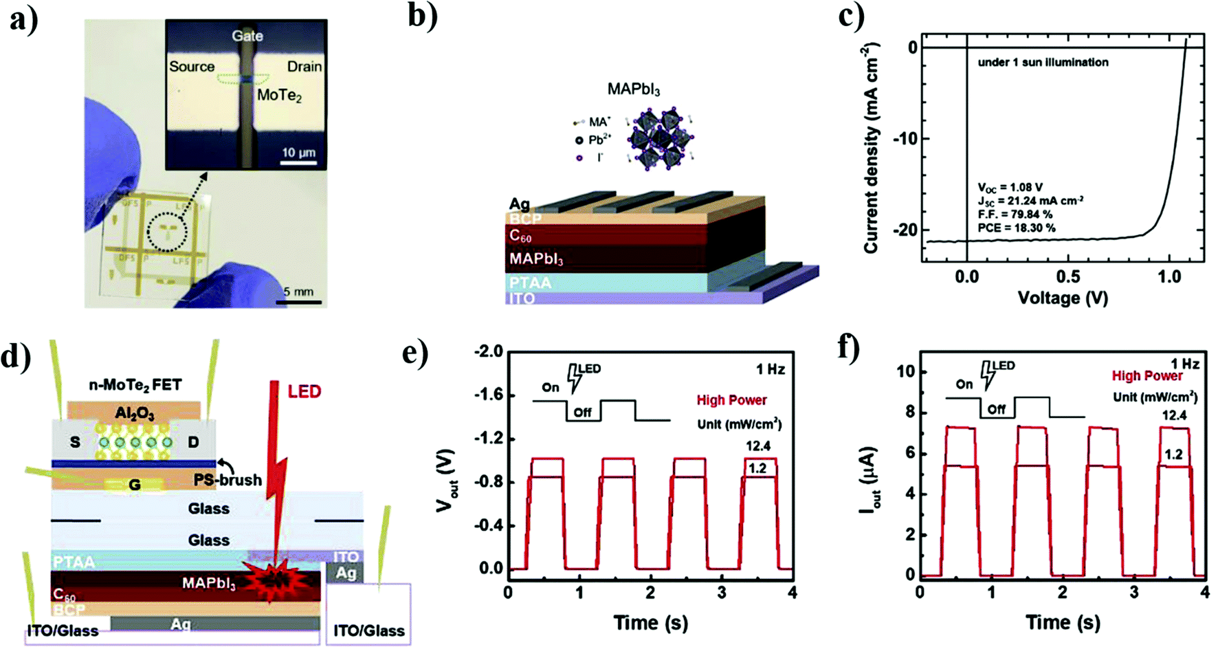
Photovoltaic devices have also been coupled with transistors74,135–139 and electrochemical cells for degradation of organic pollutants,140,141 due to their high Voc (0.9 V to 1.5 V) and power generation capacity. Jeong et al. reported a MAPbI3 film coupled with PTAA, exhibiting a Jsc and Voc of ∼21 mA cm−2 and ∼1.08 V, respectively, with 18.3% PCE.135 The Voc under red-LED could effectively gate the MoTe2 field-effect transistors (FET) modulating the drain current (ID), which could turn on/off an OLED pixel (Fig. 10). Chen et al. reported that multi-walled CNTs and a methylamine (CH3NH2) modified perovskite achieved a PCE of 10.39%.140 It was demonstrated that the CNT-incorporated MAPbI3 perovskite thin film formed a smooth heterojunction structure, which facilitated the separation and transfer of charges. Also, CH3NH2 could self-heal the perovskite surface while maintaining high crystallinity. This inhibited the charge recombination and improved the efficiency of the device. Thus, the CNT/CH3NH2 perovskite exhibited a high Jsc value of 22.02 mA cm−2. Combined with the CNT/TiO2 photoanodes and the perovskite PSC (as power source), the system exhibited an efficient degradation of rhodamine B to almost 100% within 80 min.
 |
| | Fig. 10 Perovskite solar cell powered FET and the corresponding photosensitive response: (a) photo image and optical microscope image (inset) of n-MoTe2 FET. (b) Scheme of the MAPbI3-based perovskite PV cells. (c) Current density–voltage curve of the PV cell measured under 1 sun illumination. (d) Cross-section scheme of the packaged device. Light intensity-dependent (e) Vout and (f) Iout of the packaged device under periodic red LED illumination, respectively. Reprinted from Jeong et al., Integrated advantages from perovskite photovoltaic cell and 2D MoTe2 transistor towards self-power energy harvesting and photosensing, Nano Energy, 63, 103833.135 Copyright 2019, with permission from Elsevier. | |
5. Photovoltachromic cells
Photovoltachromic cells (PVCCs) can adjust the optical transmittance and coloration by their photovoltaic behaviors.142–144 They are of interest for applications in smart windows in buildings and vehicles to manage daylight admittance. A photovoltachromic device integrated with a perovskite based photovoltaic cell enables their operation without an external bias.145–147 Park et al. used a ligand assisted re-precipitation method (LARP) to synthesize CH3NH3PbX3 (X = Cl, Br, I, and their mixtures) metal halide perovskite nanocrystals (MHP NCs).148 The LARP method used N,N-dimethylformamide (DMF) as a good solvent and toluene as a poor solvent. While the good solvent possessed a slower evaporation rate, the poor solvent (toluene) induced crystallization leading to the precipitation of MHP NCs. The authors tuned the energy bandgap and corresponding absorption and emission characteristics of the MAPbX3 MHP NCs by carefully adjusting the ratio of DMF and toluene. The typical size of the MAPbBr3 MHP NCs was ∼5 nm. Owing to their reduced size, the MHP NCs exhibited strong luminescence and high quantum yield. The blue, green, and red MHP NCs were utilized to fabricate a panchromatic photodetector cell that showed a full-colored emission spectrum spanning 435–631 nm (Fig. 11a and b). The effective panchromatic photon harvesting was attributed to the individual absorption of blue, green, and red light by the corresponding MHP NCs and the independent transfer of the photogenerated electrons into the mesoporous TiO2 electrode. Cannavale et al. were amongst the first to report a self-powered photovoltachromic device integrated using a perovskite and an electrochromic supercapacitor (ECS).149 Here, the ECS included a layer of WO3 which could store charges and change the color at the same time owing to the change of the chemical state in W. As reported, WO3 is transparent, and WO3− is colored.146 As seen in Fig. 11c–e, once the device was exposed to solar illumination, the perovskite was capable of generating enough power to activate the coloring of WO3 without requiring any external bias. Therefore, the device processed a chromic transition from semi-transparent to dark blue when irradiated by solar light. The perovskite layer presented a Voc of 0.68 V, a Jsc of 12.5 mA cm−2, an FF of 0.63, and a PCE of 5.5%. As for the PVCC, it showed average visible transmittance (AVT) of 15.9%. Illuminated at AM 1.5 sunlight, the cell's AVT changed to 5.5%. Similarly, Zhou et al. vertically stacked PSC with MoO3/Au/MoO3 (MAM), all transparent electrode and WO3 ECS to produce a photovoltachromic supercapacitor (PVCSs) which can store the electrochemical energy accompanied by color change.150 This design not only provided a seamless integration of energy harvesting and storage device but also improved photostability. The photocharging process changed the color of the PVCSs from transparent to dark blue. During the fully charged state, the colored PVCSs blocked off most of the light automatically turning the PSC into the low power operating state and preventing the cell from long-time exposure, thereby prolonging the device lifetime. The transparent electrodes facilitated the possibility of PSC to be illuminated from both sides. In the co-cathode structure, the FTO glass served as the co-cathode for both PSC and ECS. While for the co-anode structure, the MAM electrode served as a co-anode for both PSC and ECS. When PSC was in the co-anode mode (or the co-cathode), PVCS with the light illumination demonstrated a Voc of 0.983 V (or 1.000 V), a Jsc of 12.46 mA cm−2 (or 18.17 mA cm−2), an FF of 0.654% (or 0.654%), and a PCE of 8.25% (or 11.89%). With the color change, the PCEs of the co-anode and co-cathode PVCSs decreased to 3.73% and 2.26%, respectively.
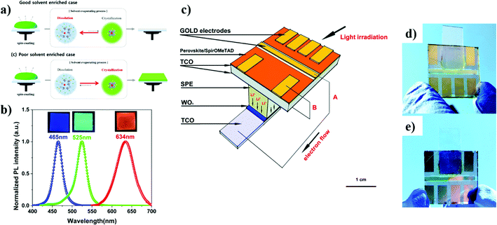 |
| | Fig. 11 Perovskite based panchromatic photodetectors and photovoltachromic devices: (a) scheme of the good–poor solvent enriched preparation process of MMH NC films by spin-coating. (b) Normalized PL spectra of blue, green, and red MHP NC-films. Reprinted from Park et al., Synthesis of post-processable metal halide perovskite nanocrystals via the modified ligand-assisted re-precipitation method and their applications in self-powered panchromatic photodetectors, J. Ind. Eng. Chem., 92, 167–173.148 Copyright 2020, with permission from Elsevier. (c) Scheme of axonometric view of the photovoltachromic device. The optical image of the device under (d) bleached and (e) colored conditions. Reproduced from ref. 149 with permission from The Royal Society of Chemistry. | |
6. Pressure sensors
Flexible pressure sensors have numerous applications in areas such as artificial electronic skins,145,151,152 health monitoring devices,153–156 soft robotics,157–159 and wearable technology.160–165 It also improves the seamless interfacing of such devices with the environment to act as a medium for information collection to drive robotics and human–artificial intelligence interactions.166 The OLHP based self-powered pressure sensors and the corresponding device characteristics are listed in Table 4.
Table 4 Summary of OLHP based pressure-sensitive devices and their associated parameters
| Device type |
Device architecture |
Peak output voltage/Voc |
Peak output current/Jsc |
Sensitivity/minimum pressure |
Application and features |
Ref. |
| Mechanoluminescent |
ZnS:Cu-PDMS/PET/ITO/SnO2/CH3NH3Pb(Br0.1I0.9)3/Spiro-OMeTAD/Au |
|
|
0.095 kPa−1 |
Self-powered luminescent device, sensitivity range: 11 kPa to 460 kPa |
162
|
| Piezoelectric effect assisted sensor |
PI-Ti/Au/PDMS/MAPbI3–PVDF/ITO-PET |
45.6 V |
4.7 μA cm−2 |
|
PEG could power commercial LEDs under an applied force of 50 N, a high dielectric constant of ∼56 at 1 kHz, and remanent polarization of 0.83 μC cm−2 |
167
|
| Ni/PVDF–MAPbI3 nanofiber mat/Cu |
∼220 mV |
18.2 pA |
|
Self-powered pyroelectric temperature sensor, pyroelectric coefficient of ∼44 pC m−2 K−1 with a response and reset times of ∼1.14 and ∼1.25 s, respectively |
158
|
| Ag/MAPbBr3–PVDF/Ag |
∼0.25 V |
|
0.02 V mm−1 |
Self-powered vibration sensor |
168
|
| Polyester/Cu/FAPbBr2I–PVDF/Cu/polyester |
85 V |
∼30 μA |
|
Self-powered integrated wireless electronic node, peak output power density of 10 μW cm−2 |
159
|
| Glass/3 at% Al doped ZnO (AZO)/Au/AZO/MAPbI3/SiO2/AZO/Au/AZO |
125.6 ± 2.4 mV and −30.2 ± 8.2 mV |
0.8 nA |
8.34 mV kPa−1 and 0.02 nA kPa−1 |
Self-powered light and pressure sensor, sensitivity range: 5 to 40 kPa |
169
|
|
|
|
|
|
|
Response speed: 0.066/0.320 s |
| ZnO nanosheets on Au/MAPbI3/Au |
|
|
0.57 kPa−1 |
Self-powered tactile sensor, sensitivity range: 0.5 kPa to 76 kPa; |
166
|
| ITO/ZnO nanosheets on Au/PS–MAPbI3/Au |
∼325 mV |
∼0.12 mA cm−2 |
19.77 kPa−1 |
Self-powered tactile sensor, sensitivity range: 4 Pa to 450 kPa |
170
|
6.1 Mechanoluminescent device
Shohag et al. reported a flexible pressure sensor by integrating a mechanoluminescent device with a ∼500 nm thick organometal halide perovskite.162 In this work, the authors attempted at reducing the defect density of the perovskite by incorporating bromine which led to reduced trapping of charge carriers at the grain boundaries and hence, enhanced the efficiency. An applied mechanical force led the ZnS:Cu crystals to emit mechanoluminescence at ∼543 nm, which could be then absorbed by the ultrathin layer of perovskite (MAPb(Br0.1I0.9)3) to generate a photocurrent. The photocurrent generated in the perovskite layer increased with the increase in the intensity of light emitted from the ZnS:Cu layer, in direct proportion to the applied pressure. The sensor was able to detect pressure from 11 kPa to 460 kPa with a sensitivity of 0.095 kPa−1. The sensor also exhibited a steady response over 1000 bending cycles, which is promising for monitoring health signals.
6.2 Piezoelectric effect assisted sensing
MAPbI3 is a semi-conductor and poly(vinylidene fluoride) (PVDF) is a piezoelectric material. Researchers have combined these two materials to develop self-powered pressure sensors based on their combined properties. For example, Jella et al. constructed a flexible and wearable piezoelectric generator (PEG) by using the MAPbI3 perovskite and PVDF as a piezoelectric flexible polymer matrix.167 The strong dipolar interactions between MA+ and the fluorine groups of the PVDF (–CF2–) result in a high dielectric constant, low leakage current, and high stability. As observed in Fig. 12, under an applied force, macro-dipoles are formed resulting in charge accumulation at the MAPbI3–PVDF interface with opposite polarity, so the charge density of the electrode decreases generating a positive signal while the releasing process produced a negative signal. The device showed a Voc of 45.6 V and a Jsc of 4.6 μA cm−2 with high mechanical stability. The generated output can power commercial LEDs under a 50 N applied force by finger tapping. Sultana et al. produced a flexible self-powered perovskite based piezoelectric nanogenerator (P-PNG) by electrospinning PVDF nanofibers and MAPbI3.158 The mechanical vibration led to a change of output power density with a piezoelectric coefficient of ∼19.7 pC N−1 which shows appreciable potential for a pressure sensor. The Voc increased with the frequency of applied stress as more charges are generated. As illustrated in Fig. 13a–d, at 4 Hz, the Voc reached a maximum of 220 mV while gradually decreasing to 100 mV at 15 Hz. The authors also measured the stability of the device, which showed a stable response for 60000 cycles at 4 Hz with a 7.5 N applied force. Sultana et al. also developed a cantilever structured self-powered vibration sensor (SPVS) for low-frequency vibration detection by combining MAPbBr3 and PVDF.168 Based on the intrinsic properties of the PEG, the larger displacement of the tip increased the strain applied on the film resulting in an output voltage. Thus, the output voltage of the SPVS was able to sense the frequency and amplitude of vibration with a sensitivity of 0.02 V mm−1. This device showed the possibility of detecting the vibrations from railway or construction equipment without an external bias. Recently, Khan et al. presented a flexible and highly porous FAPbBr2I–PVDF P-PNG assembly.159 The high strain of the self-assembled highly ordered polymer scaffold and enhanced relative permittivity of the perovskite led to a 5 fold improvement in the strain-induced piezo potential (∼85 V) and 15 times higher current (∼30 μA) in the perovskite-polymer composite P-PNG relative to those of the pristine PVDF PNG, at an applied load of 138 g. Utilizing the P-PNG, the authors further demonstrated a self-powered universal wireless electronics node (SIWEN) capable of communicating remotely with personal electronics. Energy harvesting from a real-life scenario such as automobile vibrations and biomechanical motion was also demonstrated. Eom et al. used the CVD method to fabricate a 500 nm thin film of MAPbI3.169 The film was stable for a month under ambient conditions. Owning to an intrinsic piezoelectric property of MAPbI3, the device showed sensitivity to both pressure and light. The MAPbI3 film had a linear sensitivity to a pressure of 8.34 mV kPa−1 and 0.02 nA kPa−1 within a pressure range of 40 kPa, generated by finger touch. There was a time delay of 0.072 and 0.087 s in detection on applying and removing the pressure. The delay was attributed to the domain switching due to applied pressure on the film. In an interesting work, Saraf et al. combined a layer of ZnO nanosheets as a pressure-sensitive electron extraction layer on the MAPbI3 film (Fig. 13e and f).166 A small external bias was applied for few minutes to the MAPbI3 film to induce polarization effects capable of generating spontaneous voltage and current response upon light illumination once the external bias was removed. The pressure applied on the top ZnO layer increased the interfacing area between the MAPbI3 film and the ZnO layer, leading to a higher collection of electrons. This action increased the value of Jsc (or Voc) in proportion to the applied pressure, as shown in Fig. 13f. The sensor exhibited a linear response from 0.5 kPa to 76 kPa with a sensitivity of 0.57 kPa−1. After 100 load cycles, the device had a stable current generation density of 0.2 mA cm−2. This tactile sensor demonstrated a low energy cost as it could operate over 72 h after poling for 5 min at 1.5 V μm−1. To further improve the stability of the sensor, Saraf et al. used hydrophobic PS with MAPbI3. The resultant polymer–perovskite hybrid device displayed stability under ambient conditions for over 1000 h.170 Also, the inclusion of the polymer led to a softer film with a lower modulus which dissipated the force stimuli leading to a wide operating range. Once poled, the film was functional as a self-driven light-powered tactile sensor for 120 h and could be re-poled for continued operational performance. The light-powered tactile sensor fabricated by the assembly of 1 wt% PS–MAPbI3 film and ZnO exhibited a wide operating range from 4 Pa up to 333 kPa with linear response and a sensitivity of 19.77 kPa−1.
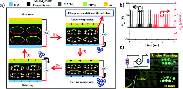 |
| | Fig. 12 Schematic of piezoelectric based origin of self-powered operation in perovskite–polymer composite and the generated response: (a) scheme of the MAPbI3–PVDF composite-based PEG working mechanism. (b) The Voc and Jsc response of MAPbI3–PVDF PEG under an applied force of 50 N. (c) Photo images of an instant turn on 10 green LEDs by rectified electric power from the harvesting device. Insets present the scheme of the circuit and lighting of LEDs in dark. Reprinted from Jella et al., Enhanced output performance of a flexible piezoelectric energy harvester based on stable MAPbI3–PVDF composite films, Nano Energy, 53, 46–56.167 Copyright 2018, with permission from Elsevier. | |
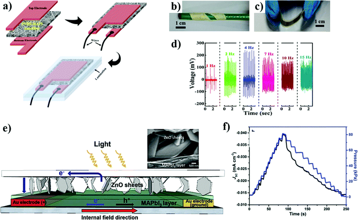 |
| | Fig. 13 Device schematic, images, and the electro-optical response of P-PNG and perovskite based self-powered tactile sensor: (a) PVDF–MAPI nanofiber mat sandwiched between two electrodes. (b) Optical image of the flexible P-PNG wrapped on a pen. (c) Optical image of bent P-PNG. (d) Output voltage response of P-PNG of applied force under different frequencies. Reprinted with permission from Sultana et al., ACS Appl. Mater. Interfaces, 11, 27279–27287.158 Copyright © 2019 American Chemical Society. (e) Schematic of the solar-powered tactile sensor. Inset shows SEM image of ZnO sheets on the perovskite layer. (f) The response of Jsc under the stepped applied pressure under 1 sun illumination. Reproduced with permission from Saraf et al., Adv. Mater., 30, 1705778.166 © 2018 WILEY-VCH Verlag GmbH & Co. KGaA, Weinheim. | |
7. Gas sensors
Today, there is an increasing need for portable self-powered gas sensing devices to monitor personal health, toxic gas release, and safety in public space.141,154,171–176 Chen et al. synthesized a self-powered nitrogen dioxide (NO2) sensing device based on FA0.80MA0.15Cs0.05PbI2.55Br0.45 (FMCPIB) perovskites.141 The authors fabricated a photovoltaic cell with the vertical configuration of FTO/TiO2/FMCPIB/carbon. The authors believed that NO2 can undergo interaction with the amine cation of FMCPIB. This interaction was attributed to reducing the defects in the perovskite film which decreases the charge recombination and hence increasing the density of free charge carriers. Fig. 14 represents the device performance of NO2 detection at room temperature under O2 rich conditions. A linear relationship up to 8 ppm with a 0.2 ppm detection limit under ambient conditions was observed. A higher NO2 concentration led to a higher output current due to the interaction between NO2 and FMCPIB. Owing to the functionality of the FMCPIB to act as a gas sensor, light harvester, and capacitive energy storage material (due to mobile ions), the self-powered device stayed in operation for 1.7 h in dark without requiring an external power supply. The measured response and recovery times were 17 s and 126 s, respectively. Such gas sensing ability banking on the inherent material properties of OLHP may pave new ways to monitor environmental safety using self-powered sensors.
 |
| | Fig. 14 Design and self-powered chemical response of the FMCPIB-based gas sensor at room temperature: (a) scheme of the FMCPIB-based gas sensor. (b) The current response of the FMCPIB devices with the injection of 8 ppm NO2. (c) The sensor response for six different gases. (d) The sensor response as a function of the NO2 concentration in the self-powered mode. Reproduced with permission from Chen et al., Adv. Opt. Mater., 8, 1901863.141 © 2020 WILEY-VCH Verlag GmbH & Co. KGaA, Weinheim. | |
Challenges and future prospects
Continuous research has led to significant advances in the OLHP based self-powered devices both in terms of their performance and expanding their applications. Various devices besides solar cells, such as PDs, supercapacitors, and TENGs, are being fabricated primarily using OLHP as a photosensitive layer. The development of self-powered electroluminescent devices using OLHP can also benefit from an increased research focus. The challenge lies in the typical high voltage requirement for generating appreciable luminescence. The use of polarization effects in OLHP is a potential route for such devices, with the research required to understand and enhance these characteristics for the generation of greater energy and electric potential. The inherent stability issue of the perovskite material is a major challenge that persists due to the inherent structure of the material (high ion mobilities) and its sensitivity to multiple external factors (such as humidity, oxygen, illumination, and temperature). Strategies such as interfacial engineering, additive integration, doping, and encapsulation are being widely adopted to reduce perovskite degradation. A significant scope also exists for the improvement of the inherent perovskite structure and composition. These combined efforts result in improving the lifetime of the OLHP based devices and should continue to progress them towards commercial viability. With the concerns of toxicity surrounding lead, there are ongoing efforts of substituting it with other divalent ions such as Sn, Ge, Bi, and Sb, but the resulting reduction in performance needs to be addressed in order to develop lead-free perovskites.177,178
At a macroscale, as it stands, the majority of OLHP based self-powered devices and sensors are rigid. Although, in the last few years flexible transducers are being researched and reported with greater intensity, they experience performance degradation during long-term operations. Most wearable and portable electronic devices and sensors mandate the ability to be stretched and bent over a couple of thousand cycles without incurring significant decay in output over time. Alternatives for 3D OLHP such as 2D, 1D, and 0D OLHP may offer enhanced flexibility and might provide viable options.179–182 Equally critical is the need for developing appropriate substrates and electrodes for long-term device operation while ensuring wearability comfort. Furthermore, it is worth considering that almost all OLHP self-powered portable and wearable devices are tested at 1 sun. However, the indoor performance of these devices with limited illumination is rarely reported. Therefore, developing standard protocols for testing devices under such limited light conditions need to be developed as this will allow a more accurate comparison of devices.
Although low levels of the output signals and non-continuous operation seem to impede the overall capability of the OLHP based self-driven devices and sensors, several other major factors contribute to hinder the commercial viability of such perovskite-based transducers. Currently, there is a lack of a standardized large-scale manufacturing process that could ensure performance consistency amongst batches of the same device. Besides, there is limited research available over performance–cost analysis specific to the OLHP self-powered devices that could drive them from a lab prototype to a commercial finished product. OLHP is considered a low-cost material compared to other semiconductors (such as Si and organic compounds); however, a more detailed cost analysis is required for the quantification of its cost advantage (including Pb recycling needs). Techniques such as printing need to be promoted to drive up large scale cost-effective production of the OLHP based self-powered devices. The use of advanced microfabrication and nanofabrication techniques can further expand the integration of other flexible electronic, photonic, and optoelectronic devices with OLHP as an energy harvester.
In summary, significant advancements have been made in OLHP based self-powered applications, but still there are critical challenges that need to be addressed before they can be considered commercially viable products. The rapid development of materials science, processing, and manufacturing technology can enable the progress of the OLHP based self-powered system in our day-to-day life at a rapid pace and the commercialization of OLHP based photovoltaic cells provides important lessons for this road map.
Author contributions
Avi Mathur: conceptualization, investigation, and writing – original draft. Hua Fan: investigation and writing – original draft. Vivek Maheshwari: conceptualization, funding acquisition, resources, writing – review & editing, and supervision.
Conflicts of interest
There are no conflicts to declare.
Acknowledgements
This work was supported by the University of Waterloo, Gerald Schwartz and Heather Reisman Foundation, Canada Foundation for Innovation, Early Researcher Award from the Ministry of Research and Innovation and Science, Ontario, and NSERC Canada.
References
- L. Atzori, A. Iera and G. Morabito, Comput. Networks, 2010, 54, 2787–2805 CrossRef.
- F. Xia, L. T. Yang, L. Wang and A. Vinel, Int. J. Commun. Syst., 2012, 25, 1101 CrossRef.
- Y. Yuehong, Y. Zeng, X. Chen and Y. Fan, J. Ind. Inf. Integr., 2016, 1, 3–13 Search PubMed.
- C. Xu, Y. Song, M. Han and H. Zhang, Microsyst. Nanoeng., 2021, 7, 1–14 CrossRef.
- M. J. Cima, Nat. Biotechnol., 2014, 32, 642–643 CrossRef CAS PubMed.
-
N. Xu, S. Rangwala, K. K. Chintalapudi, D. Ganesan, A. Broad, R. Govindan and D. Estrin, A wireless sensor network for structural monitoring, 2004 Search PubMed.
- J. Kim, R. A. Swartz, J. P. Lynch, J.-J. Lee and C.-G. Lee, Smart Struct. Syst., 2010, 6, 505–524 CrossRef.
-
F. Zhang, X. Liu, S. A. Hackworth, R. J. Sclabassi and M. Sun, In vitro and in vivo studies on wireless powering of medical sensors and implantable devices, IEEE, 2009.
-
D. Fitzpatrick, Implantable electronic medical devices, Elsevier, 2014 Search PubMed.
- F. Larsson, P. Andersson, P. Blomqvist and B.-E. Mellander, Sci. Rep., 2017, 7, 1–13 CrossRef CAS PubMed.
- J. Sun, J. Li, T. Zhou, K. Yang, S. Wei, N. Tang, N. Dang, H. Li, X. Qiu and L. Chen, Nano Energy, 2016, 27, 313–319 CrossRef CAS.
- R. W. Keyes, IBM J. Res. Dev., 1988, 32, 84–88 Search PubMed.
- P. Glynne-Jones and N. White, Sens. Rev., 2001, 21, 91–98 CrossRef.
- Q. Zheng, Q. Tang, Z. L. Wang and Z. Li, Nat. Rev. Cardiol., 2020, 1–15 Search PubMed.
-
K. M. Reilly, M. T. Birner and N. G. Johnson, Measuring air quality using wireless self-powered devices, IEEE, 2015.
- Z. Liu, B. Cho, T. Ouyang and B. Feldman, Anal. Chem., 2012, 84, 3403–3409 CrossRef CAS PubMed.
- F.-R. Fan, L. Lin, G. Zhu, W. Wu, R. Zhang and Z. L. Wang, Nano Lett., 2012, 12, 3109–3114 CrossRef CAS PubMed.
- J. Zhao, R. Ghannam, K. O. Htet, Y. Liu, M. K. Law, V. A. Roy, B. Michel, M. A. Imran and H. Heidari, Adv. Healthcare Mater., 2020, 9, 2000779 CrossRef CAS PubMed.
-
J. Twidell and T. Weir, Renewable energy resources, Routledge, 2015 Search PubMed.
- A. Kojima, K. Teshima, Y. Shirai and T. Miyasaka, J. Am. Chem. Soc., 2009, 131, 6050–6051 CrossRef CAS PubMed.
- National Renewable Energy Laboratory – Best research-cell efficiencies chart, https://www.nrel.gov/pv/cell-efficiency.html, accessed April, 2021.
- K. P. Ong, T. W. Goh, Q. Xu and A. Huan, J. Phys. Chem. A, 2015, 119, 11033–11038 CrossRef CAS PubMed.
- C. Quarti, E. Mosconi, J. M. Ball, V. D'Innocenzo, C. Tao, S. Pathak, H. J. Snaith, A. Petrozza and F. De Angelis, Energy Environ. Sci., 2016, 9, 155–163 RSC.
- Q. Chen, N. De Marco, Y. M. Yang, T.-B. Song, C.-C. Chen, H. Zhao, Z. Hong, H. Zhou and Y. Yang, Nano Today, 2015, 10, 355–396 CrossRef CAS.
- F. Hao, C. C. Stoumpos, D. H. Cao, R. P. Chang and M. G. Kanatzidis, Nat. Photonics, 2014, 8, 489 CrossRef CAS.
- L. Chouhan, S. Ghimire, C. Subrahmanyam, T. Miyasaka and V. Biju, Chem. Soc. Rev., 2020, 49, 2869–2885 RSC.
- S. Pang, H. Hu, J. Zhang, S. Lv, Y. Yu, F. Wei, T. Qin, H. Xu, Z. Liu and G. Cui, Chem. Mater., 2014, 26, 1485–1491 CrossRef CAS.
- J. Song, J. Li, X. Li, L. Xu, Y. Dong and H. Zeng, Adv. Mater., 2015, 27, 7162–7167 CrossRef CAS PubMed.
- Q. Shan, J. Song, Y. Zou, J. Li, L. Xu, J. Xue, Y. Dong, B. Han, J. Chen and H. Zeng, Small, 2017, 13, 1701770 CrossRef PubMed.
- L. Xu, J. Li, B. Cai, J. Song, F. Zhang, T. Fang and H. Zeng, Nat. Commun., 2020, 11, 1–12 Search PubMed.
- J. Chen, J. Wang, X. Xu, J. Li, J. Song, S. Lan, S. Liu, B. Cai, B. Han and J. T. Precht, Nat. Photonics, 2021, 15, 238–244 CrossRef CAS.
- J. Sun, J. Wu, X. Tong, F. Lin, Y. Wang and Z. M. Wang, Adv. Sci., 2018, 5, 1700780 CrossRef PubMed.
-
R. Saraf and V. Maheshwari, Functional Tactile Sensors, Elsevier, 2021, pp. 141–158 Search PubMed.
- X. Zhang, X. Dong, S. Wang, H. Liu, W. Hu and X. Li, Chem. Eng. J., 2021, 404, 125957 CrossRef CAS.
- F. P. G. de Arquer, A. Armin, P. Meredith and E. H. Sargent, Nat. Rev. Mater., 2017, 2, 1–17 Search PubMed.
- Y. Xie, B. Zhang, S. Wang, D. Wang, A. Wang, Z. Wang, H. Yu, H. Zhang, Y. Chen and M. Zhao, Adv. Mater., 2017, 29, 1605972 CrossRef PubMed.
- E. Dupont, M. Byloos, M. Gao, M. Buchanan, C.-Y. Song, Z. Wasilewski and H. Liu, IEEE Photonics Technol. Lett., 2002, 14, 182–184 Search PubMed.
- C. Chen, K. Choi, W. Chang and D. Tsui, Appl. Phys. Lett., 1998, 72, 7–9 CrossRef CAS.
-
S. Donati, Photodetectors: devices, circuits and applications, John Wiley & Sons, 2021 Search PubMed.
- G. Konstantatos, Nat. Commun., 2018, 9, 5266 CrossRef CAS PubMed.
- X. Feng, M. Tan, M. Li, H. Wei and B. Yang, Nano Lett., 2021, 21, 1500–1507 CrossRef CAS PubMed.
- Y. Liu, Y. Zhang, X. Zhu, Z. Yang, W. Ke, J. Feng, X. Ren, K. Zhao, M. Liu and M. G. Kanatzidis, Sci. Adv., 2021, 7, eabc8844 CrossRef CAS PubMed.
- T. M. H. Nguyen, S. Kim and C. W. Bark, J. Mater. Chem. A, 2021, 9, 1269–1276 RSC.
- C. Perumal Veeramalai, S. Feng, X. Zhang, S. V. N. Pammi, V. Pecunia and C. Li, Photonics Res., 2021, 9, 968–991 CrossRef.
- L. Dou, Y. M. Yang, J. You, Z. Hong, W.-H. Chang, G. Li and Y. Yang, Nat. Commun., 2014, 5, 1–6 Search PubMed.
- M. Zhang, M. Ye, W. Wang, C. Ma, S. Wang, Q. Liu, T. Lian, J. Huang and Z. Lin, Adv. Mater., 2020, 32, 2000999 CrossRef CAS PubMed.
- B. Wang, M. Zhang, X. Cui, Z. Wang, M. Rager, Y. Yang, Z. Zou, Z. L. Wang and Z. Lin, Angew. Chem., 2020, 132, 1628–1635 CrossRef.
- M. Zhang, X. Cui, Y. Wang, B. Wang, M. Ye, W. Wang, C. Ma and Z. Lin, Nano Energy, 2020, 71, 104620 CrossRef CAS.
- Z. Wang, R. Yu, C. Pan, Z. Li, J. Yang, F. Yi and Z. L. Wang, Nat. Commun., 2015, 6, 1–7 Search PubMed.
- J. Yu, X. Chen, Y. Wang, H. Zhou, M. Xue, Y. Xu, Z. Li, C. Ye, J. Zhang and P. A. Van Aken, J. Mater. Chem. C, 2016, 4, 7302–7308 RSC.
- Y. Zhu, Z. Song, H. Zhou, D. Wu, R. Lu, R. Wang and H. Wang, Appl. Surf. Sci., 2018, 448, 23–29 CrossRef CAS.
- H. Zhou, L. Yang, P. Gui, C. R. Grice, Z. Song, H. Wang and G. Fang, Sol. Energy Mater. Sol. Cells, 2019, 193, 246–252 CrossRef CAS.
- X. Yang, Y. Zhu, H. Zhou, Z. Song, R. Liu, L. Shen and H. Wang, Appl. Surf. Sci., 2020, 504, 144468 CrossRef CAS.
- Z. Liu, X. Liu, B. Sun, X. Tan, H. Ye, J. Zhou, Z. Tang, T. Shi and G. Liao, Adv. Mater. Technol., 2020, 5, 2000260 CrossRef CAS.
- H. Zhou, J. Mei, M. Xue, Z. Song and H. Wang, J. Phys. Chem. C, 2017, 121, 21541–21545 CrossRef CAS.
- J. Ghosh, G. Natu and P. Giri, Org. Electron., 2019, 71, 175–184 CrossRef CAS.
- D. H. Shin, S. H. Shin, S. G. Lee, S. Kim and S.-H. Choi, ACS Sustainable Chem. Eng., 2019, 7, 19961–19968 CrossRef CAS.
- Y. Cheng, Z. Shi, S. Yin, Y. Li, S. Li, W. Liang, D. Wu, Y. Tian and X. Li, Sol. Energy Mater. Sol. Cells, 2020, 204, 110230 CrossRef CAS.
- L. Shen, Y. Fang, D. Wang, Y. Bai, Y. Deng, M. Wang, Y. Lu and J. Huang, Adv. Mater., 2016, 28, 10794–10800 CrossRef CAS PubMed.
- Q. Shan, C. Wei, Y. Jiang, J. Song, Y. Zou, L. Xu, T. Fang, T. Wang, Y. Dong and J. Liu, Light: Sci. Appl., 2020, 9, 1–9 CrossRef PubMed.
- C. Lan, H. Zou, L. Wang, M. Zhang, S. Pan, Y. Ma, Y. Qiu, Z. L. Wang and Z. Lin, Adv. Mater., 2020, 32, 2005481 CrossRef CAS PubMed.
- Z. Li, H. Li, K. Jiang, D. Ding, J. Li, C. Ma, S. Jiang, Y. Wang, T. D. Anthopoulos and Y. Shi, ACS Appl. Mater. Interfaces, 2019, 11, 40204–40213 CrossRef CAS PubMed.
- T. Pang, R. Jia, Y. Wang, K. Sun, Z. Hu, Y. Zhu, S. Luan and Y. Zhang, J. Mater. Chem. C, 2019, 7, 609–616 RSC.
- L. Ren, M. Wang, M. Li, S. Wang, S. Wang, Y. Zhao, M. A. Iqbal and K. Jin, Opt. Mater., 2020, 100, 109687 CrossRef CAS.
- K. Pandey, M. Chauhan, V. Bhatt, B. Tripathi, P. Yadav and M. Kumar, RSC Adv., 2016, 6, 105076–105080 RSC.
- J. Li, S. Yuan, G. Tang, G. Li, D. Liu, J. Li, X. Hu, Y. Liu, J. Li and Z. Yang, ACS Appl. Mater. Interfaces, 2017, 9, 42779–42787 CrossRef CAS PubMed.
- Q. Zeng and Z. Liu, Adv. Electron. Mater., 2018, 4, 1700335 CrossRef.
- M. Pandey, R. Soni, A. Mathur, A. Singh, A. K. Singh, S. Raghavan and U. Chandni, Phys. Rev. Appl., 2019, 12, 064032 CrossRef CAS.
- D. Sarkar, W. Liu, X. Xie, A. C. Anselmo, S. Mitragotri and K. Banerjee, ACS Nano, 2014, 8, 3992–4003 CrossRef CAS PubMed.
- N. Rohaizad, C. C. Mayorga-Martinez, Z. K. Sofer and M. Pumera, ACS Appl. Mater. Interfaces, 2017, 9, 40697–40706 CrossRef CAS PubMed.
- S. Barua, H. S. Dutta, S. Gogoi, R. Devi and R. Khan, ACS Appl. Nano Mater., 2017, 1, 2–25 CrossRef.
- J. H. Lee, J. Y. Park, E. B. Cho, T. Y. Kim, S. A. Han, T. H. Kim, Y. Liu, S. K. Kim, C. J. Roh and H. J. Yoon, Adv. Mater., 2017, 29, 1606667 CrossRef PubMed.
- A. Di Bartolomeo, A. Grillo, F. Urban, L. Iemmo, F. Giubileo, G. Luongo, G. Amato, L. Croin, L. Sun and S. J. Liang, Adv. Funct. Mater., 2018, 28, 1800657 CrossRef.
- F. Bai, J. Qi, F. Li, Y. Fang, W. Han, H. Wu and Y. Zhang, Adv. Mater. Interfaces, 2018, 5, 1701275 CrossRef.
- L. H. Zeng, Q. M. Chen, Z. X. Zhang, D. Wu, H. Yuan, Y. Y. Li, W. Qarony, S. P. Lau, L. B. Luo and Y. H. Tsang, Adv. Sci., 2019, 6, 1901134 CrossRef CAS PubMed.
- Y. Kutes, L. Ye, Y. Zhou, S. Pang, B. D. Huey and N. P. Padture, J. Phys. Chem. Lett., 2014, 5, 3335–3339 CrossRef CAS PubMed.
- J. M. Frost, K. T. Butler, F. Brivio, C. H. Hendon, M. Van Schilfgaarde and A. Walsh, Nano Lett., 2014, 14, 2584–2590 CrossRef CAS PubMed.
- L. M. Garten, D. T. Moore, S. U. Nanayakkara, S. Dwaraknath, P. Schulz, J. Wands, A. Rockett, B. Newell, K. A. Persson and S. Trolier-McKinstry, Sci. Adv., 2019, 5, eaas9311 CrossRef PubMed.
- A. Gómez, Q. Wang, A. R. Goñi, M. Campoy-Quiles and A. Abate, Energy Environ. Sci., 2019, 12, 2537–2547 RSC.
- Z. Fan, J. Xiao, K. Sun, L. Chen, Y. Hu, J. Ouyang, K. P. Ong, K. Zeng and J. Wang, J. Phys. Chem. Lett., 2015, 6, 1155–1161 CrossRef CAS PubMed.
- M. N. F. Hoque, M. Yang, Z. Li, N. Islam, X. Pan, K. Zhu and Z. Fan, ACS Energy Lett., 2016, 1, 142–149 CrossRef CAS.
- R. Saraf and V. Maheshwari, ACS Appl. Mater. Interfaces, 2018, 10, 21066–21072 CrossRef CAS PubMed.
- A. Mathur, A. Li and V. Maheshwari, J. Phys. Chem. Lett., 2021, 12, 1481–1489 CrossRef CAS PubMed.
- F. Cao, W. Tian, M. Wang and L. Li, ACS Photonics, 2018, 5, 3731–3738 CrossRef CAS.
- F. Cao, W. Tian, L. Meng, M. Wang and L. Li, Adv. Funct. Mater., 2019, 29, 1808415 CrossRef.
- F. Cao, W. Tian, M. Wang, H. Cao and L. Li, Adv. Funct. Mater., 2019, 29, 1901280 CrossRef.
- L. Su, Z. X. Zhao, H. Y. Li, J. Yuan, Z. L. Wang, G. Z. Cao and G. Zhu, ACS Nano, 2015, 9, 11310–11316 CrossRef CAS PubMed.
- V. K. Hsiao, S.-F. Leung, Y.-C. Hsiao, P.-K. Kung, Y.-C. Lai, Z.-H. Lin, K. N. Salama, H. N. Alshareef, Z. L. Wang and J.-H. He, Nano Energy, 2019, 65, 103958 CrossRef CAS.
- H. Guo, J. Zhao, Q. Dong, L. Wang, X. Ren, S. Liu, C. Zhang and G. Dong, Nano Energy, 2019, 56, 391–399 CrossRef CAS.
- S. F. Leung, K. T. Ho, P. K. Kung, V. K. Hsiao, H. N. Alshareef, Z. L. Wang and J. H. He, Adv. Mater., 2018, 30, 1704611 CrossRef PubMed.
- R. Saraf, A. Mathur and V. Maheshwari, ACS Appl. Mater. Interfaces, 2020, 12, 25011–25019 CrossRef CAS PubMed.
- H. Fang, Q. Li, J. Ding, N. Li, H. Tian, L. Zhang, T. Ren, J. Dai, L. Wang and Q. Yan, J. Mater. Chem. C, 2016, 4, 630–636 RSC.
- J. Ding, H. Fang, Z. Lian, J. Li, Q. Lv, L. Wang, J.-L. Sun and Q. Yan, CrystEngComm, 2016, 18, 4405–4411 RSC.
- M. Cao, J. Tian, Z. Cai, L. Peng, L. Yang and D. Wei, Appl. Phys. Lett., 2016, 109, 233303 CrossRef.
- X. Pan, H. Zhou, R. Liu, D. Wu, Z. Song, X. Tang, X. Yang and H. Wang, J. Mater. Chem. C, 2020, 8, 2028–2035 RSC.
- C. Perumal Veeramalai, S. Yang, R. Zhi, M. Sulaman, M. I. Saleem, Y. Cui, Y. Tang, Y. Jiang, L. Tang and B. Zou, Adv. Opt. Mater., 2020, 8, 2000215 CrossRef CAS.
- G. Tong, X. Geng, Y. Yu, L. Yu, J. Xu, Y. Jiang, Y. Sheng, Y. Shi and K. Chen, RSC Adv., 2017, 7, 18224–18230 RSC.
- G. R. Adams, V. O. Eze, L. B. Carani, A. Pino, C. Jolowsky and O. I. Okoli, RSC Adv., 2020, 10, 18139–18146 RSC.
- S. Pammi, R. Maddaka, V.-D. Tran, J.-H. Eom, V. Pecunia, S. Majumder, M.-D. Kim and S. G. Yoon, Nano Energy, 2020, 74, 104872 CrossRef CAS.
- S. V. N. Pammi, V. D. Tran, R. Maddaka, J. H. Eom, J. S. Jung, H. M. Jeong, M. D. Kim, V. Pecunia and S. G. Yoon, Adv. Opt. Mater., 2020, 8, 2000845 CrossRef CAS.
- S. Sadhasivam, A. Gunasekaran, N. Anbarasan, M. Mukilan and K. Jeganathan, Mater. Lett., 2020, 276, 128155 CrossRef CAS.
- J. Wang, S. Xiao, W. Qian, K. Zhang, J. Yu, X. Xu, G. Wang, S. Zheng and S. Yang, Adv. Mater., 2021, 33, 2005557 CrossRef CAS PubMed.
- W. Wang, D. Zhao, F. Zhang, L. Li, M. Du, C. Wang, Y. Yu, Q. Huang, M. Zhang and L. Li, Adv. Funct. Mater., 2017, 27, 1703953 CrossRef.
- H. L. Zhu, H. Lin, Z. Song, Z. Wang, F. Ye, H. Zhang, W.-J. Yin, Y. Yan and W. C. Choy, ACS Nano, 2019, 13, 11800–11808 CrossRef CAS PubMed.
- H. Sun, W. Tian, X. Wang, K. Deng, J. Xiong and L. Li, Adv. Mater., 2020, 32, 1908108 CrossRef CAS PubMed.
- F. Cao, Q. Liao, K. Deng, L. Chen, L. Li and Y. Zhang, Nano Res., 2018, 11, 1722–1730 CrossRef CAS.
- C. Bao, W. Zhu, J. Yang, F. Li, S. Gu, Y. Wang, T. Yu, J. Zhu, Y. Zhou and Z. Zou, ACS Appl. Mater. Interfaces, 2016, 8, 23868–23875 CrossRef CAS PubMed.
- H. Sun, T. Lei, W. Tian, F. Cao, J. Xiong and L. Li, Small, 2017, 13, 1701042 CrossRef PubMed.
- H. Sun, W. Tian, F. Cao, J. Xiong and L. Li, Adv. Mater., 2018, 30, 1706986 CrossRef PubMed.
- G. R. Adams, N. Adhikari, H. Parker and O. Okoli, Adv. Mater. Interfaces, 2018, 5, 1800082 CrossRef.
- S. Lim, M. Ha, Y. Lee and H. Ko, Adv. Opt. Mater., 2018, 6, 1800615 CrossRef.
- M. Wang, F. Cao, L. Meng, W. Tian and L. Li, Adv. Mater. Interfaces, 2019, 6, 1801526 CrossRef CAS.
- W. Tian, L. Min, F. Cao and L. Li, Adv. Mater., 2020, 32, 1906974 CrossRef CAS PubMed.
- D. H. Shin, J. S. Ko, S. K. Kang and S.-H. Choi, ACS Appl. Mater. Interfaces, 2020, 12, 4586–4593 CrossRef CAS PubMed.
- D. H. Shin, S. H. Shin and S.-H. Choi, Appl. Surf. Sci., 2020, 514, 145880 CrossRef CAS.
- J. Tao, Z. Xiao, J. Wang, C. Li, X. Sun, F. Li, X. Zou, G. Liao and Z. Zou, J. Alloys Compd., 2020, 845, 155311 CrossRef CAS.
- R. Saraf, H. Fan and V. Maheshwari, npj Flexible Electron., 2020, 4, 1–8 CrossRef.
- A. Gurung, K. M. Reza, S. Mabrouk, B. Bahrami, R. Pathak, B. S. Lamsal, S. I. Rahman, N. Ghimire, R. S. Bobba, K. Chen, J. Pokharel, A. Baniya, M. A. R. Laskar, M. Liang, W. Zhang, W.-H. Zhang, S. Yang, K. Xu and Q. Qiao, Adv. Funct. Mater., 2020, 30, 2001865 CrossRef CAS.
- A. Das, S. Deshagani, R. Kumar and M. Deepa, ACS Appl. Mater. Interfaces, 2018, 10, 35932–35945 CrossRef CAS PubMed.
- S. Yun, Y. Zhang, Q. Xu, J. Liu and Y. Qin, Nano Energy, 2019, 60, 600–619 CrossRef CAS.
- J. Xu, Y. Chen and L. Dai, Nat. Commun., 2015, 6, 8103 CrossRef CAS PubMed.
- S. J. Varma, K. S. Kumar, S. Seal, S. Rajaraman and J. Thomas, Adv. Sci., 2018, 5, 1800340 CrossRef PubMed.
- S. Yun, Y. Qin, A. R. Uhl, N. Vlachopoulos, M. Yin, D. Li, X. Han and A. Hagfeldt, Energy Environ. Sci., 2018, 11, 476–526 RSC.
- P. Dong, M.-T. F. Rodrigues, J. Zhang, R. S. Borges, K. Kalaga, A. L. M. Reddy, G. G. Silva, P. M. Ajayan and J. Lou, Nano Energy, 2017, 42, 181–186 CrossRef CAS.
- B. Luo, D. Ye and L. Wang, Adv. Sci., 2017, 4, 1700104 CrossRef PubMed.
- H. Meng, S. Pang and G. Cui, ChemSusChem, 2019, 12, 3431–3447 CrossRef CAS PubMed.
- C. Li, S. Cong, Z. Tian, Y. Song, L. Yu, C. Lu, Y. Shao, J. Li, G. Zou, M. H. Rümmeli, S. Dou, J. Sun and Z. Liu, Nano Energy, 2019, 60, 247–256 CrossRef CAS.
- P. Du, X. Hu, C. Yi, H. C. Liu, P. Liu, H.-L. Zhang and X. Gong, Adv. Funct. Mater., 2015, 25, 2420–2427 CrossRef CAS.
- R. Liu, C. Liu and S. Fan, J. Mater. Chem. A, 2017, 5, 23078–23084 RSC.
- C. Boyer and S. Roy, IEEE Trans. Commun., 2014, 62, 770–785 Search PubMed.
- S. N. R. Kantareddy, I. Mathews, S. Sun, M. Layurova, J. Thapa, J. Correa-Baena, R. Bhattacharyya, T. Buonassisi, S. E. Sarma and I. M. Peters, IEEE Sens. J., 2020, 20, 471–478 CAS.
- I. Mathews, S. N. R. Kantareddy, S. Sun, M. Layurova, J. Thapa, J.-P. Correa-Baena, R. Bhattacharyya, T. Buonassisi, S. Sarma and I. M. Peters, Adv. Funct. Mater., 2019, 29, 1904072 CrossRef CAS.
- M. Li, F. Igbari, Z.-K. Wang and L.-S. Liao, Adv. Energy Mater., 2020, 10, 2000641 CrossRef CAS.
- K. Wojciechowski, D. Forgács and T. Rivera, Sol. RRL, 2019, 3, 1900144 CrossRef.
- Y. Jeong, D. Shin, J. H. Park, J. Park, Y. Yi and S. Im, Nano Energy, 2019, 63, 103833 CrossRef CAS.
- W. Yu, F. Li, L. Yu, M. R. Niazi, Y. Zou, D. Corzo, A. Basu, C. Ma, S. Dey, M. L. Tietze, U. Buttner, X. Wang, Z. Wang, M. N. Hedhili, C. Guo, T. Wu and A. Amassian, Nat. Commun., 2018, 9, 5354 CrossRef CAS PubMed.
- V. Q. Dang, G.-S. Han, T. Q. Trung, L. T. Duy, Y.-U. Jin, B.-U. Hwang, H.-S. Jung and N.-E. Lee, Carbon, 2016, 105, 353–361 CrossRef CAS.
- S.-h. Lee, J. Y. Kim, S. Choi, Y. Lee, K.-S. Lee, J. Kim and J. Joo, ACS Appl. Mater. Interfaces, 2020, 12, 25159–25167 CrossRef CAS PubMed.
- Y. Chen, X. Wu, Y. Chu, J. Zhou, B. Zhou and J. Huang, Nano-Micro Lett., 2018, 10, 57 CrossRef PubMed.
- D. Chen, Y. Lu, J. Wu, N. Li, Y.-Z. Zheng and X. Tao, J. Phys. Chem. Solids, 2019, 132, 204–212 CrossRef CAS.
- H. Chen, M. Zhang, B. Xing, X. Fu, R. Bo, H. K. Mulmudi, S. Huang, A. W. Y. Ho-Baillie, K. R. Catchpole and A. Tricoli, Adv. Opt. Mater., 2020, 8, 1901863 CrossRef CAS.
- M. Pugliese, F. Bisconti, A. Rizzo, S. Colella, C. T. Prontera, G. Gigli, V. Maiorano and P. Cossari, ACS Appl. Energy Mater., 2020, 3, 10453–10462 CrossRef CAS.
- F. Favoino, F. Fiorito, A. Cannavale, G. Ranzi and M. Overend, Appl. Energy, 2016, 178, 943–961 CrossRef.
- F. Malara, A. Cannavale, S. Carallo and G. Gigli, ACS Appl. Mater.
Interfaces, 2014, 6, 9290–9297 CrossRef CAS PubMed.
- Z. Xu, C. Wu, Y. Zhu, S. Ju, F. Ma, T. Guo, F. Li and T. Whan Kim, Nanoscale, 2021, 13, 253–260 RSC.
- C. Bechinger, S. Ferrere, A. Zaban, J. Sprague and B. A. Gregg, Nature, 1996, 383, 608–610 CrossRef CAS.
- N. C. Davy, M. Sezen-Edmonds, J. Gao, X. Lin, A. Liu, N. Yao, A. Kahn and Y.-L. Loo, Nat. Energy, 2017, 2, 1–11 Search PubMed.
- J. K. Park, J. H. Heo, B. W. Kim and S. H. Im, J. Ind. Eng. Chem., 2020, 92, 167–173 CrossRef CAS.
- A. Cannavale, G. E. Eperon, P. Cossari, A. Abate, H. J. Snaith and G. Gigli, Energy Environ. Sci., 2015, 8, 1578–1584 RSC.
- F. Zhou, Z. Ren, Y. Zhao, X. Shen, A. Wang, Y. Y. Li, C. Surya and Y. Chai, ACS Nano, 2016, 10, 5900–5908 CrossRef CAS PubMed.
- Y. Ai, Z. Lou, S. Chen, D. Chen, Z. M. Wang, K. Jiang and G. Shen, Nano Energy, 2017, 35, 121–127 CrossRef CAS.
- L. Gu, M. M. Tavakoli, D. Zhang, Q. Zhang, A. Waleed, Y. Xiao, K.-H. Tsui, Y. Lin, L. Liao, J. Wang and Z. Fan, Adv. Mater., 2016, 28, 9713–9721 CrossRef CAS PubMed.
- D. Y. Park, D. J. Joe, D. H. Kim, H. Park, J. H. Han, C. K. Jeong, H. Park, J. G. Park, B. Joung and K. J. Lee, Adv. Mater., 2017, 29, 1702308 CrossRef PubMed.
- D. B. Kim, K. H. Park and Y. S. Cho, Energy Environ. Sci., 2020, 13, 2077–2086 RSC.
- F. Mokhtari, Z. Cheng, R. Raad, J. Xi and J. Foroughi, J. Mater. Chem. A, 2020, 8, 9496–9522 RSC.
- Z. Wu, J. Yang, X. Sun, Y. Wu, L. Wang, G. Meng, D. Kuang, X. Guo, W. Qu, B. Du, C. Liang, X. Fang, X. Tang and Y. He, Sens. Actuators, B, 2021, 337, 129772 CrossRef CAS.
- S. Ippili, V. Jella, S. Eom, S. Hong and S.-G. Yoon, ACS Appl. Mater. Interfaces, 2020, 12, 50472–50483 CrossRef CAS PubMed.
- A. Sultana, S. K. Ghosh, M. M. Alam, P. Sadhukhan, K. Roy, M. Xie, C. R. Bowen, S. Sarkar, S. Das, T. R. Middya and D. Mandal, ACS Appl. Mater. Interfaces, 2019, 11, 27279–27287 CrossRef CAS PubMed.
- A. A. Khan, M. M. Rana, G. Huang, N. Mei, R. Saritas, B. Wen, S. Zhang, P. Voss, E.-A. Rahman, Z. Leonenko, S. Islam and D. Ban, J. Mater. Chem. A, 2020, 8, 13619–13629 RSC.
- S. Ippili, V. Jella, J. Kim, S. Hong and S.-G. Yoon, Nano Energy, 2018, 49, 247–256 CrossRef CAS.
- Z. Zhao, Y. Dai, S. X. Dou and J. Liang, Mater. Today Energy, 2021, 20, 100690 CrossRef CAS.
- M. A. S. Shohag, V. O. Eze, L. Braga Carani and O. I. Okoli, ACS Appl. Nano Mater., 2020, 3, 6749–6756 CrossRef CAS.
- Z. Gu, Z. Huang, X. Hu, Y. Wang, L. Li, M. Li and Y. Song, ACS Appl. Mater. Interfaces, 2020, 12, 22157–22162 CrossRef CAS PubMed.
- J. Choi, D. Kwon, B. Kim, K. Kang, J. Gu, J. Jo, K. Na, J. Ahn, D. Del Orbe and K. Kim, Nano Energy, 2020, 74, 104749 CrossRef CAS.
- F. He, X. You, H. Gong, Y. Yang, T. Bai, W. Wang, W. Guo, X. Liu and M. Ye, ACS Appl. Mater. Interfaces, 2020, 12, 6442–6450 CrossRef CAS PubMed.
- R. Saraf, L. Pu and V. Maheshwari, Adv. Mater., 2018, 30, 1705778 CrossRef PubMed.
- V. Jella, S. Ippili, J.-H. Eom, J. Choi and S.-G. Yoon, Nano Energy, 2018, 53, 46–56 CrossRef CAS.
- A. Sultana, M. M. Alam, K. Roy, P. Sadhukhan, S. Das, S. Sarkar, T. R. Middya and D. Mandal, Mater. Res. Express, 2019, 6, 115709 CrossRef.
- J.-H. Eom, H.-J. Choi, S. V. N. Pammi, V.-D. Tran, Y.-J. Kim, H.-J. Kim and S.-G. Yoon, J. Mater. Chem. C, 2018, 6, 2786–2792 RSC.
- R. Saraf, T. Tsui and V. Maheshwari, J. Mater. Chem. A, 2019, 7, 14192–14198 RSC.
- J. W. Fergus, Sens. Actuators, B, 2007, 123, 1169–1179 CrossRef CAS.
- Y. Shimizu and N. Yamashita, Sens. Actuators, B, 2000, 64, 102–106 CrossRef CAS.
- A. Maity, A. K. Raychaudhuri and B. Ghosh, Sci. Rep., 2019, 9, 7777 CrossRef PubMed.
- Y. Wang, J. Chen and X. Wu, Mater. Lett., 2001, 49, 361–364 CrossRef CAS.
- K. Abisegapriyan, N. P. M. J. Raj, N. R. Alluri, A. Chandrasekhar and S.-J. Kim, Sens. Actuators, B, 2020, 320, 128417 CrossRef.
- Y. Zhao and K. Zhu, Chem. Commun., 2014, 50, 1605–1607 RSC.
- R. Kour, S. Arya, S. Verma, J. Gupta, P. Bandhoria, V. Bharti, R. Datt and V. Gupta, Global Challenges, 2019, 3, 1900050 CrossRef PubMed.
- C. Liu, W. Li, J. Fan and Y. Mai, J. Energy Chem., 2018, 27, 1054–1066 CrossRef.
- B. Wang, J. Iocozzia, M. Zhang, M. Ye, S. Yan, H. Jin, S. Wang, Z. Zou and Z. Lin, Chem. Soc. Rev., 2019, 48, 4854–4891 RSC.
- S. Wang, L. Li, W. Weng, C. Ji, X. Liu, Z. Sun, W. Lin, M. Hong and J. Luo, J. Am. Chem. Soc., 2019, 142, 55–59 CrossRef PubMed.
- X. Liu, S. Wang, P. Long, L. Li, Y. Peng, Z. Xu, S. Han, Z. Sun, M. Hong and J. Luo, Angew. Chem., Int. Ed., 2019, 58, 14504–14508 CrossRef CAS PubMed.
- Y. J. Yoon, Y. Chang, S. Zhang, M. Zhang, S. Pan, Y. He, C. H. Lin, S. Yu, Y. Chen and Z. Wang, Adv. Mater., 2019, 31, 1901602 CrossRef PubMed.
Footnote |
| † A. M. and H. F. contributed equally to this work. |
|
| This journal is © The Royal Society of Chemistry 2021 |

 Open Access Article
 This Open Access Article is licensed under a
  ,
Hua
Fan†
and
Vivek
Maheshwari
,
Hua
Fan†
and
Vivek
Maheshwari