
 Open Access Article
 This Open Access Article is licensed under a Creative Commons Attribution-Non Commercial 3.0 Unported Licence
Indoor application of emerging photovoltaics—progress, challenges and perspectives
Xueyan
Hou†
a,
Yiwen
Wang†
 a,
Harrison Ka Hin
Lee
*b,
Ram
Datt
b,
Nicolas
Uslar Miano
a,
Dong
Yan
a,
Meng
Li
c,
Furong
Zhu
d,
Bo
Hou
e,
Wing Chung
Tsoi
*b and
Zhe
Li
*a
a,
Harrison Ka Hin
Lee
*b,
Ram
Datt
b,
Nicolas
Uslar Miano
a,
Dong
Yan
a,
Meng
Li
c,
Furong
Zhu
d,
Bo
Hou
e,
Wing Chung
Tsoi
*b and
Zhe
Li
*a
aSchool of Engineering and Materials Science, Queen Mary University of London, London, E1 4NS, UK. E-mail: zhe.li@qmul.ac.uk
bSPECIFIC, College of Engineering, Bay Campus, Swansea University, Swansea, SA1 8EN, UK. E-mail: k.h.lee@swansea.ac.uk; w.c.tsoi@swansea.ac.uk
cHelmholtz-Zentrum Berlin für Materialien und Energie, Kekuléstraße 5, 12489 Berlin, Germany
dDepartment of Physics, Research Centre of Excellence for Organic Electronics and Institute of Advanced Materials, Hong Kong Baptist University, Kowloon Tong, Hong Kong, China
eCondensed Matter and Photonics Group, School of Physics and Astronomy, Cardiff University, Cardiff, CF24 3AA, UK
First published on 21st September 2020
Abstract
The development of solution-processed photovoltaic (PV) devices for indoor applications has recently attracted widespread attention owing to their outstanding potential in harvesting energy efficiently for low-power-consumption electronic devices, such as wireless sensors and internet of things (IoT). In particular, organic PVs (OPVs), perovskite PVs (PPVs) and quantum dot PVs (QDPVs) are among the most promising emerging photovoltaic technologies that have already demonstrated strong commercialisation potential for this new market, owing to their excellent yet highly tuneable optoelectronic properties to meet the demands for specific applications. In this review, we summarise the recent progress in the development of OPVs, PPVs and QDPVs for indoor applications, showing the rapid advances in their device performance in conjunction with highly diverse materials and device designs, including semi-transparent, flexible and large-area devices. The remaining challenges of these emerging indoor PV technologies that need to be urgently addressed toward their commercialisation, including, in particular, their limited stability and high ecotoxicity, will be discussed in detail. Potential strategies to address these challenges will also be proposed.
 Xueyan Hou | Dr Xueyan Hou received her PhD degree (2019) from the School of Physics and Astronomy at Queen Mary University of London under the supervision of Dr John Dennis and Prof. Jenny Nelson from Imperial College London. Her PhD work was about the organic solar cells based on single isomers of high-adducts fullerene. She then worked as a postdoctoral research associate at the School of Engineering and Materials Sciences, Queen Mary University of London with research interests in the field of stability study of solution-processed solar cells. |
 Yiwen Wang | Dr Yiwen Wang is currently a Postdoctoral Research Assistant in the School of Engineering and Materials Science at Queen Mary University of London. She received her BSc in optoelectronics from Taiyuan University of Technology in 2015. She obtained her MSc and PhD in Physics from Hong Kong Baptist University in 2016 and 2019, respectively. Her research interests include organic photovoltaic cells for indoor application and the stability of nonfullerene organic solar cells. |
 Harrison Ka Hin Lee | Dr Harrison Ka Hin Lee received his BSc in Physics and PhD under the supervision of Prof. Shu Kong So from Hong Kong Baptist University in 2010 and 2015, respectively. He then moved to Swansea University as a Technology Transfer Fellow. His research interests include organic and perovskite photovoltaics for indoor and aerospace applications, semi-transparent devices, their optoelectronic properties, and their stability. |
 Bo Hou | Dr Bo Hou is a Lecturer in the School of Physics and Astronomy, at Cardiff University. He received his PhD degree from the University of Bristol (2010–2014). He worked as a postdoctoral researcher at the University of Oxford (2014–2018, Wolfson College) and a Senior Research Fellow at the University of Cambridge (2018–2020, St Edmund's College). His research interests include QD synthesis, QD solar cells, QD optoelectronics, electron microscopy (TEM) and dynamic charge transfer analysis. |
 Wing Chung Tsoi | Dr Wing Chung Tsoi is a Senior Lecturer at the Materials Research Centre, College of Engineering, Swansea University. He obtained his PhD from the University of Hull, and did his postdoctoral research at Sheffield University, Imperial College and National Physical Laboratory (UK). His research interests include organic and perovskite photovoltaic cells for indoor and aerospace applications, organic semi-transparent solar cells, their stability and advanced characterization techniques to study optoelectronic devices. Dr Tsoi has published 69 papers, given 25 invited talks and was just awarded the Royal Microscopy Society Medal for Innovation in Applied Microscopy for Engineering and Physical Sciences. |
 Zhe Li | Dr Zhe Li is a Senior Lecturer in Materials Science at the School of Engineering and Materials Science, Queen Mary University of London. He received his PhD from Cavendish Laboratory at the University of Cambridge in 2012, and worked as a research associate/research fellow/junior group leader at Imperial College London (2012–2015) and Swansea University (2015–2017) and as a Lecturer of Energy Materials at School of Engineering, Cardiff University (2018–2019). His main research interest includes organic, perovskite and quantum dot photovoltaic cells, including emerging target applications, stability analysis and advanced materials and device characterisation. |
1 Introduction
In the past few years, indoor photovoltaics (PVs) have attracted intense research attention due to their potential in harvesting indoor light energy efficiently to drive low-power consumption electronic devices such as indoor sensors and internet of things (IoT). This market represents a substantial promise for future growth with huge societal benefits, as it offers a highly innovative and feasible solution for power generating windowpanes, mitigates tedious battery replacement tasks and helps to build smart homes, offices and buildings. Crystalline silicon (c-Si) PV cells, which have dominated the outdoor solar cell markets to date, are an advisable candidate that can be transferred into the indoor PV market quickly. However, the absorbance of crystalline silicon PV cells (bandgap ∼1.1 eV) does not match the spectrum of the majority of daily used indoor light sources nowadays such as fluorescent lamps (FLs) and light-emitting diodes (LEDs), the emissions of which are mainly in the region of 380–740 nm.1,2 Microcrystalline Si (m-Si) and amorphous Si (a-Si), which typically possess a higher bandgap of up to 2.1 eV, usually exhibit only modest power conversion efficiency (PCE) due to increased defects.3–5 PV devices made with III–V compound semiconductors typically exhibit a higher PCE than crystalline silicon under low light, owing to a better match of their absorbance to the spectrum of indoor light sources and higher open-circuit voltage (Voc). For example, a single-junction InGaP cell, with a bandgap of ∼1.9 eV, can exhibit a PCE of 30% under indoor conditions upon optimisation of doping levels and active layer thickness.6 However, PV devices based on III–V semiconductors are relatively less popular due to their high sensitivity to structural defects, making it a necessity for them to be manufactured under strictly controlled conditions including the use of high temperature and high-vacuum epitaxial deposition processes, leading to a high fabrication cost.Recently, there has been significant progress in the development of high-performance solution-processed solar cells based on printable PV materials, such as organic, perovskite and quantum dot (QD) semiconductors. This class of PV technology differs from conventional silicon and III–V compound semiconductor PV technologies in that they are typically lightweight, flexible, versatile and inexpensive, with exceptional compatibility, low capex, high throughput manufacturing and a remarkably quick energy payback time as low as 1.8 to 2.4 months (in comparison to ∼2.3 years for the typical GaAs III–V compound PV semiconductor, ∼1.1 years for a Si PV device and ∼2 years for m-Si and c-Si PVs).7,8 While the rapid advances in their materials and device design have already led to outstanding performances under outdoor conditions (e.g. AM1.5G irradiation), there has been increasing research prevalence in the development of solution-processed organic PV (OPV), perovskite PV (PPV) and quantum dot PV (QDPV) devices for indoor applications. For example, impressive efficiencies of over 31% for OPV cells,9 over 37% for PPV cells10 and over 20% for QDPV cells11 under various low light conditions have recently been achieved, already competing with their conventional inorganic counterparts. In addition, the indoor PV market is increasing rapidly with an estimated market size of $850 million by 2023, which may further reach $10 billion in the following years.12 In the meantime, the manufacturing cost of emerging PV technologies is becoming highly competitive, with the manufacturing cost of OPVs and PPVs estimated at 50 and 31.7 $ per m2 respectively,13,14 compared to a manufacturing cost of ∼76 and 160 $ per m2 for c-Si and III–V compound PVs.15 It should be noted, however, that the cost of emerging indoor PVs strongly depends on their manufacturing yield, currently at an estimated cost of ∼100 $ per m2 limited by the expected indoor PV market size in 2018–2023.12
However, several remaining challenges still need to be overcome in order to achieve the commercialisation of OPVs, PPVs and QDPVs for indoor applications, despite their already impressive device performances. The drastically different operating environments of indoor PVs compared to outdoor PVs, in particular, in light and heat stress, may lead to different degradation mechanisms driven by different environmental stress factors, which need to be fully understood and mitigated in order to achieve long-term device stability. The potentially high ecotoxicity of perovskite PVs and QDPVs, primarily due to their reliance on harmful substances (such as lead) to function efficiently, may impose a high risk for indoor applications owing to a higher degree of overlap of indoor PVs with human life. In this review, we summarise the recent scientific progress made in materials and device design resulting in the rapid development of high-performance OPV, PPV and QDPV devices for indoor applications, including a range of device structures such as semi-transparent, flexible and large-area devices. We further summarise a number of major scientific and industrial challenges that remain to be addressed toward the commercialisation of these emerging technologies, including the urgent need to significantly enhance their operational stability and reduce their ecotoxicity. We highlight our perspectives in the potential strategies to address these challenges, which will also be discussed in detail. By overcoming these challenges, it is reasonable to believe that these indoor PV technologies will realise their full potential for commercialisation in the near future.
2 Recent progress
2.1 OPV for indoor application
There have been extensive investigations into the key factors determining the indoor performance of OPV devices in recent years. It has been reported that a shunt resistance (Rsh) of larger than 85 kΩ cm2 is required to achieve high-performance P3HT:PCBM devices under low light owing to suppressed dark current (JD) and reduced loss in Voc, while series resistance (Rs) has a relatively minor effect,18 indicating that a sufficiently large Rsh is an important consideration to ensure the efficient operation of OPVs under low light conditions. Lechêne et al. reported that the ratio of JD to short-circuit current (Jsc) under 1 sun is a more comprehensive criterion than Rsh alone in determining the device performance of OPVs under low light. Lechêne et al. further proposed an empirical equation to evaluate the potential of indoor OPVs, expressed by 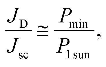 (where Pmin is the minimal light power and P1 sun is the light power under 1 sun condition), assuming a device current that is proportional with light intensity.19
It was further found that Voc plays an important role in the operation of OPVs under low light conditions since Voc follows a logarithmic relationship with light intensity (I) expressed by 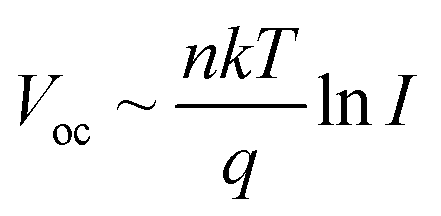 (where q is the elementary charge, k is the Boltzmann's constant, T is absolute temperature, and n is the diode ideality factor),20–22 which decreases with decreasing light intensity.23–25 Therefore, ensuring a high Voc under 1 sun, in conjunction with an ideality factor n close to 1, is a critical consideration to achieve high Voc and therefore high device performance under low light conditions.16 Yang et al. investigated the device performance of various OPV blend systems under both white LED and fluorescent illuminations, and also found that the devices with higher Voc values under 1 sun generally exhibit higher performance under low light (up to 13.76% at 500 lx, Fig. 1a).26 More recently, much effort has been made on enhancing Voc for indoor OPVs through controlling the donor–acceptor energetics, i.e. the effective bandgap which is the energy level difference between the lowest unoccupied molecular orbital (LUMO) of the acceptor and the highest occupied molecular orbital (HOMO) of the donor. Based on a deep-HOMO PDTBTBz-2Fanti donor and a PC71BM acceptor, You et al. obtained a high Voc of 0.817 V and an outstanding PCE of 23.1% under 1000 lx LED illumination, surpassing the other polymer:PC71BM blends investigated (Fig. 1a and Table 1).27 However, for fullerene-based blend systems, there is limited potential to further enhance the Voc value since the energy level of the fullerene acceptor cannot easily be adjusted and only the energy level of the polymer donor can be tuned. Nonfullerene acceptors (NFAs), on the other hand, offer more opportunities to deliver higher Voc due to more adjustable properties of both the donor and acceptor. For example, based on the PBDB-TF polymer donor, Cui et al. found that the ITCC acceptor, which has a higher effective bandgap (1.69 eV) than IT-4F (1.31 eV), results in higher Voc under both AM 1.5G illumination (1.1 V vs. 0.872 V) and indoor light conditions (0.962 V vs. 0.712 V at 1000 lx LED light) (Fig. 1b and Table 2).28 In addition to a higher effective bandgap, reducing energy loss (Eloss) is also an important consideration. Cui et al. synthesised a wider-gap NFA molecule IO-4Cl with a smaller Eloss of 0.6 eV in blend with PBDB-TF under AM 1.5 G illumination, compared to a PBDB-TF:ITCC blend which has a Eloss of 0.65 eV. As a result, the PBDB-TF:IO-4Cl cell exhibits a higher Voc of 1.1 V under 1000 lx LED light compared with the 0.962 V for the PBDB-TF:ITCC cell.17
 | ||
| Fig. 1 (a) Energy level diagram, J–V characteristics under 1 sun and LED 1000 lx illumination of the devices with different polymer:PC71BM blend systems. Reproduced from ref. 27 with permission from WILEY-VCH. (b) Energy level diagram, J–V characteristics under 1 sun of the devices with different PBDB-TF:acceptor blend systems and J–V characteristics of PBDB-TF:ITCC-based devices under LED with different light intensities. Reproduced from ref. 28 with permission from WILEY-VCH. (c) Energy level diagram, J–V characteristics under 1 sun and FL l000 lx of the devices with CD1:PBN-10 and CD1:ITIC blend systems. Reproduced from ref. 30 with permission from The Royal Society of Chemistry. | ||
| Device | Light source | V oc (V) | J sc (1 sun: mA cm−2) (LED: μA cm−2) | FF (%) | P out (mW cm−2) | PCE (%) |
|---|---|---|---|---|---|---|
| PDTBTBz-2Fanti:PC71BM (device A) | 1 sun | 0.903 | 14.4 | 53.3 | 6.93 | 6.9 |
| LED | 0.817 | 112.4 | 70.4 | 0.065 | 23.1 | |
| P3HT:PC71BM (device B) | 1 sun | 0.600 | 9.3 | 47.3 | 2.64 | 2.6 |
| LED | 0.498 | 73.7 | 71.9 | 0.026 | 9.4 | |
| PBDB-T:PC71BM (device C) | 1 sun | 0.764 | 11.8 | 67.2 | 6.06 | 6.0 |
| LED | 0.669 | 90.2 | 71.3 | 0.043 | 15.3 | |
| PTB7:PC71BM (device D) | 1 sun | 0.670 | 13.6 | 67.4 | 6.14 | 6.1 |
| LED | 0.569 | 87.6 | 69.3 | 0.035 | 12.3 |
| Device | Light source | V oc (V) | J sc (1 sun: mA cm−2) (LED: μA cm−2) | FF (%) | P out (mW cm−2) | PCE (%) |
|---|---|---|---|---|---|---|
| PBDB-TF:PC71BM | 1 sun | 0.945 | 12.9 | 67.1 | 8.43 | 8.43 |
| LED | 0.784 | 94.1 | 74.1 | 0.0547 | 18.1 | |
| PBDB-TF:ITCC | 1 sun | 1.10 | 14.3 | 64.3 | 10.3 | 10.3 |
| LED | 0.962 | 95.8 | 72.2 | 0.0665 | 22.0 | |
| PBDB-TF:IT-4F | 1 sun | 0.872 | 20.1 | 68.7 | 12.2 | 12.2 |
| LED | 0.712 | 113.0 | 78.0 | 0.0628 | 20.8 |
A wide gap close to 1.9 eV (ideal bandgap) is beneficial for matching the absorption spectrum with the indoor light sources and therefore obtaining superior photovoltaic performance,29 while the majority of the photoactive materials used in the indoor OPVs reported so far have a bandgap narrower than the optimal value. The above-mentioned PBDB-TF:ITCC and PBDB-TF:IO-4Cl blends with a decent bandgap and well-match absorption spectrum have demonstrated outstanding PCEs of 22.0% and 26.1% under 1000 lx LED illumination, respectively.17,28 Ding et al. recently reported an efficient all-polymer blend system with a bandgap over 1.9 eV, which is promising for indoor applications. The authors introduced a new class of polymer acceptors containing boron–nitrogen coordination bonds (B ← N), which possess suitable bandgaps with tuneable LUMO and HOMO energy levels.30 In particular, the polymer acceptor PBN-10 (which has a bandgap of 1.95 eV) in blend with the polymer donor CD1 (which has a bandgap of 1.93 eV) as the active layer exhibits a PCE of 26.2% under FL illumination at 1000 lx with a high Voc value of 1.14 V (Fig. 1c and Table 3). The high device performance of the new target-developed wide-gap materials illustrates the great potential of OPV devices for further performance enhancement under low light conditions.
| Device | Light source | V oc (V) | J sc (1 sun: mA cm−2) (LED: μA cm−2) | FF (%) | P out (mW cm−2) | PCE (%) |
|---|---|---|---|---|---|---|
| CD1:PBN-10 | 1 sun | 1.29 | 10.10 | 60.8 | 7.93 | 7.93 |
| FL | 1.14 | 120 | 66.2 | 0.091 | 26.2 | |
| CD1-ITIC | 1 sun | 0.91 | 16.39 | 58.3 | 8.69 | 8.69 |
| FL | 0.78 | 116 | 68.1 | 0.062 | 17.9 |
It was recently reported that the performance of OPVs under low light conditions can be improved through morphology optimisation of the active layer. Lee et al. found that the performance of a small molecular donor-based OPV system (BTR:PCBM) under low light can be improved by balancing the crystallisation and the phase separation of the active layer via solvent vapour annealing (SVA), obtaining an outstanding PCE (∼28%) among the fullerene based OPV devices under 1000 lx.31 In addition, the choice of transporting layers is also found to be crucial for achieving high-performance indoor OPVs. Ma et al. reported a high-efficiency indoor OPV device based on a polymer:nonfullerene system PM6:Y6-O with a band-aligned electron transporting interlayer (ETL) PDI-NO, which has a deep HOMO energy level with good hole-blocking properties. A high PCE of 30.1% was obtained with a high FF of 76% due to low leakage current and trap-assisted recombination in PDI-NO-based OPVs under 1650 lx LED illumination.9 Furthermore, OPVs based on ternary or quaternary blend systems are also a promising route for high-performing indoor PV applications.32 For example, by introducing a polymer donor PDTSTPD to a binary PCDTBT:PC71BM blend system, the efficiency is increased from 16.5% to 20.8% under 300 lx fluorescence light.33 This is due to the passivating effect of the PDTSTPD component on the shallow traps near the PCDTBT:PC71BM band edge, facilitating an enhanced hole mobility. Recently, Cho et al. introduced a third component Y-Th2 acceptor into a host PM6:Y6 nonfullerene blend system, achieving a PM6:Y-Th2:Y6-based ternary OPV device with a high PCE of up to 22.72% under LED light at 1000 lx. The addition of NFA Y-Th2 was found to broaden the absorption in visible light, adjust the energy level alignment between donor and acceptor and optimise the blend compatibility, allowing efficient charge-carrier transport in the active layer.34 Moreover, a quaternary OPV (Q-OPV) blend system comprising two polymer donors and two small molecule acceptors was demonstrated by Nam et al.35 Compared to the reference binary OPV system, this Q-OPV system has advantages of improved charge transfer processes from the donors to acceptors, increased Rsh and Voc values and well-aligned energy levels of the donors and acceptors. It was further found that higher Rsh can be achieved in thicker Q-OPV devices, resulting in increased FF and Jsc and thereby enhanced PCE with increasing the active layer thickness. Q-OPVs are also promising for semi-transparent and large area applications due to their high tolerance to variations in active layer thickness, which will be discussed further below.
In summary, high-performance indoor OPVs can be achieved by (a) optimising the bandgap of donors and acceptors to match the emission spectra of indoor light sources, thereby ensuring efficient light absorption; (b) targeting blend systems with a high Voc in conjunction with a low ideality factor; (c) targeting materials and device designs with sufficiently large shunt resistance and a low dark current; (d) optimising the materials and device processing conditions including the blend morphology and interlayers and (e) adopting suitable ternary/quaternary blend systems.
 | ||
Fig. 2 (a) J–V characteristics of an OPV device with a 4.0 cm2-large area under 1 sun and an LED illumination. Inset: a photograph of the 4![[thin space (1/6-em)]](https://www.rsc.org/images/entities/char_2009.gif) cm2 device. Reproduced with ref. 17 with permission from Springer Nature. (b) J–V characteristics of an 8-pixel module OPV device (red) with a total active area of 100 cm2 and a pixel (purple), respectively under FL at 300 lx. Inset: a photograph taken of this module. Reproduced with ref. 23 with permission from AIP Publishing. (c) Photographs, schematic and (d) J–V characteristics of 6 series-connected devices fabricated on a glass substrate and a flexible substrate. Reproduced with ref. 38 with permission from the American Chemical Society. cm2 device. Reproduced with ref. 17 with permission from Springer Nature. (b) J–V characteristics of an 8-pixel module OPV device (red) with a total active area of 100 cm2 and a pixel (purple), respectively under FL at 300 lx. Inset: a photograph taken of this module. Reproduced with ref. 23 with permission from AIP Publishing. (c) Photographs, schematic and (d) J–V characteristics of 6 series-connected devices fabricated on a glass substrate and a flexible substrate. Reproduced with ref. 38 with permission from the American Chemical Society. | ||
To further explore the potential of indoor OPVs toward future commercialisation, Lee et al. fabricated an 8-pixel module with an active area of 100 cm2 by spin-coating PCDTBT:PC71BM solution on a 14 cm × 14 cm substrate, generating a maximum power of 938 μW under FL at 300 lx (Fig. 2b).23,24 Arai et al. fabricated OPV modules with a total active area of 9.5 cm2 by connecting 6 cells in series based on the BDT-1T-ID:PNP blend system, obtaining a PCE of 15% with an output power of 111 μW cm−2 under 200 lx white LED light. Modules were also prepared on a flexible PEN substrate, showing a power output of 101 μW cm−2 under the same low light conditions.38,39 The authors further fabricated OPV modules based on the 1DTP-ID:PNP blend systems with a total active area of 9.6 cm2 on flexible PEN substrates, obtaining a flexible and large-area OPV device with a PCE of 17% under 200 lx LED light (Fig. 2c).26 These studies demonstrate the unique advantages of OPVs as a promising candidate for indoor PV applications with highly adjustable materials properties (e.g. colour, optical transparency) and device form factor (e.g. size, shape, flexibility), with outstanding potential for integration with a broad range of target applications.
A common strategy to achieve efficient semi-transparent OPVs under 1 sun illumination is to use a thin active layer film with near-infrared (NIR) absorbers to allow higher transmission in the visible light region.40 This strategy, however, is not suitable for indoor OPVs since the majority of indoor light sources nowadays are energy efficient and mainly emit in the visible region, thereby resulting in limited light absorbance and low PCE. To overcome the challenge, Yin et al. introduced a porphyrin-based donor P2, the absorbance of which has a valley in the region most sensitive to human eyes but with stronger absorption at the blue/red end, allowing high visible light transmittance and good colour rendering under indoor cold light sources. A semi-transparent P2:PC71BM OPV device was fabricated with an active layer thickness of 70–80 nm, showing a PCE of 10.7% under a LED illumination of 300 lx with an average visible transmittance (AVT) of 67% of the active layer.41 Nam et al. fabricated a semi-transparent quaternary OPV device with a whole device AVT of 13.7% by only reducing the thickness of Ag to 15 nm, whose active layer thickness is 170 nm, with an AVT of 48.3%. This semi-transparent OPV device had achieved a PCE of 14.64% under LED with 1000 lx (Fig. 3a).35
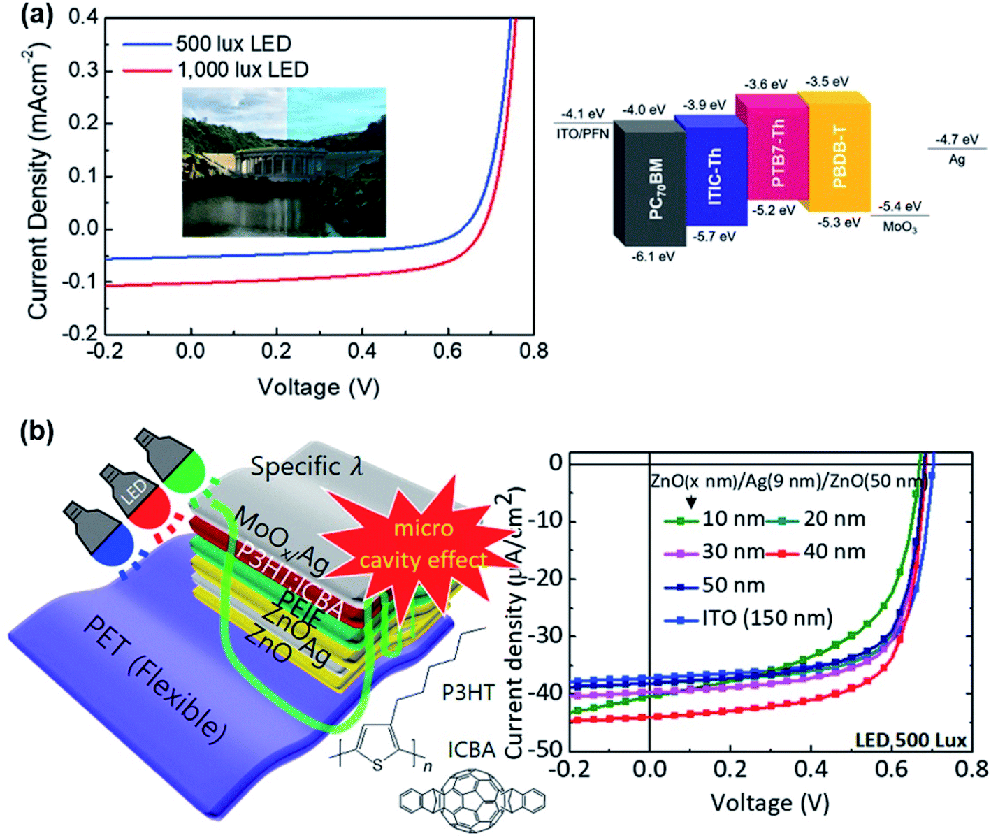 | ||
| Fig. 3 (a) J–V characteristics of a quaternary-OPV device under a LED illumination, and energy level alignment of the quaternary OPV device. Inset: a photograph taken with (right) and without (left) a quaternary OPV filter. Inset: a photograph taken with (right) and without (left) a quaternary OPV device. Reproduced from ref. 35 with permission from WILEY-VCH. (b) Schematic illustration and J–V characteristics of a flexible OPV structure with the ZnO–Ag–ZnO transparent electrode under indoor light illumination. Reproduced with ref. 42 with permission from Elsevier. | ||
The development of devices with high optical transmittance and mechanical flexibility is also an important consideration for indoor OPVs. An OPV device with a ZnO/Ag/ZnO (ZAZ) transparent bottom electrode was recently introduced by Lee et al.42 ZAZ electrode-based OPVs achieved transmittances up to 92% in the visible region and a sheet resistivity of 4.8 Ω sq−1, yielding a PCE of 12.3% under a LED lamp at 500 lx. The authors further fabricated a flexible OPV device with a ZAZ electrode, obtaining a PCE of 10.2% under a LED lamp at 500 lx with fairly good mechanical stability (with PCE dropping from 10.2% to 8% upon 400 cycling bends, Fig. 3b).
2.2 PPVs for indoor application
PPV cells have been one of the hottest topics in solar cells in recent years, achieving a record PCE over 25% for single-junction devices under standard solar irradiation, owing to the outstanding optoelectronic properties of perovskite semiconductors including strong optical absorption, high carrier mobility and lifetimes, and high tolerance to defects.43,44 The application of PPVs in low light applications was first reported by Chen et al.45 with an inverted device structure of PEDOT:PSS/MAPbI3/PCBM/TmPyPB/Ag, achieving a PCE of 27.4% for small area (5.1 mm2) devices and 20.4% for large area (5.44 cm2) devices under 1000 lx FL illumination, with promising long-term stability (maintained 97% of initial efficiency after 40 days under ambient indoor lighting with device encapsulation). Since then, the PCE of PPV devices under indoor light has been improved substantially, primarily driven by further optimisation of the fabrication process (in particular through engineering of the perovskite layer composition and interlayers) to achieve optimal control of the perovskite crystallinity, trap states and carrier dynamics. The recent progress on materials development and device engineering methods of PPVs for indoor applications is summarised in the following section.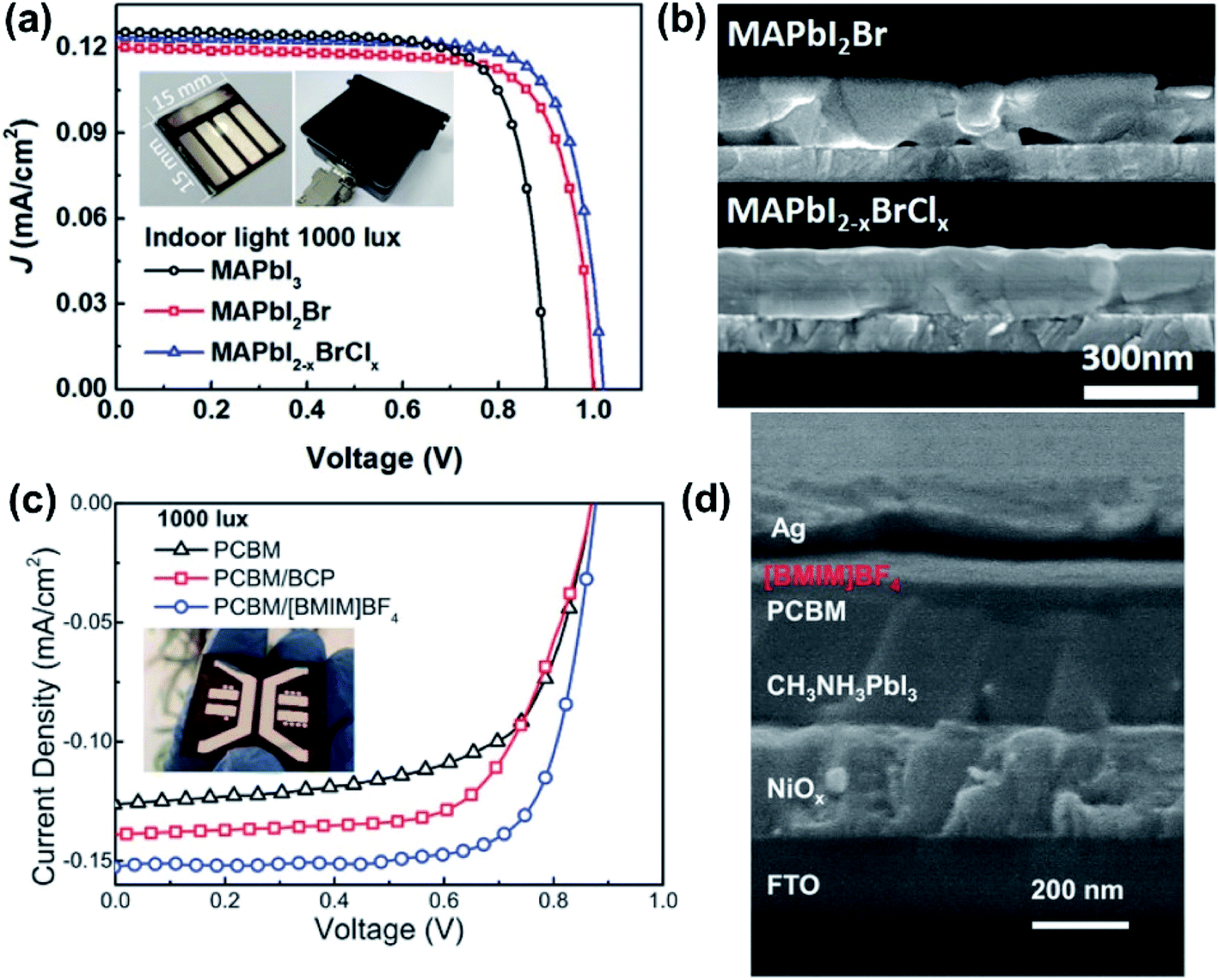 | ||
| Fig. 4 (a) J–V curves of the three groups of halide-engineered devices under 1000 lx FL light; inset shows the PPV device (1.5 × 1.5 cm2) and the test holder for 0.1 cm2 active area.51 (b) SEM cross-sectional views of MAPbI2Br and MAPbI2−xBrClx films.51 Reproduced with permission ref. 51. Copyright 2019, WILEY-VCH. (c) J–V curves of PPV based on PCBM, PCBM/BCP, PCBM/[BMIM]BF4 ETLs under 1000 lx; inset shows the device picture.57 (d) SEM cross-sectional views of [BMIM]BF4-based PPV layers.57 Reproduced with permission ref. 57. Copyright 2019, WILEY-VCH. | ||
In addition to bandgap optimisation, good film crystallinity and low defect density are also important considerations for PPVs in order to achieve efficient charge transport with long electron and hole-diffusion lengths. In particular, trap states could dominate PV performance under low light conditions, since there are not enough photocarriers to fill these traps, leading to inefficient charge separation at the interfaces and perovskite grain boundaries as well as high leakage current.53 Therefore, current strategies for performance enhancement of PPVs under low light have been mainly focused on compositional engineering in order to reduce the defect density of the perovskite materials, and through interfacial engineering in order to suppress the leakage current and improve the charge extraction at the interfaces.51,53,54
Dagar et al. used a SnO2/MgO double ETL in the PPV device to rectify the dark J–V curves by effectively reducing the number of pin holes and blocking the perovskite–electrode contact.55 A PCE of 26.9% under 400 lx LED illumination was achieved, representing a 20% enhancement compared to the device only employing a SnO2 layer. Lee et al. reported significantly improved performances of PPVs under 1000 lx FL light after replacing PTAA HTL with spiro-OMeTAD in a conventional device structure (resulting in an increased Pmax from 16.1 to 115.6 mW cm−2) and replacing PEDOT:PSS HTL with poly-TPD in an inverted device structure (resulting in an increased Pmax from 68 to 111.9 mW cm−2), which is attributed to the significantly suppressed dark current.56 Li et al. employed 1-butyl-3-methylimidazolium tetrafluoroborate ([BMIM]BF4) as the modification layer to passivate the surface trap-states of PC61BM/Ag and achieved a PCE of 35.2% under a 1000 lx fluorescent lamp (see Fig. 4c and d).57 Noh et al. reported a SnO2/ZnO bilayer-structured ETL, which not only possesses suitable energy band matching but also suppressed trap-assisted recombination at the MAPbI3 interface, realising a PCE of up to 37.2% under 1000 lx LED light.10 It was found that further optimisation of the fabrication process of PPV devices can also reduce the trap density at the perovskite/ETL or perovskite/hole transporting layer (HTL) interfaces. For example, PPV devices prepared with an atomic-layer-deposited compact TiO2 (c-TiO2) interlayer between the ITO and mesoporous TiO2 (m-TiO2) layers exhibit a decreased number of pin holes, resulting in improved device performance under both indoor and outdoor illumination conditions compared to devices employing TiO2 interlayers deposited by sol–gel spin coating and spray pyrolysis.58 A PPV device employing a two-step processed PCBM layer, where a thin diluted PCBM layer was first deposited to fill the traps of the perovskite films formed during the thermal annealing process, followed by a thick PCBM layer deposited on the diluted PCBM layer, was found to exhibit better performance than a device employing one-step processed PCBM ETLs.45
In summary, high-performance indoor PPV devices can be facilitated by careful compositional engineering to adjust the material bandgap to ∼1.9 eV, as well as optimisation of the materials and device processing routes and interfaces to achieve good perovskite crystallinity with a low density of defects.
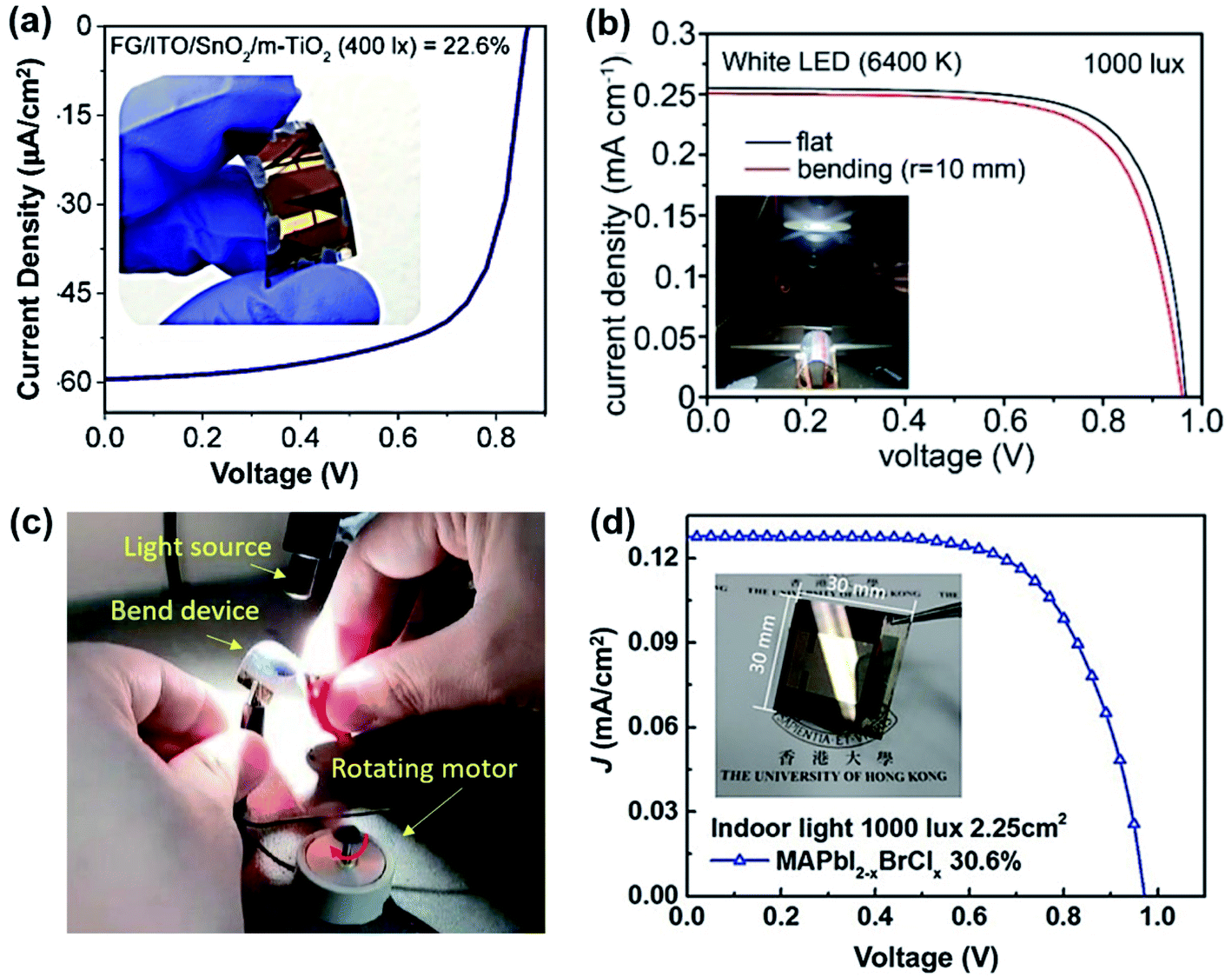 | ||
| Fig. 5 (a) J–V curve of the FG based device under 400 lx LED illumination; inset shows the photograph of a curved FG-PPV device. Adapted with permission ref. 66 under the CC BY-NC-ND license. (b) J–V curves of the flat and bent devices at a radius of 10 mm and the photo of the testing platform (inset).67 (c) Photo of the simulated experiment at 5000 lx for the flexible PPV device interconnected to the motor.67 Adapted from ref. 67 with permission from the American Chemical Society. (d) J–V curve of the MAPbI2−xBrClx base PPV device under 1000 lx FL light with a large area of 3 × 3 cm2 and active layer of 2.25 cm2. Reproduced with permission ref. 51. Copyright 2019, WILEY-VCH. | ||
For the fabrication of larger modules, more processing problems should be considered. A key consideration is to achieve high film uniformity over large-area substrates without pinholes or other inhomogeneity during the precursor solution drying and perovskite crystallisation processes. However, the crystallisation kinetics of perovskites are different on small and large area substrates, leading to multidirectional crystal growth of the precursor on a large-area substrate without control.68 To solve this problem, several approaches have been proposed, such as using anti-solvents to extract the solvents from the precursor solution and accelerate perovskite precipitation, expanding the precursor processing window (the time needed for perovskite material precipitation) by selecting mixed solvents with longer evaporation times and using chemical additives to control crystal growth.68–70 A 10 × 10 cm2 PPV module with a PCE of close to 18% has recently been demonstrated through the dynamic anti-solvent process.71 In addition, for large modules, inhomogeneity of the layer thickness across the substrate will affect the current and FF of the sub cells with the worst sub cell dictating the overall current and FF in the series-connected modules, which needs to be optimised delicately to ensure consistent distribution of each layer's thickness. With such optimisation, Rossi et al. manufactured a stable A4-size module (with an active area of 198 cm2) with PCE ∼ 6.6% under 1 sun and an outstanding PCE of ∼18% under l000 lx FL lighting.72
2.3 QDPVs for indoor application
QDs have been brought to the forefront of the development of high-definition television (HDTV) over the past 2–3 years as a more versatile alternative to organic LEDs with a higher colour gamut. As an immediately related technology, the development of QDPVs can directly benefit from QD LEDs as a highly promising PV technology73,74 that suffer no compromise between high theoretical efficiency, stability and low cost, showing excellent ambient tolerance after QD surface passivation and band alignment.75,76 Compared with perovskites, conventional bulk semiconductors and organic semiconductors, QDs possess a low photon energy threshold for multiple exciton generation, which enables QDPVs to go beyond the Shockley–Queisser (SQ) limit.77,78 For free-standing QDs or colloidal dispersion, due to the spatial confinement of the QDs, electron–hole pairs interact strongly through the Coulomb potential, which enables electron–hole pairs to remain as excitons, not free-carriers; furthermore, free carriers can only form upon dissociation of the excitons.79 QDs can enhance the efficiency of the electron–hole pair multiplication processes where the excess photon energy can be used to produce additional electron–hole pairs, instead of loss as dissipated heat.80 Meanwhile, the highly tunable bandgap of QDs facilitates efficient energy harvesting in the near to short-wave infrared region of the solar spectrum.81 However, the current QDPV 1 Sun efficiency is still lower than those of OPVs and perovskite solar cells which is mainly due to the complicated material synthesis process and a vast number of defect states generated during device fabrication. While QDPVs usually exhibit only modest PCE (around 13%)82,83 compared to OPVs and PPVs under 1 sun condition, they have strong potential in achieving high device performance under low light conditions, considering the highly tuneable bandgaps of QDs by changing their size,84,85 making them an efficient low light energy harvester.To investigate the potential of QDPVs for indoor applications, Hou et al. demonstrated the first indoor QDPV device based on lead sulfide (PbS) quantum dots.11 The results show that a maximum PCE of 19.5% can be achieved under FL illumination from 200 lx to 2000 lx (see Fig. 6a), significantly higher than the record PCE of QDPVs under 1 sun (∼13.8%).82 The authors further demonstrated the feasibility of QDPVs in powering indoor-light-sensor networks. As shown in Fig. 6b, the QDPV matrix can readily charge the integrated capacitor (inset) under 10000 lx, under which the infrared sensor can work successfully as indicated by the dynamically tracked sensor process (Fig. 6c). To investigate the stability of QDPVs under typical indoor operating environments, the evolution of their device performance under continuous low light exposure (1000 lx insolation) in the ambient atmosphere without encapsulation was recorded. As shown in Fig. 6d, minimal degradation in the device performance of QDPVs was observed upon 1800 hours of continuous light exposure. The practical application and long lifetimes demonstrated in the work of Hou et al. are credible evidence of the high commercialisation potential of indoor QDPVs.
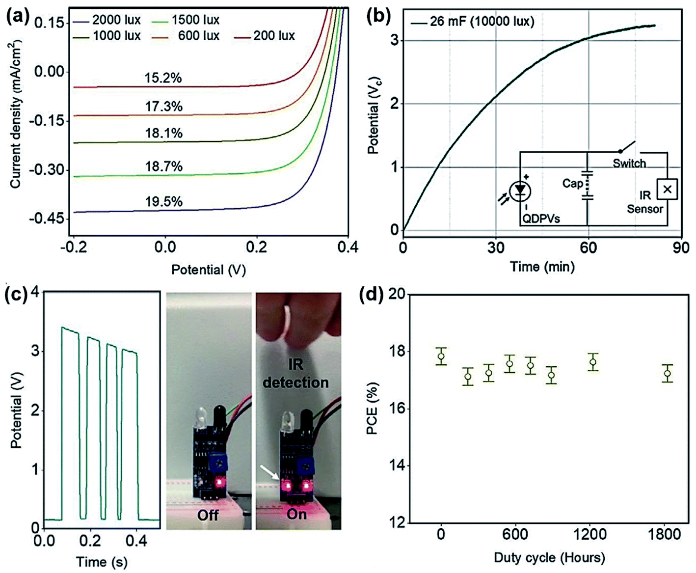 | ||
| Fig. 6 (a) J–V curves and PCE values of the QDPVs at different room light irradiance levels. (b) Capacitor charging curve under 10000 lx light. Inset describes an integrated circuit of QDPVs, capacitors and an IR sensor. (c) Snapshots and transient signals from the IR sensor. (d) The unencapsulated QDPV PCE stability performance under 1000 lx insulation for a continuous 1800 h exposure. Reproduced from ref. 11 with permission from WILEY-VCH. | ||
It should be noted that the studies on QDPVs for low light applications are still limited in the literature. While the outstanding low light performance of QDPVs achieved in the work above is a good demonstration of the potential of indoor QDPVs, further investigations are urgently needed in order to optimise the device performance via QD materials and size engineering. Nevertheless, given the successful commercialisation of QD based HDTV as well as the fast development of QD ambient lighting, QDPVs should be considered a competitive candidate for future indoor PV applications. In particular, since there is no scientific barrier between the red QD LEDs and QDPVs, the established LED device processing technologies and the excellent compatibility of QDs with flexible, large area and transparent electrodes, are expected to be easily implemented for indoor QDPVs. In addition, QD thermophotovoltaic devices can be alternative promising candidates for harvesting indoor energy into electrical power by utilising a small bandgap semiconductor that absorbs the low-energy infrared photons from radiated thermal energy and using asymmetric contacts to the absorber (such as QD layers) to transfer net electrical power to load.86
To compare the optimal bandgap for outdoor and indoor PVs as well as the state-of-the-art of different indoor PV technologies, a plot of the SQ-limited PCE as a function of optical bandgap, as well as plots of device PCE and Pmax as a function of bandgap and illuminance, is shown in Fig. 7, with the device parameters of several representative outstanding PV cells summarised in Table 4. Fig. 7a exhibits an optimal bandgap of ∼1.9 eV for indoor PV under typical indoor light sources, in comparison to the range of 1.1 to 1.4 eV under AM 1.5 G condition.87Fig. 7b and c show that a larger energy bandgap closer to 1.9 eV can result in a higher device PCE and Pmax for OPVs, PPVs and QDPVs under low light, with indoor PPVs currently exhibiting the highest PCE and Pmax. It should be noted, however, that in addition to an optimal bandgap, device architecture and type of materials also play an important role in device performance as evidenced by the superior PCE of the PM6:Y6-O blend with the PDI-NO interlayer and MAPbI3 PPVs with the SnO2/ZnO double ETL, and by the big performance difference between BTR:PC71BM and PBDB-TF:PC71BM. It is expected that the device performance of all three types of indoor PV technologies will continue to improve significantly with the rapid advances both in the materials and device design.
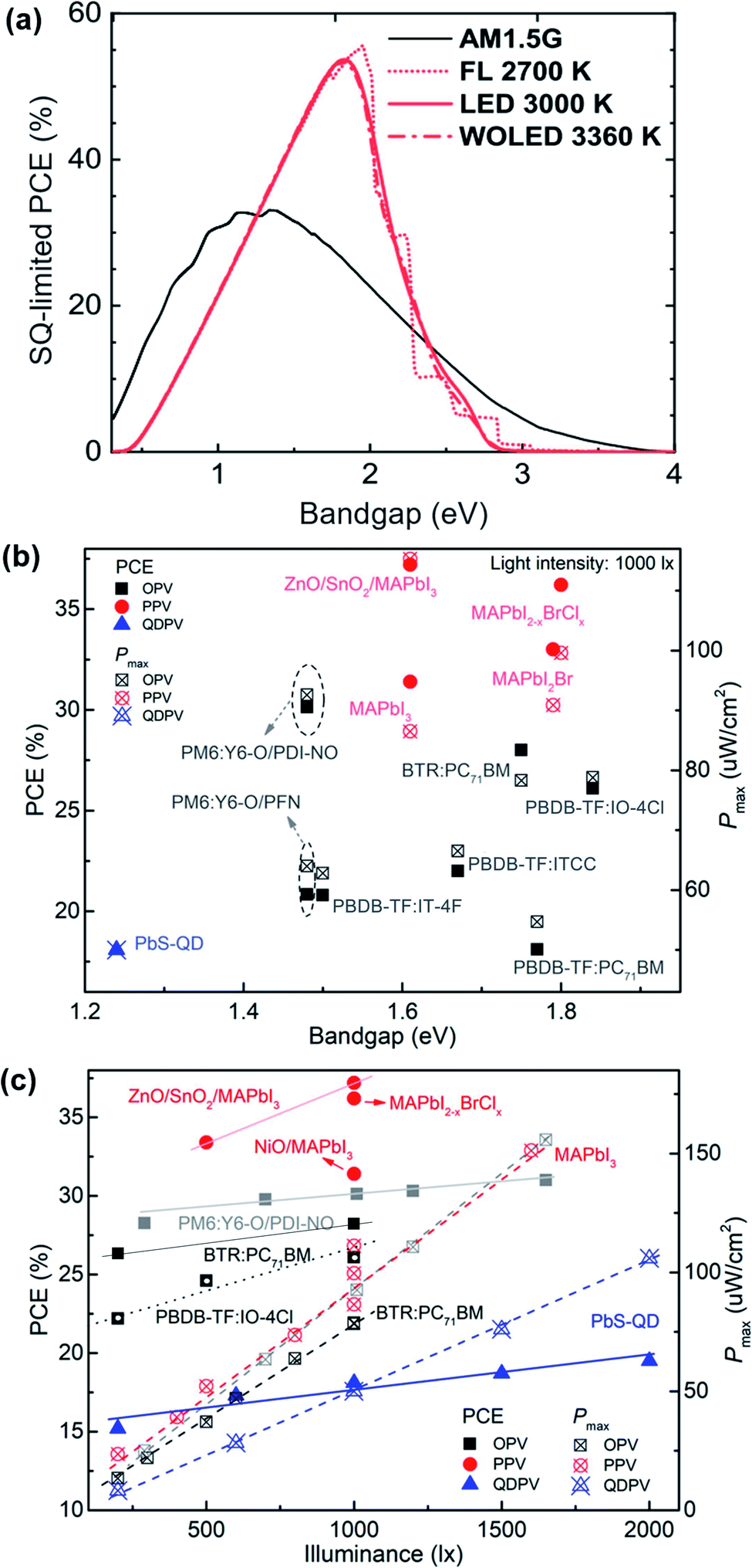 | ||
| Fig. 7 (a) The Shockley–Queisser (SQ) limited PCE vs. bang gap for different white light sources. The illuminance of artificial light sources is taken to be 300 lx. Adapted from ref. 87 with permission from The Royal Society of Chemistry. (b) PCE and Pmax of PV cells vs. acceptor bandgap under 1000 lx LED light illumination. The bandgap data was calculated from the device EQE edge of the blend film. (c) Plot of PCE and Pmax of different types of indoor PV cells with increasing light intensity. Data from ref. 9, 17, 28 and 31 for OPVs, ref. 10, 51 and 53 for PPVs and ref. 11 for QDPVs. | ||
| Device | Light source at 1000 lx | V oc (V) | J sc (μA cm−2) | FF (%) | P max (μW cm−2) | PCE (%) | Ref. |
|---|---|---|---|---|---|---|---|
| BTR:PC71BM | FL | 0.79 | 133.1 | 75.2 | 78.3 | 28 | 31 |
| PBDB-TF:IO-4Cl | LED | 1.1 | 90.6 | 79.1 | 78.8 | 26.1 | 17 |
| PM6:Y6-O/PDI-NO | LED (1010 lx) | 0.83 | 147 | 76 | 96.2 | 30.1 | 9 |
| MAPbI2−xBrClx | FL | 1.028 | 126.2 | 76.8 | 99.6 | 36.2 | 51 |
| MAPbI3−xBrx | LED | 0.82 | 170.8 | 68.8 | 96.4 | 34.5 | 52 |
| ZnO/SnO2/MAPbI3 | LED | 0.98 | 157.6 | 72 | 115.3 | 37.2 | 10 |
| PbS-QD | FL | 0.34 | 213.3 | 69 | 50 | 18.1 | 11 |
3 Scientific and industrial challenges
3.1 Standards of PV measurements
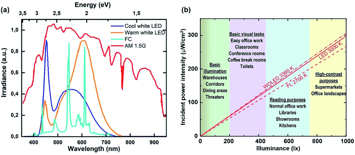 | ||
| Fig. 8 (a) Spectral emission of common ambient light sources and the solar spectrum at AM 1.5G. Reproduced from ref. 89 with permission from the American Chemical Society. (b) Incident power intensity vs. illuminance for selected light sources. Reproduced from ref. 87 with permission from The Royal Society of Chemistry. | ||
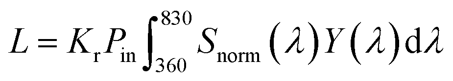
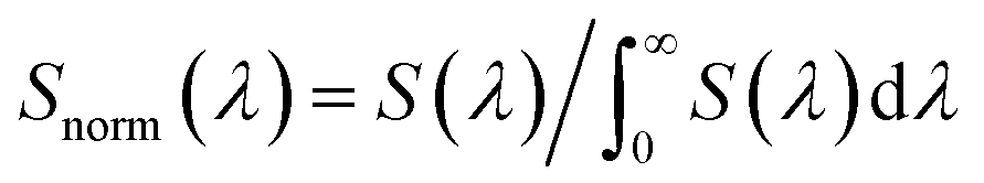
Once the light source is decided, accurate light intensity calibration is a further consideration. Other than the normal irradiance measurements (mW cm−2) for PCE calculation, illuminance measurements, typically by using a lux meter, are also required as they describe brightness based on human eye perception which is wavelength dependent. To convert irradiance into illuminance, a wavelength-weighted factor – luminosity factor Y(λ) is involved in the calculation which describes human eye responses to a particular wavelength.2 The equation of the conversion is shown in eqn (1) and (2).
 | (1) |
 | (2) |
Instead of performing accurate measurements of the spectrum and intensity of the indoor light source, Hamadani et al. proposed using a calibrated reference cell to test the light intensity levels for a given reference spectrum of the indoor light source, which is similar to the routine calibration of 1 sun measurements currently adopted in most laboratories. By this method, researchers are able to calibrate the light intensity levels simply by using the reference cell, without the need to measure the absolute irradiance of the indoor light sources or the absolute quantum efficiency of the PV devices.90
It is common to observe hysteresis in the J–V scans for many types of PPV devices, where the current for a given voltage is dependent on the scan direction (forward or reverse) and scan rate. Chen et al. conducted an intense study on the variation of indoor performance of dye-sensitised PV devices, which is found to suffer from hysteresis, involving 15 research groups from around the world.91 While there are currently very few reports on the hysteresis of PPV devices under low light conditions, the findings of Chen et al. suggest that the hysteresis of PPV devices could be more serious under low light conditions and a low scan rate may be required, and stabilised power generation measurements (Pmax over time) would be a more accurate method to probe Pmax.
Even when the indoor light sources for PV testing have been calibrated, the accuracy remains unclear, since there is no third-party calibrated reference to calibrate the light intensity similar to that for 1 sun J–V measurements. Therefore, it is important to perform integration of the EQE spectrum to the indoor spectrum as a check of the obtained Jsc value. However, such a check is rarely seen in the literature for indoor PVs.17,28 We thereby suggest that this integration should be reported in the future.
3.2 Stability
Stability remains a key consideration for the commercialisation of emerging solar cells. While significant research effort has been dedicated to understanding the degradation mechanisms and enhancing the long-term stability of OPV, PPV and QDPV devices under high light (e.g. AM1.5G) conditions,47,92,93 there are very few studies investigating their degradation behaviour under low light conditions to date, resulting in a limited understanding of their degradation mechanisms and hence a lack of materials and device design rules to achieve long term environmental stability. The very different environmental stress factors associated with low light conditions (e.g. lack of elevated temperatures, intensive light soaking, thermal cycling and weathering) suggest that the degradation of OPVs and PPVs under low light may be dominated by different mechanisms under high light conditions. In this section, we summarise the very recent research efforts in the stability studies of indoor OPV and PPV devices and discuss our perspectives on their degradation mechanisms under low light conditions, as well as potential strategies to address these mechanisms to enhance their long-term stability. Since QDPVs have shown excellent stability compared to OPVs and PPVs, but a comprehensive stability study of their environmental tolerance, such as moisture, heat, mechanical damage and long-time benchmark light soaking is seldom reported in the PV society, the stability of QDPVs under low light conditions is not included in this review.Photochemical stability. Photochemical degradation has been widely established as a major degradation pathway for the outdoor application of OPVs. The rapid degradation of device performance is typically triggered by a degradation of the donor and/or acceptor materials driven by the combined exposure to light and molecular oxygen, with the formation of singlet oxygen and superoxide ions, both identifying degradation mechanisms.94–96 In contrast, the photochemical degradation of OPV devices under low light conditions remains significantly underexplored. Yin et al. compared the degradation kinetics of unencapsulated PCDTBT:PC71BM devices under outdoor (AM1.5G) and indoor (300 lx LED) conditions in air (Fig. 9a), and found that the devices under low light exhibit remarkably similar degradation kinetics to those under high light, albeit with a slightly slower rate (a 20% PCE decrease under low light and a 30% PCE decrease under high light after 180 min).33 Considering the >1000 fold difference in light intensity under low light and high light conditions, the findings of Yin et al. suggest that the photochemical degradation of OPV devices can be triggered by very low levels of illumination, resulting in a relatively weak dependence of device photochemical stability on light intensity, which is not predictable from the accelerated lifetime testing methods currently widely established for stability studies under high light conditions (e.g. predicting device lifetime by a factor of intensity multiplication), and requires significant further investigation. To avoid oxygen-induced photochemical degradation of OPV devices, a general strategy is to encapsulate the devices by using a glass or plastic layer to protect the devices from the ingress of oxygen. However, glass-based encapsulation may significantly increase the manufacturing cost, while the relatively low-cost plastic-based encapsulation is generally less effective such that it can only partially impede oxygen diffusion. The development of an effective encapsulation technology with a low fabricate cost is still a substantial challenge for merging indoor PV technologies. Apart from oxygen-induced photochemical degradation, intrinsic chemical reactions of the constituent materials (without the involvement of oxygen) are an additional degradation pathway for indoor OPVs. For example, Wang et al. have recently reported that the interfacial chemical reaction between the PEDOT:PSS HTL and the ITIC NFA (revealed by Raman spectroscopy) can cause the degradation of PBDB-T:ITIC-based OPVs in an ambient indoor environment (Fig. 10a and b). This degradation mechanism is found to be effectively mitigated through a passivated MoO3 layer,93 suggesting that the development of suitable interlayers with excellent compatibility with the rapidly advancing materials and device designs of indoor OPVs is also an important consideration to ensure their long term stability.
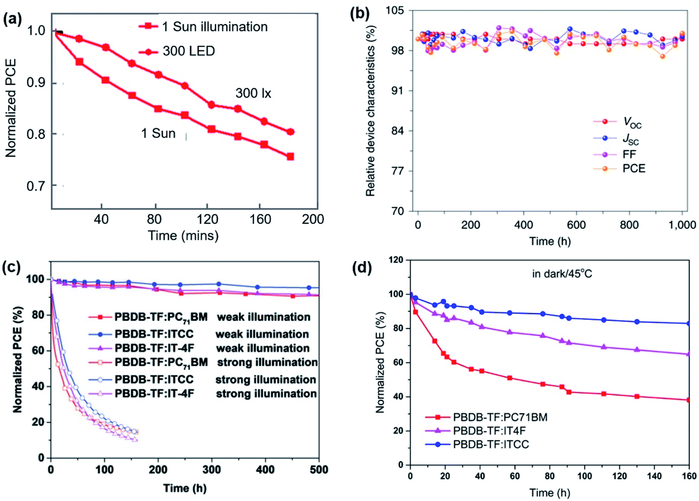 | ||
| Fig. 9 (a) The stability of unencapsulated PCDTBT:PC71BM cells under 1 sun and LED. Adapted from ref. 33 with permission from The Royal Society of Chemistry. (b) Photovoltaic characteristics of an encapsulated PBDB-TF:IO-4Cl OPV device as a function of time under continuous indoor light illumination. Reproduced from ref. 17 with permission from Springer Nature. (c) The stability of three encapsulated OPV cells under continuous weak and strong illumination,28 and (d) the thermal stability under 45 °C in dark.28 Reproduced from ref. 28 with permission from WILEY-VCH. | ||
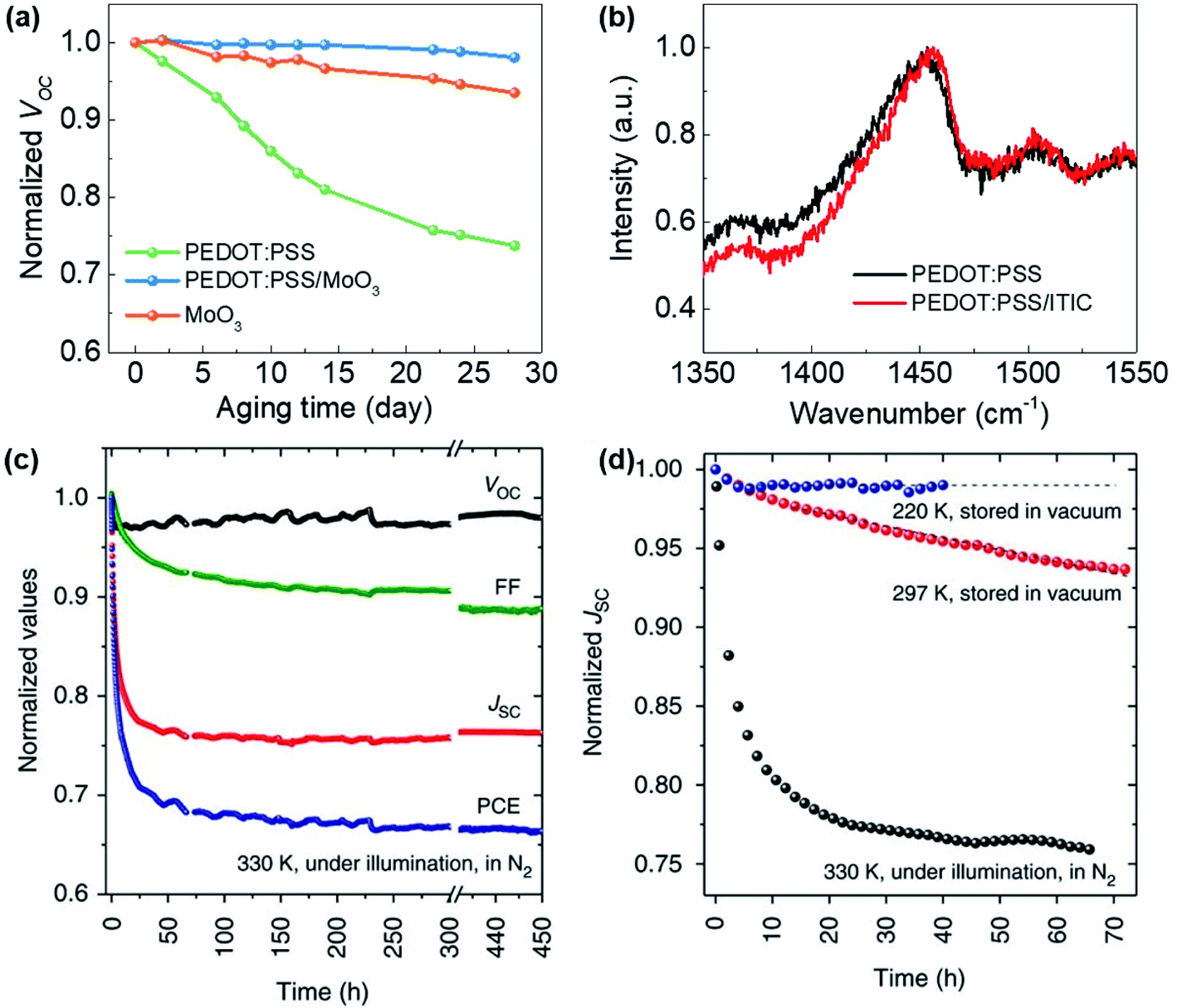 | ||
| Fig. 10 (a) The normalised Voc measured under 1 sun as a function of aging time.93 (b) Raman spectra measured for the pure PEDOT:PSS layer and the bilayer PEDOT:PSS/ITIC. Adapted from ref. 93 with permission from WILEY-VCH. (c) Evolution of Voc, FF, Jsc and PCE of optimised PCE11:PCBM solar cells measured under continuous 1 sun in a N2 atmosphere for 450 h.97 (d) Evolution of Jsc of optimised PCE11:PCBM solar cells measured at different temperatures. Reproduced from ref. 97 under a Creative Commons Attribution 4.0 International License. | ||
Strong illumination and high temperature. “Burn-in” behaviour can be observed when OPV devices operate in inert atmospheres under a continuous illumination, which represents a rapid drop of device performance within the first tens to hundreds of hours, further followed by a moderate decrease of device performance in the longer term.92 Li et al. demonstrated a strong burn-in degradation in PCE10:PCBM-based devices (Fig. 10c) under outdoor conditions, which is attributed to the demixing of the donor and acceptor phases caused by the low miscibility between the donor and acceptor. Notably, burn-in degradation due to spontaneous phase separation in the mixed amorphous regimes is found to occur at room temperature (Fig. 10d) and even in the dark.97 This study therefore shows that spinodal demixing of the active materials may be a critical issue for the stability of OPVs under low light conditions, which can be effectively mitigated by ensuring good miscibility and compatibility between the donor and acceptor. Cui et al. investigated the photostability of PBDB-TF:IO-4Cl devices under low light conditions, and found that the cell maintained its initial efficiency after a 1000 hour illumination period under indoor light as shown in Fig. 9b.9 The authors further compared the photostability of PBDB-TF:PC71BM, PBDB-TF:ITCC and PBDB-TF:IT-4F devices under indoor light at different intensities. The results reveal a strong dependence of the device degradation behaviour upon light intensity, with the devices under weak illumination exhibiting significantly higher stability, retaining 90% of their initial efficiencies after 500 hours of illumination (Fig. 9c).28 In contrast, the cells under strong illumination exhibit strong “burn-in” behaviour, losing more than 70% of their initial PCE within the first 100 hours, partially caused by a mild thermal stress (∼45 °C) during illumination as revealed by dark thermal stability tests (Fig. 9d).28 While the lack of intensive light soaking and elevated temperatures may facilitate the long term stability of OPV devices under low light conditions, the development of OPV materials with improved intrinsic stability against light soaking stress, as well as OPV blends with good morphological stability against thermal stress, is still an important consideration to ensure the long term stability of OPV devices under low light conditions.
Humidity. Since indoor OPVs may operate in an environment with high humidity, moisture-induced degradation can be a major degradation pathway for indoor OPVs, especially unencapsulated devices. It was reported that some top electrode materials such as calcium and aluminium can react with moisture in ambient air, forming bubbles and extensive voids at the top electrode/active layer interface, which spreads inward from the edge of devices over time upon exposure to relative humidity (RH) of 75%, causing degradation in device performance. The use of PEDOT:PSS as an HTL may also result in the degradation of indoor OPVs owing to its hygroscopic nature. Moisture induced degradation can be effectively mitigated by encapsulating the devices after fabrication, using moisture stable electrodes such as silver as well as replacing PEDOT:PSS or using additives in PEDOT:PSS.98 While it is reasonable to expect that indoor OPVs may share similar degradation mechanisms with outdoor OPVs under moisture conditions, further investigations are required in order to fully understand the moisture stability of indoor OPVs.
Perovskite layer. The perovskite photoactive layer plays a crucial part in the long-term stability of indoor PPVs. It has been established that the stability (under ambient/inert, dark/light, thermal/room-temperature conditions) of the perovskite layer can be significantly enhanced through composition engineering of the cation and anion elements, as well as through processing additives, antisolvent engineering and defect management.99
For example, it has recently been demonstrated that triple-halide tailored MAPbI2−xBrClx PPV devices can sustain over 95% of their initial efficiency under continuous light soaking under 1000 lx FL light for over 2000 h,51 while MAPbI3 and MAPbI2Br reference devices undergo significant degradation. This is due to the key role of the small Cl− ions in causing the shrinkage in the perovskite crystal lattice and further retarding ion migration and halide segregation. To obtain a stable perovskite phase, the adoption of mixed cation perovskites or inorganic perovskites has been established as a promising strategy under 1 sun condition,49,50 which may be also effective in the stability enhancement of indoor PPVs.100,101 Singh et al. reported that the Cs-tuned Csx(FA0.83MA0.17)(1−x)Pb(I0.83Br0.17)3 (where x is the mole fraction of Cs) perovskite devices can achieve an optimal PCE of ∼17% under AM1.5G condition when x = 0.05 and should also obtain decent device performance under low light conditions considering its extraordinary stability in the ambient atmosphere.101 This mixed-halide PPV device showed no significant degradation in device performance upon exposure to ambient air under dark conditions with RH 20–35% (see Fig. 11a) for 18 weeks. This enhanced stability was found to originate from the absence of impurity phases after addition of Cs, in conjunction with improved perovskite crystallinity as indicated by XRD analysis (inset of Fig. 11a).
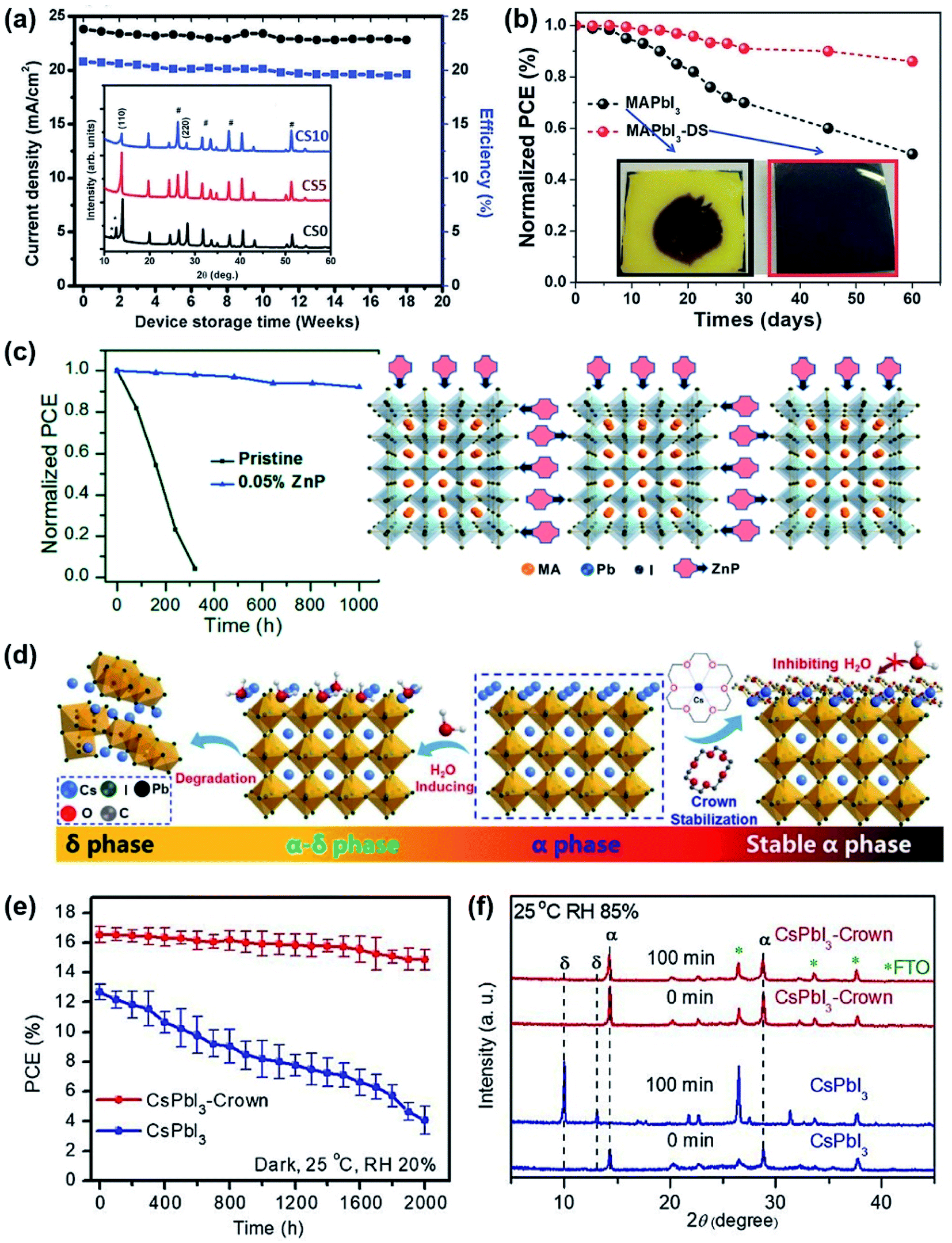 | ||
| Fig. 11 (a) Long term stability in device efficiency and current density with respect to device storage time in weeks under ambient conditions with RH 20–35%. The inset is the XRD of a Cs-tuned perovskite with Cs concentration x = 0 (Cs0), 0.05 (Cs5) and 0.1 (Cs10). Adapted from ref. 101 with permission from WILEY-VCH. (b) The stability measurements of the MAPbI3 and MAPbI3-DS devices exposed to ambient air at 35% humidity in the dark. Inset displays the photograph of the perovskite films after being stored for 60 days at the same condition. Reproduced from ref. 59 with permission from WILEY-VCH. (c) The stability measurements of the pristine and 0.05% ZnP-encapsulated MAPbI3 devices (85 °C, RH 45%) and the structure of perovskite encapsulated by ZnP. Adapted from ref. 102 with permission from the American Chemical Society. (d) Schematic illustration of Crown passivating the surface of α-CsPbI3, compared to the phase transition from α-CsPbI3 to δ-CsPbI3.100 (e) Storage stability of unencapsulated CsPbI3-Crown and CsPbI3 devices in a chamber with constant temperature and humidity.100 (f) XRD patterns of CsPbI3-Crown and CsPbI3 films in the ambient atmosphere at ∼RH 85% with different aging times.100 Reproduced from ref. 100 with permission from The Royal Society of Chemistry. | ||
Furthermore, processing additive engineering is also found to be an effective strategy in enhancing the stability of PPVs owing to their positive impact on perovskite crystallinity and morphology. For example, it was found that when a dimethyl sulfide (DS) additive is introducing into MAPbI3, the resulting PPVs had exhibited higher tolerance to oxygen and humidity, showing little degradation after 60 days (under dark ambient conditions, RH ∼ 35%, without encapsulation), while significant degradation is seen in pure MAPbI3 films as indicated by loss of absorbance (film yellowing, see Fig. 11b).59 This is due to the reaction of DS with Pb2+ to form a chelated intermediate, which further slows down the perovskite crystallisation rate to form large grain size and good crystallinity. Li et al. embedded the monoammonium zinc porphyrin (ZnP) compound into the MA+ lead iodide perovskite film and the resulting PPV devices showed enhanced moisture and thermal stability retaining over 90% of initial efficiency after 1000 h at 85 °C and 45% relative humidity in a N2 atmosphere (Fig. 11c).102 The significantly improved stability is attributed to the molecular encapsulation effect, where ZnP compounds were found to be attached on the surface of the perovskite nucleus, thereby mediating the crystallisation process and passivating the defects at the perovskite grain boundaries (Fig. 11c). Similarly, Chen et al. proposed a surface passivation method of drop-casting an 18-crown-6 ether (Crown) film on the CsPbI3 film surface.100 As shown in Fig. 11d, pristine α-phase CsPbI3 has high sensitivity to humidity, transferring to the α-δ- or δ-phases with H2O molecules attacking the surface. After introducing the Crown molecules, whose inner cavity can bond strongly and selectively with Cs+ ions, the surface defects can be passivated. Simultaneously, the Crown-terminated CsPbI3 exhibits a methylene (–CH2) outer structure on the surface, helping to enhance the moisture tolerance and thus inhibit the phase transformation. The device stability tests (Fig. 11e) show that the obtained high-quality CsPbI3-Crown devices had maintained ∼90% of their initial PCE for up to 2000 h without encapsulation (under dark, 25 °C, RH 20%), while reference CsPbI3 devices had lost ∼65% of their initial performance, dropping to only 4.7% after 2000 h under the same degradation environment. Under a harsher degradation condition with RH increased to 85%, the CsPbI3-Crown device can still maintain a stable α phase with very little δ phase emerging in the XRD pattern over 100 min (Fig. 11f), compared to the reference CsPbI3 films where most of the α phase had transferred into the δ phase. The emerging molecular and surface encapsulation methods of the perovskite layer therefore provide a promising new route for the commercialisation of efficient and stable indoor PPVs.
ETL and HTL. ETL and HTL also play a critical role in the stability of PPV devices. The widely used spiro-OMeTAD HTL in PPV devices usually requires additives to enhance device performance, while the common dopant lithium bis(trifluoromethanesulfonyl)imide (Li-TFSI) is hygroscopic resulting in high sensitivity to moisture. Pham et al. proposed to replace the Li-TFSI with the more hydrophobic alkaline-earth TFSI additives, such as Mg-TFSI2 and Ca-TFS I2, which can enhance moisture-resistance of the HTL layer and help to maintain 83% efficiency of the unencapsulated devices after aging in ambient air (RH 55–70%) for 193 days.103 To counter the stability related problems of HTL, a low-cost dopant-free 2,3-bis(4′-(bis(4-methoxyphenyl)amino)-[1,1′-biphenyl]-4-yl)fumaronitrile (TPA-BPFN-TPA) HTL with a water repellent property (contact angle of 112°) was recently developed.104 The TPA-BPFN-TPA-based PPV devices not only exhibited significantly improved device performance compared to spiro-OMeTAD-based PPV devices under low-light conditions (30% PCE at 1000 lx), but also improved device moisture stability under dark conditions with RH = 70% (PCE dropped from 18.4% to 8% in 100 h vs. 16.5% to 5% in 40 h). Jagadamma et al. developed an ultrathin HTL based on solution-processed NiO nanoparticles instead of PEDOT:PSS for indoor PPV devices, achieving a PCE of 23% under compact fluorescent lighting (0.32 mW cm−2).105 After 3.7 months under ambient air conditions (in the dark, RH ∼ 40%), the perovskite layer on the NiO HTL still retained its initial black-brown colour while the ones on PEDOT:PSS turned yellowish implying a severe loss of absorbance. The above mentioned (in Section 2.2.1) SnO2/MgO55 and PCBM/[BMIM]BF4 (ref. 57) based PPV devices, which exhibited higher PCEs than their reference devices under low light, also showed improved stability due to ETL/interlayer modification which leads to efficient passivation of surface trap states and less permeation of moisture and oxygen into the perovskite layer. Upon storage in air under dark for 107 days without encapsulation, the SnO2/MgO ETL/interlayer based MAPbI3 PPV devices maintained 68% of their initial efficiency, whereas those with only a SnO2 ETL maintained 53% after undergoing the same degradation period. The XRD patterns of the MAPbI3 films covered with PCBM/[BMIM]BF4 exhibited a pure MAPbI3 phase after 190 h of aging, while the PCBM/BCP-covered perovskite film displayed an additional peak in the XRD pattern corresponding to the formation of PbI2, implying a partial decomposition of MAPbI3 due to the invasion of moisture and oxygen. To further increase the water resistance, Sidhik et al. proposed to insert a hydrophobic PbS QD layer between the perovskite layer and HTL. Compared with the significantly degraded reference MAPbI3 devices after 10 days under dark ambient conditions with higher humidity of 70%, the devices utilising a PbS QD barrier layer showed less degradation (retaining 76% of their initial efficiency) after being stored for 60 days under the same environmental conditions.106
Top electrode. The commonly used metal electrodes (Au and Ag) for PPV devices are also important factors contributing to device degradation due to the diffusion of Au and reactivity of Ag with halide ions,47 which is also expected to exist in indoor PPVs. For better compatibility with indoor IoT application, alternative low-cost and nonreactive substitutes such as hydrophobic and abundant carbon-based materials were explored as reviewed in the literature.107 The carbon-based PPV devices show superior stability than the metal–electrode devices under both moisture and high-temperature environments. Although the carbon materials usually exhibit lower conductivity, the resulting PPV device with a carbon electrode still generates decent Pmax under low light intensity.56
3.3 Ecotoxicity
Since low light PVs are mainly targeting indoor and portable applications (IoTs, household products, wearable electronics and biomedical devices), ecotoxicity is a vital consideration for their materials and device design, and toxic/harmful elements should be avoided or properly controlled in order to minimise their ecotoxicity and meet the relevant safety regulations (e.g. RoHS) for their commercialisation. While there are relatively less concerns over the ecotoxicity of OPV devices (e.g. the use of heavy-metal atoms in the donor and acceptor materials17,28,108 with limited risk of chemical leach), ecotoxicity is a more serious consideration for the commercialisation of PPV and QDPV devices. A recent research study revealed that the Pb from halide perovskites is more harmful than initially expected, and is 10 times more bioavailable than other sources of lead contaminants that already exist around human life.109 Therefore, lead-free perovskites (e.g. Sn-, Ge- and all-inorganic based) and QDPVs (e.g. AgBiS2-based)110 are more desirable than their lead-based counterparts for low light applications.46,111 It should be noted, however, that lead-free PV devices typically possess lower performances and therefore still require substantial further development. To mitigate this issue, Li et al.112 developed an on-device lead sequestration strategy based on lead-based PPVs to effectively prevent the leakage of lead in order to minimise their ecotoxicity (Fig. 12a). The authors deposited transparent P,P′-di(2-ethylhexyl) methanediphosphonic acid (DMDP) outside the FTO glass to absorb Pb and an opaque ethylenediamine tetra (methylene phosphonic acid) (EDTMP) layer as Pb-sequestrating material on the device back side, which can together absorb 96% of Pb leaked upon device damage. These layers do not impact device performance and stability as indicated in Fig. 12b and c. Furthermore, the development of environment friendly materials and green fabrication procedures is also an important consideration for low light PVs. For example, PPVs typically employ DMSO and DMF as the solvents for precursor processing,56 which are not only toxic but also miscible with water, resulting in increased bioavailability in particular for large-area PPV processing in ambient environments. Reducing the use of toxic solvents and developing green solvents without compromising perovskite film quality are important considerations for their future commercialisation. Wang et al. developed a series of co-solvents based on the less toxic DMSO, 2-methylpyrazine (2-MP) and 1-pentanol (1-P) and achieved a stabilized PCE of up to 16%.113 It has recently been demonstrated that water can be used in the fabrication of CsPbBr3 PPVs.114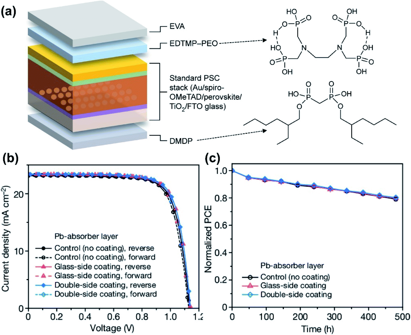 | ||
| Fig. 12 (a) PPV device architecture with front and back Pb-absorbing coating layers. Comparison of the J–V curves (b) and operation stability (c) for PPVs with and without the Pb-absorbing layers. Reproduced from ref. 112 with permission from Springer Nature. | ||
3.4 Others
Compared with outdoor light, common indoor light sources not only have different spectrum and irradiance intensities but also contain both oblique direct light and isotropic diffuse light,115 which have been rarely considered in current PV studies and may impose a challenge in the standardisation of indoor testing of PV devices. Rational materials and device design of PV devices to achieve a broad angular response may be extremely beneficial to maximise device performance under low light conditions. In addition, partial shading on the device surface is more likely to occur in a complex indoor environment, which may introduce inadvertent reverse bias to individual devices and lead to device degradation similar to that under outdoor light.116 Development of PV devices robust to reverse bias conditions may be a further important consideration to achieve long term stability under low light. It should also be noted that indoor PVs and outdoor PVs can have very different requirements for solar cell stability and lifetimes owing to their different target applications. For example, compared to outdoor applications (e.g. power plants, building-integrated PV applications) that typically require a PV device lifetime of more than 25 years, indoor PV applications may require a much shorter PV device lifetime (e.g. integration with consumer electronics or wireless sensors, which have a typical lifespan of less than 3–5 years), suggesting that solution-processed solar cells have tremendous commercialisation potential for indoor applications and may achieve commercialisation ahead of outdoor PVs. Finally, ensuring a low production cost to adapt the market requirement (such as low price sensors) is necessary in order to maximise the commercialisation potential of solution-processed solar cells as a competitive PV technology for low light applications.4 Summary
In this review, we have summarised the latest research progress on the development of solution-processed organic, perovskite and quantum dot semiconductors and devices targeting indoor PV applications. With outstanding device performance and lifetimes already achieved to date, these emerging PV technologies have demonstrated tremendous potential toward developing into a commercially viable product for use in a broad range of indoor PV applications. It is expected that further rapid enhancements are achievable both in their efficiency and stability in the near future, considering that a theoretical maximum efficiency of up to 52% has been predicted for PV devices under 1000 lx cool white LEDs with a bandgap ∼1.9 eV.48However, several substantial challenges still remain toward the commercialisation of this emerging PV technology, in particular associated with their limited stability and ecotoxicity. Overcoming these challenges requires substantial further research efforts. However, with the rapid advances in the materials and devices of these emerging PV technologies, it is envisaged that they will realise their full potential for commercialisation in the near future.
Author contributions
XH and YW contributed equally to this work and were in charge of writing the manuscript. HL and RD contributed to writing the Standards of PV characterisation part. NM and DY contributed to part of the perovskite and quantum dot literature summary. HL, WT, ML, FZ, BH and ZL revised the content.Conflicts of interest
There are no conflicts to declare.Acknowledgements
XH, YW and ZL acknowledge the funding from the Engineering and Physical Sciences Research Council (EP/S020748/1). BH would like to acknowledge the financial support from Cardiff University. HL, RD and WT would like to thank Airbus Endeavr Wales for the financial support and the SPECIFIC Innovation and Knowledge Centre (EP/N020863/1) for funding.References
- H. K. H. Lee, J. Barbé and W. C. Tsoi, Solar Cells and Light Management, 2020, pp. 355–388 Search PubMed.
- A. Venkateswararao, J. K. Ho, S. K. So, S.-W. Liu and K.-T. Wong, Mater. Sci. Eng., R, 2019, 139, 100517 CrossRef.
- M. Otsuka, Y. Kurokawa, Y. Ding, F. B. Juangsa, S. Shibata, T. Kato and T. Nozaki, RSC Adv., 2020, 10, 12611–12618 RSC.
- P. K. B. R. E. Hollingsworth and A. Madan, J. Non-Cryst. Solids, 1987, 97–98, 309–312 CrossRef.
- M. K. K Fukutani, W. Futako, B. Kaplan, T. Kamiya, C. M Fortmann and I. Shimizu, J. Non-Cryst. Solids, 1998, 227–230, 63–67 CrossRef.
- Y. Dai, H. Kum, M. A. Slocum, G. T. Nelson and S. M. Hubbard, IEEE 44th Photovoltaic Specialist Conference, PVSC, 2017, pp. 222–225 Search PubMed.
- N. Espinosa, M. Hösel, D. Angmo and F. C. Krebs, Energy Environ. Sci., 2012, 5, 5117–5132 RSC.
- S. C. L. K. T. Ibn-Mohammed, I. M. Reaney, A. Acquaye, G. Schileo, K. B. Mustapha and R. Greenough, Renewable Sustainable Energy Rev., 2017, 80, 1321–1344 CrossRef.
- L.-K. Ma, Y. Chen, P. C. Chow, G. Zhang, J. Huang, C. Ma, J. Zhang, H. Yin, A. M. H. Cheung and K. S. Wong, Joule, 2020, 4, 1486–1500 CrossRef CAS.
- Y. W. Noh, I. S. Jin, K. S. Kim, S. H. Park and J. W. Jung, J. Mater. Chem. A, 2020, 8, 17163–17173 RSC.
- B. Hou, B.-S. Kim, H. K. H. Lee, Y. Cho, P. Giraud, M. Liu, J. Zhang, M. L. Davies, J. R. Durrant, W. C. Tsoi, Z. Li, S. D. Dimitrov, J. I. Sohn, S. Cha and J. M. Kim, Adv. Funct. Mater., 2020, 2004563 CrossRef CAS.
- I. Mathews, S. N. Kantareddy, T. Buonassisi and I. M. Peters, Joule, 2019, 3, 1415–1426 CrossRef CAS.
- J. Kalowekamo and E. Baker, Sol. Energy, 2009, 83, 1224–1231 CrossRef CAS.
- Z. Song, C. L. McElvany, A. B. Phillips, I. Celik, P. W. Krantz, S. C. Watthage, G. K. Liyanage, D. Apul and M. J. Heben, Energy Environ. Sci., 2017, 10, 1297–1305 RSC.
- D. C. Bobela, L. Gedvilas, M. Woodhouse, K. A. W. Horowitz and P. A. Basore, Prog. Photovoltaics, 2017, 25, 41–48 Search PubMed.
- Y. Cui, H. Yao, J. Zhang, K. Xian, T. Zhang, L. Hong, Y. Wang, Y. Xu, K. Ma and C. An, Adv. Mater., 2020, 32, 1908205 CrossRef CAS.
- Y. Cui, Y. Wang, J. Bergqvist, H. Yao, Y. Xu, B. Gao, C. Yang, S. Zhang, O. Inganäs and F. Gao, Nat. Energy, 2019, 4, 768–775 CrossRef CAS.
- R. Steim, T. Ameri, P. Schilinsky, C. Waldauf, G. Dennler, M. Scharber and C. J. Brabec, Sol. Energy Mater. Sol. Cells, 2011, 95, 3256–3261 CrossRef CAS.
- B. P. Lechêne, M. Cowell, A. Pierre, J. W. Evans, P. K. Wright and A. C. Arias, Nano Energy, 2016, 26, 631–640 CrossRef.
- S. R. Cowan, A. Roy and A. J. Heeger, Phys. Rev. B: Condens. Matter Mater. Phys., 2010, 82, 245207 CrossRef.
- L. J. A. Koster, V. D. Mihailetchi, R. Ramaker and P. W. Blom, Appl. Phys. Lett., 2005, 86, 123509 CrossRef.
- Y. Wang, B. Wu, Z. Wu, Z. Lan, Y. Li, M. Zhang and F. Zhu, J. Phys. Chem. Lett., 2017, 8, 5264–5271 CrossRef CAS.
- H. K. Lee, Z. Li, J. R. Durrant and W. C. Tsoi, Appl. Phys. Lett., 2016, 108, 253301 CrossRef.
- S. Mori, T. Gotanda, Y. Nakano, M. Saito, K. Todori and M. Hosoya, Jpn. J. Appl. Phys., 2015, 54, 071602 CrossRef.
- B. Xiao, P. Calado, R. C. I. MacKenzie, T. Kirchartz, J. Yan and J. Nelson, Phys. Rev. Appl., 2020, 14, 024034 CrossRef CAS.
- S. S. Yang, Z. C. Hsieh, M. L. Keshtov, G. D. Sharma and F. C. Chen, Sol. RRL, 2017, 1, 1700174 CrossRef.
- Y. J. You, C. E. Song, Q. V. Hoang, Y. Kang, J. S. Goo, D. H. Ko, J. J. Lee, W. S. Shin and J. W. Shim, Adv. Funct. Mater., 2019, 29, 1901171 CrossRef.
- Y. Cui, H. Yao, T. Zhang, L. Hong, B. Gao, K. Xian, J. Qin and J. Hou, Adv. Mater., 2019, 31, 1904512 CrossRef CAS.
- M. Freunek, M. Freunek and L. M. Reindl, IEEE Journal of Photovoltaics, 2012, 3, 59–64 Search PubMed.
- Z. Ding, R. Zhao, Y. Yu and J. Liu, J. Mater. Chem. A, 2019, 7, 26533–26539 RSC.
- H. K. H. Lee, J. Wu, J. Barbé, S. M. Jain, S. Wood, E. M. Speller, Z. Li, F. A. Castro, J. R. Durrant and W. C. Tsoi, J. Mater. Chem. A, 2018, 6, 5618–5626 RSC.
- R. Singh, S.-C. Shin, H. Lee, J. W. Shim, K. Cho and J.-J. Lee, Chem.–Eur. J., 2019, 25, 6154–6161 CrossRef CAS.
- H. Yin, J. K. W. Ho, S. H. Cheung, R. J. Yan, K. L. Chiu, X. Hao and S. K. So, J. Mater. Chem. A, 2018, 6, 8579–8585 RSC.
- Y. Cho, T. Kumari, S. Jeong, S. M. Lee, M. Jeong, B. Lee, J. Oh, Y. Zhang, B. Huang and L. Chen, Nano Energy, 2020, 75, 104896 CrossRef CAS.
- M. Nam, H. Y. Noh, J. Cho, Y. Park, S. C. Shin, J. A. Kim, J. Kim, H. H. Lee, J. W. Shim and D. H. Ko, Adv. Funct. Mater., 2019, 29, 1900154 CrossRef.
- H. Yin, S. Chen, S. H. Cheung, H. W. Li, Y. Xie, S. W. Tsang, X. Zhu and S. K. So, J. Mater. Chem. C, 2018, 6, 9111–9118 RSC.
- S.-C. Shin, C. W. Koh, P. Vincent, J. S. Goo, J.-H. Bae, J.-J. Lee, C. Shin, H. Kim, H. Y. Woo and J. W. Shim, Nano Energy, 2019, 58, 466–475 CrossRef CAS.
- R. Arai, S. Furukawa, Y. Hidaka, H. Komiyama and T. Yasuda, ACS Appl. Mater. Interfaces, 2019, 11, 9259–9264 CrossRef CAS.
- R. Arai, S. Furukawa, N. Sato and T. Yasuda, J. Mater. Chem. A, 2019, 7, 20187–20192 RSC.
- V. V. Brus, J. Lee, B. R. Luginbuhl, S. J. Ko, G. C. Bazan and T. Q. Nguyen, Adv. Mater., 2019, 31, 1900904 CrossRef.
- H. Yin, J. K. W. Ho, V. Piradi, S. Chen, X. Zhu and S. K. So, Small Methods, 2020, 4, 2000136 CrossRef.
- B. R. Lee, J. S. Goo, Y. W. Kim, Y.-J. You, H. Kim, S.-K. Lee, J. W. Shim and T. G. Kim, J. Power Sources, 2019, 417, 61–69 CrossRef CAS.
- NationalRenewableEnergyLaboratory, Best Research-Cell Efficiency, 2020 Search PubMed.
- K. X. Steirer, P. Schulz, G. Teeter, V. Stevanovic, M. Yang, K. Zhu and J. J. Berry, ACS Energy Lett., 2016, 1, 360–366 CrossRef CAS.
- C. Y. Chen, J. H. Chang, K. M. Chiang, H. L. Lin, S. Y. Hsiao and H. W. Lin, Adv. Funct. Mater., 2015, 25, 7064–7070 CrossRef CAS.
- P.-K. Kung, M.-H. Li, P.-Y. Lin, J.-Y. Jhang, M. Pantaler, D. C. Lupascu, G. Grancini and P. Chen, Sol. RRL, 2020, 4, 1900306 CrossRef CAS.
- S. P. Dunfield, L. Bliss, F. Zhang, J. M. Luther, K. Zhu, M. F. van Hest, M. O. Reese and J. J. Berry, Adv. Energy Mater., 2020, 10, 1904054 CrossRef CAS.
- G. Jarosz, R. Marczyński and R. Signerski, Mater. Sci. Semicond. Process., 2020, 107, 104812 CrossRef.
- Q. Fu, X. Tang, B. Huang, T. Hu, L. Tan, L. Chen and Y. Chen, Adv. Sci.c, 2018, 5, 1700387 CrossRef.
- Q. Wang, N. Phung, D. Di Girolamo, P. Vivo and A. Abate, Energy Environ. Sci., 2019, 12, 865–886 RSC.
- R. Cheng, C. C. Chung, H. Zhang, F. Liu, W. T. Wang, Z. Zhou, S. Wang, A. B. Djurišić and S. P. Feng, Adv. Energy Mater., 2019, 9, 1901980 CrossRef CAS.
- J. W. Lim, H. Kwon, S. H. Kim, Y.-J. You, J. S. Goo, D.-H. Ko, H. J. Lee, D. Kim, I. Chung, T. G. Kim, D. H. Kim and J. W. Shim, Nano Energy, 2020, 75, 104984 CrossRef CAS.
- M. H. Ann, J. Kim, M. Kim, G. Alosaimi, D. Kim, N. Y. Ha, J. Seidel, N. Park, J. S. Yun and J. H. Kim, Nano Energy, 2020, 68, 104321 CrossRef CAS.
- S. Yang, H. Zhao, Y. Han, C. Duan, Z. Liu and S. Liu, Small, 2019, 15, 1904387 CrossRef CAS.
- J. Dagar, S. Castro-Hermosa, G. Lucarelli, F. Cacialli and T. M. Brown, Nano Energy, 2018, 49, 290–299 CrossRef CAS.
- H. K. H. Lee, J. Barbé, S. M. Meroni, T. Du, C. T. Lin, A. Pockett, J. Troughton, S. M. Jain, F. De Rossi and J. Baker, Sol. RRL, 2019, 3, 1800207 CrossRef.
- M. Li, C. Zhao, Z. K. Wang, C. C. Zhang, H. K. Lee, A. Pockett, J. Barbé, W. C. Tsoi, Y. G. Yang and M. J. Carnie, Adv. Energy Mater., 2018, 8, 1801509 CrossRef.
- F. Di Giacomo, V. Zardetto, G. Lucarelli, L. Cinà, A. Di Carlo, M. Creatore and T. Brown, Nano Energy, 2016, 30, 460–469 CrossRef CAS.
- J. Feng, X. Zhu, Z. Yang, X. Zhang, J. Niu, Z. Wang, S. Zuo, S. Priya, S. Liu and D. Yang, Adv. Mater., 2018, 30, 1801418 CrossRef.
- B. Cao, L. Yang, S. Jiang, H. Lin, N. Wang and X. Li, J. Mater. Chem. A, 2019, 7, 4960–4970 RSC.
- F. Di Giacomo, A. Fakharuddin, R. Jose and T. M. Brown, Energy Environ. Sci., 2016, 9, 3007–3035 RSC.
- H. Xie, X. Yin, Y. Guo, J. Liu, W. Que and G. Wang, Phys. Status Solidi RRL, 2019, 13, 1800566 CrossRef.
- G. Lucarelli, F. Di Giacomo, V. Zardetto, M. Creatore and T. M. Brown, Nano Res., 2017, 10, 2130–2145 CrossRef CAS.
- J. Dagar, S. Castro-Hermosa, M. Gasbarri, A. L. Palma, L. Cina, F. Matteocci, E. Calabrò, A. Di Carlo and T. M. Brown, Nano Res., 2018, 11, 2669–2681 CrossRef CAS.
- A. H. Ali, Z. Hassan and A. Shuhaimi, Appl. Surf. Sci., 2018, 443, 544–547 CrossRef CAS.
- S. Castro-Hermosa, G. Lucarelli, M. Top, M. Fahland, J. Fahlteich and T. M. Brown, Cell Reports Physical Science, 2020, 1, 100045 CrossRef.
- S. Kim, H. Oh, G. Kang, I. K. Han, I. Jeong and M. Park, ACS Appl. Energy Mater., 2020, 3, 6995–7003 CrossRef CAS.
- Z. Li, T. R. Klein, D. H. Kim, M. Yang, J. J. Berry, M. F. van Hest and K. Zhu, Nat. Rev. Mater., 2018, 3, 1–20 CrossRef CAS.
- N.-G. Park and K. Zhu, Nat. Rev. Mater., 2020, 5, 333–350 CrossRef CAS.
- J. E. Bishop, C. D. Read, J. A. Smith, T. J. Routledge and D. G. Lidzey, Scientific reports, 2020, 10, 1–8 CrossRef.
- T. Bu, X. Liu, J. Li, W. Huang, Z. Wu, F. Huang, Y.-B. Cheng and J. Zhong, Sol. RRL, 2020, 4, 1900263 CrossRef CAS.
- F. De Rossi, J. A. Baker, D. Beynon, K. E. A. Hooper, S. M. P. Meroni, D. Williams, Z. Wei, A. Yasin, C. Charbonneau, E. H. Jewell and T. M. Watson, Adv. Mater. Technol., 2018, 3, 1800156 CrossRef.
- B. Hou, Isr. J. Chem., 2019, 59, 637–638 CrossRef CAS.
- B. Li, M. Lu, J. Feng, J. Zhang, P. M. Smowton, J. I. Sohn, I.-K. Park, H. Zhong and B. Hou, J. Mater. Chem. C, 2020, 8, 10676–10695 RSC.
- C.-H. M. Chuang, P. R. Brown, V. Bulović and M. G. Bawendi, Nat. Mater., 2014, 13, 796–801 CrossRef CAS.
- Z. Ning, O. Voznyy, J. Pan, S. Hoogland, V. Adinolfi, J. Xu, M. Li, A. R. Kirmani, J.-P. Sun and J. Minor, Nat. Mater., 2014, 13, 822–828 CrossRef CAS.
- M. C. Beard, J. M. Luther, O. E. Semonin and A. J. Nozik, Acc. Chem. Res., 2013, 46, 1252–1260 CrossRef CAS.
- M. C. Beard, A. G. Midgett, M. C. Hanna, J. M. Luther, B. K. Hughes and A. J. Nozik, Nano Lett., 2010, 10, 3019–3027 CrossRef CAS.
- A. J. Nozik, Annu. Rev. Phys. Chem., 2001, 52, 193–231 CrossRef CAS.
- A. Shabaev, A. L. Efros and A. Nozik, Nano Lett., 2006, 6, 2856–2863 CrossRef CAS.
- Y. Bi, S. Pradhan, S. Gupta, M. Z. Akgul, A. Stavrinadis and G. Konstantatos, Adv. Mater., 2018, 30, 1704928 CrossRef.
- B. Sun, A. Johnston, C. Xu, M. Wei, Z. Huang, Z. Jiang, H. Zhou, Y. Gao, Y. Dong, O. Ouellette, X. Zheng, j. Liu, M.-J. Choi, Y. Gao, S.-W. Baek, F. Laquai, O. M. Bakr, D. Ban, O. Voznyy, F. P. Garcia de Arquer and E. H. Sargent, Joule, 2020, 4, 1542–1556 CrossRef CAS.
- M.-J. Choi, F. P. G. de Arquer, A. H. Proppe, A. Seifitokaldani, J. Choi, J. Kim, S.-W. Baek, M. Liu, B. Sun and M. Biondi, Nat. Commun., 2020, 11, 1–9 Search PubMed.
- B. Hou, Y. Cho, B. S. Kim, J. Hong, J. B. Park, S. J. Ahn, J. I. Sohn, S. Cha and J. M. Kim, ACS Energy Lett., 2016, 1, 834–839 CrossRef CAS.
- B. Hou, Y. Cho, B.-S. Kim, D. Ahn, S. Lee, J. B. Park, Y.-W. Lee, J. Hong, H. Im and S. M. Morris, J. Mater. Chem. C, 2017, 5, 3692–3698 RSC.
- A. Kiani, H. Fayaz Movahed, S. Hoogland, O. Voznyy, R. Wolowiec, L. Levina, F. P. Garcia de Arquer, P. Pietsch, X. Wang, P. Maraghechi and E. H. Sargent, ACS Energy Lett., 2016, 1, 740–746 CrossRef CAS.
- J. K. W. Ho, H. Yin and S. K. So, J. Mater. Chem. A, 2020, 8, 1717–1723 RSC.
- B. Minnaert and P. Veelaert, Energies, 2014, 7, 1500–1516 CrossRef.
- M. Mainville and M. Leclerc, ACS Energy Lett., 2020, 5, 1186–1197 CrossRef CAS.
- B. H. Hamadani and M. B. Campanelli, IEEE Journal of Photovoltaics, 2020, 10, 1119–1125 Search PubMed.
- C.-Y. Chen, Z.-H. Jian, S.-H. Huang, K.-M. Lee, M.-H. Kao, C.-H. Shen, J.-M. Shieh, C.-L. Wang, C.-W. Chang and B.-Z. Lin, J. Phys. Chem. Lett., 2017, 8, 1824–1830 CrossRef CAS.
- Z. Li, E. Speller, J. Durrant, J.-S. Kim, W. Tsoi, A. J. Clarke, J. Luke, T. Wang, H. C. Wong and H. Lee, J. Mater. Chem. A, 2019, 7, 23361–23377 RSC.
- Y. Wang, W. Lan, N. Li, Z. Lan, Z. Li, J. Jia and F. Zhu, Adv. Energy Mater., 2019, 9, 1900157 CrossRef.
- E. M. Speller, A. J. Clarke, N. Aristidou, M. F. Wyatt, L. Francàs, G. Fish, H. Cha, H. K. H. Lee, J. Luke and A. Wadsworth, ACS Energy Lett., 2019, 4, 846–852 CrossRef CAS.
- Z. Li, J. Nelson, H. Lee, J. Durrant, J. A. Röhr, A. Telford, M. F. Wyatt, B. Rice, J. Wu and J. McGettrick, Energy Environ. Sci., 2018, 11, 417–428 RSC.
- E. M. Speller, J. D. McGettrick, B. Rice, A. M. Telford, H. K. Lee, C.-H. Tan, C. S. De Castro, M. L. Davies, T. M. Watson and J. Nelson, ACS Appl. Mater. Interfaces, 2017, 9, 22739–22747 CrossRef CAS.
- N. Li, J. D. Perea, T. Kassar, M. Richter, T. Heumueller, G. J. Matt, Y. Hou, N. S. Güldal, H. Chen and S. Chen, Nat. Commun., 2017, 8, 14541 CrossRef CAS.
- T. S. Glen, N. W. Scarratt, H. Yi, A. Iraqi, T. Wang, J. Kingsley, A. R. Buckley, D. G. Lidzey and A. M. Donald, J. Polym. Sci., Part B: Polym. Phys., 2016, 54, 216–224 CrossRef CAS.
- H. Jin, E. Debroye, M. Keshavarz, I. G. Scheblykin, M. B. Roeffaers, J. Hofkens and J. A. Steele, Mater. Horiz., 2020, 7, 397–410 RSC.
- R. Chen, Y. Hui, B. Wu, Y. Wang, X. Huang, Z. Xu, P. Ruan, W. Zhang, F. Cheng and W. Zhang, J. Mater. Chem. A, 2020, 8, 9597–9606 RSC.
- T. Singh and T. Miyasaka, Adv. Energy Mater., 2018, 8, 1700677 CrossRef.
- C. Li, J. Yin, R. Chen, X. Lv, X. Feng, Y. Wu and J. Cao, J. Am. Chem. Soc., 2019, 141, 6345–6351 CrossRef CAS.
- N. D. Pham, J. Shang, Y. Yang, M. T. Hoang, V. T. Tiong, X. Wang, L. Fan, P. Chen, L. Kou and L. Wang, Nano Energy, 2020, 69, 104412 CrossRef CAS.
- H. D. Pham, S. M. Jain, M. Li, Z. K. Wang, S. Manzhos, K. Feron, S. Pitchaimuthu, Z. Liu, N. Motta and J. R. Durrant, Adv. Electron. Mater., 2020, 6, 1900884 CrossRef CAS.
- L. K. Jagadamma, O. Blaszczyk, M. T. Sajjad, A. Ruseckas and I. D. Samuel, Sol. Energy Mater. Sol. Cells, 2019, 201, 110071 CrossRef CAS.
- S. Sidhik, C. R. Pérez, M. A. S. Estrada, T. López-Luke, A. Torres and E. De la Rosa, Sol. Energy, 2020, 202, 438–445 CrossRef CAS.
- M. Hadadian, J.-H. Smått and J.-P. Correa-Baena, Energy Environ. Sci., 2020, 13, 1377–1407 RSC.
- H.-I. Je, E.-Y. Shin, K. J. Lee, H. Ahn, S. Park, S. H. Im, Y.-H. Kim, H. J. Son and S.-K. Kwon, ACS Appl. Mater. Interfaces, 2020, 12, 23181–23189 CrossRef CAS.
- J. Li, H.-L. Cao, W.-B. Jiao, Q. Wang, M. Wei, I. Cantone, J. Lü and A. Abate, Nat. Commun., 2020, 11, 1–5 CAS.
- M. Bernechea, N. C. Miller, G. Xercavins, D. So, A. Stavrinadis and G. Konstantatos, Nat. Photonics, 2016, 10, 521–525 CrossRef CAS.
- T. Miyasaka, A. Kulkarni, G. M. Kim, S. Öz and A. K. Jena, Adv. Energy Mater., 2020, 10, 1902500 CrossRef CAS.
- X. Li, F. Zhang, H. He, J. J. Berry, K. Zhu and T. Xu, Nature, 2020, 578, 555–558 CrossRef CAS.
- J. Wang, F. Di Giacomo, J. Brüls, H. Gorter, I. Katsouras, P. Groen, R. A. Janssen, R. Andriessen and Y. Galagan, Sol. RRL, 2017, 1, 1700091 CrossRef.
- X. Cao, G. Zhang, L. Jiang, Y. Cai, Y. Gao, W. Yang, X. He, Q. Zeng, G. Xing and Y. Jia, ACS Appl. Mater. Interfaces, 2019, 12, 5825–5931 Search PubMed.
- C. A. Reynaud, R. Clerc, P. B. Lechêne, M. Hébert, A. Cazier and A. C. Arias, Sol. Energy Mater. Sol. Cells, 2019, 200, 110010 CrossRef CAS.
- R. A. Razera, D. A. Jacobs, F. Fu, P. Fiala, M. Dussouillez, F. Sahli, T. C. Yang, L. Ding, A. Walter and A. F. Feil, J. Mater. Chem. A, 2020, 8, 242–250 RSC.
Footnote |
| † These authors contribute equally. |
| This journal is © The Royal Society of Chemistry 2020 |