
 Open Access Article
 This Open Access Article is licensed under a Creative Commons Attribution-Non Commercial 3.0 Unported Licence
The fox and the hound: in-depth and in-grain Na doping and Ga grading in Cu(In,Ga)Se2 solar cells†
Diego
Colombara
 *ab,
Kevin
Conley
c,
Maria
Malitckaya
c,
Hannu-Pekka
Komsa
*cd and
Martti J.
Puska
c
*ab,
Kevin
Conley
c,
Maria
Malitckaya
c,
Hannu-Pekka
Komsa
*cd and
Martti J.
Puska
c
aUniversità degli Studi di Genova, via Dodecaneso 31, 16146 Genova, Italy. E-mail: diego.colombara@bath.edu
bInternational Iberian Nanotechnology Laboratory, av. Mestre José Veiga, 4715-330 Braga, Portugal
cDepartment of Applied Physics, Aalto University, P. O. Box 11000, 00076 Aalto, Finland. E-mail: hannu-pekka.komsa@oulu.fi
dMicroelectronics Research Unit, Faculty of Information Technology and Electrical Engineering, University of Oulu, P.O. Box 8000, 90014, Finland
First published on 30th March 2020
Abstract
Cu(In,Ga)(S,Se)2 (CIGS) thin film solar cells require appropriate depth and lateral distributions of alkali metal dopants and gallium to attain world record photovoltaic energy conversion. The two requirements are interdependent because sodium is known to hamper In/Ga interdiffusion in polycrystalline films. However, such a fact is challenged by recent findings where sodium appears to enhance In/Ga interdiffusion in monocrystalline films. This contribution reviews closely the two cases to the benefits of grain boundary engineering in CIGS. A computational model reveals why Na induces In accumulation at CIGS grain boundaries, confining Ga to grain interiors. The positive technological implications for wider gap chalcopyrites are stressed.
Introduction
Solar power is central to the sustainable growth of humankind. With 23.35% efficiency, Cu(In,Ga)(S,Se)2 (CIGS) solar cells display the highest ever reported light to electricity conversion of all commercially available thin film photovoltaic technologies.2 Excitingly, there is still room for improvement at both cell and module levels.3Thanks to the possibility to alloy CuInSe2 (CIS) and CuGaSe2 (CGS), the CIGS band-gap can be tuned from ca. 1.0 eV (CIS) to ca. 1.7 eV (CGS), allowing for both single and double junction device fabrication.4
Commercial CIGS solar cells are currently based on a highly engineered single junction configuration that is the result of cumulative knowledge gathered during 30+ years of R&D. Fig. 1 shows the historical progress of record power conversion efficiency for laboratory CIGS cells since the inception.5 Throughout this (sometimes serendipitous) journey three strategies have played a crucial role for technological success:
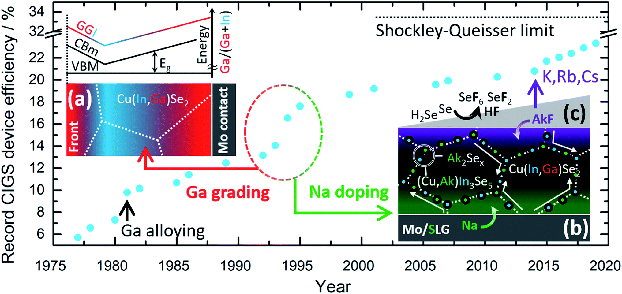 | ||
| Fig. 1 Historical progress of CIGS solar cell efficiency at laboratory scale with emphasis on the major technological breakthroughs, shown as schematic insets with illustrative purposes: (a) Ga grading, (b) Na doping and (c) the more recent doping by heavier alkali metal post deposition treatments (PDT). Acronyms are as follows; GGI: atomic concentration ratio of Ga over the sum of Ga and In, VBM: valence band maximum, CBm: conduction band minimum, Eg: band-gap energy, AkF: generic alkali metal fluoride, SLG: soda-lime glass. | ||
(a) The controlled gradient of Ga concentration relative to In through the depth of the film,6Fig. 1a.
(b) The deliberate doping with Na,7Fig. 1b.
(c) The post deposition treatment (PDT) with heavier alkali metal fluorides (KF,8–10 RbF and CsF11), Fig. 1c.
Soon after Na was found to be beneficial for cell efficiency, it was also shown to impede the interdiffusion of In and Ga. Later, K was also observed to hinder In/Ga interdiffusion.12 This effect has been exploited to tailor specifically the Ga grading in films produced by reactive annealing of sputtered metallic precursors.13 Therefore, the two above strategies are closely entangled, although they have been historically pursued in parallel without attempting to purposely engineer one another.
The beneficial effect of heavy alkali PDT was first connected to the changes in the absorber surface chemistry and morphology.14,15 A phase containing K–In–Se with a wider band gap was observed which was connected to the reduced absorber–buffer interface recombination and increased open-circuit voltage.15,16 Moreover, the improved surface morphology enables a thinner buffer layer resulting in reduced optical losses.14 Most recently, based on the observation of similar open-circuit voltage improvements, instead of different surface conditions it was concluded that the improvements in the bulk absorber play the most important role.17 Namely, heavy alkali metal atoms can diffuse along grain boundaries accumulating on them and also substitute the proximate Na atoms.14,16 This leads to the passivation of charged defects at the grain boundaries which reduces the concentration of tail states inside the grains. The result is reduced recombination and increased open-circuit voltage.17
This contribution focuses on the influence of Na and K on the interdiffusion of In and Ga. Generally, it is well known that grain boundaries in polycrystalline materials have a strong influence on mass transport properties18 and the same is true for Na along CIGS grain boundaries.19 Therefore, it is important to understand if the hindering effect of Na and K on the interdiffusion of In and Ga in CIGS is related to transport at the grain boundaries or is intrinsically related to bulk CIGS properties.
In such cases, a constructionist approach can reduce the complex interdependency between variables, rendering the system more manageable, as demonstrated for macroscopic20 and mesoscopic21 crystals.
Through a parallel approach, a recent study has shown that Na can enhance the interdiffusion of In and Ga in monocrystalline CIGS films, contrary to the polycrystalline case.1 Precisely, Na appears to either enhance or impede the diffusion of In and Ga depending on the relative concentration of Na and Cu.22 This paper reviews Na doping and Ga grading in CIGS with a comparison between the historical and recently discovered interdependences.
Learning from CIGS′ past breakthroughs
The fox: sodium doping
Today's CIGS technology relies on Na as an essential extrinsic dopant to ensure the best optoelectronic properties.8,23,24 The first encounter between Na and CIGS dates to 1993, when Hedström et al. observed that CIGS grown on soda-lime glass substrates yielded cells with substantially higher open circuit voltage and fill factor compared to CIGS grown on Na-free substrates.7 It was later established by Granata et al. that the Na concentration for optimum performance ranges between 0.05 at% and 0.5 at%.25The device's improvement induced by Na doping is attributed to increased p-type conductivity and defect passivation,26 but the detailed underlying mechanism is still debated. It has been suggested that Na catalyzes the oxygenation of Se vacancies,27 forms Na(In,Ga) acceptors,28 eliminates (In,Ga)Cu donors29 or increases the concentration of Cu vacancies (VCu) due to differential solubility of NaCu during CIGS growth and cool down.30 All these proposed mechanisms have strengths and weaknesses, but none of them can be claimed to unify all the experimental evidence and stand against theoretical scrutiny.
Indeed, the effects of Na doping in CIGS are not limited to electronic properties. Besides impeding atomic diffusion,7,12,31–39 Na also affects grain growth and texture.7,32,40–44
These unexplained “symptoms” remain rather understudied, but, conceivably, represent the other side of the coin.45 Studying them may add one crucial link to understand CIGS from the material viewpoint and help unlock the full potential of the technology towards the Shockley–Queisser limit.
The hound: gallium grading
Thanks to the nearly invariant CIS and CGS valence band levels, typical v-shaped gradients of Ga/(Ga + In) (GGI) through the depth of CIGS films correspond to a v-shaped conduction band level. Such a configuration has been beneficial because it acts as a back surface field, and is thought to ease the collection of photogenerated electrons while reducing interface recombination39,46 (Fig. 1a).GGI depth gradients were first deliberately engineered at NREL by Contreras et al. in 1993 with the introduction of the 3-stage co-evaporation process.6,47–49 However, it soon became apparent that (steep) gradients tend to form spontaneously also during sequential processing (chalcogenization of metal precursor films) if Na is present during the growth.50–52 As such, the phenomenon concerns the two major industrial routes of commercial CIGS modules.
Simulations by Witte et al.39 show that cell efficiency depends critically on the exact position of the notch point, with a trade-off between open circuit voltage and short circuit current. In fact though, the minority carrier diffusion length in modern devices is sufficient to ensure good current collection without the need for v-shaped gradients.53 Hence, the community will soon have to adjust the film growth conditions to allow for a modified outcome of In/Ga interdiffusion.
Besides the deliberate depth grading, accidental GGI gradients can also occur laterally, leading to so-called band-gap fluctuations.54 These inhomogeneities are a source of voltage losses in record cells below 20% efficiency.55,56
When going from lab-scale to large industrial areas the range of fluctuations increases from sub-micrometer to micrometer length scale. This is because absolute control of In and Ga lateral concentration in CIGS modules can be problematic.3,57 Such fluctuations can contribute to performance losses beyond the effect of parallel electrical connection,58 as the module's minority carrier diffusion length is progressively increased.56
The elusive friendship between the fox and the hound
The hindering effect of Na on In/Ga interdiffusion in polycrystalline CIGS films is supported by evidence gathered over 20 years by independent research groups using different experimental approaches.12,31–33,35–39,50,59 If Na is present during the growth, its actual source does not appear to be very important. Decreased In/Ga interdiffusion was observed regardless of the Cu/III ratio33,38 and of the Na origin such as: NaF pre-deposited on either Mo-coated soda-lime glass (SLG)/Al2O3 (ref. 31) or polyimide foils,36 or supplied during the growth31,37 or during the selenization59 or resulting from diffusion respectively out of soda-lime glass31–33,38,50 or enamel coated steel substrates,12 when the films are compared to respective “Na-free” reference samples. Retrospectively, this is consistent with the high Na mobility in the CIGS lattice revealed both by theory and experiment.19,60 In other words, Na will diffuse and yield similar effects over its large diffusion length scale, regardless of the source location (front/back), if present during the growth.However, larger-scale inhomogeneous distributions of alkali dopants during film growth may still translate into undesired GGI distributions in the final device, given the influence of the dopants on In/Ga diffusion. Since these fluctuations are detrimental to performance, controlling the uniformity of sodium and potassium doping is crucial.26,61,62
Understanding the interdependence between alkali metal doping and GGI gradients would then allow to take better control over the intermixing behaviour of In and Ga in CIGS (both laterally and in-depth) with positive repercussions on the technology. A deeper diffusion mechanistic knowledge will also prove useful when tackling changes in cell geometry from the conventional configuration towards thinner63 and micropattern64,65 CIGS devices.
Rodriguez-Alvarez38 and Witte et al.39 offer an exhaustive account of the interdependence between Na doping and Ga grading in polycrystalline CIGS. Their studies reveal a clear relationship between Na and Cu, confirming that:
(a) Diffusion of In and Ga occurs through the Cu sublattice, as previously suggested by Schroeder et al.66 (Fig. 2a);
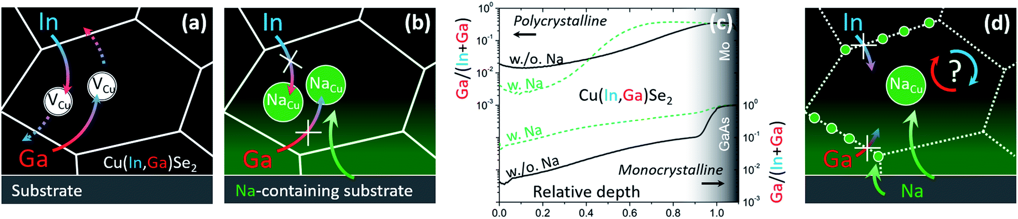 | ||
| Fig. 2 (a) Schematics of In/Ga interdiffusion mediated by Cu vacancies in Na-free CIGS and (b) impeded interdiffusion according to the commonly accepted rationale. (c) Ga/(In + Ga) secondary ion mass spectrometry depth profiles of Na-free (solid black) and Na-containing (dashed green) polycrystalline (top)59 and monocrystalline (bottom)1 CIGS films. (d) Phenomenological interpretation following the findings in monocrystalline CIGS.1 | ||
(b) Na is likely to interfere with Cu vacancies, as inferred by Lundberg et al.33 (Fig. 2b).
It is then commonly agreed that the hindering effect of Na at high temperature should be ascribed to a decreased concentration of Cu vacancies resulting from the capture of Na and formation of NaCu substitutional defects,30 as originally proposed by Rudmann et al.32 An analogous argument was recently proposed by Cai et al. for potassium, with the formation of KCu substitutionals.13
In and Ga atoms occupy the same CIGS lattice sites and thus diffuse interdependently. Repins et al. were able to simulate GGI depth profiles in CIGS films obtained by the 3-stage process through a modification of the diffusion equations taking into account In/Ga atomic site sharing.67 However, engineering GGI gradients by means of tuning the Na or K concentration gradients in the films requires knowledge of the migration paths also via the grain boundaries.
In fact, the accepted paradigm is challenged by newer findings on monocrystalline CIGS films.1 These show that diffusion of Ga from GaAs substrates into epitaxial CIS films (i.e. free from high-angle grain boundaries) is substantially enhanced by the presence of Na (introduced even from the front surface, Fig. 2c). Given that these findings seemingly dispute an established body of literature, the observation was supported by several techniques: secondary ion mass spectrometry, energy dispersive X-ray spectroscopy from scanning and transmission electron microscopes, nano-Auger electron spectroscopy, atom probe tomography, X-ray diffraction analysis, spectrophotometry, photoluminescence spectroscopy and Raman spectroscopy.
Sodium-induced atomic diffusion is not limited to CIGS matrix elements. Heavier alkali dopants also happen to be displaced to and from surfaces and grain boundaries, depending on temperature and relative concentration.8,10,68 This phenomenon is not clear yet, but it has obvious implications on the more recent strategy for efficiency enhancement with heavier alkali metals24 (cf.Fig. 1c).
These newer findings do not contradict the established literature on polycrystalline films, they merely suggest that different diffusion mechanisms are likely to take place at CIGS grain interior and grain boundaries (Fig. 2d).22
Defect migration dynamics in CIGS has been reported previously.13,30,39,60,69,70 However, due to the computational demand associated to sufficiently large unit cells, these studies are limited to the migration of individual species in bulk CIGS. Therefore, simulating the effects of grain boundaries and migration interdependence is not trivial.
Challenging the polycrystalline paradigm
Two hypotheses
Na is well known to influence CIGS grain growth. On the one hand, it is reported to promote the growth when used in rapid thermal processing40 or when it is finely dispersed among the matrix elements.42 On the other, Na impedes the growth both during the (relatively high GGI stage) co-evaporation and during sequential processing.26,41,43,71Since grain growth is often a synonym of mass diffusion,72 it is useful to relate the Na-induced crystallization effects to the Na-induced diffusion effects.
Due to the chemical affinity between Na and Se, several sodium (poly)selenides are reported to form during CIGS growth.73 These compounds occur as segregations at the grain boundaries, but during the growth they modulate selenium and copper activities,74 acting as fluxing agents. Sodium effectively increases the copper activity in the intermediate CuxSe phases, by lowering the selenium availability. The enhanced copper diffusivity facilitates CIS crystallization by reaction between CuxSe and In2Se3. Conversely, the hindered grain growth under relatively high GGI is explained by the sluggish reaction between CuxSe and Ga2Se3, resulting in the common bilayer microstructure with strong GGI gradient.74 It is then generally agreed that the resulting similarity of Na and Ga distributions is purely consequential.
The enhanced Ga indiffusion induced by Na in monocrystalline films1 plays havoc with the current understanding of diffusion equilibria in polycrystalline CIGS. Since record cells are historically polycrystalline in nature, the study is easily referred to as irrelevant for the technology. However, besides the fact that monocrystalline CIGS cells have now reached notable efficiencies up to 20%,75 the findings must be related to the broader context if the community aspires to gain a deeper understanding of the fundamental material properties.
A phenomenological integration of the findings into the accepted paradigm passes through the simple schematics in Fig. 2d. There, the hindering effect of Na on In/Ga interdiffusion in polycrystalline films is suggested to originate from accumulation of Na at the grain boundaries and local drop of Cu vacancy concentration. As the vacancy concentration drops, so do the diffusivities of In and Ga across the grain boundaries, according to the very same rationale invoked by Rudmann et al.32,76
Since diffusion along the grain boundaries is way faster than at grain interior,19 grain boundaries are likely to dominate the overall mass diffusion in polycrystalline CIGS. It follows that the enhanced diffusivity induced by Na at the interior of the grain is largely dwarfed by the hindered diffusion across the grain boundaries.
What remains unknown is why Na appears to enhance interdiffusion at grain interior in the first place.22 Here, it should be stressed that Na concentration within the grains is typically one order of magnitude lower than at grain boundaries.1,19,77 Therefore, it is not surprising to expect different diffusion mechanisms at the two locations. The schematics in Fig. 3 aim to reconcile established and new experimental evidence into a coherent hypothetic model, to be tested using the density functional theory (DFT).
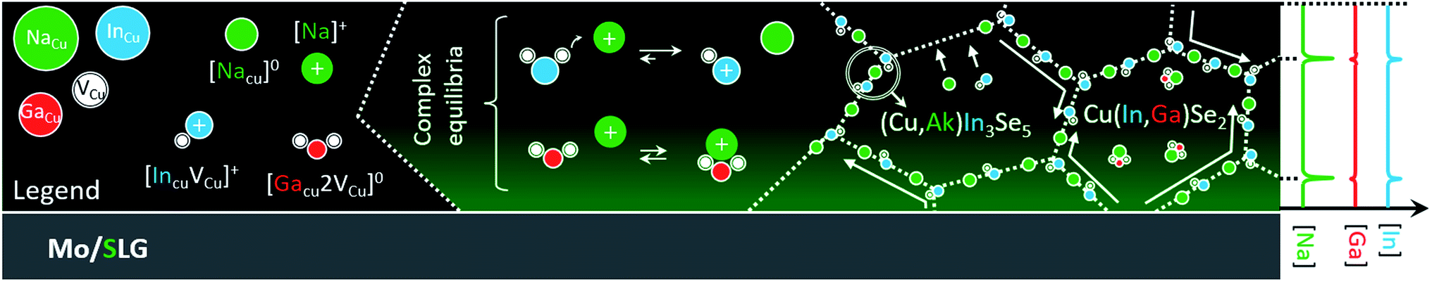 | ||
| Fig. 3 Hypothetical model that attempts to reconcile the findings from polycrystalline and monocrystalline CIGS. From left to right. Legend describing the point defect and defect complexes discussed. Hypothetic effect of sodium doping on the chemical equilibria involving the defect complexes: whereas the more labile {[InCu2+]2[VCu−]} gets dissolved unleashing copper vacancies, the same does not hold for {[GaCu2+]2[VCu−]}. Induced preferential diffusion of indium to CIGS grain boundaries (with formation of Na-rich ODC phase) and retention of gallium at grain interior. The model is tested by DFT and discussed in the text. | ||
The model considers the existence of supercomplex defects,1 as first suggested by Zhang et al. in 1998,78 and detected recently by Stokes et al.79 These complexes are the result of coulombic interaction between copper vacancy acceptors VCu− and indium/gallium on copper antisite donors (In,Ga)Cu2+. The concentration of these complexes is ruled by an equilibrium that depends on the composition of the CIGS matrix (i.e. on the chemical potential of the matrix elements).
The Na incorporation and ensuing capture by CIGS copper vacancies69 may lead to a mass action effect on the chemical equilibria of these complexes. If less vacancies are available for binding, the concentration of the complexes would drop, in accordance to Le Chatelier.
Indeed, Stanbery et al. suggested that Na uptake destabilizes {[InCu2+]2[VCu−]} neutral defects, easing In migration away from CIS bulk.80,81 In the same matrix, the stability of the corresponding Ga complex {[GaCu2+]2[VCu−]} would clearly differ from that of {[InCu2+]2[VCu−]}, due to the smaller Ga radius,82 which should result in different mass transport properties for In and Ga. The binding energy of the analogous Ga complex was reported to be 0.7 eV higher in CuGaSe2 than that of {[InCu2+]2[VCu−]} in CIS.83 It follows that {[GaCu2+]2[VCu−]} should be less susceptible to Na-induced mass action in Ga-rich CIGS, compared to the In complex. The next section reveals if the hypothesis also applies to In and Ga in CIGS having the same composition.
If Na helps to dissolve In complexes, the following effects observed in In-rich CIGS are understood:
(i) Na-induced increased p-type conductivity;30
(ii) In enrichment of grain boundaries, i.e. the consequential passivating character;84
(iii) Na-induced enhanced grain growth.40,42
Furthermore, if Na tends to cluster with Ga into vacancy supercomplexes, the following effects observed in Ga-rich CIGS are understood:
(i) Higher open circuit voltage deficit,85 possibly due to higher compensation and increase of electrostatic potential fluctuations;
(ii) Less frequent Ga enrichment of grain boundaries, i.e. their detrimental nature for device efficiency;43,86
(iii) Na-induced hindered grain growth.26,41,43
A second hypothesis relates to the asymmetry between In and Ga diffusivity, as already suggested by Witte et al. in Na-free CIGS.39 In this sense, the effect of Na on the migration dynamics of In and Ga has never been considered. Does the presence of Na atoms around the In and Ga diffusing species lower the migration barriers, e.g. due to reversible lattice distortions, as proposed in ref. 22? Is the impact equal for In and Ga or does the diffusion asymmetry still hold in the presence of Na dopants?
| Eb([IIICu2+]2[VCu−]) = Ef([IIICu2+]2[VCu−]) − Ef([IIICu2+]) − 2Ef([VCu−]), | (1) |
In order to assess the reliability of the results, several supercell sizes were considered with both the semilocal PBE87 and hybrid HSE06 (ref. 88) (with parameters α = 0.25 and ω = 0.20 Å−1) functionals. The calculations were performed by the VASP program package89,90 ensuring convergence with respect to the plane wave energy cutoff and the k-point sampling. The defect formation energies were obtained by using the equilibrium bulk lattice parameters and eqn (2).
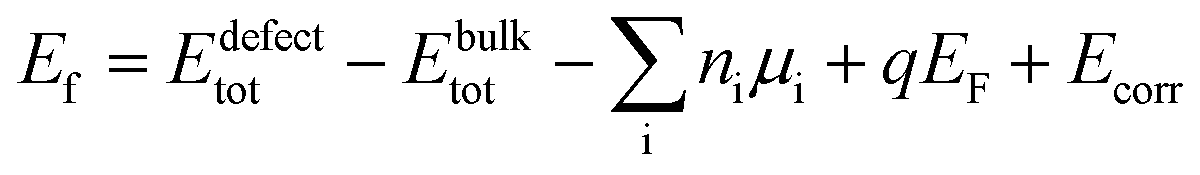 | (2) |
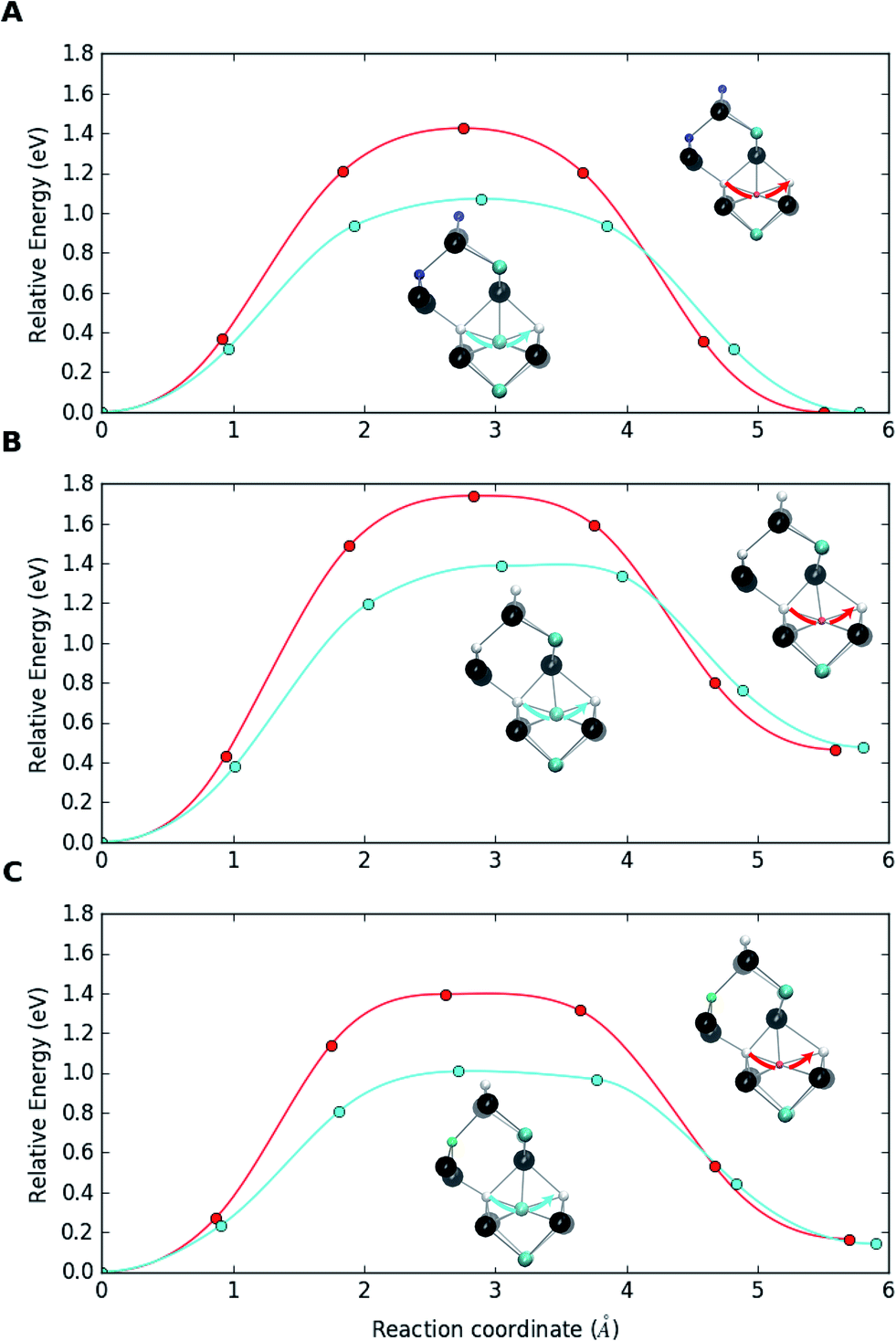 | ||
| Fig. 4 (a) Migration dynamics of Ga atoms (red curves) and In atoms (cyan curves) in bulk CIS through Cu vacancies. (b) Corresponding migration barriers when In and Ga are part of {[(In,Ga)Cu2+]2[VCu−]} defect complexes and (c) in the presence of Na, i.e. as {[(In,Ga)Cu2+][VCu−][Na0Cu]} defect supercomplexes. The structures are shown at the saddle point and truncated for visualization with Cu (blue), In (cyan), Ga (red), Se (black), Na (green) atoms and vacancy sites (white). | ||
The results for the binding energies of the vacancy antisite complexes (Table 1) reveal similar magnitudes and trends obtained with both functionals. The converged binding energies are on the order of −0.6 eV to −0.7 eV and their uncertainty below 0.2 eV. The defect formation energies have converged within 0.1 eV, but their uncertainties do not cancel out when calculating the binding energies. The magnitudes of the binding energies indicate clearly that the complexes are stable, more so, compared to the HSE06 results by Pohl and Albe83 who obtained a value of −0.29 eV using a different method for finite size correction and also a different value for the HSE06 parameter ω.
| Supercell size (atoms) | Complex | PBEa | HSE06b |
|---|---|---|---|
| a Lattice dimensions: a = b = 5.88 Å, c = 5.91 Å. b Lattice dimensions: a = b = 5.82 Å, c = 5.85 Å. | |||
| 64 | [InCu2+]2[VCu−] | −0.41 | −0.35 |
| [GaCu2+]2[VCu−] | −0.52 | −0.47 | |
| 108 | [InCu2+]2[VCu−] | −0.49 | −0.55 |
| [GaCu2+]2[VCu−] | −0.54 | −0.62 | |
| 216 | [InCu2+]2[VCu−] | −0.63 | |
| [GaCu2+]2[VCu−] | −0.67 | ||
Regardless of the absolute magnitude of the complexes binding energies, Table 1 clearly shows that the difference of stability between {[InCu2+]2[VCu−]} and {[GaCu2+]2[VCu−]} calculated by using the two functionals converges consistently towards a value less than 0.1 eV (the complex with Ga being more stable). It follows that the defect equilibria hypothesis cannot be supported on the basis of a large stability difference. The next subsection directs the focus to the differences in migration properties of In and Ga.
Testing the defect migration hypothesis. A series of DFT calculations has been performed for In and Ga migration barriers in bulk CIS within the Cu vacancy mechanism, i.e., an InCu or GaCu at a Cu site jumping to the neighboring Cu vacancy. Comparing the barriers for the two atoms in bulk CIS to those for breaking the {[InCu2+]2[VCu−]} and {[GaCu2+]2[VCu−]} complexes before and after the complex has trapped a substitutional NaCu enables us to draw conclusions about the asymmetry of In and Ga behaviors in interaction with Na. In these heavy calculations the PBE functional and the supercell of 64 atoms had to be used. The diffusion barriers were calculated by employing the climbing image nudged elastic band (CI-NEB) method.92
Fig. 4a shows the migration barriers for In and Ga in bulk Na-free CIS. The heights of the barriers, 1.07 eV and 1.43 eV, respectively, agree very well with those of Witte et al.39 The smaller size of the Ga atom means that it is more deeply bound to the potential minima than the larger In atom, which also explains the higher stability of the complex with Ga. Fig. 4b depicts the situation when an In or Ga antisite of the {[(III)Cu2+]2[VCu−]} complex jumps to a neighboring Cu vacancy. The barriers in this breaking process, 1.39 eV and 1.74 eV, respectively, are clearly larger than those for the bulk migration. This is a consequence of the complexes stability, i.e. of the Coulomb attraction between negative vacancies and positive antisites. Note that, in the reverse process of antisite returning closer to the two vacancies, the barriers are similar to those in the bulk. Finally, Fig. 4c shows the corresponding barriers when the original complexes have trapped a Na atom to become {[(III)Cu2+][VCu−][Na0Cu]} supercomplexes. The breaking barriers, 1.01 eV and 1.40 eV for In and Ga, respectively, are even slightly smaller than the migration barriers in bulk CIS. This indicates that trapping a Na atom makes the complex susceptible to breaking via the Cu vacancy migration process, which releases IIICu2+ to diffuse in the bulk CIS. It should be noted that a sufficient amount of energy could be available for breaking the {[IIICu2+]2[VCu−]} complex, especially for the In case with the lower breaking barrier. Namely, the calculations reveal that trapping an interstitial Na to a Cu vacancy releases ca. 1 eV of energy, nearly irrespective to the environment of the vacancy (Ga or In) and whether the substitutional Na lies next to the complex or is separated from it.
These calculations corroborate the mechanism of dopant-induced migration catalysis proposed in ref. 22, wherein sodium enhances atomic diffusivity of other atoms within the metal sublattice due to the Frank–Turnbull dopant migration. The above migration barrier values extend the asymmetry between In and Ga diffusion in the Cu-deficient CIS matrix also to Na-doped material. This asymmetry should reasonably hold also for standard Ga-poor CIGS and could explain the observed accumulation of In and depletion of Ga at CIGS grain boundaries and surfaces.
The model does not exclude the theory of Na-induced CIS crystallization,74 but offers an additional insight on the root causes of the hampered growth in CGS. Furthermore, the premise offers a convenient explanation for the detrimental nature of the grain boundaries in Ga-rich CIGS, compared to conventional CIGS.43,86
As vacancy antisite complexes are stable, by lowering the In migration barrier, Na allows the In excess to migrate to its equilibrium location (the grain boundaries). This has long been regarded as a beneficial passivating effect, due to band gap widening at grain boundaries and consequent reduction of charge carrier recombination.84
However, even in the presence of Na, the Ga migration barrier remains larger compared to In, favouring the tendency for Ga to stay at grain interior. It follows that grain boundaries remain comparatively poorer from Ga than In. This translates into Ga-poor grain boundaries in Ga-rich CIGS. The consequently reduced band gap widening at grain boundaries is then unable to prevent parasitic Shockley-Read-Hall recombination, giving a possible explanation for the large deficit of open circuit voltage in Ga-rich CIGS.85
Conclusions and outlook
The current CIGS technology relies on accurate Na doping and GGI grading within and across each grain. Na doping hinders In/Ga interdiffusion in polycrystalline films, but can enhance it in monocrystalline films. It appears that Na impedes the diffusion across the grain boundaries, but enhances it within the grains, which is consistent with the micron scale lateral inhomogeneities responsible for band gap fluctuations in early record cells and possibly in current modules.39,61,93Yet, sodium doping of CIGS is responsible for complex diffusion interdependences with matrix elements and heavier alkali metal dopants that are poorly understood.1,8,10,68 This study tackles the diffusivity interdependence between sodium dopants and In/Ga atoms in CIS proposed in ref. 22. It reveals that Cu vacancies cluster with In and Ga antisites but the capture of sodium lowers the corresponding migration barriers of In and Ga. Furthermore, also in Na-doped material, Ga is shown to be a slower diffusing species than In, in line with the evidence of Ga-depleted grain boundaries in CIGS, which is a possible source of SRH recombination in wider-gap CIGS.
More theoretical and experimental efforts devoted to dopant-induced migration catalysis22 will surely benefit not only the CIGS technology, but the chalcogenide materials communities in general, including those working on topological insulators. These communities should find the approach proposed here a useful tool for grain boundary engineering.
Conflicts of interest
There are no conflicts to declare.Acknowledgements
DC wishes to thank several attendees of the 7th World Conference on Photovoltaic Energy Conversion held in 2018 in Hawaii for their interest on an earlier version of this study and/or for fruitful discussions. Particularly: Stefan Paetel (ZSW, Stuttgart), Harvey Guthrey (NREL; Colorado), Nicholas Barreau (University of Nantes), William Shafarman (University of Delaware), Angus Rockett (University of Illinois) and Su-Huai Wei (Beijing Computational Science Research Center). Ingrid Repins (NREL, Colorado) is also acknowledged for sharing her independent In/Ga diffusion model.67 Special thanks go to Karsten Albe (Technische Universität Darmstadt, Germany) for the useful discussions on the DFT calculations convened during Summer 2019. The Fonds National de la Recherche Luxembourg (FNR) is acknowledged for funding this research through the project GALDOCHS (Gas-phase alkali doping of chalcogenide semiconductors, C14/MS/8302176). INL and the European Commission are also acknowledged for funding the Nano Train for Growth II project no. 713640 through the Marie Curie Cofund programme.Notes and references
- D. Colombara, F. Werner, T. Schwarz, I. C. Infante, Y. Fleming, N. Valle, C. Spindler, E. Vacchieri, G. Rey, M. Guennou, M. Bouttemy, A. Garzón Manjón, I. Peral Alonso, M. Melchiorre, B. El Adib, B. Gault, D. Raabe, P. J. Dale and S. Siebentritt, Nat. Commun., 2018, 9, 826 CrossRef PubMed.
- Solar Frontier Achieves World Record Thin-Film Solar Cell Efficiency of 23.35%, http://www.solar-frontier.com/eng/news/2019/<?pdb_no 0117?>0117<?pdb END?>_press.html, accessed January 29, 2019 Search PubMed.
- V. Bermudez and A. Perez-Rodriguez, Nat. Energy, 2018, 3, 466–475 CrossRef CAS.
- S. Nishiwaki, S. Siebentritt, P. Walk and M. Ch. Lux-Steiner, Progress in Photovoltaics: Research and Applications, 2003, 11, 243–248 CrossRef CAS.
- L. L. Kazmerski, Research cell efficiency records, 2018 Search PubMed.
- M. Contreras, J. Tuttle, D. Du, Y. Qi, A. Swartzlander, A. Tennant and R. Noufi, Appl. Phys. Lett., 1993, 63, 1824–1826 CrossRef CAS.
- J. Hedström, H. Ohlsen, M. Bodegard, A. Kylner, L. Stolt, D. Hariskos, M. Ruckh and H. Schock, ZnO/CdS/Cu(In,Ga)Se/sub 2/ thin film solar cells with improved performance, Proceedings of the 23rd IEEE Photovoltaic Specialists Conference – 1993 (Cat. No. 93CH3283-9), IEEE, Louisville, KY, USA, 1993, pp. 364–371, DOI:10.1109/pvsc.1993.347154.
- A. Chirilă, S. Buecheler, F. Pianezzi, P. Bloesch, C. Gretener, A. R. Uhl, C. Fella, L. Kranz, J. Perrenoud, S. Seyrling, R. Verma, S. Nishiwaki, Y. E. Romanyuk, G. Bilger and A. N. Tiwari, Nat. Mater., 2011, 10, 857–861 CrossRef PubMed.
- P. Jackson, D. Hariskos, R. Wuerz, W. Wischmann and M. Powalla, Phys. Status Solidi RRL, 2014, 8, 219–222 CrossRef CAS.
- C. P. Muzzillo, Sol. Energy Mater. Sol. Cells, 2017, 172, 18–24 CrossRef CAS.
- P. Jackson, D. Hariskos, R. Wuerz, O. Kiowski, A. Bauer, T. M. Friedlmeier and M. Powalla, Phys. Status Solidi RRL, 2015, 9, 28–31 CrossRef CAS.
- R. Wuerz, A. Eicke, F. Kessler, S. Paetel, S. Efimenko and C. Schlegel, Sol. Energy Mater. Sol. Cells, 2012, 100, 132–137 CrossRef CAS.
- C.-H. Cai, R.-Z. Chen, T.-S. Chan, Y.-R. Lu, W.-C. Huang, C.-C. Yen, K. Zhao, Y.-C. Lo and C.-H. Lai, Nano Energy, 2018, 47, 393–400 CrossRef CAS.
- A. Chirilă, P. Reinhard, F. Pianezzi, P. Bloesch, A. R. Uhl, C. Fella, L. Kranz, D. Keller, C. Gretener, H. Hagendorfer, D. Jaeger, R. Erni, S. Nishiwaki, S. Buecheler and A. N. Tiwari, Nat. Mater., 2013, 12, 1107–1111 CrossRef PubMed.
- P. Pistor, D. Greiner, C. A. Kaufmann, S. Brunken, M. Gorgoi, A. Steigert, W. Calvet, I. Lauermann, R. Klenk, T. Unold and M.-C. Lux-Steiner, Appl. Phys. Lett., 2014, 105, 063901 CrossRef.
- P. Reinhard, B. Bissig, F. Pianezzi, E. Avancini, H. Hagendorfer, D. Keller, P. Fuchs, M. Döbeli, C. Vigo, P. Crivelli, S. Nishiwaki, S. Buecheler and A. N. Tiwari, Chem. Mater., 2015, 27, 5755–5764 CrossRef CAS.
- S. Siebentritt, E. Avancini, M. Bär, J. Bombsch, E. Bourgeois, S. Buecheler, R. Carron, C. Castro, S. Duguay, R. Félix, E. Handick, D. Hariskos, V. Havu, P. Jackson, H.-P. Komsa, T. Kunze, M. Malitckaya, R. Menozzi, M. Nesladek, N. Nicoara, M. Puska, M. Raghuwanshi, P. Pareige, S. Sadewasser, G. Sozzi, A. N. Tiwari, S. Ueda, A. Vilalta-Clemente, T. P. Weiss, F. Werner, R. G. Wilks, W. Witte and M. H. Wolter, Adv. Energy Mater., 2020, 10, 1903752 CrossRef CAS.
- G. Gregori, R. Merkle and J. Maier, Prog. Mater. Sci., 2017, 89, 252–305 CrossRef CAS.
- A. Laemmle, R. Wuerz, T. Schwarz, O. Cojocaru-Mirédin, P.-P. Choi and M. Powalla, J. Appl. Phys., 2014, 115, 154501 CrossRef.
- B. A. Grzybowski, A. Winkleman, J. A. Wiles, Y. Brumer and G. M. Whitesides, Nat. Mater., 2003, 2, 241–245 CrossRef CAS PubMed.
- S. Deutschländer, C. Boitard, G. Maret and P. Keim, Phys. Rev. E: Stat., Nonlinear, Soft Matter Phys., 2015, 92, 060302 CrossRef PubMed.
- D. Colombara, Phys. Rev. Mater., 2019, 3, 054602 CrossRef CAS.
- I. Repins, M. A. Contreras, B. Egaas, C. DeHart, J. Scharf, C. L. Perkins, B. To and R. Noufi, Progress in Photovoltaics: Research and Applications, 2008, 16, 235–239 CrossRef CAS.
- P. Jackson, R. Wuerz, D. Hariskos, E. Lotter, W. Witte and M. Powalla, Phys. Status Solidi RRL, 2016, 10, 583–586 CrossRef CAS.
- J. E. Granata, J. R. Sites, S. Asher and R. J. Matson, in Conference Record of the Twenty Sixth IEEE Photovoltaic Specialists Conference – 1997, 1997, pp. 387–390 Search PubMed.
- D. Rudmann, A. F. da Cunha, M. Kaelin, F. Kurdesau, H. Zogg, A. N. Tiwari and G. Bilger, Appl. Phys. Lett., 2004, 84, 1129–1131 CrossRef CAS.
- L. Kronik, D. Cahen and H. W. Schock, Adv. Mater., 1998, 10, 31–36 CrossRef CAS.
- D. W. Niles, K. Ramanathan, F. Hasoon, R. Noufi, B. J. Tielsch and J. E. Fulghum, J. Vac. Sci. Technol., A, 1997, 15, 3044–3049 CrossRef CAS.
- S.-H. Wei, S. B. Zhang and A. Zunger, J. Appl. Phys., 1999, 85, 7214–7218 CrossRef CAS.
- Z. Yuan, S. Chen, Y. Xie, J.-S. Park, H. Xiang, X.-G. Gong and S.-H. Wei, Adv. Energy Mater., 2016, 6, 1601191 CrossRef.
- D. Rudmann, G. Bilger, M. Kaelin, F. J. Haug, H. Zogg and A. N. Tiwari, Thin Solid Films, 2003, 431–432, 37–40 CrossRef CAS.
- D. Rudmann, M. Kaelin, F. J. Haug, F. Kurdesau, H. Zogg and A. N. Tiwari, in Proceedings of 3rd World Conference on Photovoltaic Energy Conversion, 2003, 2003, vol. 1, pp. 376–379 Search PubMed.
- O. Lundberg, J. Lu, A. Rockett, M. Edoff and L. Stolt, J. Phys. Chem. Solids, 2003, 64, 1499–1504 CrossRef CAS.
- D. Rudmann, D. Brémaud, H. Zogg and A. N. Tiwari, J. Appl. Phys., 2005, 97, 084903 CrossRef.
- F. Hergert, S. Jost, R. Hock, M. Purwins and J. Palm, Thin Solid Films, 2007, 515, 5843–5847 CrossRef CAS.
- R. Caballero, C. A. Kaufmann, T. Eisenbarth, M. Cancela, R. Hesse, T. Unold, A. Eicke, R. Klenk and H. W. Schock, Thin Solid Films, 2009, 517, 2187–2190 CrossRef CAS.
- D. Güttler, A. Chirila, S. Seyrling, P. Blösch, S. Buecheler, X. Fontané, V. Izquierdo-Roca, L. Calvo-Barrio, A. Peréz-Rodriguez, J. R. Morante, A. Eicke and A. N. Tiwari, in 2010 35th IEEE Photovoltaic Specialists Conference (PVSC), Institute of Electrical and Electronics Engineers, Hawaiian Convention CenterHonolulu, HI, USA, 2010, pp. 003420–003424 Search PubMed.
- H. Rodriguez-Alvarez, R. Mainz, R. Caballero, D. Abou-Ras, M. Klaus, S. Gledhill, A. Weber, C. A. Kaufmann and H.-W. Schock, Sol. Energy Mater. Sol. Cells, 2013, 116, 102–109 CrossRef CAS.
- W. Witte, D. Abou-Ras, K. Albe, G. H. Bauer, F. Bertram, C. Boit, R. Brüggemann, J. Christen, J. Dietrich, A. Eicke, D. Hariskos, M. Maiberg, R. Mainz, M. Meessen, M. Müller, O. Neumann, T. Orgis, S. Paetel, J. Pohl, H. Rodriguez-Alvarez, R. Scheer, H.-W. Schock, T. Unold, A. Weber and M. Powalla, Progress in Photovoltaics: Research and Applications, 2015, 23, 717–733 CrossRef CAS.
- V. Probst, J. Rimmasch, W. Riedl, W. Stetter, J. Holz, H. Harms and F. Karg, The impact of controlled sodium incorporation on rapid thermal processed Cu(InGa)Se2 thin films and devices, Proceedings of 1994 IEEE 1st World Conference on Photovoltaic Energy Conversion – WCPEC (A Joint Conference of PVSC, PVSEC and PSEC), Waikoloa, HI, USA, 1994, vol. 1, pp. 144–147, DOI:10.1109/wcpec.1994.519828.
- A. Rockett, J. S. Britt, T. Gillespie, C. Marshall, M. M. Al Jassim, F. Hasoon, R. Matson and B. Başol, Thin Solid Films, 2000, 372, 212–217 CrossRef CAS.
- Q. Guo, G. M. Ford, R. Agrawal and H. W. Hillhouse, Progress in Photovoltaics: Research and Applications, 2013, 21, 64–71 CrossRef CAS.
- M. Raghuwanshi, E. Cadel, P. Pareige, S. Duguay, F. Couzinie-Devy, L. Arzel and N. Barreau, Appl. Phys. Lett., 2014, 105, 013902 CrossRef.
- T.-Y. Lin, C.-H. Chen, L.-W. Wang, W.-C. Huang, Y.-W. Jheng and C.-H. Lai, Nano Energy, 2017, 41, 697–705 CrossRef CAS.
- D. J. Schroeder and A. A. Rockett, J. Appl. Phys., 1997, 82, 4982–4985 CrossRef CAS.
- A. M. Gabor, J. R. Tuttle, D. S. Albin, M. A. Contreras, R. Noufi and A. M. Hermann, Appl. Phys. Lett., 1994, 65, 198–200 CrossRef CAS.
- M. A. Contreras, A. M. Gabor, A. L. Tennant, S. Asher, J. Tuttle and R. Noufi, Progress in Photovoltaics: Research and Applications, 1994, 2, 287–292 CrossRef CAS.
- M. A. Contreras, J. Tuttle, A. Gabor, A. Tennant, K. Ramanathan, S. Asher, A. Franz, J. Keane, L. Wang, J. Scofield and R. Noufi, in IEEE Photovoltaic Specialists Conference - 1994, 1994 IEEE First World Conference on Photovoltaic Energy Conversion, 1994, Conference Record of the Twenty Fourth, vol. 1, pp. 68–75 Search PubMed.
- A. M. Gabor, J. R. Tuttle, M. H. Bode, A. Franz, A. L. Tennant, M. A. Contreras, R. Noufi, D. G. Jensen and A. M. Hermann, Sol. Energy Mater. Sol. Cells, 1996, 41–42, 247–260 CrossRef.
- B. M. Başol, V. K. Kapur, A. Halani, C. R. Leidholm, J. Sharp, J. R. Sites, A. Swartzlander, R. Matson and H. Ullal, J. Vac. Sci. Technol., A, 1996, 14, 2251–2256 CrossRef.
- F. Karg, Energy Procedia, 2012, 15, 275–282 CrossRef CAS.
- D. G. Moon, J. H. Yun, J. Gwak, S. Ahn, A. Cho, K. Shin, K. Yoon and S. Ahn, Energy Environ. Sci., 2012, 5, 9914–9921 RSC.
- I. Repins, L. Mansfield, A. Kanevce, S. A. Jensen, D. Kuciauskas, S. Glynn, T. Barnes, W. Metzger, J. Burst, C. S. Jiang, P. Dippo, S. Harvey, G. Teeter, C. Perkins, B. Egaas, A. Zakutayev, J. H. Alsmeier, T. Lußky, L. Korte, R. G. Wilks, M. Bär, Y. Yan, S. Lany, P. Zawadzki, J. S. Park and S. Wei, in 2016 IEEE 43rd Photovoltaic Specialists Conference (PVSC), 2016, pp. 0309–0314 Search PubMed.
- S. Siebentritt, Sol. Energy Mater. Sol. Cells, 2011, 95, 1471–1476 CrossRef CAS.
- J. H. Werner, J. Mattheis and U. Rau, Thin Solid Films, 2005, 480–481, 399–409 CrossRef CAS.
- J. Mattheis, U. Rau and J. H. Werner, J. Appl. Phys., 2007, 101, 113519 CrossRef.
- M. Bokalič, A. Gerber, B. E. Pieters, U. Rau and M. Topič, IEEE Journal of Photovoltaics, 2018, 8, 272–277 Search PubMed.
- U. Rau and J. H. Werner, Appl. Phys. Lett., 2004, 84, 3735–3737 CrossRef CAS.
- D. Colombara, U. Berner, A. Ciccioli, J. C. Malaquias, T. Bertram, A. Crossay, M. Schöneich, H. J. Meadows, D. Regesch, S. Delsante, G. Gigli, N. Valle, J. Guillot, B. E. Adib, P. Grysan and P. J. Dale, Sci. Rep., 2017, 7, 43266 CrossRef PubMed.
- L. E. Oikkonen, M. G. Ganchenkova, A. P. Seitsonen and R. M. Nieminen, J. Appl. Phys., 2013, 114, 083503 CrossRef.
- K. Bothe, G. H. Bauer and T. Unold, Thin Solid Films, 2002, 403–404, 453–456 CrossRef CAS.
- A. Laemmle, R. Wuerz and M. Powalla, Thin Solid Films, 2015, 582, 27–30 CrossRef CAS.
- V. Gusak, O. Lundberg, E. Wallin, S.-O. Katterwe, U. Malm and L. Stolt, Optimization of alkali supply and Ga/(Ga+In) evaporation profile for thin (0.5 μm) CIGS solar cells. Proceedings of the 2018 IEEE 7th World Conference on Photovoltaic Energy Conversion (WCPEC) (A Joint Conference of 45th IEEE PVSC, 28th PVSEC & 34th EU PVSEC), Waikoloa, HI, USA, 2018, pp. 1641–1644, DOI:10.1109/pvsc.2018.8548188.
- A. Duchatelet, K. Nguyen, P.-P. Grand, D. Lincot and M. Paire, Appl. Phys. Lett., 2016, 109, 253901 CrossRef.
- D. Correia, D. Siopa, D. Colombara, S. Tombolato, P. M. P. Salomé, K. Abderrafi, P. Anacleto, P. J. Dale and S. Sadewasser, Results Phys., 2019, 12, 2136–2140 CrossRef.
- D. J. Schroeder, G. D. Berry and A. A. Rockett, Appl. Phys. Lett., 1996, 69, 4068–4070 CrossRef CAS.
- I. L. Repins, S. Harvey, K. Bowers, S. Glynn and L. M. Mansfield, MRS Adv., 2017, 2, 3169–3174 CrossRef CAS.
- L. Stolt, E. Wallin, S. Sodergen, T. Jarmar and M. Edoff, presented in part at the Materials Research Society Meeting, Phoenix, April 2017 Search PubMed.
- T. Maeda, A. Kawabata and T. Wada, Jpn. J. Appl. Phys., 2015, 54, 08KC20 CrossRef.
- M. Malitckaya, H.-P. Komsa, V. Havu and M. J. Puska, J. Phys. Chem. C, 2017, 121, 15516–15528 CrossRef CAS.
- Y. Sun, S. Lin, W. Li, S. Cheng, Y. Zhang, Y. Liu and W. Liu, Engineering, 2017, 3, 452–459 CrossRef CAS.
- S. Li, S. Wang, D.-M. Tang, W. Zhao, H. Xu, L. Chu, Y. Bando, D. Golberg and G. Eda, Applied Materials Today, 2015, 1, 60–66 CrossRef.
- D. Braunger, D. Hariskos, G. Bilger, U. Rau and H. W. Schock, Thin Solid Films, 2000, 361–362, 161–166 CrossRef CAS.
- A. Brummer, V. Honkimäki, P. Berwian, V. Probst, J. Palm and R. Hock, Thin Solid Films, 2003, 437, 297–307 CrossRef CAS.
- J. Nishinaga, T. Nagai, T. Sugaya, H. Shibata and S. Niki, Appl. Phys. Express, 2018, 11, 082302 CrossRef.
- E. Avancini, D. Keller, R. Carron, Y. A.-R. Dasilva, R. Erni, A. Priebe, S. D. Napoli, M. Carrisi, G. Sozzi, R. Menozzi, F. Fu, S. Buecheler and A. N. Tiwari, Sci. Technol. Adv. Mater., 2018, 19, 871–882 CrossRef CAS PubMed.
- O. Cojocaru-Mirédin, P. Choi, R. Wuerz and D. Raabe, Ultramicroscopy, 2011, 111, 552–556 CrossRef PubMed.
- S. B. Zhang, S.-H. Wei, A. Zunger and H. Katayama-Yoshida, Phys. Rev. B: Condens. Matter Mater. Phys., 1998, 57, 9642 CrossRef CAS.
- A. Stokes, M. Al-Jassim, D. R. Diercks, B. Egaas and B. Gorman, Acta Mater., 2016, 102, 32–37 CrossRef CAS.
- B. J. Stanbery, S. Kincal, S. Kim, T. J. Anderson, O. D. Crisalle, S. P. Ahrenkiel and G. Lippold, in Conference Record of the Twenty-Eighth IEEE Photovoltaic Specialists Conference, 2000, Anchorage, AK,USA, 2000, pp. 440–445 Search PubMed.
- B. J. Stanbery, Crit. Rev. Solid State Mater. Sci., 2002, 27, 73–117 CrossRef CAS.
- L. H. Ahrens, Geochim. Cosmochim. Acta, 1952, 2, 155–169 CrossRef CAS.
- J. Pohl and K. Albe, Phys. Rev. B: Condens. Matter Mater. Phys., 2013, 87, 245203 CrossRef.
- D. Keller, S. Buecheler, P. Reinhard, F. Pianezzi, B. Bissig, R. Carron, F. Hage, Q. Ramasse, R. Erni and A. N. Tiwari, Appl. Phys. Lett., 2016, 109, 153103 CrossRef.
- F. Larsson, N. S. Nilsson, J. Keller, C. Frisk, V. Kosyak, M. Edoff and T. Törndahl, Progress in Photovoltaics: Research and Applications, 2017, 25, 755–763 CrossRef CAS.
- B. M. West, M. Stuckelberger, H. Guthrey, L. Chen, B. Lai, J. Maser, V. Rose, W. Shafarman, M. Al-Jassim and M. I. Bertoni, Nano Energy, 2017, 32, 488–493 CrossRef CAS.
- J. P. Perdew, K. Burke and M. Ernzerhof, Phys. Rev. Lett., 1996, 77, 3865–3868 CrossRef CAS PubMed.
- J. Heyd, G. E. Scuseria and M. Ernzerhof, J. Chem. Phys., 2003, 118, 8207–8215 CrossRef CAS.
- G. Kresse and J. Furthmüller, Phys. Rev. B: Condens. Matter Mater. Phys., 1996, 54, 11169 CrossRef CAS.
- G. Kresse and J. Furthmüller, Comput. Mater. Sci., 1996, 6, 15–50 CrossRef CAS.
- C. Freysoldt, J. Neugebauer and C. G. V. de Walle, Phys. Status Solidi B, 2011, 248, 1067–1076 CrossRef CAS.
- G. Henkelman and H. Jónsson, J. Chem. Phys., 2000, 113, 9978–9985 CrossRef CAS.
- D. Eich, U. Herber, U. Groh, U. Stahl, C. Heske, M. Marsi, M. Kiskinova, W. Riedl, R. Fink and E. Umbach, Thin Solid Films, 2000, 361–362, 258–262 CrossRef CAS.
Footnote |
| † Electronic supplementary information (ESI) available. See DOI: 10.1039/d0ta01103g |
| This journal is © The Royal Society of Chemistry 2020 |