
 Open Access Article
 This Open Access Article is licensed under a
 Creative Commons Attribution 3.0 Unported Licence
The role of ultra-thin MnOx co-catalysts on the photoelectrochemical properties of BiVO4 photoanodes†
Rowshanak
Irani
,
Paul
Plate
,
Christian
Höhn
,
Peter
Bogdanoff
,
Markus
Wollgarten
 ,
Katja
Höflich
,
Roel
van de Krol
and
Fatwa F.
Abdi
*
,
Katja
Höflich
,
Roel
van de Krol
and
Fatwa F.
Abdi
*
Institute for Solar Fuels, Helmholtz-Zentrum Berlin für Materialien und Energie GmbH, Hahn-Meitner-Platz 1, Berlin 14109, Germany. E-mail: fatwa.abdi@helmholtz-berlin.de
First published on 24th February 2020
Abstract
Metal oxide semiconductors are promising as photoanodes for solar water splitting, but they typically suffer from poor charge transfer properties due to the slow surface reaction kinetics for oxygen evolution. To overcome this, their surfaces are usually modified by depositing earth-abundant, efficient, and inexpensive water oxidation co-catalysts. While this effort has been successful in enhancing the photoelectrochemical performance, a true understanding of the nature of the improvement is still under discussion. This is due to the fact that the co-catalyst can have multiple functionalities, e.g., accelerating charge transfer, passivating surface states, or modifying band bending. Disentangling these factors is challenging, but necessary to obtain a full understanding of the enhancement mechanism and better design the semiconductor/co-catalyst interface. In this study, we investigate the role of atomic layer deposited (ALD) MnOx co-catalysts and their thickness in the photoelectrochemical performance of BiVO4 photoanodes. Modified MnOx/BiVO4 samples with an optimum thickness of ∼4 nm show higher photocurrent (a factor of >3) as well as lower onset potential (by ∼100 mV) compared to the bare BiVO4. We combine spectroscopic and photoelectrochemical measurements to unravel the different roles of MnOx and explain the photocurrent trend as a function of the thickness of MnOx. X-ray photoelectron spectroscopy (XPS) studies reveal that the surface band bending of BiVO4 is modified after the addition of MnOx, therefore reducing surface recombination. At the same time, increasing the thickness of MnOx beyond the optimal 4 nm provides shunting pathways, as shown by energy dispersive X-ray scanning transmission electron microscopy (EDX-STEM) and redox electrochemistry. This cancels out the band bending effect, which explains the observed photocurrent trend. Therewith, this study provides additional insights into the understanding of the charge transfer processes occurring at the semiconductor–catalyst interface.
Introduction
Photoelectrochemical (PEC) water splitting is an attractive method to harvest solar energy and store it in the form of chemical bonds (i.e., H2 and O2).1–3 Among the two half-reactions, oxygen evolution is typically the limiting one due to the more kinetically demanding nature of the reaction.4 Therefore, significant efforts have been dedicated to the development of efficient photoanodes to drive this reaction. Metal oxides are widely used as photoanode materials due to their low costs, general stability and scalable preparation techniques. However, their performance is often limited by poor surface charge transfer properties due to low catalytic activity and/or high surface recombination.5–8 To overcome this, various co-catalysts, e.g., RuO2, Ni/FeOOH, NiFeOx, CoPi, MnOx, etc. have been applied in order to modify the surface of metal oxide semiconductors,9–16 which resulted in an improvement of the photocurrent.14,17–25 Indeed, most metal oxide photoanodes showing high photocurrent (>5 mA cm−2) are decorated with additional co-catalysts.16,26,27One of the key parameters in the optimization of a semiconductor/co-catalyst interface is the thickness of the co-catalyst. Various reports have shown that there exists an optimal thickness at which the photocurrent of the semiconductor/co-catalyst photoanode is maximized.28,29 This behavior has been attributed to a few factors, e.g., trade-off between higher catalytic activity and parasitic absorption or resistivity in thicker co-catalysts, but no clear evidence was provided up to now. In addition, despite the improvement observed with co-catalyst deposition on metal oxide photoanodes, the true role of the co-catalysts is still under debate. Already, in 2012, Gamelin pointed out conflicting proposed mechanisms for photocurrent enhancement in CoPi/hematite photoanode systems.30 More recently, differing mechanisms were also reported for CoPi/BiVO4 photoanode systems. Photoinduced absorption spectroscopy (PIA)31 and intensity modulated photocurrent spectroscopy (IMPS)32 studies concluded that CoPi passivates surface states on BiVO4, but dual working-electrode voltammetry measurements showed that CoPi also has a true catalytic role on BiVO4.33 The considerations above, therefore, clearly illustrate that we still need additional well-designed studies in order to fully unravel the role of co-catalysts on semiconductor photoanodes for water oxidation. In this work, we investigate the role of ultra-thin MnOx co-catalysts on spray-deposited BiVO4 photoanodes. Spray-deposited BiVO4 is among the best performing non-nanostructured BiVO4 photoelectrodes,23,34–36 and the scalability of the process has been demonstrated.37 Earth-abundant and inexpensive MnOx has been shown to demonstrate a particularly promising behavior and low overpotential when deposited on BiVO4.38,39 Here, by using atomic layer deposition (ALD), we carefully control the thickness of the MnOx co-catalysts and examine the PEC properties of the resulting MnOx/BiVO4 photoanodes. The photocurrent is maximized when the thickness of MnOx is 4 nm. By examining the interface properties between MnOx and BiVO4 using a combination of spectroscopy, (photo)electrochemical and microscopy techniques, we are able to show that increasing the thickness of MnOx results in decreasing surface recombination due to higher band bending, but also in the creation of shunting pathways due to direct contact between the MnOx and the conducting substrates (FTO) at pinholes. These two competing effects, therefore, result in a trade-off, which fully explains the observed photocurrent trend.
Experimental
Deposition of BiVO4 thin film photoanodes
BiVO4 thin films were deposited using spray pyrolysis.23,40–42 Commercial FTO-coated glass slides (fluorine-doped tin dioxide, 15 Ω □−1, TEC-15, Pilkington) were used as the substrates. Prior to the deposition, a three-step cleaning procedure of ultrasonication in 10 vol% Triton™ X-100 solution (Sigma Aldrich), acetone, and ethanol, each for 15 minutes, was followed. A thin interfacial layer of SnO2 was first deposited as a hole blocking layer43 on the FTO substrates using 5 mL solution of 0.1 M SnCl4 (98%, Aldrich) in ethyl acetate (99.8%, VWR Chemical). The solution was sprayed onto the substrates using a Quickmist air atomizing spray nozzle (1/4QMJAU-NC + SUQR-200). The distance between the spray nozzle and the substrate, which was placed on a hot plate, was 20 cm. To ensure adequate solvent evaporation a pulsed spray mode was used; 5 s of spraying was followed by a 53 s delay. The BiVO4 precursor solution was prepared by dissolving 4 mmol Bi(NO3)3·5H2O (98%, Alfa Aesar) in acetic acid (99.8%, Sigma Aldrich), while 4 mmol VO(AcAc)2 (99%, Acros Organics) was dissolved separately in absolute ethanol (VWR Chemicals). Each solution was ultrasonicated for 15 minutes, then mixed, and finally ultrasonicated again for 15 minutes. The ratio of the acetic acid and absolute ethanol was 1![[thin space (1/6-em)]](https://www.rsc.org/images/entities/char_2009.gif) :9 in the final 100 mL solution. The hot plate temperature was kept constant at 425 °C for the SnO2 deposition and then increased to 450 °C for the BiVO4 deposition. In order to improve the crystallinity, following the deposition, all samples were annealed in air at 460 °C for 2 hours.
:9 in the final 100 mL solution. The hot plate temperature was kept constant at 425 °C for the SnO2 deposition and then increased to 450 °C for the BiVO4 deposition. In order to improve the crystallinity, following the deposition, all samples were annealed in air at 460 °C for 2 hours.
Deposition of MnOx co-catalysts
Manganese oxide (MnOx) thin films were deposited using a home-built, hot-wall atomic layer deposition (ALD) reactor.44 The ALD reactor was constantly pumped by using a turbo molecular pump, backed-up with a roughing pump. The BiVO4 substrates were mounted on a sample carrier, which is directly placed on the substrate heater in the ALD reactor. Bis(cyclopentadienyl)manganese ((EtCp2)Mn, Strem Chemicals, 98%), kept at 85 °C was used as the Mn precursor, and water (Millipore, 18.2 MΩ) as the oxygen source. The reactor wall was heated to 125 °C, while the substrate temperature was kept at 150 °C. The Mn precursor and the water dosing steps were performed each for 1.5 s. After each of these dosing steps, a pump/purge/pump step was carried out, consisting of 30 s pumping/0.1 s Ar dose/30 s pumping. This led to a growth per cycle (GPC) of 1.3 Å. The film thicknesses were determined by ex situ spectroscopic ellipsometry (J.A. Woollam Co. spectroscopic ellipsometer, M-2000D, 193–1000 nm) on a silicon reference sample placed next to the BiVO4 substrates during the deposition. The dielectric function of the MnOx film was modeled with a Tauc–Lorentz dispersion equation.45Materials characterization
X-ray diffraction (XRD) measurements were done using a Bruker D8 diffractometer with Cu Kα radiation at 40 kV and 40 mA. UV-Vis spectra were measured using a PerkinElmer Lambda 950 spectrophotometer equipped with an integrating sphere. The films were placed inside the integrating sphere with a center mount sample holder (positioned at ∼7.5° offset from the incident light) to measure transflectance (TR), which is the sum of transmittance (T) and reflectance (R). Scanning helium ion microscopy (HIM) images were obtained with a Zeiss Orion Nanofab equipped with a secondary electron detector. HIM allows for high-resolution imaging of weakly or non-conductive nanosized features requiring a large depth of focus. The He gas pressure was set to 2 × 10⁻⁶ Torr for an acceleration voltage of 30 kV, probe currents ranging from 0.1 to 0.3 pA and a high spot control number to minimize the beam divergence. Monochromatic Al Kα radiation (hν = 1486.74 eV, SPECS FOCUS 500 monochromator) was used for X-ray photoelectron spectroscopy (XPS, SPECS PHOIBOS 100 analyzer) measurements. The pass energy was set to 30 and 10 eV with step sizes of 0.5 and 0.05 eV for the survey and fine spectra, respectively. The peaks were fitted in XPSPEAK software, using Voigt profiles and a Shirley background subtraction. All spectra were calibrated with respect to the adventitious carbon C 1s peak at 284.5 eV. Samples for observation in the cross section were prepared by using a Zeiss Crossbeam 340 focused ion beam system. Elemental distribution maps were obtained using a Zeiss LIBRA 200 FE transmission electron microscope operated at 200 kV accelerating voltage in scanning mode using a Thermo Fisher energy dispersive X-ray (EDX) spectrometer. The data shown here represent the net count signal after spectral deconvolution with an averaging kernel of 3 × 3 pixels.Photoelectrochemical characterization
A three-electrode configuration using a custom Teflon cell (sample area = 0.283 cm2) was applied for photoelectrochemical measurements.46 The photoelectrochemical experiments were performed in a 0.1 M potassium phosphate buffer (KPi, pH ∼ 7) electrolyte. The buffer solution was prepared by mixing 4.625 g of potassium phosphate monobasic (KH2PO4, 99.5%, Merck) and 15.05 g of potassium hydrogen phosphate trihydrate (K2HPO4·3H2O, 99%, Merck) in 1 L of Milli-Q water (18.2 MΩ cm). A Solartron SI 1286 potentiostat was used to control the potential of the working electrode. The reference electrode was an Ag/AgCl electrode (XR300, saturated KCl solution, Radiometer Analytical) and the counter electrode was a Pt wire. A blue 455 nm LED (Thorlabs M455L3, 20 mW cm−2) was used as the light source. Potential conversion into the reversible hydrogen electrode (RHE) scale with respect to the Ag/AgCl potential was calculated using the Nernst equation:| VRHE = VAg/AgCl + 0.0591 × pH + V0Ag/AgCl | (1) |
Electrochemical mass spectrometry (EMS) was used for the detection of O2 evolution. The measurements were carried out in a PEC cell with ∼200 μm electrolyte layers between the BiVO4/MnOx photoanode and a gas-permeable membrane (ethylene–tetrafluoroethylene copolymer, Scimat), which serves as an inlet system to the differential pumped mass spectrometer system. A variable leak valve connected the first vacuum chamber to the second high-vacuum chamber, which housed the quadrupole mass spectrometer (Pfeiffer Vacuum, QMG 220 M1). Gaseous or volatile compounds formed by the photoanode were collected through the permeable membrane and detected using the mass spectrometer. Ag/AgCl was used as the reference electrode and Pt wire as the counter electrode. To calibrate the PEC cell, measurements were done with a Pt sheet as the working electrode, which is assumed to have a faradaic efficiency of 100% for the oxygen evolution reaction. A Newport solar simulator was used as the illumination source. The light power was adjusted using a calibrated spectrometer (USB2000, Ocean Optics) to 650 mW cm−2 for light wavelengths between 400 and 900 nm.
Intensity modulated photocurrent spectroscopy (IMPS) measurements were performed in an applied bias range of 0.6 to 1.6 VRHE and in a frequency range of 100 mHz to 100 kHz. A frequency response analyzer (FRA, Solartron 1250, Schlumberger) connected to an LED driver (Thorlabs DC2100) was used in order to sinusoidally modulate the light intensity of the same blue LED source (455 nm, Thorlabs M455L3). The rms amplitude was 2 mW cm−2, which was superimposed on a 20 mW cm−2 DC background intensity. A beam splitter was used to split the light into two beams directing towards the PEC cell and a high-speed Si photodiode (Thorlabs PDA10A-EC). The current monitor output of the as-mentioned potentiostat and the voltage signal of the high-speed Si photodiode were connected to the two channels of the FRA. The real and imaginary components of the opto-electrical gain of the sample obtained by dividing the measured photocurrent density (jphoto) through the voltage of the Si photodiode were obtained using the FRA. The absolute (dimensionless) complex gain of the photoelectrode was converted by multiplying with a conversion factor (0.015 V cm2 mA−1), which was determined by measuring the absolute light intensity using a calibrated photodiode (PD300UV + Ophir Nova II) and the voltage of the high-speed Si photodiode. The IMPS theory and measurement are explained in detail elsewhere.47 Analysis steps, as described in the literature,32,47 were applied in order to extract the charge transfer (ktr) and surface recombination (krec) rate constants. From these two values, the charge transfer efficiency (ηCT), which can be described as the fraction of the holes that arrive at the surface and are injected into the electrolyte, was calculated using the following equation:
 | (2) |
Electrochemical impedance spectroscopy (EIS) measurements were conducted under the same blue LED illumination between 0.6 and 1.6 VRHE. The frequency was swept from 100 kHz to 100 mHz with a modulation amplitude of 10 mV.
Results and discussion
The X-ray diffractograms of the BiVO4 samples with MnOx co-catalysts (2 and 6 nm) are shown in Fig. 1a. All peaks can be assigned to the BiVO4 film (monoclinic, PDF 00-014-0688) and the FTO substrate. No change in the XRD patterns was observed for thicker MnOx films (up to 10 nm) on BiVO4, which suggests that the MnOx co-catalyst layers are amorphous. However, some degree of crystallinity may be present, since the XRD pattern of a 20 nm MnOx film on quartz shows one small peak belonging to the MnO crystal structure (PDF 01-075-1090) (Fig. S1a, ESI†). Deposition of MnOx on BiVO4 films also results in a slight increase of the absorption at wavelengths lower than ∼700 nm, as shown in Fig. 1b. This increase can be assigned to the additional absorption in the MnOx layers, as shown by the systematic increase of the absorptance of MnOx films on quartz with increasing thickness (Fig. S1b, ESI†). Also, the presence of different oxidation states of manganese in the MnOx layer is studied by XPS and is shown in Fig. S2.† Mn2+, Mn3+, and Mn4+ are present in all of the samples with similar values regardless of the thickness. The average oxidation state of manganese in our films is 2.7 and does not depend on the thickness of the MnOx layer.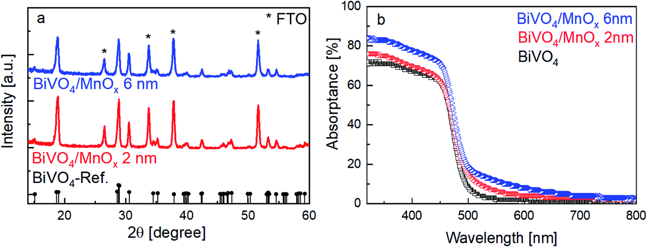 | ||
| Fig. 1 (a) X-ray diffractograms of the BiVO4/MnOx samples with 2 and 6 nm MnOx thickness. In both cases, only peaks belonging to monoclinic BiVO4 (black reference pattern) and FTO substrate are detected. (b) Absorptance of bare BiVO4 and BiVO4/MnOx samples with 2 and 6 nm MnOx thickness. | ||
Fig. 2a shows the current–voltage curves of BiVO4 with different thicknesses of MnOx co-catalysts under 455 nm LED illumination. Up to a MnOx thickness of 4 nm, the photocurrent of the BiVO4 samples at 1 VRHE increases by a factor of ∼3. This photocurrent increase is not due to changes in specific surface area, since the electrochemically active surface area of the BiVO4/MnOx (4 nm) sample is actually ∼25% smaller than that of the bare BiVO4 (Fig. S3†). A small ∼100 mV cathodic shift of the onset potential of BiVO4 can also be observed. Beyond this thickness (i.e., >4 nm), the photocurrent, however, starts to decrease. We confirm the reproducibility of this trend by measuring the photocurrent of at least four samples that were deposited with the same parameters but made in different spray pyrolysis and ALD batches. The production of oxygen from our films was confirmed by performing electrochemical mass spectrometry (EMS) measurements, as shown in Fig. S4†, for the BiVO4/MnOx (4 nm) sample. With a calculated faradaic efficiency of 94 ± 1% at 0.7 VRHE, almost all photocurrent is due to oxygen evolution. A comparison of the photocurrent of these samples with various thicknesses of MnOx co-catalysts at 1 VRHE is shown in Fig. 2b (black curve); the same photocurrent trend as described earlier for the other batch of samples is maintained, which confirms the reproducibility of our samples. To reveal the underlying reason behind the observed trend, we performed intensity modulated photocurrent spectroscopy (IMPS) measurements and determined the charge transfer efficiency (ηCT). The complex IMPS plot at an applied potential of 1 VRHE was evaluated for bare BiVO4 and different thicknesses of MnOx co-catalysts (2, 4, and 6 nm) deposited on BiVO4 films (Fig. S5, ESI†). The resulting charge transfer efficiency, ηCT, for the bare BiVO4 thin films and after addition of MnOx co-catalysts with different thicknesses is plotted in Fig. 2b (red circles); a correlation between ηCT and the photocurrent is clearly present. The obtained charge transfer and surface recombination rate constants (ktr and krec, respectively) are shown in Fig. S6, ESI.† While ktr remains more or less constant with varying thicknesses of the MnOx co-catalyst, krec is minimized at the same optimal thickness of 4 nm. This suggests that the main role of MnOx on BiVO4 is to suppress the surface recombination.
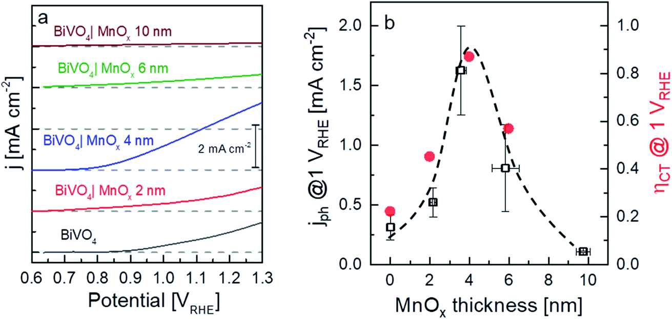 | ||
| Fig. 2 (a) Linear sweep voltammetry (LSV) results of the BiVO4 samples with various thicknesses of MnOx. (b) Current (black squares, average of at least 4 measurements with different sets of samples) and charge transfer efficiency (red circles, calculated from IMPS data) of the BiVO4 samples at 1 VRHE with various thicknesses of MnOx. In all cases, the light source was a 455 nm LED with 20 mW cm−2 power density. The dashed line is added as a guide to the eye. | ||
The photocurrent trend described above cannot be simply explained by the dark electrocatalytic activity trend of the MnOx catalyst. Fig. S7, ESI† shows the current–voltage curves of MnOx films with different thicknesses. The plot shows that increasing the thickness resulted in a monotonous decrease of the current densities. It is therefore clear that MnOx possesses a different role other than improving the catalytic activity when deposited as a co-catalyst on BiVO4. This typical response was also reported by Strandwitz et al.;39 they attributed this to the ohmic loss within the MnOx layers.
In order to elucidate the influence of the MnOx layer on the surface recombination of BiVO4, the chemical nature of the films (and interface) was investigated by XPS. The spectra of the Bi 4f and V 2p core levels are shown in Fig. 3a and b, respectively. With increasing the thickness of the MnOx co-catalyst, it can be clearly seen that the peaks shift towards lower binding energies. In contrast, Fig. 3c shows that the peak position of the Mn 2p core level does not shift with the increasing MnOx thickness. The peak shifts for all these core levels are summarized in Fig. 3d.
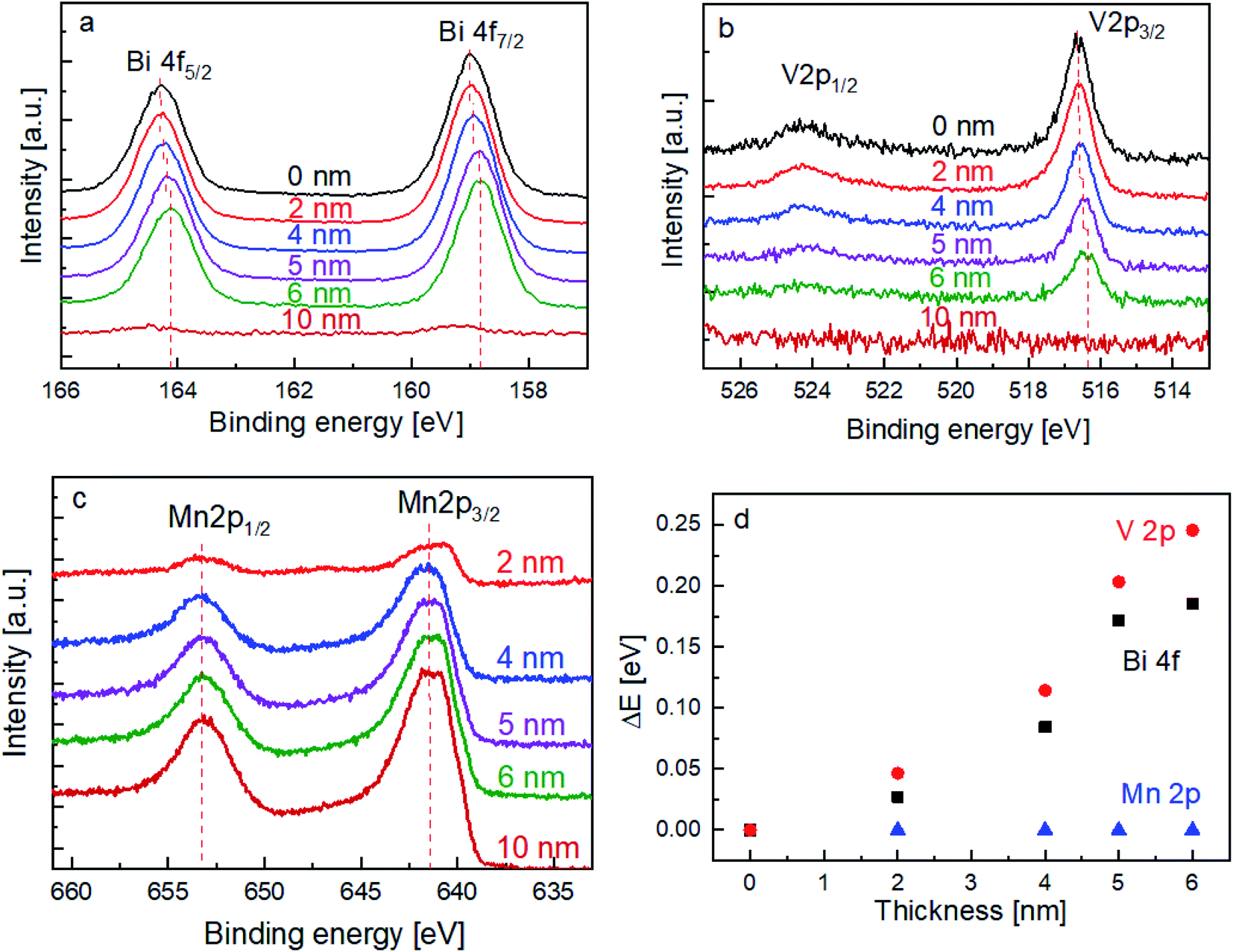 | ||
| Fig. 3 Core level spectra of (a) Bi 4f, (b) V 2p, and (c) Mn 2p for bare BiVO4 and BiVO4 coated with different thicknesses of MnOx (2, 4, 5, 6, and 10 nm). (d) Shift in binding energies (ΔE) for the core levels of Bi 4f, V 2p, and Mn 2p vs. various thicknesses of MnOx. | ||
The above-mentioned observation can be explained by the increase of band bending upon the addition of the MnOx co-catalyst. As illustrated in Scheme 1, with increasing band bending in the BiVO4 film, X-ray excitation with the same photon energy (i.e., 1486.74 eV from our Al Kα radiation) will result in detected photoelectrons with increasing kinetic energy. This translates to a shift of the core level peaks to lower binding energies, which is indeed observed in our experimental results. To further confirm this explanation, we calculated the extent of band bending in our BiVO4 films, assuming the core level peak position values of the BiVO4 single crystal as those of the bulk (159.3 eV for Bi 4f7/2 and 516.9 eV for V 2p3/2).48 The values for BiVO4 films with various MnOx thicknesses are listed in Table S1;† the values calculated using the Bi 4f7/2 peak position agree very well with those calculated using V 2p3/2. Indeed, the extent of band bending increases with the increasing film thickness.
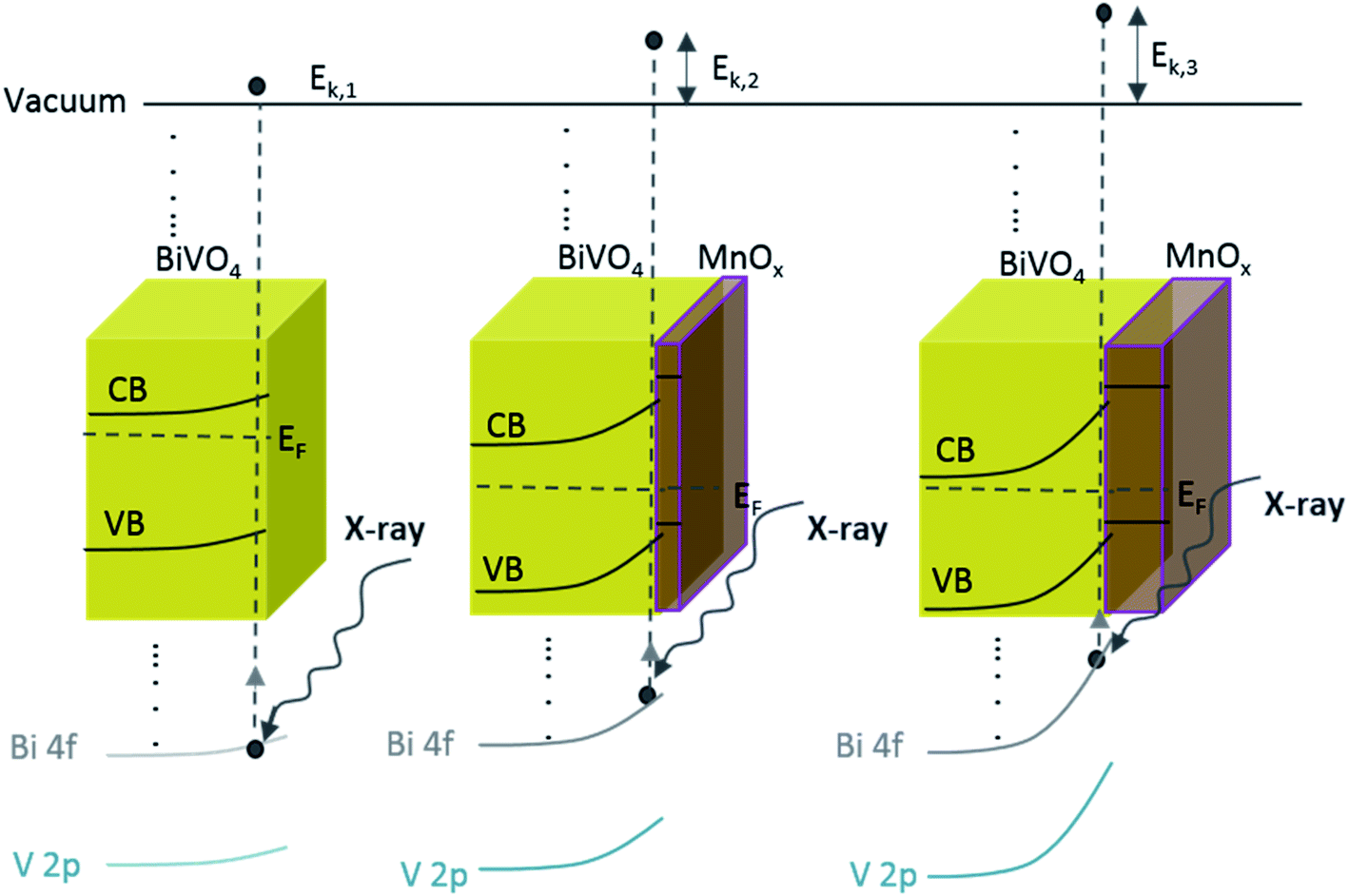 | ||
| Scheme 1 Schematic illustration of the band diagram of BiVO4 and BiVO4 with the increasing MnOx thickness. Since the energy of the X-ray is constant, increasing the band bending at the interface results in photo-emitted electrons with a larger kinetic energy (Ek,1 < Ek,2 < Ek,3). This translates to a shift in the binding energy towards lower values, which explains our observed XPS results (Fig. 3). | ||
The additional band bending explains the improvement of the PEC performance (Fig. 2a) with the increasing thickness of MnOx (up to 4 nm). The increase of band bending has two implications: (i) increase of the space charge width; and (ii) lower surface recombination. The space charge region width can be calculated from eqn (3).
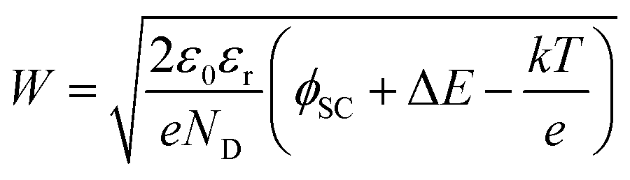 | (3) |
Alternatively, larger band bending may also result in a lower surface majority carrier concentration (nsurf) as shown in the following equation:
 | (4) |
Since surface recombination is a function of nsurf, the overall surface recombination is decreased with decreasing nsurf and the photocurrent is improved. Based on the ∼0.1 eV additional band bending observed for the optimum 4 nm MnOx/BiVO4 sample (see Fig. 3d), we estimate that nsurf is lowered by a factor of ∼40, which is in good agreement with the observed krec decrease from IMPS (Fig. S6, ESI†).
We note that the photocurrent enhancement can also be a result of the surface passivating effect of the MnOx layer, which would also decrease surface recombination. Such an effect has been reported for other overlayers, such as amorphous TiO2, Al2O3 and CoPi.32,50–52 However, while we cannot completely rule out this explanation, the good quantitative agreement between the decrease of krec and nsurf in our films suggests that surface passivation does not play a major role.
Although the above-mentioned band bending observation can satisfactorily explain the increase of the photocurrent of BiVO4 after deposition of MnOx films, it cannot account for the overall photocurrent trend; the band bending continues to increase with the increasing MnOx thickness, yet the photocurrent decreases when the MnOx films are thicker than 4 nm. A competing mechanism therefore exists, which compensates for the increasing band bending at the BiVO4/MnOx interface. One possibility is simply the lower (dark) electrochemical activity of MnOx with the increasing thicknesses (Fig. S7, ESI†), which has been shown to be related to the poor conductivity of the MnOx layer.39 To confirm if this is also the case when MnOx is deposited on BiVO4, electrochemical impedance spectroscopy (EIS) was conducted for BiVO4 samples with different thicknesses of MnOx. We focus on two thicknesses of the MnOx layer on BiVO4: 4 nm as the optimum thickness and 6 nm as the thickness at which a decrease in photocurrent already occurs. The Nyquist plot for the BiVO4 coated with 4 nm of MnOx is shown in Fig. S8a.† Two semicircles can be clearly observed. We apply a resistance-based analysis method on the resistances in the films, as recently established by Moehl et al. for multilayer water splitting photocathodes.53 In order to assign the identity of each semicircle, the measurements were also conducted at different applied potentials. As shown in Fig. S8a,† increasing the potential does not change the first semicircle, but a systematic decrease of the radius of the second semicircle can be observed. We therefore, attributed the first semicircle to the resistance of the MnOx layer (RMnOx) and the second semicircle to the charge transfer resistance (Rct). Fig. S8b† shows the Nyquist plot of the BiVO4 films with 4 and 6 nm of MnOx measured at ∼1.23 VRHE. Rct decreases with the increasing MnOx thickness, while RMnOx remains relatively constant (62.3 ± 9.3 vs. 64 ± 14 Ω for the 4 and 6 nm MnOx films, respectively). These results therefore cannot explain the decrease of photocurrent for BiVO4 with MnOx films thicker than 4 nm.
Another plausible explanation for the decrease of photocurrent beyond 4 nm thickness of MnOx is the presence of shunting pathways. For example, Boettcher and co-workers showed that in the case of NiFeOx co-catalysts on a hematite photoanode, direct contact between NiFeOx and the underlying FTO substrate—due to the porosity or the existence of pinholes in the hematite photoanode—provides a pathway for electron–hole recombination (i.e., shunting).13 To determine whether this may be the case for our films, dark cyclic voltammetry measurements were performed for FTO and bare BiVO4 in 50 mM ferri/ferrocyanide with 0.1 M supporting KCl electrolyte (Fig. 4a). The dark current for the FTO shows clear peaks corresponding to the oxidation and reduction of the [Fe(CN)6]3−/[Fe(CN)6]4 redox couple. For a dense BiVO4 film (i.e., no pinholes and the FTO is therefore not exposed to the electrolyte), these redox peaks should not be visible and only negligible dark currents are measured.13 However, the same dark cyclic voltammetry measurements on our BiVO4 film show the [Fe(CN)6]3−/[Fe(CN)6]4 redox peaks, albeit being smaller and shifted to higher/lower potentials. This suggests that pinholes are indeed present on our spray-pyrolysed BiVO4. For the MnOx/BiVO4 samples, these pinholes represent the area where direct contact between MnOx and FTO can occur. In addition, we measured the dark current for the BiVO4 samples with different thicknesses of MnOx in 0.1 M KPi electrolyte. Indeed, the dark current increases for samples with MnOx films thicker than 4 nm (Fig. 4b), confirming the presence of MnOx/FTO contact. These observations, therefore, suggest that a shunting effect is the reason behind the decreasing photocurrent for thicker MnOx films.
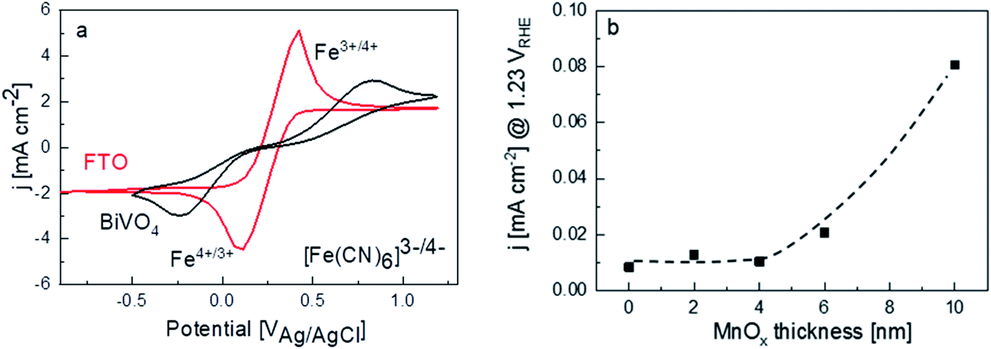 | ||
| Fig. 4 (a) Voltammograms of FTO and bare BiVO4 in 0.1 M KCl and 50 mM (Fe(CN)6)3−/4− at the 10 mV s−1 scan rate. (b) Dark current measurements in 0.1 M KPi for bare BiVO4 films and 2, 4, 6, and 10 nm MnOx coated BiVO4. The dashed line is added as a guide to the eye. | ||
The presence of the pinholes, and therefore the shunting pathways, is further confirmed with additional microscopy measurements. The scanning helium ion microscopy top view image of the BiVO4 film shows that it is not fully compact, i.e., some parts of the FTO substrate are not covered (Fig. 5). Fig. 6 shows the scanning transmission electron microscopy (STEM) cross-section image of a BiVO4 sample with 10 nm-thick MnOx layers. The EDX-STEM mapping (Fig. 6b–f) shows the pinholes on BiVO4 quite clearly. From the composite map (Fig. 6f), the areas in which MnOx is in direct contact with FTO are marked with the red arrows.
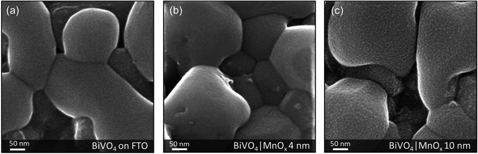 | ||
| Fig. 5 Helium ion microscopy (HIM) image of (a) BiVO4 on FTO, (b) BiVO4 decorated with 4 nm MnOx, and (c) BiVO4 decorated with 10 nm MnOx. | ||
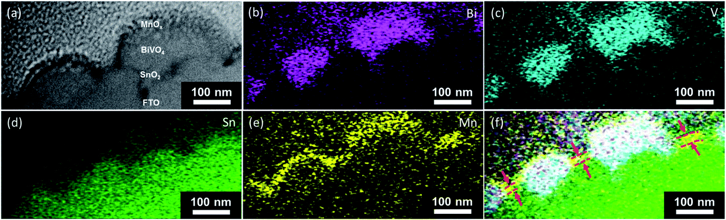 | ||
| Fig. 6 (a) A cross-section view of the morphology of the BiVO4 films coated with MnOx. Elemental distribution (net counts, individual intensity scaling) of (b) Bi, (c) V, (d) Sn, (e) Mn, and (f) composite signals as obtained by energy dispersive X-ray spectrometry for MnOx modified BiVO4. | ||
We can now summarize our findings on the role of MnOx films on BiVO4 and the correlation with the observed photocurrent trend. The deposition of MnOx co-catalysts on BiVO4 films with increasing MnOx thickness results in additional band bending at the interface. This leads to lower surface majority carrier concentration, reduced surface recombination, and higher photocurrent. When the films become too thick, they can make direct contact with the underlying FTO. This causes a shunt between the surface of the BiVO4 and the FTO substrate that causes recombination. These two competing effects (illustrated in Scheme 2) explain the photocurrent being maximized for the BiVO4 films with 4 nm MnOx co-catalysts.
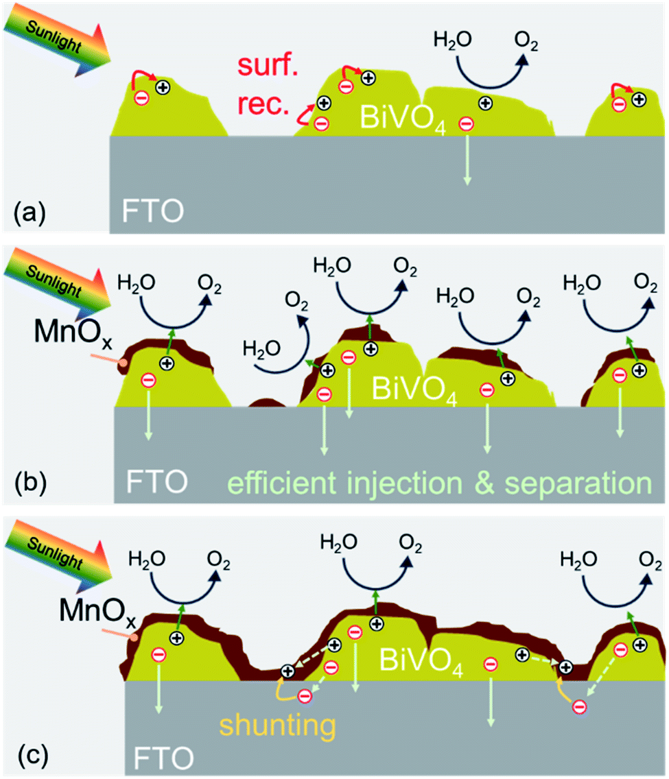 | ||
| Scheme 2 (a) In bare BiVO4, charge transfer from the surface of BiVO4 is limited by surface recombination (red arrows). (b) When a thin MnOx film is deposited on the surface of BiVO4 (up to 4 nm), a discontinuous layer is formed. At the interface, the band bending is enhanced, and the surface recombination is suppressed. (c) Depositing a thicker MnOx film (>4 nm) leads to a full coverage, even at the exposed FTO surface. Direct contact between MnOx and FTO results in shunting pathways. | ||
Conclusions
In summary, we have investigated the role of ultra-thin ALD MnOx co-catalyst layers on BiVO4 photoanodes. Upon the deposition of MnOx, the PEC performance of BiVO4 is enhanced. The photocurrent reaches its maximum for a MnOx thickness of 4 nm (∼3-fold improvement as compared to the bare BiVO4); beyond this thickness the photocurrent decreases. We showed that the MnOx dark catalytic activity and conductivity trends cannot explain this photocurrent trend. IMPS analysis showed that the charge transfer efficiency and surface recombination rate constant follow the same trend with MnOx thickness as the photocurrent. We found that MnOx introduces additional band bending (up to ∼0.2 eV) at the BiVO4/MnOx interface, as shown from the XPS analysis, which reduces surface recombination. However, at the same time, due to the morphological nature of our spray-pyrolysed BiVO4 films, increasing the MnOx thickness also increases the possibility of MnOx filling the pinholes and creating direct contact with the underlying FTO substrate. We showed that this is indeed the case using electrochemical and TEM analysis. This results in shunting, which increases the electron–hole recombination and cancels out the favorable effect of band bending for thicker MnOx films. Overall, this study sheds light on the main role of MnOx co-catalysts on BiVO4 and the underlying reason behind the co-catalyst thickness optimization. It is expected that the phenomena observed in our system can be extended to other semiconductors and co-catalysts, especially those with a similar morphology.Conflicts of interest
There are no conflicts to declare.Acknowledgements
This research was supported by the German Federal Ministry of Education and Research (BMBF), project “MANGAN” (03SF0505). We gratefully acknowledge Holger Kropf for the assistance with TEM sample preparation, Prince Saurabh Bassi for discussions, and Yasemin Atasay for her help in the reproducibility experiments. The helium ion and transmission electron microscopy studies were performed in the Corelab Correlative Microscopy and Spectroscopy at Helmholtz-Zentrum Berlin.References
- M. G. Walter, E. L. Warren, J. R. McKone, S. W. Boettcher, Q. Mi, E. A. Santori and N. S. Lewis, Chem. Rev., 2010, 110, 6446–6473 CrossRef CAS PubMed.
- A. J. Bard and M. A. Fox, Acc. Chem. Res., 1995, 28, 141–145 CrossRef CAS.
- Y. Tachibana, L. Vayssieres and J. R. Durrant, Nat. Photonics, 2012, 6, 511 CrossRef CAS.
- M. T. M. Koper, J. Electroanal. Chem., 2011, 660, 254–260 CrossRef CAS.
- Gurudayal, L. M. Peter, L. H. Wong and F. F. Abdi, ACS Appl. Mater. Interfaces, 2017, 9, 41265–41272 CrossRef CAS PubMed.
- J. A. Seabold and K.-S. Choi, J. Am. Chem. Soc., 2012, 134, 2186–2192 CrossRef CAS PubMed.
- Y. Ma, S. R. Pendlebury, A. Reynal, F. Le Formal and J. R. Durrant, Chem. Sci., 2014, 5, 2964–2973 RSC.
- A. Song, P. Plate, A. Chemseddine, F. Wang, F. F. Abdi, M. Wollgarten, R. van de Krol and S. P. Berglund, J. Mater. Chem. A, 2019, 7, 9183–9194 RSC.
- Y. Park, K. J. McDonald and K.-S. Choi, Chem. Soc. Rev., 2013, 42, 2321–2337 RSC.
- T. W. Kim and K.-S. Choi, Science, 2014, 343, 990–994 CrossRef CAS PubMed.
- A. Ghosh, N. Kumari and A. Bhattacharjee, Pramana, 2015, 84, 621–635 CrossRef CAS.
- L. Trotochaud, S. L. Young, J. K. Ranney and S. W. Boettcher, J. Am. Chem. Soc., 2014, 136, 6744–6753 CrossRef CAS PubMed.
- J. Qiu, H. Hajibabaei, M. R. Nellist, F. A. L. Laskowski, S. Z. Oener, T. W. Hamann and S. W. Boettcher, ACS Energy Lett., 2018, 3, 961–969 CrossRef CAS.
- D. K. Zhong, S. Choi and D. R. Gamelin, J. Am. Chem. Soc., 2011, 133, 18370–18377 CrossRef CAS PubMed.
- M. Kölbach, S. Fiechter, R. van de Krol and P. Bogdanoff, Catal. Today, 2017, 290, 2–9 CrossRef.
- T. Higashi, H. Nishiyama, Y. Suzuki, Y. Sasaki, T. Hisatomi, M. Katayama, T. Minegishi, K. Seki, T. Yamada and K. Domen, Angew. Chem., Int. Ed., 2019, 58, 2300–2304 CrossRef CAS PubMed.
- M. Barroso, C. A. Mesa, S. R. Pendlebury, A. J. Cowan, T. Hisatomi, K. Sivula, M. Gratzel, D. R. Klug and J. R. Durrant, Proc. Natl. Acad. Sci. U. S. A., 2012, 109, 15640–15645 CrossRef CAS PubMed.
- Y.-R. Hong, Z. Liu, S. F. B. S. A. Al-Bukhari, C. J. J. Lee, D. L. Yung, D. Chi and T. S. A. Hor, Chem. Commun., 2011, 47, 10653–10655 RSC.
- C. Y. Cummings, F. Marken, L. M. Peter, A. A. Tahir and K. G. U. Wijayantha, Chem. Commun., 2012, 48, 2027–2029 RSC.
- P. S. Bassi, R. P. Antony, P. P. Boix, Y. Fang, J. Barber and L. H. Wong, Nano Energy, 2016, 22, 310–318 CrossRef CAS.
- J. A. Seabold and K.-S. Choi, Chem. Mater., 2011, 23, 1105–1112 CrossRef CAS.
- M. Higashi, K. Domen and R. Abe, J. Am. Chem. Soc., 2012, 134, 6968–6971 CrossRef CAS PubMed.
- F. F. Abdi, L. Han, A. H. M. Smets, M. Zeman, B. Dam and R. van de Krol, Nat. Commun., 2013, 4, 2195 CrossRef PubMed.
- H. Ye, H. S. Park and A. J. Bard, J. Phys. Chem. C, 2011, 115, 12464–12470 CrossRef CAS.
- J. Deng, M. R. Nellist, M. B. Stevens, C. Dette, Y. Wang and S. W. Boettcher, Nano Lett., 2017, 17, 6922–6926 CrossRef CAS PubMed.
- M. Kim, B. Lee, H. Ju, J. Y. Kim, J. Kim and S. W. Lee, Adv. Mater., 2019, 31, 1903316 CrossRef PubMed.
- S. D. Tilley, M. Schreier, J. Azevedo, M. Stefik and M. Graetzel, Adv. Funct. Mater., 2014, 24, 303–311 CrossRef CAS.
- F. F. Abdi and R. van de Krol, J. Phys. Chem. C, 2012, 116, 9398–9404 CrossRef CAS.
- M. Chen, Y. Liu, C. Li, A. Li, X. Chang, W. Liu, Y. Sun, T. Wang and J. Gong, Energy Environ. Sci., 2018, 11, 2025–2034 RSC.
- D. R. Gamelin, Nat. Chem., 2012, 4, 965–967 CrossRef CAS PubMed.
- Y. Ma, A. Kafizas, S. R. Pendlebury, F. Le Formal and J. R. Durrant, Adv. Funct. Mater., 2016, 26, 4951–4960 CrossRef CAS.
- C. Zachäus, F. F. Abdi, L. M. Peter and R. van de Krol, Chem. Sci., 2017, 8, 3712–3719 RSC.
- M. R. Nellist, J. Qiu, F. A. L. Laskowski, F. M. Toma and S. W. Boettcher, ACS Energy Lett., 2018, 3, 2286–2291 CrossRef CAS.
- L. Han, F. F. Abdi, R. van de Krol, R. Liu, Z. Huang, H.-J. Lewerenz, B. Dam, M. Zeman and A. H. M. Smets, ChemSusChem, 2014, 7, 2832–2838 CrossRef CAS PubMed.
- J.-W. Jang, D. Friedrich, S. Müller, M. Lamers, H. Hempel, S. Lardhi, Z. Cao, M. Harb, L. Cavallo, R. Heller, R. Eichberger, R. van de Krol and F. F. Abdi, Adv. Energy Mater., 2017, 7, 1701536–1701546 CrossRef.
- F. F. Abdi and S. P. Berglund, J. Phys. D: Appl. Phys., 2017, 50, 193002–1930023 CrossRef.
- I. Y. Ahmet, Y. Ma, J.-W. Jang, T. Henschel, B. Stannowski, T. Lopes, A. Vilanova, A. Mendes, F. F. Abdi and R. van de Krol, Sustainable Energy Fuels, 2019, 3, 2366–2379 RSC.
- X. Du, T. Zhao, Z. Xiu, Z. Yang, Z. Xing, Z. Li, S. Yang and W. Zhou, J. Hazard. Mater., 2019, 377, 330–340 CrossRef CAS PubMed.
- N. C. Strandwitz, D. J. Comstock, R. L. Grimm, A. C. Nichols-Nielander, J. Elam and N. S. Lewis, J. Phys. Chem. C, 2013, 117, 4931–4936 CrossRef CAS.
- M. Lamers, W. Li, M. Favaro, D. E. Starr, D. Friedrich, S. Lardhi, L. Cavallo, M. Harb, R. van de Krol, L. H. Wong and F. F. Abdi, Chem. Mater., 2018, 30, 8630–8638 CrossRef CAS.
- M. Lamers, S. Fiechter, D. Friedrich, F. F. Abdi and R. van de Krol, J. Mater. Chem. A, 2018, 6, 18694–18700 RSC.
- F. F. Abdi and R. van de Krol, J. Phys. Chem. C, 2012, 116, 9398–9404 CrossRef CAS.
- Y. Liang, T. Tsubota, L. P. A. Mooij and R. van de Krol, J. Phys. Chem. C, 2011, 115, 17594–17598 CrossRef CAS.
- A. C. Bronneberg, C. Höhn and R. van de Krol, J. Phys. Chem. C, 2017, 121, 5531–5538 CrossRef CAS.
- E. Langereis, S. B. S. Heil, H. C. M. Knoops, W. Keuning, M. C. M. van de Sanden and W. M. M. Kessels, In situ spectroscopic ellipsometry as a versatile tool for studying atomic layer deposition, J. Phys. D: Appl. Phys., 2009, 42, 073001–073019 CrossRef.
- R. van de Krol and M. Grätzel, Photoelectrochemical Hydrogen Production, Springer, 2012 Search PubMed.
- L. M. Peter, E. A. Ponomarev and D. J. Fermín, J. Electroanal. Chem., 1997, 427, 79–96 CrossRef CAS.
- M. Favaro, R. Uecker, S. Nappini, I. Píš, E. Magnano, H. Bluhm, R. van de Krol and D. E. Starr, J. Phys. Chem. C, 2019, 123, 8347–8359 CrossRef CAS.
- W. W. Gärtner, Phys. Rev., 1959, 116, 84–87 CrossRef.
- D. Eisenberg, H. S. Ahn and A. J. Bard, J. Am. Chem. Soc., 2014, 136, 14011–14014 CrossRef CAS PubMed.
- M. G. Ahmed, I. E. Kretschmer, T. A. Kandiel, A. Y. Ahmed, F. A. Rashwan and D. W. Bahnemann, ACS Appl. Mater. Interfaces, 2015, 7, 24053–24062 CrossRef CAS PubMed.
- A. Kafizas, X. Xing, S. Selim, C. A. Mesa, Y. Ma, C. Burgess, M. A. McLachlan and J. R. Durrant, Catal. Today, 2019, 321–322, 59–66 CrossRef CAS.
- T. Moehl, W. Cui, R. Wick-Joliat and S. D. Tilley, Sustainable Energy Fuels, 2019, 3, 2067–2075 RSC.
Footnote |
| † Electronic supplementary information (ESI) available. See DOI: 10.1039/d0ta00939c |
| This journal is © The Royal Society of Chemistry 2020 |