
Mixed-dimensional PdSe2/SiNWA heterostructure based photovoltaic detectors for self-driven, broadband photodetection, infrared imaging and humidity sensing†
Di
Wu
 a,
Cheng
Jia
a,
Fenghua
Shi
b,
Longhui
Zeng
*c,
Pei
Lin
a,
Lin
Dong
a,
Zhifeng
Shi
a,
Yongtao
Tian
a,
Xinjian
Li
a and
Jiansheng
Jie
*d
a,
Cheng
Jia
a,
Fenghua
Shi
b,
Longhui
Zeng
*c,
Pei
Lin
a,
Lin
Dong
a,
Zhifeng
Shi
a,
Yongtao
Tian
a,
Xinjian
Li
a and
Jiansheng
Jie
*d
aSchool of Physics and Microelectronics, Key Laboratory of Material Physics, Ministry of Education, Zhengzhou University, Zhengzhou, Henan 450052, China
bCollege of Physics and Electronic Information, Anhui Normal University, Wuhu, Anhui 241000, China
cDepartment of Applied Physics and Materials Research Center, The Hong Kong Polytechnic University, Hung Hom, Kowloon, Hong Kong, China. E-mail: lhzeng.hfut@gmail.com
dInstitute of Functional Nano & Soft Materials (FUNSOM), Soochow University, Suzhou, Jiangsu 215123, China. E-mail: jsjie@suda.edu.cn
First published on 9th January 2020
Abstract
The new discovery of two-dimensional (2D) palladium diselenide (PdSe2) films has attracted intensive research interest due to their unique asymmetric crystal structure and extraordinary optoelectronic properties, showing great potential for broadband and polarization photodetection. Herein, we have developed for the first time a self-driven, highly polarization-sensitive, broadband photovoltaic detector based on a PdSe2/Si nanowire array (SiNWA) heterostructure. Owing to the strong light confinement effect of the SiNWA and broadband light absorption of PdSe2, the present device exhibits pronounced photovoltaic behavior and excellent performance in terms of a high responsivity of 726 mA W−1, a large specific detectivity of 3.19 × 10¹⁴ Jones, an ultrabroad spectrum response range of 0.2–4.6 μm, and a fast response speed to monitor nanosecond pulsed light signals. Significantly, an impressive polarization sensitivity of 75 is achieved for the heterostructure device, which is among the highest for 2D material-based photodetectors. Thanks to the outstanding imaging capability, the detector can record images in both near infrared (NIR) and mid-infrared (MIR) ranges with a decent resolution. Moreover, the device exhibits light-enhanced humidity sensing behavior with a high sensitivity and a fast response/recovery time. Given these remarkable device features, the PdSe2/SiNWA heterostructure will hold great promise for high-performance, polarization-sensitive broadband photodetection, infrared imaging and humidity sensing applications.
Introduction
As the first discovered two-dimensional (2D) layered material, graphene has attracted tremendous interest due to its outstanding electrical, optical, and mechanical properties.1 Graphene has found exciting applications in a variety of fields, such as electronics, biosensors, solar cells, and photocatalysts.2–6 Despite the enormous progress, the wide application of graphene in optoelectronic devices is still impeded by disadvantages such as its gapless nature, weak light absorption, and short photocarrier lifetime.7,8 Such predicaments are a key driving force for the research community towards the exploration of other promising and alternative 2D layered materials to overcome the above shortcomings of graphene. Recently, graphene-analogous 2D materials such as arsenene,9 black phosphorus,10 antimonene,11 silicone,12 and layered transition metal dichalcogenides (TMDs, MoS2, WS2, WSe2, and MoSe2) with exotic properties have come under the spotlight.13–19 Also, various synthetic methods such as mechanically assisted exfoliation,20 liquid phase exfoliation,21,22 molecular beam epitaxy,23 chemical vapor deposition (CVD),24 and vapor phase deposition have been employed to produce 2D layered materials. These 2D layered materials display high carrier mobility, strong light–matter interaction, and excellent mechanical flexibility.25 Such distinctive materials properties, along with the layer-dependent bandgap, make them attractive and promising candidates for high-performance optoelectronic devices.26,27Besides the above introduced 2D layered materials, palladium diselenide (PdSe2), the newly studied group-10 noble metal dichalcogenide with a unique anisotropic structure, has demonstrated excellent optical and electrical properties such as good air stability, a high carrier mobility, and a wide tunable bandgap from 0 eV (bulk) to 1.3 eV (monolayer). These characteristics endow PdSe2 with the capability to construct highly polarization-sensitive, air-stable and broadband photodetectors.28–31 However, only a few studies regarding related properties of PdSe2 and PdSe2-based devices have been reported thus far. For instance, Li et al. achieved the deposition of bilayer PdSe2 islands on graphene using molecular beam epitaxy (MBE) and systemically studied their optoelectronic properties.32 Besides, Liu et al. fabricated a phototransistor based on few-layer PdSe2 films that were mechanically exfoliated from the bulk form, showing a high mobility of 216 cm2 V−1 s−1 dominated by electron transport behavior.33 Recently, Zhang et al. developed high-performance photoconductors based on 2D PdSe2 flakes, revealing an impressive responsivity of 708 A W−1 and an EQE of 82![[thin space (1/6-em)]](https://www.rsc.org/images/entities/char_2009.gif) 700% under 1064 nm illumination.34
700% under 1064 nm illumination.34
Meanwhile, the surfaces of 2D materials are free of dangling bonds, which enables them to be easily integrated with other semiconductor materials of different dimensionality, resulting in high-quality mixed-dimensional van der Waals (vdW) heterostructures.35 The construction of mixed-dimensional vdW heterostructures has several advantages: (i) great light absorption compared with all-2D vdW heterostructures.13 (ii) More availability of component materials and a broader range of spectral selectivity ranging from UV to IR.36–38 (iii) The presence of a built-in electric field in the heterojunction can effectively accelerate the separation and transport of photo-generated carriers, leading to a fast response speed.39 (iv) More powerful and extra functions compared with the individual component-based devices. For instance, a heterojunction photodetector with a photovoltaic effect can be operated at zero bias (self-driven) to maximize the signal–noise ratio (SNR).40 Therefore, the construction of the mixed-dimensional vdW heterostructures is beneficial to further improve the performance of photodetectors. On the other hand, as one of the most important semiconductor materials, silicon (Si) has been widely applied in electronic and optoelectronic devices.41–43 Si nanostructures, such as Si nanowire arrays (SiNWAs), have received intensive attention in recent years due to their enhanced light absorption and excellent electron transport characteristics.13,44 In addition, enhanced device performances have been achieved in photodetectors by using SiNWAs as the light harvesting medium.45 With these distinct properties, it is expected that the construction of a 2D PdSe2/SiNWA heterojunction device may lead to a high-performance broadband photodetector.
Herein, we demonstrate, for the first time, a self-driven, polarization-sensitive, broadband photovoltaic detector by directly transferring 2D PdSe2 onto the top surfaces of vertically standing one-dimensional (1D) Si nanowire arrays (SiNWA). By taking advantage of the strong light confinement effect, the high-quality PdSe2/SiNWA mixed-dimensional vdW heterostructure shows apparent photovoltaic behavior under light illumination, enabling the device to work without an external power supply. Also, due to the strong infrared light absorption of multilayer PdSe2 films, the present photovoltaic detector is capable of detecting a broadband spectrum from 200 nm to 4.6 μm. Impressive device parameters in terms of a high responsivity of 726 mA W−1, a large specific detectivity of 3.19 × 10¹⁴ Jones, a fast response speed of 25.1/34 μs, and a high polarization sensitivity of 75 are attained. Significantly, the PdSe2/SiNWA heterostructure-based photovoltaic detector can serve as a near infrared (NIR)/mid-infrared (MIR) image sensor with a well-pleasing spatial resolution. Moreover, thanks to the large surface-to-volume ratio of the PdSe2 film and SiNWA, the heterostructure device is very sensitive to relative humidity (RH), and the light-enhanced humidity sensing properties are explored. Given these superior device characteristics, PdSe2/SiNWA mixed-dimensional vdW heterostructure devices may find great potential application in optoelectronic systems and devices.
Experimental details
Synthesis and characterization of 2D PdSe2 films and SiNWA
2D PdSe2 films were obtained by a simple selenization method.28 In detail, a Pd metal layer was prepared on a SiO2/Si substrate using a magnetron sputtering system. Then, the as-deposited Pd film was placed at the center zone of a tube furnace, and high-purity selenium powder (99.99%) was put in the upstream zone. The selenium powder was heated to 240 °C, and the center of the tube furnace was heated up to 480 °C for 90 min with an Ar/H2 (95/5 sccm) gas mixture. The SiNWA was synthesized via a Ag-assisted chemical etching method.44 The morphologies of PdSe2 and SiNWA were recorded by field-emission scanning electron microscopy (FESEM, JEOL, JSM-6700F) equipped with energy dispersive spectroscopy (EDS, Oxford instruments). In addition, the as-synthesized large-area PdSe2 films were characterized by using a Raman spectrometer (Horiba, LabRAM HR Evolution), an atomic force microscope (AFM, VeecoNanoscope V), an X-ray photoelectron spectrometer (XPS, Thermo ESCALAB 250) and a UV-Vis-NIR spectrophotometer (Hitachi, UH4150).Device fabrication and characterization
To fabricate the PdSe2/SiNWA heterostructure device, the 2D PdSe2 film was transferred onto the top of the SiNWA through a polymethyl methacrylate (PMMA)-assisted process. Afterwards, a Au electrode (100 nm) was deposited on the PdSe2 film as an ohmic contact to the film, and an In/Ga alloy was pasted onto the rear side of the Si substrate as the ohmic contact. The optoelectrical performances of the device were evaluated using a semiconductor parameter analyzer system (Keithley 4200-SCS, Tektronix), monochromator (Omni-λ300, Zolix Instruments), lock-in amplifier (SR830, Stanford Research System), function generator (SDG1032X, Siglent) and an oscilloscope (DPO2012B, Tektronix) at ∼20% relative humidity (RH). During photoresponse measurements, a Xe lamp (Gloria-X150A, Zolix Instruments) and lasers with different wavelengths (265 nm, 980 nm, 2.2 μm, 3 μm, and 4.6 μm) were used as light sources. For the humidity sensing study, supersaturated aqueous solutions of LiCl, MgCl2, Mg(NO3)2, NaCl, KCl, and KNO3 were used to provide 11, 33, 54, 75, 85 and 95% RH at room temperature, respectively.Theoretical calculations
The electric field energy density distribution of the device was simulated by the FDTD method. The refractive index of c-silicon reported by Palik was used.46 Due to the large difference in both the real and imaginary part of the c-silicon refractive index over the wavelength range from 200–2000 nm, it is very difficult to fit the optical index in the whole range in a single simulation. So the simulations were divided into two regions for better fitting with a smaller fitting error (200–800 nm and 800–2000 nm). To reduce the memory requirements of a simulation, the thickness of bulk silicon is set as 50 μm, much less than that of a real silicon wafer. As a result, the obtained simulated absorption spectra have notable differences compared to the experimental results around the absorption edge. For SiNWA simulation, according to the NW diameter distribution shown in Fig. 1h, the final absorption spectrum of the SiNWA was obtained by averaging the results of NWs with diameters of 100 nm, 120 nm, 140 nm, 160 nm, 180 nm, and 200 nm with a period of 80 nm.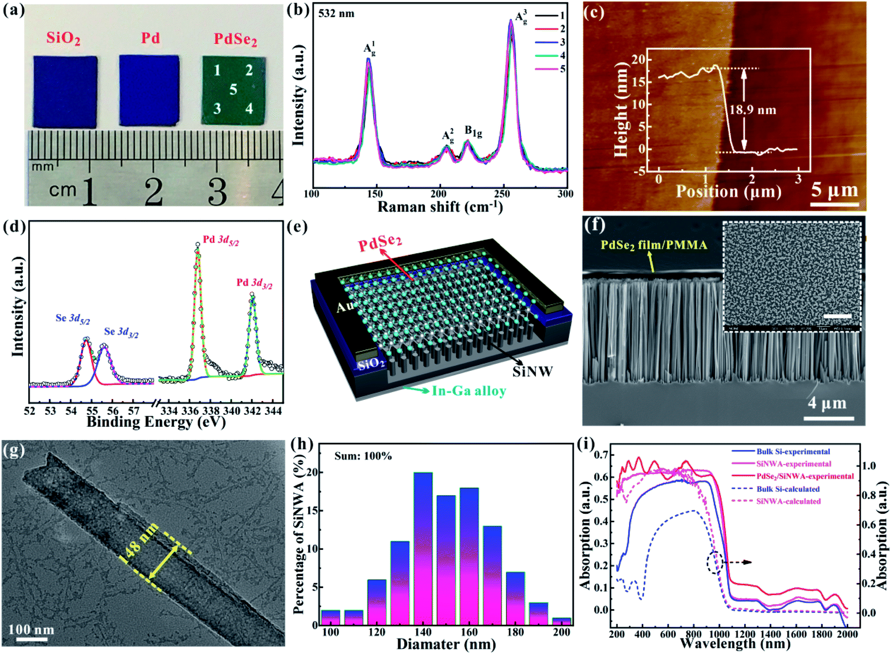 | ||
| Fig. 1 (a) Photograph of the PdSe2 film fabricated on the SiO2/Si substrate. (b) Raman spectra of the 2D PdSe2 film acquired from different points marked in (a). (c) AFM image of the PdSe2 film with the height profile. (d) XPS spectra of the PdSe2 film, showing the binding energies of Pd 3d and Se 3d peaks. (e) Schematic diagram of the PdSe2/SiNWA mixed-dimensional vdW heterostructure device. (f) Cross-sectional SEM image of the PdSe2/SiNWA heterostructure. The inset shows the top-view image of the heterostructure. The scale bar in the inset is 20 μm. (g) TEM image of a single SiNW. (h) Statistical distribution of the diameters of SiNWs. (i) Absorption spectra of the SiNWA, bulk Si and PdSe2/SiNWA heterostructure (solid line). The theoretically calculated absorption spectra of the bulk Si and SiNWA are also demonstrated (dashed line). | ||
Results and discussion
In this work, large-area PdSe2 films were grown by a straightforward selenization process on SiO2/Si substrates at a relatively low temperature. After the transformation of the precursor Pd layer into 2D layered PdSe2, an obvious color change from blue to dark green can be observed, as shown in Fig. 1a. With the availability of large-area and continuous PdSe2 films, the sample was further characterized by Raman spectroscopy. In Fig. 1b, Raman spectra acquired from five randomly selected positions in Fig. 1a show four obvious peaks at ∼144 cm−1, ∼205 cm−1, ∼222 cm−1, and ∼256 cm−1 due to A1g, A2g, and B1g active modes and A3g vibration mode with excellent consistency, suggesting the good uniformity and homogeneity of the large-area 2D PdSe2 films. Fig. 1c shows an AFM image of the PdSe2 film, revealing a multilayer structure of the as-synthesized PdSe2 film with a thickness of ∼18.9 nm. In addition, the chemical composition of the as-grown PdSe2 film was further confirmed by XPS characterization. Fig. 1d shows the typical deconvoluted XPS results for Pd 3d and Se 3d of the PdSe2 film. The Pd 3d can be deconvoluted into two peaks at 336.8 and 342 eV assigned to Pd 3d5/2 and Pd 3d3/2, respectively. The Se 3d can be deconvoluted into two peaks at 54.8 and 55.6 eV, which correspond to Se 3d5/2 and Se 3d3/2 orbitals, respectively. By quantifying the peaks, the atomic ratio of Pd/Se was determined to be ∼1:2. Furthermore, the FESEM image of the PdSe2 film on the Si substrate indicates that the film is continuous and uniform with a smooth surface (Fig. S1a†). Elemental mapping in a randomly selected area also demonstrates that both Pd and Se elements are uniformly distributed over the observed zone (Fig. S1b and c†).
Fig. 1e shows the schematic diagram of the photovoltaic detector based on the PdSe2/SiNWA mixed-dimensional vdW heterostructure. The detailed fabrication process and the photograph of an assembled device could be found in Fig. S2 and S3,† respectively. From the cross-sectional SEM image of the PdSe2/SiNWA heterostructure device (Fig. 1f), we note that the PdSe2 film was fully supported by the vertically aligned SiNWA. The length of the SiNW is about 8 μm, while the diameter of a representative Si nanowire (NW) is ∼148 nm (Fig. 1g). According to the statistical distribution shown in Fig. 1h, the diameter of the NWs is determined to be in the range of 100–200 nm, with an average value of ∼150 nm. Furthermore, we systemically compared the absorption spectra of the bulk Si, the SiNWA and the PdSe2/SiNWA hybrid system. Note that the SiNWA displays enhanced light absorption in the entire region compared to the bulk Si, which is consistent with the theoretical calculation based on finite-difference time domain (FDTD) simulations. More importantly, by depositing the 2D PdSe2 film on the top surface of the SiNWA, the light absorption of the PdSe2/SiNWA hybrid system is further enhanced and extended beyond 1100 nm due to the broadband absorption of the 2D PdSe2 film.
Fig. 2a presents the current–voltage (I–V) curves of the PdSe2/SiNWA heterostructure measured in the dark (black curves) and under light illumination (colored curves). Notably, a remarkable current rectifying characteristic with a rectification ratio of over 102 within ±5 V was observed, revealing the high-quality of the PdSe2/SiNWA heterostructure. Au and In/Ga alloys were used as the electrodes in the device, which showed good ohmic contacts with PdSe2 and Si, respectively (Fig. S4†). Hence, the diode characteristics of the device could be attributed to the formation of a junction at the PdSe2/SiNWA interface. Once the device was illuminated using light signals, obvious photoresponse behavior was observed in the reverse bias direction. Careful examination also revealed that the device displayed pronounced photovoltaic behavior in a wide wavelength range, making the present device a broadband and self-driven photovoltaic detector. Fig. 2b presents the time-resolved photoresponse of the PdSe2/SiNWA heterostructure photovoltaic detector at zero bias in a broad spectrum ranging from deep ultraviolet (DUV) to MIR. The photovoltaic detector shows stable, repeatable and fast response to incident light with current on/off ratios (Ion/Ioff) of 104 for 265 nm (2.1 mW cm−2), 106 for 980 nm (56.6 mW cm−2), 102 for 2.2 μm (150 mW cm−2) and 3 μm (35.9 mW cm−2), and 26 for 4.6 μm (125 mW cm−2). Note that the PdSe2/SiNWA heterostructure photovoltaic detectors with a capability of detecting MIR signals at room temperature (RT) are potentially significant for remote sensing, night vision, imaging sensors, and so on.47Fig. 2c shows the spectral response of the PdSe2/SiNWA heterostructure photovoltaic detector under constant power intensity. The devices exhibit a broadband response from 200 nm to 2000 nm (limited by the measurement instrument) with the highest sensitivity being around 980 nm because of the strong absorption of the SiNW (see the plotted spectral response curve of a commercial Si photodetector, DSi200 Zolix). However, in contrast to the commercial Si photodetector, the PdSe2/SiNWA heterostructure photovoltaic detector has a higher sensitivity in both UV and NIR regions due to the enhanced light absorption of the hybrid PdSe2/SiNWA system. The broadband photodetection performance of the PdSe2/SiNWA heterostructure device can be understood using the energy band diagram, as illustrated in Fig. 2d. Due to the semimetallic nature of the multilayer PdSe2 films, a Schottky contact will be formed between the PdSe2 film and the SiNWA.37 As a consequence, the difference in their Fermi levels will lead to the generation of a built-in potential in the depletion region. When the device is illuminated by light with photon energy larger than the bandgap of Si (1.12 eV), both the PdSe2 film and the SiNWA will absorb the light, resulting in an increase of the photocurrent. On the other hand, if the photon energy of the incident light is lower than 1.12 eV, only the PdSe2 films can absorb the light. This enables the electrons in the PdSe2 films to cross over the Schottky barrier at the junction interface, contributing to the photoresponse in the MIR range.
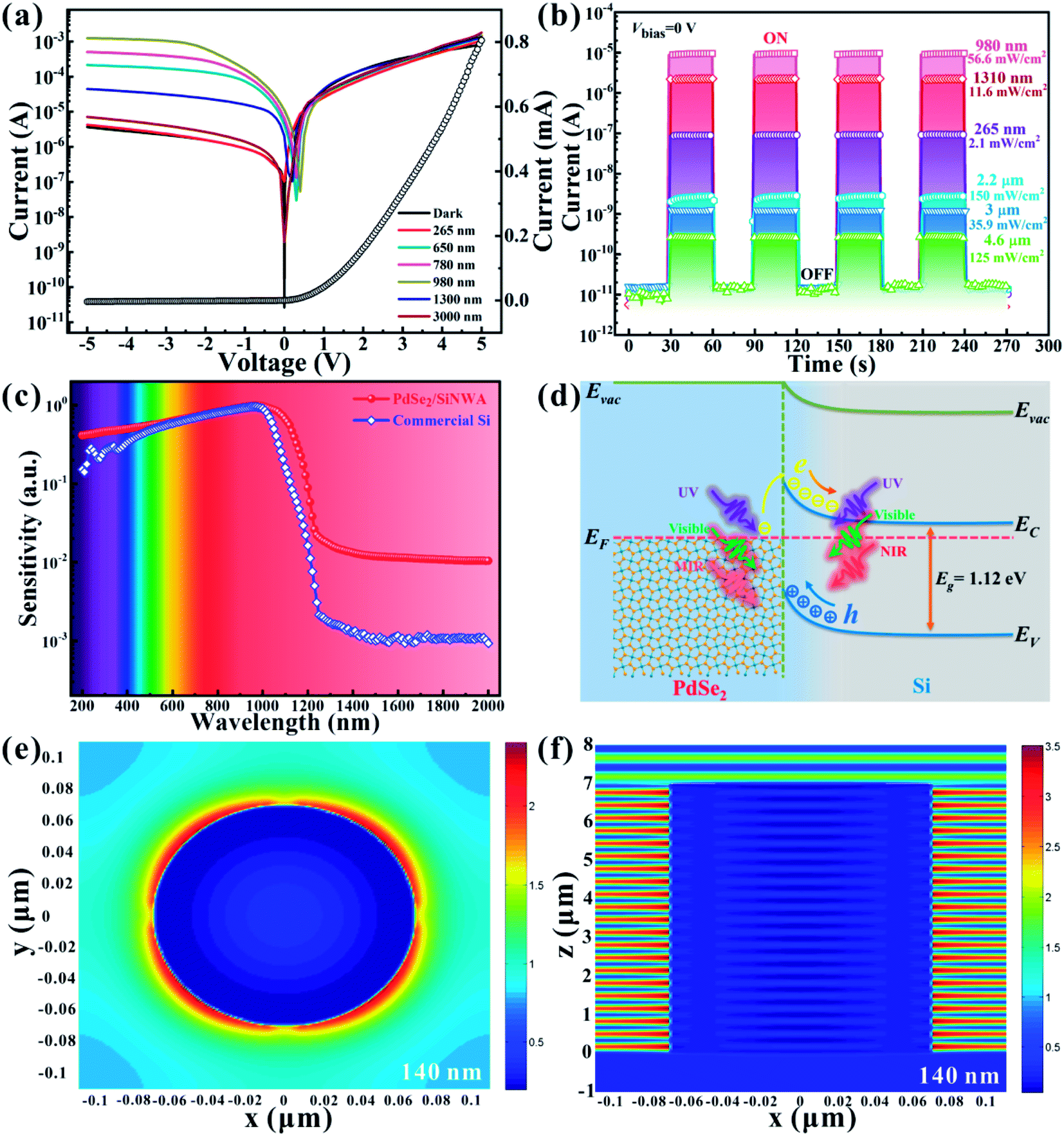 | ||
| Fig. 2 (a) I–V curves and (b) time-resolved photoresponse properties of a PdSe2/SiNWA heterostructure device under light illumination with different wavelengths at a constant intensity. (c) Photoresponse spectra of the PdSe2/SiNWA heterostructure device and the commercial Si photodetector (DSi200, Zolix). (d) Energy band diagram of the PdSe2/SiNWA heterostructure under light illumination. (e and f) Simulated electric field energy distribution for the PdSe2/SiNWA with a diameter of 140 nm. | ||
To shed light on the excellent photoresponse properties of the photovoltaic detector, simulations of electric field energy density distribution of the devices were performed using FDTD simulations. Fig. 2e and f present the electric field energy distribution of the PdSe2/SiNWA heterostructure with a NW diameter of 140 nm under 980 nm unpolarized light. And the electric field energy distributions for the NWs with different sizes are shown in Fig. S5.† It can be observed that the incident light is mainly trapped in gaps between the NWs. In particular, the electric field is greatly enhanced at the side surfaces of NWs. One can thus expect significant absorption enhancement because the overall area of side surfaces of NWs is much larger than that of the single surface of bulk silicon.
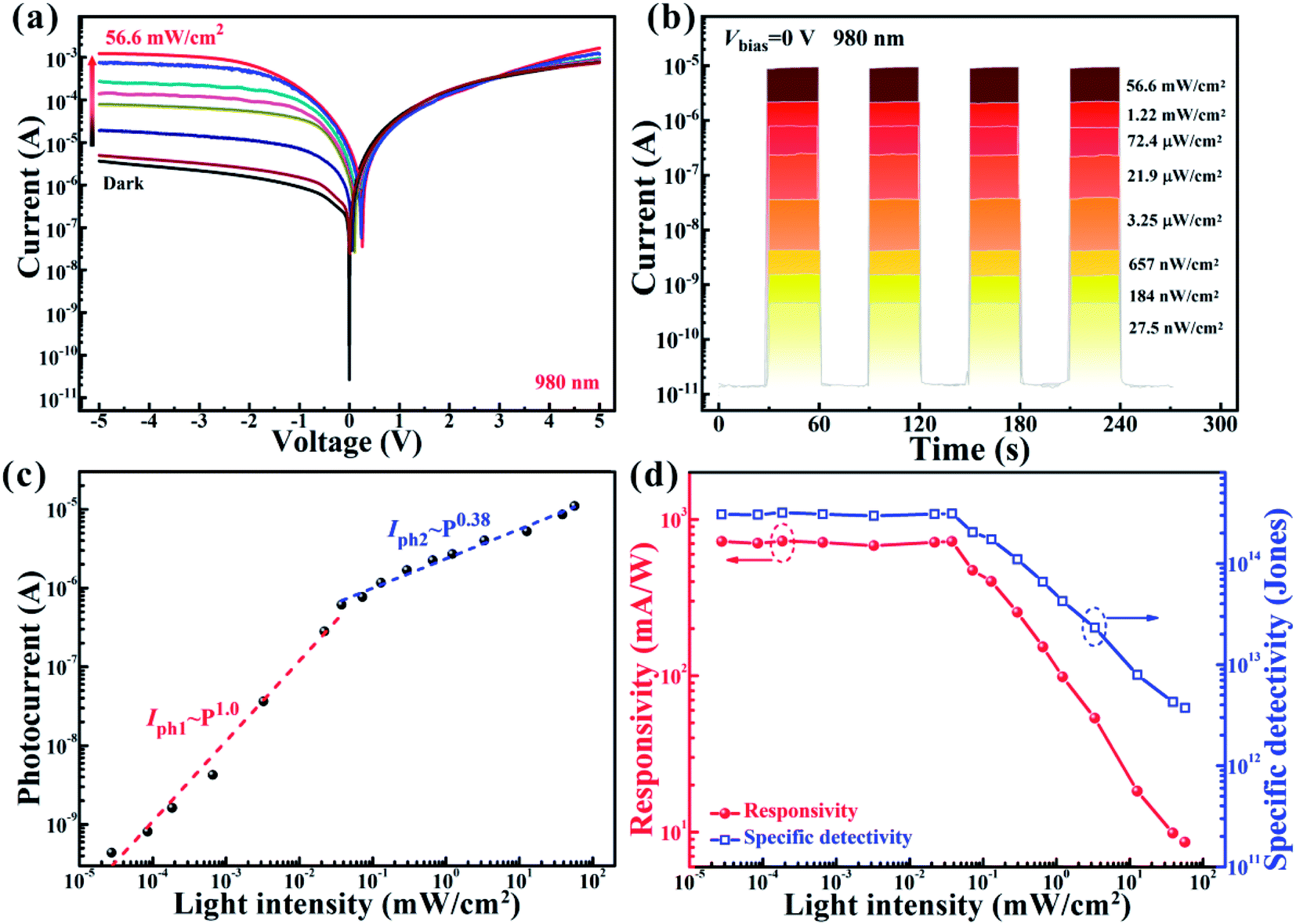
The photoresponse properties of the PdSe2/SiNWA heterostructure device are strongly dependent on the power intensity of incident light. Fig. 3a shows the I–V curves of the photovoltaic detector measured under 980 nm light with different intensities. It is noted that the current at reverse bias increases gradually with the increasing light intensity from 0.07 to 56.6 mW cm−2. A maximum open-circuit voltage (VOC) of 0.26 V and a short-circuit current (ISC) of 7.5 μA are achieved at a power intensity of 56.6 mW cm−2 (Fig. S6†). Even though the power conversion efficiency of the device is not so high (∼0.1%), it is high enough to enable the device to operate at zero bias without an external power supply. Moreover, the low dark current at zero bias leads to an Ion/Ioff as high as 106 at 56.6 mW cm−2 with excellent stability and reproducibility (Fig. 3b), which is much larger than the value of the SiNWA (∼1.1, Fig. S7†). The Ion/Ioff is 34.3 even at an ultralow light intensity of 27.5 nW cm−2. This result demonstrates the high sensitivity of the PdSe2/SiNWA heterostructure photovoltaic detector with the capability of detecting ultraweak light signals. As a matter of fact, the dependence of extracted photocurrent on power intensity can be described by the power law: I = APα, where the exponent α represents the recombination of photoexcited carriers.48 By fitting the data in a relatively low light intensity range (Fig. 3c), an ideal exponent of α ≈ 1.0 was obtained, while a non-ideal value of 0.38 was obtained in a high light intensity region. The value is less than one at a higher light intensity due to the enhanced recombination loss and the existence of trap states at the junction interface.6,49 In addition, the linear dynamic range (LDR) of a photodetector is the maximum linear response relative to its noise, which can be given by the following formula:36
 | (1) |
 is the photocurrent measured at a light intensity of 1 mW cm−2, and ID is the dark current at zero bias (Fig. S8†). A large LDR of 108.3 dB was calculated at zero bias, which is comparable with that of a commercial Si photodetector (∼120 dB)50 and superior to that of some 2D/Si heterojunction devices (42–92 dB),44,45,51 commercial InGaAs photodiodes (66 dB),47 and all-graphene p–n heterojunction devices (93 dB).52 Such an excellent photoresponse performance is reasonably ascribed to the enhanced light absorption characteristics of the PdSe2/SiNWA heterostructure.
 | ||
| Fig. 3 (a) I–V curves and (b) time-resolved photoresponse of the PdSe2/SiNWA photodetector under 980 nm light illumination with varied light intensity. (c) Logarithmic plot of the photocurrent versus light intensity. (d) Responsivity and specific detectivity of the heterostructure photodetector as a function of light intensity. | ||
As the key figures of merit for a photodetector, responsivity (R) and specific detectivity (D*) can be evaluated using the following formulas:53
 | (2) |
 | (3) |
Response speed is another significant parameter for evaluating the ability of a photodetector to follow a rapidly varying optical signal, which can be characterized by calculating the time interval between 10% (or 90%) and 90% (or 10%) of the maximum photocurrent at the rising/falling edge. Fig. 4a depicts the time-resolved photoresponse of the device to 980 nm pulsed light at frequencies of 1, 2 and 5 kHz, respectively, with a normalized photocurrent, showing fast and stable responses to pulsed light signals. From the relative balance [(Imax − Imin)/Imax] shown in Fig. 4b, it is clear that the device can respond to a fast switching light signal of up to 105 Hz, and possesses a high 3 dB frequency (f3dB) of ∼8 kHz. By further analysis of each of the edges of response, the response speeds of the PdSe2/SiNWA heterostructure photovoltaic detector can be obtained to be 25.1/34 μs at 8 kHz (Fig. 3c). The capability of this photovoltaic detector to follow a rapidly varied pulsed signal was further investigated by using a pulsed laser light of 266 nm at 1 kHz with a pulse width of 1 ns. In Fig. 4d and e, each pulse signal can be well identified with an ultrafast rising time of 126 ns, revealing the capability of the device to detect nanosecond pulsed light signals. Significantly, the comprehensive performance of the PdSe2/SiNWA heterostructure photovoltaic detector is superior to that of recently reported 2D layered material-based infrared photodetectors, as summarized in Table 1.
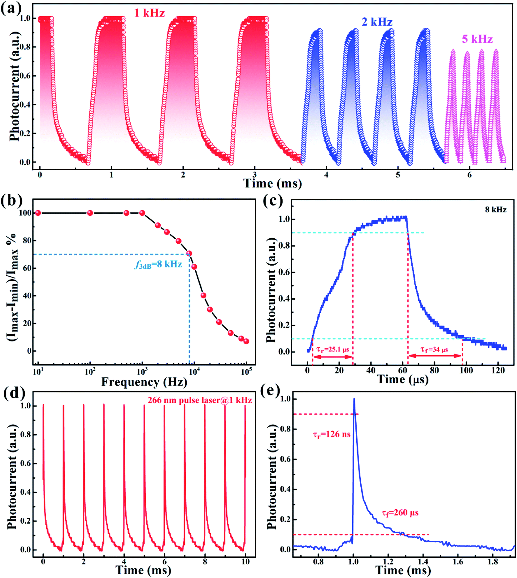 | ||
| Fig. 4 (a) Time-resolved photoresponses of the PdSe2/SiNWA heterostructure to 980 nm pulsed light with frequencies of 1, 2 and 5 kHz, respectively. (b) Relative balance [(Imax − Imin)/Imax] as a function of switching frequency. (c) Response speeds at 8 kHz. (d) The photoresponse of the heterostructure device to 266 nm pulsed laser light at 1 kHz with a pulse width of 1 ns. (e) An enlarged response cycle for evaluating the response speed. | ||
| Devices | λ [μm] | I on/Ioff | R [mA W−1] | D* [Jones] | Response speed [μs] | Ref. |
|---|---|---|---|---|---|---|
| PdSe2/SiNWA | 0.2–4.6 | 106 | 726 | 3.19 × 10¹⁴ | 3.4/3.9 (100 kHz) | This work |
| PdSe2/Si | 0.2–3 | ∼105 | 300 | ∼1013 | 38/44 (5 kHz) | 28 |
| PdSe2/Ge | 0.2–3 | 105 | 691 | 1.73 × 10¹³ | 6.4/92.5 (5 kHz) | 37 |
| PdSe2/GeNCA | 0.2–2.2 | <104 | 530 | 1.45 × 10¹¹ | 25.4/38.5 (20 kHz) | 69 |
| PdSe2/MoS2 | 0.45–10.6 | ∼104 | 185.6 | 1.73 × 10¹³ | 65.3/62.4 (1 kHz) | 30 |
| PtSe2/SiNWA | 0.2–1.55 | ∼104 | 18.4 | 3.26 × 10¹¹ | 10.1/19.5 (10 kHz) | 45 |
| MoS2/SiNWA | 0.2–1.2 | ∼105 | 298 | 2.8 × 10¹³ | 2.9/7.3 (50 kHz) | 44 |
In addition to these impressive photoresponse characteristics, the PdSe2/SiNWA heterostructure-based device also shows very high sensitivity to polarized light signals, which originates from the pentagonally arranged asymmetric crystal structure of PdSe2 with a puckered morphology.31Fig. 5a shows a schematic diagram of the experimental setup based on the present PdSe2/SiNWA device. A polarizer can turn an incident light into a polarized light, and the polarization angle can be adjusted by using a half-wave plate. The polarization angle-dependent photocurrent is plotted in Fig. 5b, which has been normalized according to the minimum value. From the measured photocurrent at zero bias, the photocurrent is found to reach a maximum value at 0° (180°), while a minimum value is obtained at 90° (270°), giving rise to a high polarization sensitivity of 75. It is noteworthy that this value is much larger than that obtained for other 2D layered material-based devices, such as GeS2 (2.1)54 and black phosphorus/MoS2 (22),55 revealing the great potential of the photodetector for obtaining polarimetric information, high-contrast polarizers and optical switch applications.56 The highly polarization-sensitive photodetection performance of the PdSe2/SiNWA heterojunction could be attributed to the following reasons. First, the high asymmetry of the 2D PdSe2 films leads to strong anisotropic properties.31 Second, the low dark current of the heterojunction at zero bias is beneficial to improve the polarization sensitivity.57 Third, the built-in perpendicular electric field in the vertical heterojunction can effectively and quickly separate the photogenerated carriers, and reduce the carrier recombination during charge transport.13
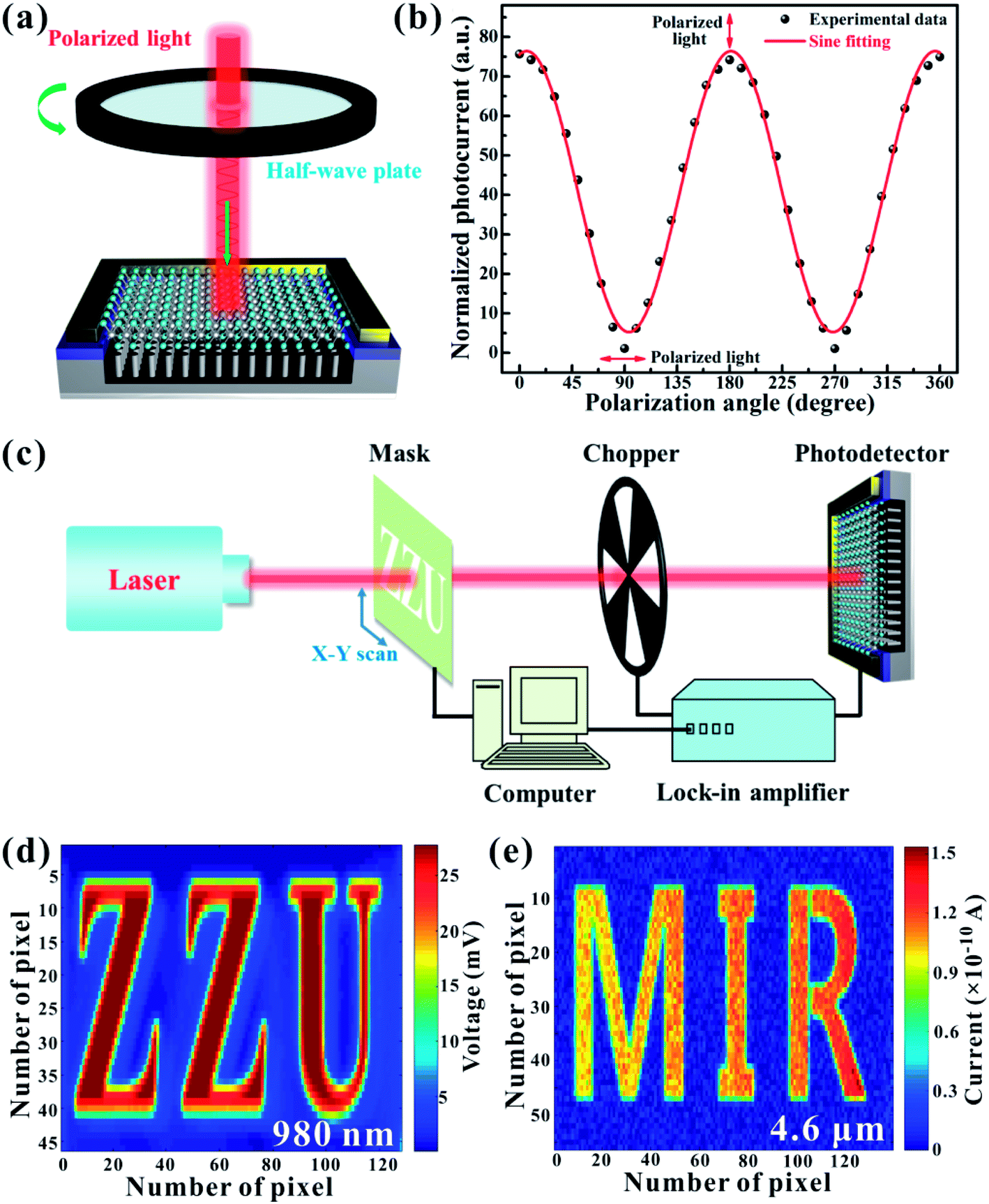 | ||
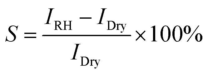
| Fig. 5 (a) Schematic diagram of the experimental setup for polarization sensitivity measurement. (b) Normalized photocurrent of the heterostructure as a function of the polarization angle. (c) Schematic illustration of the measurement setup for imaging application. The imaging results of the (d) “ZZU” pattern under 980 nm illumination and (e) “MIR” pattern under 4.6 μm illumination, respectively. | ||
As one of the most important functionalities of photodetectors, the imaging ability of photodetectors has attracted tremendous interest due to their great importance in both civilian and military fields.58,59 In view of the outstanding photoresponse capability of the PdSe2/SiNWA heterostructure photovoltaic detector, the infrared image sensing ability of the current device was further explored. Fig. 5c displays a schematic diagram of the measurement setup for an imaging sensor, in which lasers of 980 nm and 4.6 μm were used to provide infrared signals, and metal masks with hollow “ZZU” and “MIR” patterns fixed on a 2D motorized stage were placed between the light sources and detector. During the image-sensing process, the electrical signals (voltage or current) of the PdSe2/SiNWA heterostructure photovoltaic detector were collected by using a lock-in amplifier, and then the apparent 2D contrast mapping images of the “ZZU” pattern for 980 nm and the “MIR” pattern for 4.6 μm (Fig. 5d and e) were generated. It should be pointed out that high-resolution imaging results with a voltage contrast ratio of over 103 for 980 nm and a current contrast ratio of over 102 for 4.6 μm were obtained, verifying the excellent infrared imaging capability of the as-assembled PdSe2/SiNWA photovoltaic detector.
Due to the large surface-to-volume ratio of both the 2D PdSe2 film and the SiNWA, the PdSe2/SiNWA heterostructure device shows high sensitivity to the relative humidity (RH) of the surrounding atmosphere. In this work, we further explored the humidity sensing properties of the device. Fig. 6a and b show the response properties of the PdSe2/SiNWA heterostructure to different RH values from 11% to 95% in the dark and under 780 nm illumination, respectively, at room temperature. It is observed that significant current response with good stability and repeatability is achieved at each of the RH values. The sensitivity (S) of a humidity sensor can be defined by the following equation:60
 | (4) |
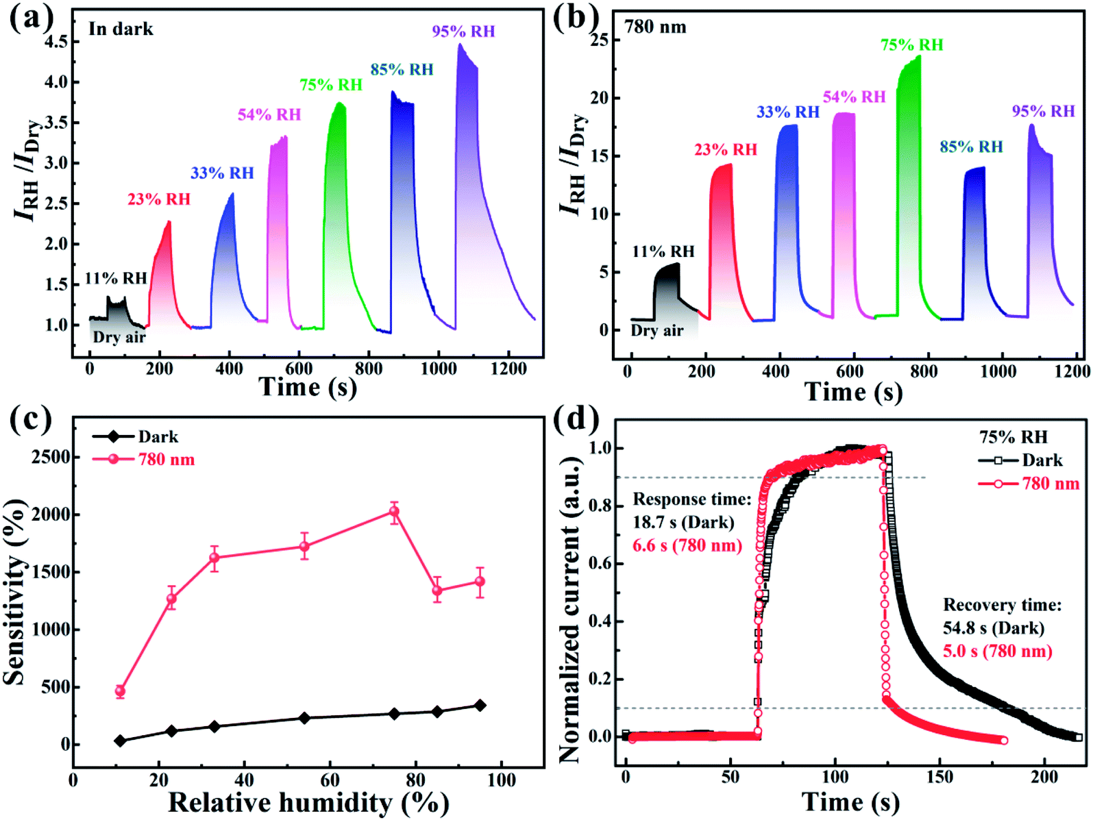 | ||
| Fig. 6 The response properties of the PdSe2/SiNWA heterostructure to different RH values (a) in the dark and (b) under 780 nm illumination. (c) The dependence relationship between sensitivity and relative humidity in the dark and under 780 nm illumination. (d) The response and recovery time of the device to 75% RH in the dark and under 780 nm illumination. | ||
Conclusions
In summary, we have demonstrated a self-driven, broadband and polarization-sensitive photovoltaic detector made of the PdSe2/SiNWA mixed-dimensional vdW heterostructure. The device is highly sensitive to an ultra-broadband spectrum ranging from DUV to MIR (200 nm to 4.6 μm) with a high responsivity of 726 mA W−1, a large specific detectivity of 3.19 × 10¹⁴ Jones, a fast response speed of 25.1/34 μs, and an ultrahigh polarization sensitivity of 75. Based on the FDTD calculation, the remarkable device performance could be ascribed to the strong light confinement effect induced by Si nanostructures. Also, the as-assembled device can readily record simple images of “ZZU” and “MIR” produced under 980 and 4600 nm illumination, respectively, due to the excellent imaging capability. Moreover, this PdSe2/SiNWA heterostructure device showed light-enhanced humidity sensing properties with a high sensitivity and a fast response/recovery time. These remarkable results suggest that the PdSe2/SiNWA mixed-dimensional heterostructure device will have great potential application in high-performance polarization-sensitive broadband photodetection, infrared imaging and humidity sensing.Conflicts of interest
There are no conflicts to declare.Acknowledgements
This work was financially supported by the National Natural Science Foundation of China (Nos. 51821002, 91833303, 11974016 and 61605174), the Priority Academic Program Development of Jiangsu Higher Education Institutions (PAPD), the 111 Project, the Collaborative Innovation Center of Suzhou Nano Science and Technology (Nano-CIC), and the Natural Science Foundation of Anhui Province (808235830016).Notes and references
- A. K. Geim and K. S. Novoselov, Nat. Mater., 2007, 6, 183–191 CrossRef CAS PubMed.
- X. Wang, Z. Cheng, K. Xu, H. K. Tsang and J.-B. Xu, Nat. Photonics, 2013, 7, 888–891 CrossRef CAS.
- S. Du, W. Lu, A. Ali, P. Zhao, K. Shehzad, H. Guo, L. Ma, X. Liu, X. Pi, P. Wang, H. Fang, Z. Xu, C. Gao, Y. Dan, P. Tan, H. Wang, C. T. Lin, J. Yang, S. Dong, Z. Cheng, E. Li, W. Yin, J. Luo, B. Yu, T. Hasan, Y. Xu, W. Hu and X. Duan, Adv. Mater., 2017, 29, 1700463 CrossRef PubMed.
- J. Zhu, D. Yang, Z. Yin, Q. Yan and H. Zhang, Small, 2014, 10, 3480–3498 CrossRef CAS PubMed.
- F. Koppens, T. Mueller, P. Avouris, A. Ferrari, M. Vitiello and M. Polini, Nat. Nanotechnol., 2014, 9, 780–793 CrossRef CAS PubMed.
- L.-H. Zeng, M.-Z. Wang, H. Hu, B. Nie, Y.-Q. Yu, C.-Y. Wu, L. Wang, J.-G. Hu, C. Xie, F.-X. Liang and L.-B. Luo, ACS Appl. Mater. Interfaces, 2013, 5, 9362–9366 CrossRef CAS PubMed.
- H. Li, Y. Li, A. Aljarb, Y. Shi and L. J. Li, Chem. Rev., 2018, 118, 6134–6150 CrossRef CAS PubMed.
- X. Zhang, H. Cheng and H. Zhang, Adv. Mater., 2017, 29, 1701704 CrossRef PubMed.
- C. Kamal and M. Ezawa, Phys. Rev. B, 2015, 91, 085423 CrossRef.
- Y. Yi, Z. Sun, J. Li, P. K. Chu and X. F. Yu, Small Methods, 2019, 3, 1900165 CrossRef CAS.
- J. Ji, X. Song, J. Liu, Z. Yan, C. Huo, S. Zhang, M. Su, L. Liao, W. Wang, Z. Ni, Y. Hao and H. Zeng, Nat. Commun., 2016, 7, 13352 CrossRef CAS PubMed.
- L. Tao, E. Cinquanta, D. Chiappe, C. Grazianetti, M. Fanciulli, M. Dubey, A. Molle and D. Akinwande, Nat. Nanotechnol., 2015, 10, 227 CrossRef CAS PubMed.
- P. Xiao, J. Mao, K. Ding, W. Luo, W. Hu, X. Zhang, X. Zhang and J. Jie, Adv. Mater., 2018, 30, 1801729 CrossRef PubMed.
- J. Mao, Y. Yu, L. Wang, X. Zhang, Y. Wang, Z. Shao and J. Jie, Adv. Sci., 2016, 3, 1600018 CrossRef PubMed.
- E. Wu, D. Wu, C. Jia, Y. Wang, H. Yuan, L. Zeng, T. Xu, Z. Shi, Y. Tian and X. Li, ACS Photonics, 2019, 6, 565–572 CrossRef CAS.
- R. Zhuo, Y. Wang, D. Wu, Z. Lou, Z. Shi, T. Xu, J. Xu, Y. Tian and X. Li, J. Mater. Chem. C, 2018, 6, 299–303 RSC.
- D. J. Late, R. V. Kanawade, P. K. Kannan and C. S. Rout, Sens. Lett., 2016, 14, 1249–1254 CrossRef.
- D. J. Late, T. Doneux and M. Bougouma, Appl. Phys. Lett., 2014, 105, 233103 CrossRef.
- D. J. Late, Y.-K. Huang, B. Liu, J. Acharya, S. N. Shirodkar, J. Luo, A. Yan, D. Charles, U. V. Waghmare, V. P. Dravid and C. N. R. Rao, ACS Nano, 2013, 7, 4879–4891 CrossRef CAS PubMed.
- Y. Huang, E. Sutter, N. N. Shi, J. Zheng, T. Yang, D. Englund, H. J. Gao and P. Sutter, ACS Nano, 2015, 9, 10612–10620 CrossRef CAS PubMed.
- D. Parviz, F. Irin, S. A. Shah, S. Das, C. B. Sweeney and M. J. Green, Adv. Mater., 2016, 28, 8796–8818 CrossRef CAS PubMed.
- P. Ranjan, T. K. Sahu, R. Bhushan, S. S. Yamijala, D. J. Late, P. Kumar and A. Vinu, Adv. Mater., 2019, 31, e1900353 CrossRef PubMed.
- Q. He, P. Li, Z. Wu, B. Yuan, Z. Luo, W. Yang, J. Liu, G. Cao, W. Zhang, Y. Shen, P. Zhang, S. Liu, G. Shao and Z. Yao, Adv. Mater., 2019, 31, e1901578 CrossRef PubMed.
- P. Yang, X. Zou, Z. Zhang, M. Hong, J. Shi, S. Chen, J. Shu, L. Zhao, S. Jiang, X. Zhou, Y. Huan, C. Xie, P. Gao, Q. Chen, Q. Zhang, Z. Liu and Y. Zhang, Nat. Commun., 2018, 9, 979 CrossRef PubMed.
- C. Tan, X. Cao, X. J. Wu, Q. He, J. Yang, X. Zhang, J. Chen, W. Zhao, S. Han, G. H. Nam, M. Sindoro and H. Zhang, Chem. Rev., 2017, 117, 6225–6331 CrossRef CAS PubMed.
- Y. Liu, N. O. Weiss, X. Duan, H.-C. Cheng, Y. Huang and X. Duan, Nat. Rev. Mater., 2016, 1, 16042 CrossRef CAS.
- D. Wu, Y. Wang, L. Zeng, C. Jia, E. Wu, T. Xu, Z. Shi, Y. Tian, X. Li and Y. H. Tsang, ACS Photonics, 2018, 5, 3820–3827 CrossRef CAS.
- L.-H. Zeng, D. Wu, S.-H. Lin, C. Xie, H.-Y. Yuan, W. Lu, S. P. Lau, Y. Chai, L.-B. Luo, Z.-J. Li and Y. H. Tsang, Adv. Funct. Mater., 2019, 29, 1806878 CrossRef.
- L.-H. Zeng, Q.-M. Chen, Z.-X. Zhang, D. Wu, H. Yuan, Y.-Y. Li, W. Qarony, S. P. Lau, L.-B. Luo and Y. H. Tsang, Adv. Sci., 2019, 6, 1901134 CrossRef CAS PubMed.
- M. Long, Y. Wang, P. Wang, X. Zhou, H. Xia, C. Luo, S. Huang, G. Zhang, H. Yan, Z. Fan, X. Wu, X. Chen, W. Lu and W. Hu, ACS Nano, 2019, 13, 2511–2519 CAS.
- A. D. Oyedele, S. Yang, L. Liang, A. A. Puretzky, K. Wang, J. Zhang, P. Yu, P. R. Pudasaini, A. W. Ghosh, Z. Liu, C. M. Rouleau, B. G. Sumpter, M. F. Chisholm, W. Zhou, P. D. Rack, D. B. Geohegan and K. Xiao, J. Am. Chem. Soc., 2017, 139, 14090–14097 CrossRef CAS PubMed.
- E. Li, D. Wang, P. Fan, R. Zhang, Y.-Y. Zhang, G. Li, J. Mao, Y. Wang, X. Lin, S. Du and H.-J. Gao, Nano Res., 2018, 11, 5858–5865 CrossRef CAS.
- W. L. Chow, P. Yu, F. Liu, J. Hong, X. Wang, Q. Zeng, C. H. Hsu, C. Zhu, J. Zhou, X. Wang, J. Xia, J. Yan, Y. Chen, D. Wu, T. Yu, Z. Shen, H. Lin, C. Jin, B. K. Tay and Z. Liu, Adv. Mater., 2017, 29, 1602969 CrossRef PubMed.
- Q. Liang, Q. Wang, Q. Zhang, J. Wei, S. X. Lim, R. Zhu, J. Hu, W. Wei, C. Lee, C. Sow, W. Zhang and A. T. S. Wee, Adv. Mater., 2019, 31, e1807609 CrossRef PubMed.
- D. Jariwala, T. J. Marks and M. C. Hersam, Nat. Mater., 2017, 16, 170–181 CrossRef CAS PubMed.
- R. Zhuo, L. Zeng, H. Yuan, D. Wu, Y. Wang, Z. Shi, T. Xu, Y. Tian, X. Li and Y. H. Tsang, Nano Res., 2019, 12, 183–189 CrossRef CAS.
- D. Wu, J. Guo, J. Du, C. Xia, L. Zeng, Y. Tian, Z. Shi, Y. Tian, X. J. Li, Y. H. Tsang and J. Jie, ACS Nano, 2019, 13, 9907–9917 CrossRef CAS PubMed.
- Y. Wang, X. Huang, D. Wu, R. Zhuo, E. Wu, C. Jia, Z. Shi, T. Xu, Y. Tian and X. Li, J. Mater. Chem. C, 2018, 6, 4861–4865 RSC.
- J. Wang, J. Han, X. Chen and X. Wang, InfoMat, 2019, 1, 33–53 CrossRef.
- H. Qiao, Z. Huang, X. Ren, S. Liu, Y. Zhang, X. Qi and H. Zhang, Adv. Opt. Mater., 2020, 8, 1900765 CrossRef CAS.
- R. A. Soref, Proc. IEEE, 1993, 81, 1687–1706 CrossRef CAS.
- Y. Cui, Z. H. Zhong, D. L. Wang, W. U. Wang and C. M. Lieber, Nano Lett., 2003, 3, 149–152 CrossRef CAS.
- M. H. R. Lankhorst, B. W. S. M. M. Ketelaars and R. A. M. Wolters, Nat. Mater., 2005, 4, 347–352 CrossRef CAS PubMed.
- D. Wu, Z. Lou, Y. Wang, Z. Yao, T. Xu, Z. Shi, J. Xu, Y. Tian, X. Li and Y. H. Tsang, Sol. Energy Mater. Sol. Cells, 2018, 182, 272–280 CrossRef CAS.
- L. Zeng, S. Lin, Z. Lou, H. Yuan, H. Long, Y. Li, W. Lu, S. P. Lau, D. Wu and Y. H. Tsang, NPG Asia Mater., 2018, 10, 352–362 CrossRef CAS.
- E. D. Palik, Handbook of Optical Constants of Solids, Academic Press, Orlando, 1985 Search PubMed.
- P. Wang, S. Liu, W. Luo, H. Fang, F. Gong, N. Guo, Z. G. Chen, J. Zou, Y. Huang, X. Zhou, J. Wang, X. Chen, W. Lu, F. Xiu and W. Hu, Adv. Mater., 2017, 29, 1604439 CrossRef PubMed.
- L. Wang, J. Jie, Z. Shao, Q. Zhang, X. Zhang, Y. Wang, Z. Sun and S. T. Lee, Adv. Funct. Mater., 2015, 25, 2910–2919 CrossRef CAS.
- S.-C. Kung, W. E. van der Veer, F. Yang, K. C. Donavan and R. M. Penner, Nano Lett., 2010, 10, 1481–1485 CrossRef CAS PubMed.
- L. Dou, Y. M. Yang, J. You, Z. Hong, W. H. Chang, G. Li and Y. Yang, Nat. Commun., 2014, 5, 5404 CrossRef CAS PubMed.
- R. K. Chowdhury, R. Maiti, A. Ghorai, A. Midya and S. K. Ray, Nanoscale, 2016, 8, 13429–13436 RSC.
- C. O. Kim, S. Kim, D. H. Shin, S. S. Kang, J. M. Kim, C. W. Jang, S. S. Joo, J. S. Lee, J. H. Kim, S. H. Choi and E. Hwang, Nat. Commun., 2014, 5, 3249 CrossRef PubMed.
- L.-H. Zeng, S.-H. Lin, Z.-J. Li, Z.-X. Zhang, T.-F. Zhang, C. Xie, C.-H. Mak, Y. Chai, S. P. Lau, L.-B. Luo and Y. H. Tsang, Adv. Funct. Mater., 2018, 28, 1705970 CrossRef.
- Y. Yang, S.-C. Liu, X. Wang, Z. Li, Y. Zhang, G. Zhang, D.-J. Xue and J.-S. Hu, Adv. Funct. Mater., 2019, 29, 1900411 CrossRef.
- J. Bullock, M. Amani, J. Cho, Y.-Z. Chen, G. H. Ahn, V. Adinolfi, V. R. Shrestha, Y. Gao, K. B. Crozier, Y.-L. Chueh and A. Javey, Nat. Photonics, 2018, 12, 601–607 CrossRef CAS.
- L. Li, W. Han, L. Pi, P. Niu, J. Han, C. Wang, B. Su, H. Li, J. Xiong, Y. Bando and T. Zhai, InfoMat, 2019, 1, 54–73 CrossRef.
- H. Yuan, X. Liu, F. Afshinmanesh, W. Li, G. Xu, J. Sun, B. Lian, A. G. Curto, G. Ye, Y. Hikita, Z. Shen, S. C. Zhang, X. Chen, M. Brongersma, H. Y. Hwang and Y. Cui, Nat. Nanotechnol., 2015, 10, 707–713 CrossRef CAS PubMed.
- W. Deng, X. Zhang, L. Huang, X. Xu, L. Wang, J. Wang, Q. Shang, S. T. Lee and J. Jie, Adv. Mater., 2016, 28, 2201–2208 CrossRef CAS PubMed.
- L. Li, Z. Lou and G. Shen, Adv. Funct. Mater., 2018, 28, 1705389 CrossRef.
- A. S. Pawbake, R. G. Waykar, D. J. Late and S. R. Jadkar, ACS Appl. Mater. Interfaces, 2016, 8, 3359–3365 CrossRef CAS PubMed.
- Z. Lou, D. Wu, K. Bu, T. Xu, Z. Shi, J. Xu, Y. Tian and X. Li, J. Alloys Compd., 2017, 726, 632–637 CrossRef CAS.
- M. B. Erande, M. S. Pawar and D. J. Late, ACS Appl. Mater. Interfaces, 2016, 8, 11548–11556 CrossRef CAS PubMed.
- L. D. Bharatula, M. B. Erande, I. S. Mulla, C. S. Rout and D. J. Late, RSC Adv., 2016, 6, 105421–105427 RSC.
- A. S. Pawbake, S. R. Jadkar and D. J. Late, Mater. Res. Express, 2016, 3, 105038 CrossRef.
- W. Li, E. Dai, G. Bai and J. Xu, Sens. Actuators, B, 2016, 237, 526–533 CrossRef CAS.
- Z. Chen and C. Lu, Sens. Lett., 2005, 3, 274–295 CrossRef CAS.
- Y. M. Juan, S. J. Chang, H. T. Hsueh, S. H. Wang, W. Y. Weng, T. C. Cheng and C. L. Wu, RSC Adv., 2015, 5, 84776–84781 RSC.
- Y. Li, F. Della Valle, M. Simonnet, I. Yamada and J.-J. Delaunay, Appl. Phys. Lett., 2009, 94, 023110 CrossRef.
- L. B. Luo, D. Wang, C. Xie, J. G. Hu, X. Y. Zhao and F. X. Liang, Adv. Funct. Mater., 2019, 29, 1900849 CrossRef.
Footnote |
| † Electronic supplementary information (ESI) available: Fig. S1–S8. See DOI: 10.1039/c9ta13611h |
| This journal is © The Royal Society of Chemistry 2020 |