
Thickness of elemental and binary single atomic monolayers
Peter
Hess

Institute of Physical Chemistry, University of Heidelberg, Im Neuenheimer Feld 253, D-69120 Heidelberg, Germany. E-mail: peter.hess@urz.uni-heidelberg.de
First published on 3rd December 2019
Abstract
The thickness of monolayers is a fundamental property of two-dimensional (2D) materials that has not found the necessary attention. It plays a crucial role in their mechanical behavior, the determination of related physical properties such as heat transfer, and especially the properties of multilayer systems. Measurements of the thickness of free-standing monolayers are widely lacking and notoriously too large. Consistent thicknesses have been reported for single layers of graphene, boronitrene, and SiC derived from interlayer spacing measured by X-ray diffraction in multilayer systems, first-principles calculations of the interlayer spacing, and tabulated van der Waals (vdW) diameters. Furthermore, the electron density-based volume model agrees with the geometric slab model for graphene and boronitrene. For other single-atom monolayers DFT calculations and molecular dynamics (MD) simulations deliver interlayer distances that are often much smaller than the vdW diameter, owing to further electrostatic and (weak) covalent interlayer interaction. Monolayers strongly bonded to a surface also show this effect. If only weak vdW forces exist, the vdW diameter delivers a reasonable thickness not only for free-standing monolayers but also for few-layer systems and adsorbed monolayers. Adding the usually known corrugation effect of buckled or puckered monolayers to the vdW diameter delivers an upper limit of the monolayer thickness. The study presents a reference database of thickness values for elemental and binary group-IV and group-V monolayers, as well as binary III–V and IV–VI compounds.
1. Introduction
With the realization of single atomic layers the ultimate scaling in thickness has been reached. However, to date the actual thickness of most monolayers has been neither measured nor calculated with the necessary accuracy. The enormous difficulties encountered in an accurate direct measurement of the thickness of free-standing monolayers, e.g., by nanoindentation using atomic force microscopy (AFM), can be seen in the range of values reported for the best studied compound graphene, varying between 0.4 and 1.7 nm.1 Only by applying sophisticated sample preparation and accurate imaging techniques a reproducible thickness of 0.43 nm could be realized, which approaches the currently accepted value of 3.35 nm, derived for graphite.2 One reason for the systematic overestimation of thickness originates from overlayers of the solvent in solution-processed monolayer preparation.3The layer thickness controls not only relevant properties of monolayers such as their mechanical behavior and heat conductivity4 but to an even larger extend the optical and electronic properties of few-layer and multilayer systems such as the band gap. The latter find increasing attention for tuning physical properties with the number of layers.5 Since for most two-dimensional (2D) materials accurate experimental thickness values of free-standing monolayers are still lacking, first-principles theory plays a dominant role in estimating thicknesses, mainly by calculating the thickness of bi-, tri-, and few-layer systems. If the corresponding layered crystal exists, the interlayer spacing can been determined experimentally, for example, by X-ray diffraction (XRD)6 and high-resolution transmission electron microscopy (HRTEM).7
A presentation of the mechanical properties of 2D materials is possible by either 2D or 3D quantities. The 3D description uses bulk units such as N m−2 for the Young's modulus and ultimate strength and implies the knowledge of the layer thickness or layer volume, which usually is not rigorously known. The 3D properties allow a comparison with those of well-known bulk materials, for example, graphene versus diamond. However, one has always to keep in mind that monolayers are not real 3D entities, owing to the restriction of one dimension to an atomic-scale length. Moreover, it is not possible to measure 3D quantities.
By using the mechanical 2D model we take 2D units, for example, N m−1 for the Young's modulus and critical strength. Of course, 2D solids are also not 2D objects in the strict mathematical sense. Formally, however, the simple model of a continuum plane can be employed for a useful description of layers with atomic thickness. Properties with 2D units are accessible by experiment and a direct comparison with other monolayers is possible since there is no dependence on an assumed monolayer thickness. For this reason, 2D properties are preferable in a comparative study of monolayers. The boundaries of a monolayer do not allow a straightforward derivation of the mechanically active volume or layer thickness. The introduction of simple geometrical volume models, such as a uniform slab with defined thickness, solve the problem to perform the dimensional transformation from measured 2D to quasi 3D units.
As mentioned above, the knowledge of the layer thickness is not only an essential prerequisite to understand the behavior of monolayers but it is also crucial for the determination of physical properties of layered materials. van der Waals (vdW) forces have a minor influence on the bond length and bonding energy of 2D covalent networks, however, they control the cohesion of the whole layered assembly and thus key properties of few-layer systems. Not only vdW forces, but also electrostatic interaction and covalent bonding of the stacked structure, determine the interlayer spacing. Note that the bottom-up synthesis of layered compounds, using monolayers as building blocks and weak vdW interaction, opens a huge new field of artificially assembled 2D materials. Combining monolayers with specific properties may lead to vdW superlattices and heterostructures of technological importance.8
An often-used procedure to determine the thickness is the application of the geometric volume model of a rectangular slab with a thickness taken from the interlayer spacing of the corresponding layered crystal. If such a layered three-dimensional (3D) crystal exists, it is possible to measure the spacing by X-ray experiments or HRTEM. The vdW diameter delivers comparable thicknesses if the interlayer interaction is based on weak vdW forces. However, depending on hybridization interlayer chemical bonding may occur and a strong reduction of the interlayer separation makes the interlayer spacing no longer suitable to estimate the thickness of the free-standing monolayer. Unfortunately, the information on the interlayer interaction energy needed for such a judgement of the layer spacing is quite limited. Of course, these experimental approaches are not applicable in the case of entirely synthetic monolayers without layered structure.
Ab initio calculations are the first choice to compute the pristine structure as well as chemical and physical properties of 2D materials. Besides the prediction of new stable 2D materials, routes of synthesis could be proposed. From the two main theoretical approaches, namely the wave-function-based methods and density functional theory (DFT) calculations, the latter one is more often employed. Here the many-body system of electrons is treated by considering non-interacting electrons moving in an effective potential. To take the exchange and correlation effects into account in the calculation of electron density, the generalized gradient approximation (GGA) is employed that most often uses the Perdew–Burke–Ernzerhof (PBE) functions. Alternatively, but seldom for 2D materials the local density approximation (LDA), in the form of Ceperley–Alder (CA) and parameterized by Perdew–Zunger (PZ), is employed. In the treatment of few-layer systems larger differences between the GGA and LDA approach may be observed.
Owing to the lack of measurements, theoretical methods such as DFT and molecular dynamics (MD) currently play an essential role in elucidating the layered structure of few-layer systems. This includes the stability of different stacking configurations of bi-, tri-, and multi-layer systems. Since in layered materials strong intralayer covalent bonding and weak interlayer dispersion forces are simultaneously in action present theoretical approaches have serious problems to accurately describe these soft materials. Therefore, it is not surprising that even for the best studied compounds graphite and boron nitride the suggested interlayer binding energies vary between 24 and 86 meV per atom.9,10 These values have been calculated for the most stable stacking configuration of bilayers and bulk crystals, which to some extent have different interlayer interaction. In most cases, however, the main uncertainties originate from the theoretical approximations employed.
An alternative concept for an estimate of the monolayer thickness is the use of tabulated vdW radii, which describe the size of an atom. More accurately, the vdW diameter defines the distance of closest approach of atoms (‘hard-sphere model’). Note that different sets of such compilations of atom sizes, with slightly different vdW radii, are available in the literature for the elements of the periodic table. The vdW diameters are employed here to estimate the thickness of planar elemental and binary monolayers.
The use of vdW radii may have a limited scope of applicability to nano-objects because simple geometrical models may not describe the reality of arbitrary nanoscale objects. In fact, the size and shape of atoms and their bonding configurations are determined by the electron density.11 Therefore, a more accurate but also more elaborate geometry-independent approach based on DFT calculations of electron density has been applied to graphene and boronitrene, resulting in thickness values in very good agreement with those obtained by the simple geometrical slab model.12
This finding reveals that the slab model is a valuable approximation for planar monolayers. Unfortunately, up to now no DFT calculations on the electron density-based volume are available for buckled and puckered monolayers. It would be of great interest to compare electron density-based volumes with those obtained by merely adding the corrugation effect to the vdW diameter, to find a formal thickness of corrugated monolayers. One goal of this study is to compare systematically monolayer thicknesses derived for planar and corrugated monolayers with those of other existing methods, to explore the suitability and limits of the geometrical slab model as simple tool of thickness evaluation.
In the following, we compare the thickness values extracted experimentally and theoretically from the interlayer spacing of layered systems with vdW diameters of elemental and binary group-IV and group-V single atomic monolayers with planar, buckled, or puckered structure. Furthermore, the thickness analysis includes isoelectronic binary group III–V and group IV–VI monolayers. The goal is to compare the information provided by various sources on the thickness of monolayers and to clarify the reasons for the observed deviations. The recommended definition of thickness allows a consistent transformation of measured and calculated properties given in 2D units into those in 3D units. Furthermore, correlations are considered, which exist within groups of structurally and chemically related compounds.13
2. Results
2.1 Thickness of elemental group-IV monolayers
The interlayer spacing of graphite of 0.341 nm, determined by XRD experiments about hundred years ago,6 agrees quite well with the currently accepted theoretical value for the layered graphite structure with AB stacking of 0.335 nm.2 Similarly, detailed calculations of the interlayer spacing, considering dispersive, electrostatic, and Pauli interactions, confirmed a spacing of 0.335 nm.10 Furthermore, these interlayer separations are in very good agreement with the thickness of a single graphene layer of 0.34 nm, as obtained from the standard vdW radii of elements.14 Since the interaction incorporates only vdW forces, the spacing extracted from the multilayer graphite system agrees well with the thickness defined by the vdW diameter. Note that in the case of carbon atoms graphite has been chosen for the definition of the vdW radius and therefore such a good agreement cannot be expected for all elements. The interlayer interaction energies obtained by an improved description of soft layered materials, using vdW-DFT calculations, varied between −22 and −85 meV per atom, depending on the number of layers considered and the approximation employed.9The van der Waals radii used here that were partially introduced by Bondi and represent distances of closest approach. Therefore, they are smaller than gas-phase equilibrium distances.14 More precisely they may be defined as the distance, where the potential energy passes through zero in a head-on collision with negligible kinetic energy.14 Note that a potential change of the free atom size occurring during the formation of the covalent monolayer may be is already included in the definition of the vdW radius. Since a precise determination of the vdW radius is not possible, the tables published by different authors may not agree completely in all elements of the periodic table.
In the electron density-based volume model already mentioned above, the monolayer volume enclosing 99.64% of the total electrons has an average electron density that agrees with the electron density of graphite. This volume has been employed to find the equivalent slab thickness.12 Regardless of surface undulations of the electron distribution in the real monolayer the model delivered a thickness of 0.331 nm, in surprisingly good agreement with the well-established values. The space group of the plane honeycomb monolayer of graphene is P6/mmm.15
Table 1 presents the relevant structural data of the group-IV monolayers, including geometry or space group, vdW diameter, corrugation, thickness values, and theoretical methods. Fig. 1 displays the different results obtained for the monolayer thickness and interlayer spacing. Besides graphene, the other elemental group-IV monolayers (2D-Xenes) silicene, germanene, stanene, and plumbene are attracting increasing attention. They are of great promise for future applications, e.g., as potential 2D topological insulators (TIs), with the quantum spin-Hall (QSH) effect, owing to strong spin–orbit coupling (SOC). In comparison to graphene, in these 2D-Xenes sp2 and sp3 hybridization states compete. In monolayers this leads to low buckling in silicene with a weak π cloud because of a larger sp2 contribution. From silicene to plumbene buckling increases with an increasing contribution of sp3 hybrids in the mixed hybridization states. This is the reason for decreasing π bonding by pz orbitals.16,17
| Geometry space group | vdW diam. dw (nm) | Buckling Δz (nm) | Thickness dw + Δz (nm) | Method monolayer | Inter. spacing dsp (nm) | Inter. bonding (meV per atom) | |
|---|---|---|---|---|---|---|---|
| Graphene | P6/mmm15 | 0.34014 | 016 | 0.340 | DFT-PBE16 | 0.335,10 0.3416 | −(22–85)9,10 |
| Silicene |
P![[3 with combining macron]](https://www.rsc.org/images/entities/char_0033_0304.gif) m120 m120 |
0.42014 | 0.04116 | 0.461 | DFT-PBE16 | 0.321,19 0.3418 | — |
| Germanene | hex., buckl.16 | 0.42214 | 0.06816 | 0.490 | DFT-PBE16 | 0.33519 | −30021 |
| Stanene | hex., buckl.16 | 0.43414 | 0.09016 | 0.524 | DFT-PBE16 | 0.326,24 0.3324 | — |
| Plumbene | hex., buckl.27 | 0.40414 | 0.09327 | 0.497 | First-princip.27 | — | — |
| SiC |
P![[6 with combining macron]](https://www.rsc.org/images/entities/char_0036_0304.gif) m215 m215 |
0.38014 | 028 | 0.380 | DFT-LDA28 | 0.347,30 0.34019 | −(34–55)34 |
| GeC | hex., plane28 | 0.38114 | 028 | 0.381 | DFT-LDA28 | 0.369,32 0.35019 | — |
| SnC | hex., plane28 | 0.38714 | 028 | 0.387 | DFT-LDA28 | — | — |
| GeSi | hex., buckl.19 | 0.42114 | 0.05719 | 0.478 | DFT-CA-PZ19 | 0.32019 | −24033 |
| SnSi | hex., buckl.29 | 0.42714 | 0.07329 | 0.500 | DFT-PBE29 | — | — |
| SnGe | hex., buckl.29 | 0.42814 | 0.08029 | 0.508 | DFT-PBE29 | — | — |
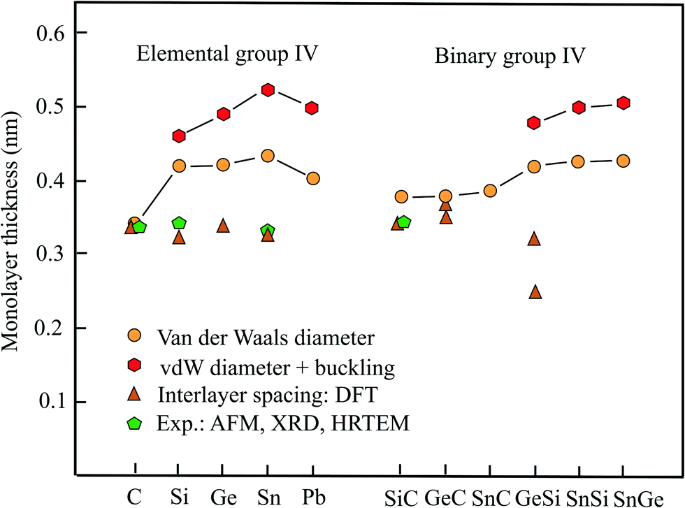 | ||
| Fig. 1 Monolayer thickness values approximated by the vdW diameter, the sum of vdW diameter and buckling effect, as well as measured and calculated interlayer spacing of elemental and binary group-IV compounds. | ||
AFM measurements on silicene monolayers prepared by the liquid-phase method resulted in a thickness of 0.6 nm.18 Measurements of the interlayer distance of few-layer silicene nanosheets by HRTEM and selected area electron diffraction (SAED) resulted in an interlayer spacing of only 0.34 nm.18 In comparison with the latter thickness, which is comparable to that of graphene, the vdW diameter of 0.420 nm yields a value of 0.461 nm, if the buckling effect of 0.041 nm is included. It should be mentioned that by a first-principles study a much lower interlayer distance of 0.312 nm was found for the lowest energy configuration of the buckled bilayer.19 Owing to buckling the symmetry of silicene is reduced to the space group Pm1.20 Remarkably, under tension, the interlayer distance of the bilayer decreases further, because the interlayer interaction is intensified by covalent σ bonds and the resulting interlayer distance approaches the intralayer bond length of 0.241 nm of the honeycomb network.21
Unfortunately, no measurements of the interlayer spacing are available for germanene multilayers. The already discussed first-principles study on optimized stacking of bilayers reports an interlayer spacing of 0.335 nm for buckled germanene.19 This small interlayer distance is consistent with the large interlayer interaction energy of −300 meV per atom calculated for germanene.22 Similar to silicene, a flat phase with the same interlayer and intralayer bond length of 0.241 nm of the bilayer is energetically more stable than its stacked buckled phase.21 The monolayer thickness estimated by adding the vdW diameter of 0.422 nm and buckling effect of 0.068 nm16 amounts to 0.490 nm.
By AFM experiments a similar thickness of 0.33 nm has been measured for stanene,23 in surprisingly good agreement with the presented first-principles-based DFT calculation of 0.326 nm for free-standing stanene.24 As discussed before, the buckled bilayer of stanene can also be converted to the stable flat phase with a reduced interlayer separation that essentially agrees with the intralayer bond length of 0.294 nm.21 Contrary to these values, a much larger thickness of 0.546 nm has been proposed for the buckled monolayer.25 This value is consistent with the thickness of 0.524 nm obtained with the vdW diameter of 0.434 nm and the buckling distance of 0.090 nm.16
Plumbene, as the heaviest element of the group has found attention only recently as a potential giant-gap spin Hall insulator. In the first study by MD a buckling effect of 0.071 nm has been simulated.26 However, also a larger buckling height of 0.093 nm has been suggested that is comparable to the stanene value.27 By adding this value to the vdW diameter of 0.404 nm a thickness of 0.497 nm is obtained for the corrugated plumbene layer.
The geometrical slab volume applied by adding the buckling effect to the vdW diameter delivers a larger volume than the real electron density-based volume of the corrugated monolayer. Therefore, the corresponding thickness presents an upper limit of this quantity. The corrugation effect increases the effective volume, however, not so much as assumed by the simple geometrical slab model. To gain further information on the error involved in the suggested procedure a quantitative estimate of the effective thickness of the real volume of corrugated monolayers is crucial.
Inspection of Fig. 1 reveals large deviations between the thickness derived from the spacing of bi- and multi-layers of elemental group-IV compounds and the vdW diameter, with graphene as exception. As mentioned already, the interlayer interaction is weak for graphene, while the increasing contribution of sp3 hybrids for the other homologues causes buckling of the 2D sheets that finally leads to 3D covalent bonding of the whole layered network. Experiments approved the calculated low interlayer distances reported for such layered systems. Thus, the reason why these interlayer distances are not suitable to estimate the thickness of free-standing monolayers is partial covalent interlayer bonding. The sudden expansion of the orbital size and thus thickness of silicene and its followers, in comparison to graphene, causes an increasing weakening of π bonding between pz orbitals in comparison to graphene.
Consequently, the interlayer spacing may not be suitable to calculate mechanical properties of monolayers in the case of 2D-Xenes. Nonetheless, the established Griffith's rule for the fracture strength of σ ≈ E/9,13 where σ is the ultimate strength and E the Young's modulus, has been questioned for stanene by using 0.326 nm as thickness.24 Conversely, independent DFT calculations of the Young's modulus and ultimate strength confirm the rule. The reason for this inconsistency could be the too small thickness used by the authors that is much smaller than the value of 0.524 nm suggested here (see Table 1).
2.2 Thickness of binary group-IV monolayers
From the class of binary group-IV monolayers we consider here the three plane sp2-bonded compounds SiC, GeC, and SnC and the three buckled compounds GeSi, SnSi, and SnGe. They have found interest owing to promising applications in optoelectronics, based on the capability of indirect-to-direct bandgap transitions, in going from multilayer to monolayer systems.28,29Table 1 presents the geometry or space group, vdW diameter, buckling height, theoretical method, and multilayer data, while Fig. 1 offers a comparison of vdW diameters with the calculated interlayer spacings of the binary group-IV compounds. As vdW diameter of the binary compounds the sum of the vdW radii of the two constituents is employed. Therefore, the corresponding thicknesses are in the same range as those of the elements (see Table 1).The interlayer spacing of hexagonal SiC multilayers of 0.347 nm has been measured by combining XRD and HRTEM.30 This experimental value agrees well with the results of independent first-principles calculations of 0.340 nm,19 and 0.338 nm.31 The bilayer interaction energy of −156 meV per atom (trilayer: −224 meV per atom) for AA stacking (similar values for AB stacking) indicates the formation of 2D allotropes with an effective charge on the outer bilayer.31 Note that these interlayer interaction energies are surprisingly large as will be pointed out in the discussion below. The space group of the planar SiC monolayer is Pm2.15
For GeC a similar interlayer spacing of 0.369 nm was found for the energetically preferred bilayer structure.32 A somewhat smaller interlayer distance of 0.350 nm for AB stacking of GeC has been reported in a previous publication.19 By using the first-principles pseudopotential method, for buckled GeSi an interlayer spacing of 0.323 nm has been reported for AB stacking.19 For this configuration DFT calculations with CA parametrization yield a covalently bonded bilayer structure with an interlayer separation of only 0.249 nm and a binding energy of −240 meV per atom.33
As shown in Fig. 1, for planar SiC and GeC the spacing is slightly smaller than the vdW diameter owing to electrostatic interaction. In the case of siligene (GeSi), buckling causes a larger difference. This finding of a smaller spacing can be rationalized by the relatively large interlayer binding energy, which is about a factor of three larger than the value proposed for vdW interaction in graphite.33 For the other buckled compounds, no information on the interlayer separation and binding energy could be found.
The vdW diameter agrees reasonable-well with both the experimental and theoretical interlayer separations of SiC and GeC. The assumption of a modest enforcement of vdW interaction is consistent with the interlayer interaction energies of SiC bilayers, which vary between −34 and −55 meV per atom, depending on stacking.34 Contrary to this situation stronger covalent-type interlayer bonding and therefore larger deviations are found for buckled GeSi.33 Obviously, the tabulated vdW radii allow a reasonable estimate of the monolayer thickness only for the weakly interacting plane binary group-IV compounds.
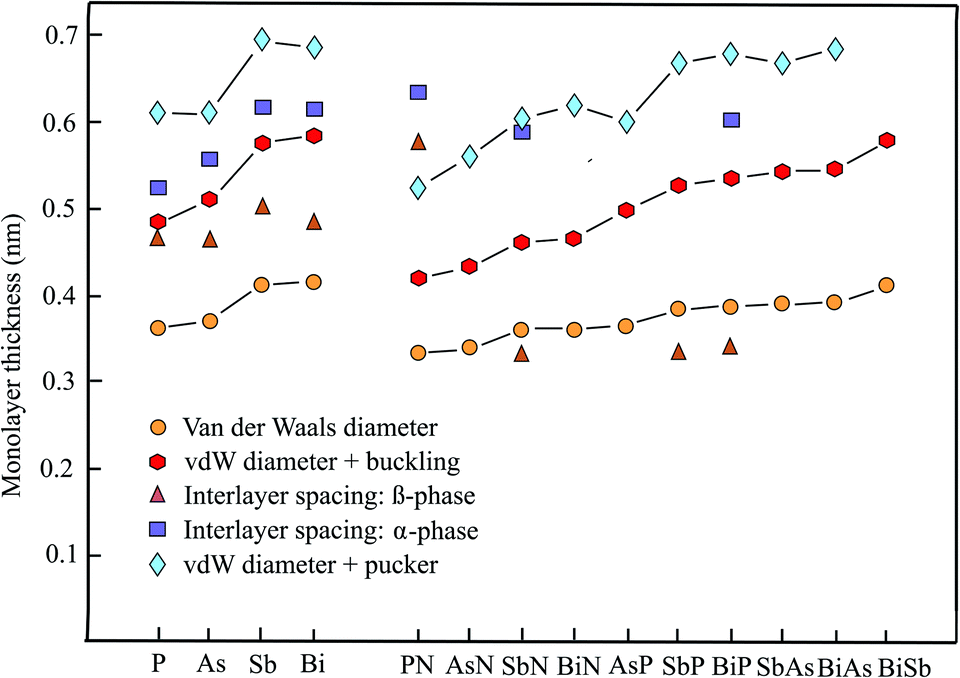
2.3 Thickness of elemental group-V monolayers
The enormous progress achieved recently in experimental and theoretical investigations of the hexagonal elemental group-V monolayers phosphorene, arsenene, antimonene, and bismuthene and their potential applications in electronics, optoelectronics, thermoelectrics, and topological spintronics have been discussed in a comprehensive review.35 Phosphorene has already been manufactured by exfoliating black phosphorus with a first measurement of the thickness by AFM of ∼0.85 nm (theory 0.616 nm),36 while monolayers of antimony, arsenic, and bismuth could be prepared by bottom-up growth on various surfaces under ultrahigh vacuum (UHV) conditions. Free-standing few-layer films of arsenene could be isolated by the adhesive tape method and those of antimonene by ultrasonication.37Table 2 presents the geometry or space group, vdW diameter, corrugation, thickness values, theoretical methods, and information on bi- and few-layer systems. Fig. 2 shows the results for the monolayer thickness and interlayer spacing, including the corrugation effects.| Geometry space group | vdW diam. dw (nm) | Buck., pucker Δz (nm) | Thickness dw + Δz (nm) | Method monolayer | Inter. spacing dsp (nm) | Inter. binding (meV per atom) | |
|---|---|---|---|---|---|---|---|
| Phosphorene | hex., buckl.41 | 0.36014 | 0.12441 (β) | 0.484 (β) | DFT-PBE41 | 0.40941 (β) | −642 |
| Pmna 59 | 0.25139 (α) | 0.611 (α) | DFT-PBE39 | 0.52440 (α) | −2036 | ||
| Arsenene |
Pm145 |
0.37014 | 0.14043 (β) | 0.510 (β) | DFT-PBE43 | 0.46743 (β) | −30,44 −89.648 |
| Pmna 45,59 | 0.23943 (α) | 0.609 (α) | DFT-PBE43 | 0.55444 (α) | −5344 | ||
| Antimonene | hex., buckl.41 | 0.41214 | 0.16541 (β) | 0.577 (β) | First princip.41 | 0.50237 (β) | −124,38 −86.048 |
| Pmna 59 | 0.28239 (α) | 0.694 (α) | DFT-PBE39 | 0.61638 (α) | −6838 | ||
| Bismuthene | hex., buckl.41 | 0.41414 | 0.17141 (β) | 0.585 (β) | First princip.41 | 0.48046 (β) | −136,46 −12347 |
| Pmna 59 | 0.27239 (α) | 0.686 (α) | DFT-PBE39 | 0.61246 (α) | −12046 | ||
| PN | P3m156 | 0.33514 | 0.08649 (β) | 0.421 (β) | DFT-PBE49 | 0.57653 (β) | — |
| Pmn2156 | 0.19049 (α) | 0.525 (α) | DFT-PBE49 | 0.63553 (α) | |||
| AsN | P3m156 | 0.34014 | 0.09756 (β) | 0.436 (β) | DFT-PBE56 | — | — |
| Pmn2156 | 0.22156 (α) | 0.561 (α) | DFT-PBE56 | ||||
| SbN | P3m156 | 0.36114 | 0.10256 (β) | 0.462 (β) | DFT-PBE56 | 0.33255 (β) | — |
| Pmn2156 | 0.24356 (α) | 0.603 (α) | DFT-PBE56 | 0.59054 (α) | |||
| BiN | P3m156 | 0.36214 | 0.10556 (β) | 0.467 (β) | DFT-PBE56 | — | — |
| Pmn2156 | 0.25956 (α) | 0.621 (α) | DFT-PBE56 | ||||
| AsP | P3m150 | 0.36514 | 0.13249 (β) | 0.497 (β) | DFT-PBE49 | — | — |
| Pmn2159 | 0.23549 (α) | 0.600 (α) | DFT-PBE49 | ||||
| SbP | P3m150 | 0.38614 | 0.14149 (β) | 0.527 (β) | DFT-PBE49 | 0.33455 (β) | — |
| Pmn2159 | 0.28549 (α) | 0.671 (α) | DFT-PBE49 | ||||
| BiP | hex., buckl.58 | 0.38714 | 0.14858 (β) | 0.535 (β) | First princip.58 | 0.34255 (β) | — |
| Pmn2159 | 0.29350 (α) | 0.680 (α) | DFT-PBE50 | 0.60654 (α) | |||
| SbAs | P3m150 | 0.39114 | 0.15249 (β) | 0.543 (β) | DFT-PBE49 | — | — |
| Pmn2159 | 0.28049 (α) | 0.671 (α) | DFT-PBE49 | ||||
| BiAs | P3m150 | 0.39214 | 0.15550 (β) | 0.548 (β) | DFT-PBE50 | — | — |
| Pmn2159 | 0.29550 (α) | 0.687 (α) | DFT-PBE50 | ||||
| BiSb | P3m150 | 0.41314 | 0.16950 (β) | 0.582 (β) | DFT-PBE50 | — | — |
| Pmn2159 | 0.33550 (α) | 0.748 (α) | DFT-PBE50 | ||||
 | ||
| Fig. 2 Monolayer thickness values approximated by the vdW diameter, the sum of vdW diameter and buckling or puckering effect, as well as calculated interlayer spacing of elemental and binary group-V compounds. | ||
The pnictogen monolayers exist in two stable phases, which may have nearly the same stability, the puckered α-phase (washboard or w-phase) realized in orthorhombic black phosphorus and the buckled β-phase (b-phase) realized in blue phosphorus, usually holding the minimum energy configuration. The term buckling is used here for a small zigzag-like corrugation that can be characterized by one lattice constant and one bond length, whereas the pucker effect (symmetric or antisymmetric) designates a washboard-like corrugation that must be described by two lattice constants and two bond lengths.
Contradicting results on the most stable phase, sometimes found in the literature, are due to the small difference in the cohesive energy. For example, while puckered antimonene has the minimum energy configuration, the cohesive energy of buckled antimonene is close and β-Sb is more stable than α-Sb in multilayers with more than 3 layers.38
The interest in anisotropic puckered phosphorene arises from its direct band gap and the high carrier mobility. By adding the large puckering height of 0.251 nm to the vdW diameter of 0.360 nm we find a layer thickness of 0.611 nm for the most stable α-phase.39 This value can be compared with an independent estimate of 0.524 nm, based on the nearest layer distance of adjoined layers in a multilayer of 0.307 nm and a smaller pucker effect of 0.217 nm.40 Interestingly, the interlayer interaction energy of the α-phase with AB stacking is only −20 meV per atom.36 A much smaller interlayer spacing of 0.412 nm has been determined for the bulk β-phase using 0.288 nm for the nearest interlayer distance of adjoined layers and 0.124 nm for buckling.41 However, based on ab initio calculations, also a larger interlayer spacing of 0.563 nm has been reported for the buckled β-phase of blue phosphorus.42 Similar to the results for the actual stacking configuration (AB) of the α-phase an extremely low interlayer interaction energy of −6 meV per atom has been reported for the β-phase.42
The wide band gap, which changes from indirect to direct by applying strain or an external field, stimulated the first-principles calculations performed recently for arsenene and its multilayers. For the most stable buckled lattice of β-As the following bulk and tri-layer interlayer spacings of 0.455 nm,37 0.536 nm (AB),41 and 0.450 nm (AAA)43 have been evaluated by adding the buckling effect of 0.140 nm to the reported nearest interlayer distances between atoms of adjacent layers.43 Note that for the bilayer of β-As an interlayer spacing of 0.467 nm has been reported.43 With the vdW diameter of 0.370 nm and the buckling effect of 0.140 nm a formal monolayer thickness of 0.510 nm for β-As and with the pucker height of 0.239 nm43 a thickness of 0.609 nm for α-As is derived. A systematic investigation of the nearest interlayer distances of bilayers by diffusion quantum Monte Carlo (DMC) and DFT calculations resulted in 0.352 nm for β-As (AA) and 0.315 nm for α-As (AB), resulting in layer spacings of 0.455 nm and 0.554 nm, respectively.44 A smaller interlayer interaction energy of -30 meV per atom (AA) has been calculated for β-As than for α-As at −53 meV per atom (AB) by the DMC method.44 For buckled arsenene the space group is Pm1 and for the puckered configuration it is Pmma.45
Like arsenene, antimonene is of interest due to its semiconducting properties and its wide band gap. For the buckled phase (β-Sb) an interlayer spacing of multilayers of only 0.365 nm (AB), with a bilayer interaction energy of −124 meV per atom, and for the puckered phase (α-Sb) a much larger spacing of 0.616 nm (AB), with a smaller bilayer binding energy of −68 meV per atom, have been reported.38 For comparison, an interlayer spacing of 0.448 nm (AB) has been calculated for the bulk rhombohedral honeycomb lattice of β-Sb.41 Furthermore, an even larger interlayer spacing of 0.502 nm has been reported for the bulk β-phase of antimonene by an independent study.37 With the buckling effect of 0.165 nm41 and the vdW diameter of 0.412 nm a monolayer thickness of 0.577 nm can be extracted for the β-phase. Accordingly, the wide pucker height of 0.282 nm39 causes a larger thickness of 0.694 nm for the α-phase.
The honeycomb monolayer of the heaviest group-V element bismuthene has just recently attracted interest as a room-temperature TI, showing great promise for spintronic applications. Bismuthene is a narrow band gap semiconductor. First-principles DFT-PBE calculations for multilayer β-bismuthene delivered a bulk interlayer spacing of 0.442 nm (AB), including a buckling effect of 0.171 nm.41 The interlayer distances between nearest atoms in bilayer β-Bi (AA) at 0.309 nm and α-Bi (AA) at 0.340 nm result in interlayer spacings of 0.480 nm and 0.612 nm, using the buckling effect of 0.171 nm and a pucker height of 0.272 nm,39 respectively.46 For β-Bi (AA) stacking an interlayer binding energy of −123 meV per atom has been obtained, by employing the DFT-PBE approximation without SOC and −170 meV per atom with SOC.47 With the buckling effect of 0.171 nm and the vdW diameter of 0.414 nm a monolayer thickness of 0.585 nm can be extracted for the β-phase and with the pucker effect of 0.272 nm a thickness of 0.686 nm is obtained.
The interlayer separations of α-phase and β-phase bilayers and multilayers of pnictogens have been determined by a series of first-principles methods. As can extracted from the discussion presented above, the corresponding interlayer spacing of phosphorene, arsenene, antimonene, and bismuthene scatter around thickness values which are lower than those defined by the vdW diameter and the combination of vdW diameter and corrugation effect. While the effect of an increasing number of layers on the interlayer spacing is not negligible going from a bilayer to multilayers, the stacking order also can change the interlayer spacing substantially and therefore is shown together with the spacing.
To select the best stacking configuration for an eventual evaluation of the isolated monolayer thickness, it is useful to consider the invers behavior between interlayer spacing and interlayer binding energy. For both α-P and β-P AB stacking leads to small interlayer binding energies of −20 meV per atom36 and −6 meV per atom.42 Therefore, a reasonable agreement between the calculated spacing and the vdW-diameter-based thickness could be envisaged for phosphorene. For arsenene and antimonene DFT calculations delivered comparable interlayer interaction energies of −89.6 meV per atom and −86.0 meV per atom, respectively.48 However, also substantially smaller values of −30 meV per atom (β-As) and −53 meV per atom (α-As) have been suggested, indicating the difficulties encountered in the determination of accurate interaction energies. Since these values are on the upper limit of vdW interaction still useful thicknesses may result from the interlayer separations. According to the larger bilayer binding energies of −124 meV per atom (β-Sb) and −68 meV per atom (α-Sb)38 and of −123 meV per atom (DFT-PBE) and −170 meV per atom (DFT-PBE + SOC) for β-Bi larger deviations are expected.47
Altogether, the presented results are consistent with the assumption that primarily the interlayer interaction energy controls the suitability of calculated and measured interlayer distances and spacings for a realistic prediction of free monolayer thicknesses. Whenever sp3-like hybrids contribute to interlayer bonding or interaction with a surface, covalent forces diminish the thickness of a free monolayer with a conforming change of the multilayer properties. Interestingly, quasi-free-standing monolayers of heavier elements could be realized by adding a suitable buffer layer between surface and monolayer.
2.4 Thickness of binary group-V monolayers
First-principles investigations of binary group-V monolayers are finding increasing attention, driven by the search for ferroelectric materials, TIs, and dissipationless transport devices. While theoretical studies predict stable binary honeycomb semiconductors with direct and indirect band gaps the experimental verification of these predictions is still widely lacking. For the stable phases of binary group-V compounds both the α-phase and β-phase configurations will be considered (see Table 2).49–53 This includes the compounds PN, AsN, SbN, BiN, AsP, SbP, BiP, SbAs, BiAs, and BiSb. Unfortunately, detailed information on the corresponding structural properties of their multilayers is mostly absent. Fig. 2 shows the thickness values with and without corrugation and available interlayer spacings of α-phase and β-phase compounds.Using first-principles calculations, a stable puckered monolayer of α-PN and a stable buckled monolayers of β-PN have been predicted (note that the nomenclature of the authors has been changed).53 By adding the buckling effect of 0.086 nm49 to the nearest layer distances of 0.490 nm (AA) and 0.541 nm (AB) of layered β-PN, interlayer spacings of 0.576 nm and 0.627 nm are found.53 Even larger interlayer spacings are obtained by adding the large pucker effect of 0.190 nm49 to the nearest interlayer distances of α-PN of 0.446 nm (AA) and 0.445 nm (AB), yielding interlayer spacings of 0.636 nm (AA) and 0.635 nm (AB), respectively.53 By adding the buckling effect of 0.086 nm and pucker height of 0.190 nm to the sum of the vdW radii of the two constituents a vdW diameter of 0.335 nm and layer thicknesses of 0.421 nm (β-PN) and 0.525 nm (α-PN) are found.
Ab initio calculations of the bulk interlayer spacing of α-SbN at 0.590 nm and α-BiP at 0.606 nm were based on the α-structure of phosphorene and the most stable AA stacking order, where the second layer directly stacks on the first layer with no rotation or translation.54 Note that significantly lower interlayer spacings have been evaluated for ABC stacking of the bulk rhombohedral crystals of β-SbN (0.332 nm), β-SbP (0.334 nm), and β-BiP (0.342 nm) in their ground state structure.55 The sum of the vdW radii of these and the other binary compounds, as well as the inclusion of their buckling and pucker effects, are displayed in Table 2.
Additional data on buckling and puckering has been taken from a study on nitride compounds with auxiticity.56 Moreover, from studies on strain induced QSH insulator behavior of β-BiSb and strain induced topological phase transitions in binary bismuth compounds.57,58 Finally, important information on the relevance of the layer thickness on thermal transport properties has been published.59 The present status of both theory and experiments of 2D V–V binary materials has been reviewed.60
Inspection of Fig. 2 shows that the sum of the vdW radii increases continuously from 0.335 nm for PN to 0.413 nm for BiSb. This slight increase of the vdW diameters with atomic number arises from the increase of the orbital size within the chemically related group members of the periodic table. The buckling effects enlarge the vdW thicknesses, especially in the case of the heavier compounds. Since both the vdW diameters and buckling effects are well-established by independent studies, the interlayer spacings of β-SbN, β-SbP, and β-BiP are much smaller than the monolayer thicknesses. Owing to the increased contribution of sp3 hybrids strong bonding takes place between the layers of nitrides and phosphates.55 It is not clear yet, why the interlayer spacing of β-PN is much larger than expected. The few interlayer spacings available for the puckered compounds α-PN, α-SbN, and α-BiP are in qualitative agreement with the layer thicknesses resulting from the sum of vdW diameter and pucker effect, despite large scatter.
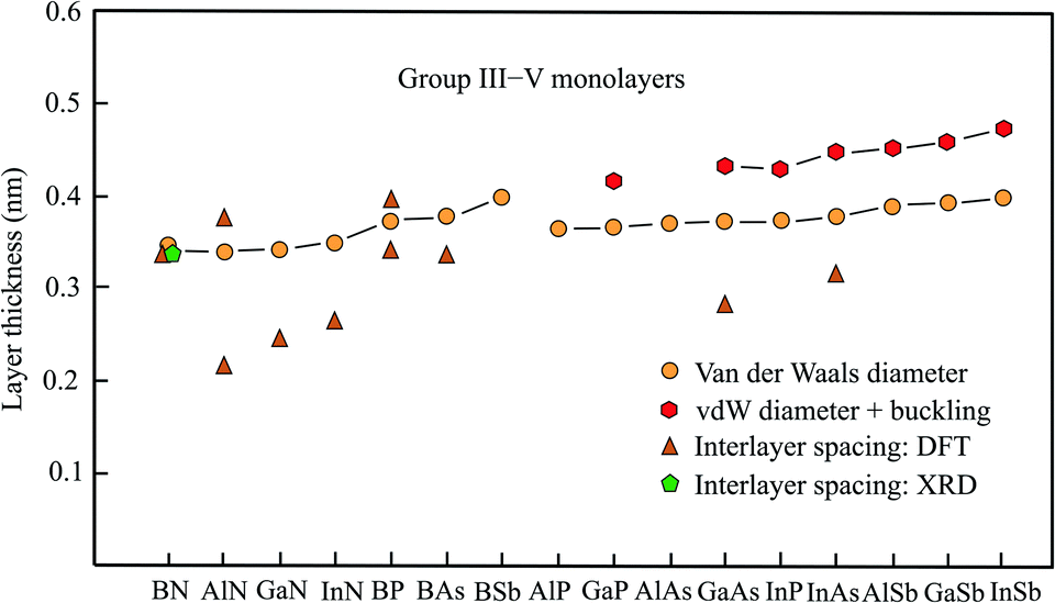
2.5 Thickness of group III–V monolayers
The semiconducting members of group III–V compounds are of interest owing to their large band gaps and piezoelectric properties. The following compounds with an atom of the second row of the periodic table have a planar honeycomb structure (BN, BP, BAs, BSb, AlN, GaN, InN). The other compounds achieve their stable hexagonal structure by buckling in the vertical direction (AlSb, GaP, GaAs, GaSb, InP, InAs, InSb).61 The buckling effects presented in Table 3, taken from the most comprehensive work,61 are in good agreement with those of other publications.62,63 The data available for this group, including the space groups,64 is collected in Table 3. Fig. 3 shows the interlayer spacings and monolayer thicknesses derived with the vdW diameter.| Geometry space group | vdW diam. dw (nm) | Buckling Δz (nm) | Thickness dw + Δz (nm) | Method monolayer | Int. spacing dsp (nm) | Inter. binding (meV per atom) | |
|---|---|---|---|---|---|---|---|
| h-BN |
Pm264 |
0.34714 | 061 | 0.347 | DFT-PBE61 | 0.33365 | −(26–86)9,10 |
| h-AlN | P4/nmm64 | 0.33914 | 061 | 0.339 | DFT-PBE61 | 0.21369 | −125,69 −29270 |
| h-GaN |
Pm264 |
0.34214 | 061 | 0.342 | DFT-PBE61 | 0.24771 | −140,72 −29071 |
| h-InN |
Pm264 |
0.34814 | 061 | 0.348 | DFT-PBE61 | 0.26773 | — |
| h-TlN |
Pm175 |
0.35114 | 0.02974 | 0.380 | DFT-PBE74 | 0.25175 | −18575 |
| BP |
Pm264 |
0.37214 | 061 | 0.372 | DFT-PBE61 | 0.33976 | −112,76 −13476 |
| BAs |
Pm264 |
0.37714 | 061 | 0.377 | DFT-PBE61 | 0.33577 | — |
| BSb |
Pm264 |
0.39814 | 061 | 0.398 | DFT-PBE61 | — | — |
| AlP | Pmn2164 | 0.36414 | 061 | 0.364 | DFT-PBE61 | — | — |
| AlAs | P4/nmm64 | 0.37914 | 061 | 0.369 | DFT-PBE61 | — | — |
| GaP | Pmn2164 | 0.36714 | 0.04861 | 0.415 | DFT-PBE61 | — | — |
| GaAs | Pmn2164 | 0.37214 | 0.06161 | 0.433 | DFT-PBE61 | 0.28377 | — |
| InP | Pmn2164 | 0.37314 | 0.05661 | 0.429 | DFT-PBE61 | — | — |
| InAs | Pmn2164 | 0.37814 | 0.07161 | 0.449 | DFT-PBE61 | 0.31577 | — |
| AlSb | P4/nmm64 | 0.39014 | 0.06261 | 0.452 | DFT-PBE61 | — | — |
| GaSb | Pmn2164 | 0.39314 | 0.06861 | 0.461 | DFT-PBE61 | — | — |
| InSb | Pmn2164 | 0.39914 | 0.07761 | 0.476 | DFT-PBE61 | — | — |
| TlP |
Pm175 |
0.37614 | 0.06674 | 0.442 | DFT-PBE74 | 0.28075 | −9175 |
| TlAs |
Pm175 |
0.38114 | 0.07474 | 0.455 | DFT-PBE74 | 0.28775 | −7975 |
| TlSb |
Pm175 |
0.40214 | 0.08274 | 0.484 | DFT-PBE74 | 0.303 | −7675 |
 | ||
| Fig. 3 Monolayer thickness values approximated by the vdW diameter, the sum of vdW diameter and buckling, as well as measured and calculated interlayer spacing of group III–V compounds. | ||
Boronitrene currently belongs to the best studied monolayers. The monolayer thickness of 0.333 nm, derived from interlayer spacing, agrees surprisingly well with that of graphite, despite the expected contribution of electrostatic interlayer forces.65 Already early X-ray studies of boron nitride attained an interlayer spacing of 0.333 nm.66 This has been confirmed by the layer spacing of 0.33 nm obtained by recent XRD measurements on 50 nm thick h-BN films, synthesized by ambient pressure CVD.67 In excellent agreement with these results are detailed calculations of the binding energy, also predicting an interlayer distance of 0.333 nm and interlayer interaction energies of −26 to −86 meV per atom from bilayer to multilayer.9,10,68 An estimation of the thickness by the vdW diameter using the sum of van der Waals radii of the boron atom (0.192 nm) and nitrogen atom (0.155 nm) yields 0.347 nm.14 The small deviation suggests that the sum of vdW radii provides a useful description of the size of planar binary compounds.
Besides h-BN few-layer systems of the group-III nitrides h-AlN and h-GaN have received most attention due to their semiconducting properties with a wide band gap. Contrary to the space group given in Table 3, the space group P63/mmc has been assumed for h-AlN.69 The stacking orders with the smallest interlayer interaction energy offer the most realistic estimate of the thickness of an isolated monolayer. Clearly, in the considered compounds interlayer anion–cation interaction enlarges the inherent bonding by vdW forces. For AA′ stacking with the largest interlayer coupling energy of highly polar h-AlN the bilayer distance is only 0.213 nm. This is due to the interlayer interaction energy of −125 meV per atom for AA′ stacking (Al over N and N over Al).69 Independently, a similar interlayer distance of 0.218 nm and a bilayer interaction energy of −292 meV per atom have been calculated for the ground-state configuration.70 For AA stacking (Al over Al and N over N) the interlayer spacing increases to 0.376 nm and the binding energy decreases to −32 meV per atom (see Table 3).70
Optimum stacking AA′AA′… (i.e. hexagons on top of each other with Ga above N) of bilayer, trilayer, and multilayer h-GaN aggregates also exhibits large interlayer interaction energies of −142 meV per atom, −200 meV per atom, and −327 meV per atom, respectively.5 Surprisingly, the authors argue that interlayer interaction is dominated by van der Waals forces despite the small interlayer separations of 0.252 nm and 0.249 nm for bi- and tri-layers, respectively. Only in multilayers with 0.244 nm separation a slight chemical contribution from anion–cation interaction is proposed.5 In a study based on vdW-DFT calculations a similar interlayer distance of 0.247 nm but −290 meV per atom for the interaction energy of AA′ stacked bilayers has been obtained.71 DFT-PBE calculations confirmed both the small interlayer separation of 0.247 nm and the large interlayer binding energy of −140 meV per atom.72 Conversely, these authors consider the electrostatic interaction of Ga (N) and N (Ga) between the layers as main contribution.
Likewise, small interlayer separations of 0.267 nm, 0.266 nm, and 0.256 nm for the bi-, tri-, and four-layer systems of h-InN have been found, owing to the substantial difference in electronegativity. This again confirms the strong effect of ionicity on the effective interlayer spacings of nitrides and consequently on their electronic properties.73 As described before, the sum of the tabulated vdW radii was employed to estimate the quite similar vdW diameters of h-AlN (0.339 nm), h-GaN (0.340 nm), and h-InN (0.348 nm), which are comparable with that of h-BN.14 Thus, the real monolayer thickness is substantially larger than the interlayer spacing derived for few-layer systems of nitrides with strong ionic layer-by-layer interaction.
On the search for 2D TIs a new family of thallium compounds h-TlA (A = N, P, As, and Sb) has been discovered.74 The geometric structures were calculated by first principles and simulated by MD, yielding slightly buckled hexagonal structures, including the nitride h-TlN, as shown in Table 3. The resulting thickness values of dw + Δz = 0.38 nm (TlN), dw + Δz = 0.442 nm (TlP), dw + Δz = 0.455 nm (TlAs), and dw + Δz = 0.484 nm (TlSb) are consistent with those of the related compounds presented in Table 3, with the exception that TlN is no longer planar. The general picture, however, noticed for bilayers of this group agrees with the behavior of the other nitrides. The bilayer of TlN has the smallest interlayer spacing of 0.251 nm and strongest interlayer interaction of −185 meV per atom followed by TlP (0.280 nm, −91 meV per atom), TlAs (0.287 nm, −79 meV per atom), and TlSb (0.303 nm, −76 meV per atom).75
Boron-phosphide (BP) has attracted recent interest owing to its flat honeycomb monolayer with direct band gap. For the most stable configuration of bilayers with AB stacking and direct band gap the interlayer interaction energy is −134 meV per atom and for the most unfavorable AA stacking it is −112 meV per atom.76 Accordingly, a larger interlayer spacing of 0.393 nm was found for AA stacking and only 0.339 nm for AB stacking approaching the vdW diameter (see Table 3). For tri- and four-layer systems the interlayer interaction energy increases slightly to −152 (ABC) and −161 meV per atom (ABCA), respectively.76
First-principles calculations have also been performed for the most stable few-layer systems of planar BAs (AC), buckled GaAs (AB), and buckled InAs (AB).77 These calculations delivered the following interlayer spacings of bilayers of 0.335 nm (BAs), 0.283 nm (GaAs), and 0.315 nm (InAs), which are partly smaller than the trilayer spacings of 0.339 nm (BAs), 0.326 nm (GaAs), and 0.315 nm (InAs). The buckling effects of 0.086 nm (GaAs) and 0.088 nm (InAs), presented by these authors, are slightly larger than those given in Table 3. For bilayer GaN the authors present an interlayer spacing of 0.252 nm consistent with the value listed in Table 3.
Inspection of Fig. 3 demonstrates agreement between the experimental interlayer spacing, theoretical interlayer spacing, and vdW diameter only for h-BN, whereas the few available first-principles calculations of bilayer and few-layer spacings of the other nitrides deviate considerably from the mean vdW diameter. One reason for the short interlayer distances is the strong ionic interlayer interaction, as discussed for h-AlN and h-GaN.5,69,72 In such cases of strong electrostatic interaction of bilayers their separation is no longer suitable to assess the free-standing monolayer thickness. In h-GaN bilayers, for example, the N atoms are positioned exactly above Ga atoms in the most stable stacking configuration with 0.244 nm spacing.5
Only in very few cases, stacking configurations exist, where the interlayer spacing approaches the vdW diameter. This situation is encountered for BP, where the spacing of the weak bonding configuration approaches the vdW-based thickness (see Fig. 3).75 The absence of charge transfer between the AA-stacked layers produces a relatively weak interlayer interaction, leading to the good agreement between interlayer distance and vdW-based monolayer thickness. The varying agreement between interlayer spacing and monolayer thickness found for the group-III arsenides also reflects the strength of interlayer bonding. The realization of π–π bonding by overlapping pz orbitals in planar sp2 geometry of BAs changes to buckled GaAs and InAs with dominant sp3-type bonding due to increasing mixing of pz and s orbitals.
The results collected for this group of III–V compounds undoubtedly reveal the reduction of interlayer spacing caused by strong electrostatic interactions in planar few-layer III–V sheets. In the buckled systems, covalent interlayer interaction takes place by mixed hybridization and efficient stacking orders. It is important to note that these types of stronger interlayer interaction of monolayers likewise occur on surfaces.
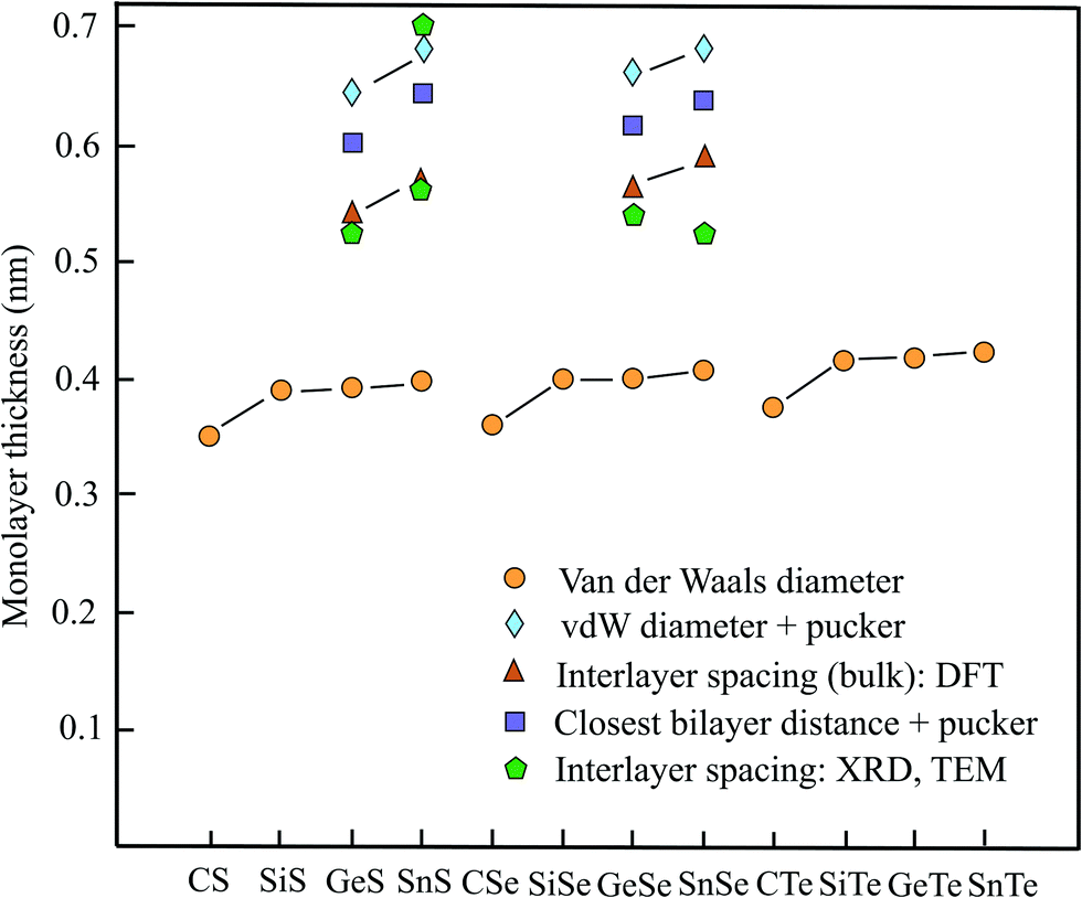
2.6 Thickness of group IV–VI monolayers
In analogy to the already discussed III–V compounds binary group IV–VI compounds or group-IV monochalcogenides are the isoelectronic counterparts of elemental group-V semiconductors such as phosphorene. Different to phosphorene the monolayers exhibit SOC since inversion symmetry is missing. Some members of this group of binary monolayers MX (M = C, Si, Ge, Sn and X = S, Se, Te) have found increasing attention, owing to their high carrier mobility, low thermal conductivity, enhanced piezoelectricity, chemical stability, and strong absorbance of visible light. Therefore, they are candidates for future applications in electronics, optoelectronics, and photovoltaics. The MTe compounds with the vdW diameters of 0.376 nm (CTe), 0.416 nm (SiTe), 0.417 nm (GeTe), and 0.423 nm (SnTe) are not presented in Table 4, however, they are included in Fig. 4.14| Geometry space group | vdW diam. dw (nm) | Near. dist. dn (nm) | Pucker Δz (nm) | Thickness dw or dn + Δz | Method monolayer | Spacing dsp (nm) | Inter. binding (meV per atom) | |
|---|---|---|---|---|---|---|---|---|
| CS | Pmn2185 | 0.35014 | — | — | — | — | — | — |
| SiS | Pmn2185 | 0.39014 | — | — | — | — | — | — |
| GeS | Pmn2185 | 0.39114 | — | 0.25684 | 0.64714,84 | DFT-PBE84 | 0.54178 | — |
| — | 0.34682 | 0.25684 | 0.60282,84 | DFT-PBE82 | 0.52481 | — | ||
| SnS | Pmn2185 | 0.39714 | — | 0.28584 | 0.68214,84 | DFT-PBE84 | 0.56978 | — |
| — | 0.36082 | 0.28584 | 0.64582,84 | DFT-PBE82 | 0.56081 | — | ||
| CSe | Pmn2185 | 0.36014 | — | — | — | — | — | — |
| SiSe | Pmn2185 | 0.40014 | — | — | — | — | — | — |
| GeSe | Pmn2185 | 0.40114 | — | 0.26284 | 0.66314,84 | DFT-PBE84 | 0.56678 | −37.583 |
| — | 0.35282 | 0.26284 | 0.61482,84 | DFT-PBE82 | 0.54181 | −52.383 | ||
| SnSe | Pmn2185 | 0.40714 | — | 0.27584 | 0.68214,84 | DFT-PBE84 | 0.59178 | −11087 |
| — | 0.36382 | 0.27584 | 0.63882,84 | DFT-PBE82 | 0.52581 | −14686 |
 | ||
| Fig. 4 Monolayer thickness values approximated by the vdW diameter, the sum of vdW diameter or nearest layer distance and puckering effect, as well as measured and calculated interlayer spacing of group IV–VI compounds. | ||
From the three free-standing geometrical configurations, namely planar, buckled, and puckered the slightly deformed puckered orthorhombic configuration (antisymmetric α phase) normally is the most stable structure of these compounds with the exceptions of SiS and SiSe, which have nearly the same cohesive energy for the buckled configuration. For some puckered monolayers the indirect band gap can be transformed into direct band gap because of the small difference between direct and indirect band gap. Table 4 covers the space group, vdW diameter, pucker, thickness, theoretical method, interlayer spacings, and interlayer binding for puckered compounds. Fig. 4 displays the vdW diameter, corrugated monolayer thickness, and interlayer spacing of selected group IV–VI compounds.
First-principles calculations of the bulk interlayer spacing of orthorhombic structures have been performed for GeS (0.541 nm), GeSe (0.566 nm), SnS (0.569 nm), and SnSe (0.591 nm).78 These values agree well with the thicknesses of GeS (0.56 nm), GeSe (0.54 nm), SnS (0.56 nm), and SnSe (0.57 nm) presented in a review.79 For multiple SnS layers the theoretical findings have been confirmed by HRTEM measurements, which acquired 0.56 nm, matching the DFT-based values.80 The theoretical interlayer separations, estimated from the size of the orthorhombic primitive unit cell of the bulk material, are collected in Table 4, together with the early XRD data on the orthorhombic crystals of GeS (0.524 nm), GeSe (0.541 nm), SnS (0.560), and SnSe (0.525 nm).81
The computation of the nearest interlayer distance of the atoms of adjacent layers offers an alternative approach to estimate the layer thickness. Such calculations have been performed for different stacking orders.82 For AD stacking, where the upper and under layers are the mirror image of each other (mutual location of the same atoms), the minimal interlayer interaction leads to the following nearest layer distances GeS (0.346 nm), GeSe (0.352 nm), SnS (0.360 nm), and SnSe (0.363 nm).82 With the exception of GeSe, showing slightly more stable AA stacking, the corresponding distances of the most stable AB stacking are roughly 20% lower. Independent calculations of the closest interlayer distance of adjacent atoms reported for bilayer GeSe provide a similar result of 0.33 nm for AD stacking and an interlayer binding energy of −37.5 meV per atom.83 For the most stable AA stacking of GeSe the binding energy is −52.3 meV per atom.
To find the effective layer thickness of corrugated monolayers the pucker distance is needed. This has been provided by first-principles calculations for the four compounds with the following values: GeS (0.256 nm), GeSe (0.262 nm), SnS (0.285 nm), and SnSe (0.275 nm).84 The resulting interlayer distances of GeS (0.602 nm), GeSe (0.614 nm), SnS (0.645 nm), and SnSe (0.638 nm) are compared with the ideal interlayer spacings derived from the unit cell and measured interlayer spacings in Fig. 4.
Owing to the extreme pucker effect, the layer thicknesses derived from the mean vdW diameters are far too small (see Fig. 4). As discussed before, the upper limit of the thickness of puckered monolayers can be predicted, by using the calculated pucker distances given above.84 A measurement of the monolayer thickness of SnS by cross-sectional TEM yielded ∼0.7 nm.85 Inspection of Fig. 4 shows that the pucker-vdW-diameter-based thickness is in reasonable agreement with the TEM experiment including the one estimated by the closest-layer distances. The bulk layer spacings measured by XRD are in general lower and in better agreement with the DFT calculations of the interlayer spacings, pointing to an enlargement of interlayer interaction with the number of layers.
The interlayer binding energies presented above for GeSe suggest that vdW forces are responsible for the interaction between puckered layers.83 However, a much stronger interlayer interaction of −146 meV per atom has been calculated for layered bulk SnSe by taking into account different exchange–correlation functionals and vdW interaction in a DFT-based study.85,86 These authors assume strong charge transfer between layers by lone pair electrons and expect difficulties for preparation by exfoliation methods. Different from this conclusion other authors using the DFT-PBE functionals concluded that SnSe exhibits with −110 meV per atom the limit of the interlayer interaction energy of group IV–VI compounds and considered this as still favorable for exfoliation.87
3. Discussion of thickness values
For completion, a brief discussion of recent progress made in studies of group-III monolayers is necessary. Besides boron, the information on the group III elements is at an early stage. Boron is the lightest element that can form stable covalent monolayers. Remarkably, the stability of borophene has been predicted first by theory and then has been confirmed by experiments. With its three valence electrons boron atoms form delocalized three-center, two-electron bonds involving three boron atoms. An example is the regular triangular borophene monolayer with buckled structure.88 This so-called striped borophene has been observed on a stabilizing surface by scanning tunneling microscopy (STM).89 The thickness of 0.478 nm, estimated by the vdW diameter of 0.384 nm and the buckling height of 0.094 nm, agrees well with the general behavior of other buckled compounds, as delineated in Fig. 5. Furthermore, by suitable combination of electron donors, provided by the three-center flat triangular regions, and two-center hexagonal regions acting as electron acceptors in the right proportion boron can form stable planar polymorphs consisting of hexagonal sites with holes and triangular sites (variation of boron hexagons with and without a boron atom at the center of the hexagon).90 The description of thickness by the vdW diameter is in reasonable agreement with that of other planar monolayers.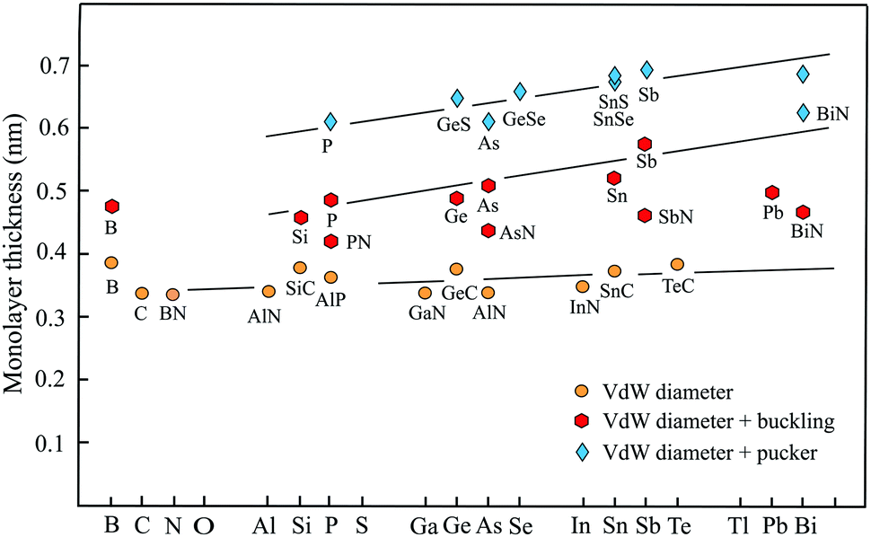 | ||
| Fig. 5 The vdW diameter-based thicknesses of planar graphene-like monolayers, buckled monolayers described by adding vdW diameter and buckling height, and puckered monolayers defined by vdW diameter and pucker effect. | ||
Fig. 5 shows the development of the thickness of group-III up to group-VI elements and compounds from period number 2 to 6 of the periodic table. We distinguish between three groups, planar monolayers with a thickness defined by the vdW diameter, buckled monolayers obtained by adding vdW diameter and buckling effect, and puckered monolayers expressed by vdW diameter plus pucker height. Note that for clarity this overview scheme encloses not all thickness values gathered in Tables 1–4.
Planar sp2 hybridization realized by atoms with four binding electrons (octet rule) and isoelectronic III–V compounds form three plane σ bonds and delocalized π–π bonds if the atoms are small enough to allow overlapping of pz orbitals. For group IV elements this is only carbon owing to the enormous increase of atom size already for silicon. Obviously, there is only one exception (TlN) from the rule that in binary III–V compounds the planar configuration is stable if one element belongs to the second period. Note that the increase of thickness from the second to the sixth period matches that of the vdW diameter, which grows only slightly from 0.34 nm to about 0.40 nm (see Fig. 5).
If the atom size is too large for an efficient overlap of the pz orbitals of group-IV elements or in the case of five valence electrons of group-V elements, the monolayer becomes buckled by the increasing influence of sp3 hybrids. Adding the buckling effect to the vdW diameter yields a first estimate of thickness. As can be seen in Fig. 5, the elemental group-IV and group-V monolayers with mixed sp2–sp3 hybridization obviously define an upper limit of thickness for buckled single-atom monolayers. Only the thickness of plumbene is much smaller than expected. The heaviest compounds often deviate from normal group behavior, which may be due to the influence of d and f electrons. The thicknesses of the corresponding binary buckled compounds are usually smaller. They appear between the line defined by the elemental buckled monolayers and the vdW diameter line (see PN, AsN, SbN, and BiN). According to Fig. 5, the thickness of buckled compounds varies in the wider range between about 0.4 nm and 0.6 nm.
With their extra bonding electron group-V elemental and their binary compounds form besides the buckled phase a puckered phase that often has a similar cohesive energy and stability. Due to the stronger corrugation the thickest monolayers belong to the puckered compounds with a thickness of about 0.5–0.7 nm. Here the strongest contribution of sp3-type bonding occurs, controlling the thickness of both the α-phase and β-phase of phosphorene, arsenene, antimonene, and bismuthene. Note that the formal increase of the layer thickness from period to period due to the pucker effect is significantly larger than the slowly growing vdW diameter, owing to an increasing influence of sp3 hybrids in interlayer bonding and corrugation.
4. Conclusions
The comprehensive database of thickness values presented in this study includes single atomic monolayers of elemental and binary group-IV and group-V compounds, as well as isoelectronic III–V and IV–VI mixed compounds. Available measurements of the spacing of multilayers are in good agreement with theory, however, may deviate from the thickness of free-standing monolayers. Thickness measurements on free-standing monolayers are notoriously too large. A breakthrough has been achieved just recently by controlling the thickness of growing high quality α-Sb on a suitable substrate in a layer-by-layer fashion, by using STM.91 Here it is demonstrated for the first time, how the thickness of the quasi-monolayer of ∼0.78 nm decreases to the theoretical value of 0.61 nm during growth of few layers (∼0.63 nm for the 6th layer). Since systematic experiments on mono- and few-layer systems are still missing, the discussion of related group elements of the periodic table is mainly based on DFT-PBE calculations.In the case of planar monolayers, we apply the simple model of a rectangular slab with constant thickness, taking tabulated vdW diameters as the basic thickness. For graphene and boronitrene all methods besides nanoindentation measurements are in good agreement, including the thickness obtained by electron density-based volume calculations. The values derived from interlayer spacing of bilayers and multilayers are often smaller than the vdW diameters, owing to stronger interlayer interaction in comparison to graphene and boronitrene. This occurs for bulk interlayer interaction energies around −80 meV per atom. The DFT study of the electron density-based volume clearly supports the vdW-diameter-based geometrical slab model for uniform nano-objects with quasi planar geometry.
To estimate the thickness of corrugated monolayers the buckling or pucker effect has been added to the vdW diameter. This is a first approximation to this more complex layer geometry, because the resulting volume of the geometric slab model may be larger than the electron density-based volume of the corrugated monolayer. For this reason, the thickness values presented here for the buckled and puckered compounds are upper limits. Since extended electron density calculations are missing it is difficult to judge the error involved in this versatile approach of thickness evaluation. In any case, the vdW diameters characterize the lower thickness limits for corrugated monolayers.
In summary, vdW diameters describe the thickness of planar single atomic monolayers with an interlayer interaction owing to vdW forces. For more complex layer geometries such as buckled and puckered monolayers, a fundamental analysis in terms of the electron density-based volume would be helpful, to further improve the simple thickness definition introduced here. The transformation of measured or calculated 2D properties to useful 3D quantities depends on the accuracy of the thickness values available.
Conflicts of interest
There are no conflicts to declare.Acknowledgements
Financial support of this work by Steinbeis GmbH & Co. KG for Technology Transfer (no. 269) is gratefully acknowledged.References
- C. J. Shearer, A. D. Slattery, A. J. Stapleton, J. G. Shapter and C. T. Gibson, Accurate Thickness Measurement of Graphene, Nanotechnology, 2016, 27, 125704 CrossRef PubMed.
- D. D. L. Chung, Review Graphite, J. Mater. Sci., 2002, 37, 1475–1489 CrossRef CAS.
- J. R. Brent, D. J. Lewis, T. Lorenz, E. A. Lewis, N. Savjani, S. J. Haigh, G. Seifert, B. Derby and P. O’Brien, Tin(II) Sulfide (SnS) Nanosheets by Liquid-Phase Exfoliation of Herzenbergite: IV-VI Main Group Two-Dimensional Atomic Crystals, J. Am. Chem. Soc., 2015, 137, 12689–12696 CrossRef CAS.
- D.-C. Zhang, A.-X. Zhang, S.-D. Guo and Y.-F. Duan, Thermoelectric Properties of β-As, Sb, and Bi Monolayers, RSC Adv., 2017, 7, 24537–24546 RSC.
- D. Kecik, A. Onen, M. Konuk, E. Gürbüz, F. Ersan, S. Cahangirov, E. Aktürk, E. Durgun and S. Ciraci, Fundamentals, Progress, and Future Directions of Nitride-Based Semiconductors and their Composites in Two-Dimensional Limit: A First-Principles Perspective to Recent Synthesis, Appl. Phys. Rev., 2018, 5, 011105 Search PubMed.
- J. D. Bernal, The Structure of Graphite, Proc. R. Soc. London, Ser. A, 1924, 106, 749–773 CrossRef CAS.
- M. Patel, H.-S. Kim and J. Kim, Wafer-Scale Production of Vertical SnS Multilayers for High-Performing Photoelectric Devices, Nanoscale, 2017, 9, 15804–15812 RSC.
- K. S. Novoselov, A. Mishchenko, A. Carvalho and A. H. Castro Neto, 2D Materials and van der Waals Heterostructures, Science, 2016, 353, aac9439 CrossRef CAS PubMed.
- G. Graziano, J. Klimeš, F. Fernandez-Alonso and A. Michaelides, Improved Description of Soft Layered Materials with van der Waals Density Functional Theory, J. Phys.: Condens. Matter, 2012, 24, 424216 CrossRef PubMed.
- O. Hod, Graphite and Hexagonal Boron-Nitride have the Same Interlayer Distance. Why?, J. Chem. Theory Comput., 2012, 8, 1360–1369 CrossRef CAS PubMed.
- P. L. Warburton, J. L. Wang and P. G. Mezey, On the Balance of Simplification and Reality in Molecular Modeling of the Electron Density, J. Chem. Theory Comput., 2008, 4, 1627–1636 CrossRef CAS PubMed.
- P. Wagner, V. V. Ivanovskaya, M. J. Rayson, P. R. Briddon and C. P. Ewels, Mechanical Properties of Nanosheets and Nanotubes Investigated Using a New Geometry Independent Volume Definition, J. Phys.: Condens. Matter, 2013, 25, 155302 CrossRef PubMed.
- P. Hess, Predictive Modeling of Intrinsic Strengths for Several Groups of Chemically Related Monolayers by a Reference Model, Phys. Chem. Chem. Phys., 2018, 20, 7604–7611 RSC.
- M. Mantina, A. C. Chamberlin, R. Valero, C. J. Cramer and D. G. Truhlar, Consistent van der Waals Radii for the Whole Main Group, J. Phys. Chem. A, 2009, 113, 5806–5812 CrossRef CAS PubMed.
- S.-D. Guo and J.-T. Liu, Nonmonotonic Strain Dependence of Lattice Thermal Conductivity in Monolayer SiC: A First-Principles Study, Phys. Chem. Chem. Phys., 2018, 20, 22038–22046 RSC.
- R. John and B. Merlin, Theoretical Investigation of Structural, Electronic, and Mechanical Properties of Two-Dimensional C, Si, Ge, Sn, Cryst. Struct. Theory Appl., 2016, 5, 43–55 CAS.
- J. C. Garcia, D. B. de Lima, L. V. C. Assali and J. F. Justo, Group-IV Graphene- and Graphane-Like Nanosheets, J. Phys. Chem. C, 2011, 115, 13242–13246 CrossRef CAS.
- J. Liu, Y. Yang, P. Lyu, P. Nachtigall and Y. Xu, Few-Layer Silicene Nanosheets with Superior Lithium-Storage Properties, Adv. Mater., 2018, 1800838 CrossRef.
- L. Pan, H. J. Liu, Y. W. Wen, X. J. Tan, H. Y. Lv, J. Shi and X. F. Tang, First-Principles Study of Monolayer and Bilayer Honeycomb Structure of Group-IV Elements and their Binary Compounds, Phys. Lett. A, 2011, 375, 614–619 CrossRef CAS.
- X.-S. Ye, Z.-G. Shao, H. Zhao, L. Yang and C.-L. Wang, Electronic and Optical Properties of Silicene Nanomeshes, RSC Adv., 2014, 72, 37998–38003 RSC.
- C. Huang, J. Zhou, H. Wu, K. Deng, P. Jena and E. Kan, Quantum Phase Transition in Germanene and Stanene Bilayer: From Normal Metal to Topological Insulator, J. Phys. Chem. Lett., 2016, 7, 1919–1924 CrossRef CAS PubMed.
- D. K. Sharma, S. Kumar, A. Laref and S. Auluck, Mono and Bi-Layer Germanene as Prospective Anode Material for Li-Ion Batteries: A First-Principles Study, Comput. Condens. Matter, 2018, 16, e00314 CrossRef.
- S. Saxena, R. P. Chaudhary and S. Shukla, Stanene: Atomically Thick Free-Standing Layer of 2D Hexagonal Tin, Sci. Rep., 2016, 6, 31073 CrossRef CAS PubMed.
- Z. Shi and C. V. Singh, Ideal Strength of Two-Dimensional Stanene May Reach or Exceed Griffith Strength Estimate, Nanoscale, 2017, 9, 7055–7062 RSC.
- H. M. Shodja, F. Ojaghnezhad, A. Etehadieh and M. Tabatabaei, Elastic Moduli Tensors, Ideal Strength, and Morphology of Stanene Based on an Enhanced Continuum Model and First Principles, Mechan. Mater., 2017, 110, 1–15 CrossRef.
- D. K. Das, J. Sarkar and S. K. Singh, Effect of Sample Size, Temperature and Strain Velocity on Mechanical Properties of Plumbene by Tensile Loading Along Longitudinal Direction: A Molecular Dynamics Study, Comput. Mater. Sci., 2018, 151, 196–203 CrossRef CAS.
- H. Zhao, C.-W. Zhang, W.-X. Ji, R.-W. Zhang, S.-S. Li, S.-S. Yan, B.-M. Zhang, P. Li and P.-J. Wang, Unexpected Giant-Gap Quantum Spin Hall Insulator in Chemically Decorated Plumbene Monolayer, Sci. Rep., 2016, 6, 20152 CrossRef CAS PubMed.
- H. Şahin, S. Cahangirov, M. Topsakal, E. Bekaroglu, E. Akturk, R. T. Senger and S. Ciraci, Monolayer Honeycomb Structures of Group-IV Elements and III-V Binary Compounds: First-Principles Calculations, Phys. Rev. B: Condens. Matter Mater. Phys., 2009, 80, 155453 CrossRef.
- M. Fadaie, N. Shahtahmassebi, M. R. Roknabad and O. Gulseren, Investigation of New Two-Dimensional Materials Derived from Stanene, Comput. Mater. Sci., 2017, 137, 208–214 CrossRef CAS.
- S. S. Lin, Light-Emitting Two-Dimensional Ultrathin Silicon Carbide, J. Phys. Chem. C, 2012, 116, 3951–3955 CrossRef CAS.
- A. V. Kalashnikov, A. V. Tuchin, L. A. Bityutskaya and T. V. Kulikova, Charge Properties and Stability of 2D Silicon Carbide, J. Phys.: Conf. Ser., 2019, 1199, 012009 CrossRef CAS.
- Z. Xu, Y. Li, C. Li and Z. Liu, Tunable Electronic and Optical Behaviors of Two-Dimensional Germanium Carbide, Appl. Surf. Sci., 2016, 367, 19–25 CrossRef CAS.
- P. Jamdagni, A. Kumar, A. Thakur, R. Pandey and P. K. Ahluwalia, Stability and Electronic Properties of SiGe-Based 2D Layered Structures, Mater. Res. Express, 2015, 2, 016301 CrossRef.
- T. Susi, V. Skákalová, A. Mittelberger, P. Kotrusz, M. Hulman, T. J. Pennycook, C. Mangler, J. Kotakoski and J. C. Meyer, Computational Insights and the Observation of SiC Nanograin Assembly: Towards 2D Silicon Carbide, Sci. Rep., 2017, 7, 4399 CrossRef PubMed.
- S. Zhang, S. Guo, Z. Chen, Y. Wang, H. Gao, J. Gómez-Herrero, P. Ares, F. Zamora, Z. Zhu and H. Zeng, Recent Progress in 2D Group-VA Semiconductors: From Theory to Experiment, Chem. Soc. Rev., 2018, 47, 982–1021 RSC.
- H. Liu, A. T. Neal, Z. Zhu, Z. Luo, X. Xu, D. Tománek and P. D. Ye, Phosphorene: An Unexplored 2D Semiconductor with a High Hole Mobility, ACS Nano, 2014, 8, 4033–4041 CrossRef CAS.
- M. Pumera and Z. Sofer, 2D Monoelemental Arsenene, Antimonene, and Bismuthene: Beyond Black Phosphorus, Adv. Mater., 2017, 29, 1605299 CrossRef.
- G. Wang, R. Pandey and S. P. Karna, Atomically Thin Group V Elemental Films: Theoretical Investigations of Antimonene Allotropes, ACS Appl. Mater. Interfaces, 2015, 7, 11490–11496 CrossRef CAS.
- F. Ersan, E. Aktürk and S. Ciraci, Stable, Single-Layer Structure of Group V Elements, Phys. Rev. B, 2017, 96, 205434 CrossRef.
- Z. Dai, W. Jin, J.-X. Yu, M. Grady, J. T. Sadowski, Y. D. Kim, J. Hone, J. I. Dadap, J. Zang, R. M. Osgood Jr. and K. Pohl, Surface Buckling of Black Phosphorus: Determination, Origin, and Influence on Electronic Structure, Phys. Rev. Mater., 2017, 1, 074003 CrossRef.
- J. Lee, W.-C. Tian, W.-L. Wang and D.-X. Yao, Two-Dimensional Pnictogen Honeycomb Lattice: Structure, On-Site Spin-Orbit Coupling and Spin Polarization, Sci. Rep., 2015, 5, 11512 CrossRef PubMed.
- Z. Zhu and D. Tománek, Semiconducting Layered Blue Phosphorus: A Computational Study, Phys. Rev. Lett., 2014, 112, 176802 CrossRef.
- D. Kecik, E. Durgun and S. Ciraci, Stability of Single-Layer and Multilayer Arsenene and their Mechanical and Electronic Properties, Phys. Rev. B, 2016, 94, 205409 CrossRef.
- Y. Kadioglu, J. A. Santana, H. D. Özaydin, F. Ersan, O. Ü. Aktürk, E. Aktürk and F. A. Reboredo, J. Chem. Phys., 2018, 148, 214706 CrossRef.
- C. Kamal and M. Ezawa, Phys. Rev. B: Condens. Matter Mater. Phys., 2015, 91, 085423 CrossRef.
- E. Aktürk, O. Ü. Aktürk and S. Ciraci, Single and Bilayer Bismuthene: Stability at High Temperature and Mechanical and Electronic Properties, Phys. Rev. B, 2016, 94, 014115 CrossRef.
- M.-Y. Liu, Y. Huang, Q.-Y. Chen, Z.-Y. Li, C. Cao and Y. He, Strain and Electric Field Tunable Electronic Structure of Buckled Bismuthene, RSC Adv., 2017, 7, 39546–39555 RSC.
- S. Zhang, Z. Yan, Y. Li, Z. Chen and H. Zeng, Atomically Thin Arsenene and Antimonene: Semimetal-Semiconductor and Indirect-Direct Band-Gap Transitions, Angew. Chem., Int. Ed., 2015, 54, 3112–3115 CrossRef CAS PubMed.
- H. Yin, J. Gao, G.-P. Zheng, Y. Wang and Y. Ma, Giant Piezoelectric Effects in Monolayer Group-V Binary Compounds with Honeycomb Phases: A First-Principles Prediction, J. Phys. Chem. C, 2017, 121, 25576–25584 CrossRef CAS.
- W.-Z. Xiao, G. Xiao, Q.-Y. Rong and L. L. Wang, New Two-Dimensional V-V Binary Compounds with a Honeycomb-Like Structure: A First-Principles Study, Mater. Res. Express, 2018, 5, 035903 CrossRef.
- T. Teshome and A. Datta, Phase Coexistence and Strain-Induced Topological Insulator in Two-Dimensional BiAs, J. Phys. Chem. C, 2018, 122, 15047–15054 CrossRef CAS.
- W. Yu, C.-Y. Niu, Z. Zhu, X. Wang and W.-B. Zhang, Atomically Thin Binary V-V Coumpound Semiconductor: A First-Principles Study, J. Mater. Chem. C, 2016, 4, 6581–6587 RSC.
- S. Y. Ma, C. He, L. Z. Sun, H. Lin, Y. Li and K. W. Zhang, Stability of Two-Dimensional PN Monolayer Sheets and their Electronic Properties, Phys. Chem. Chem. Phys., 2015, 17, 32009–32015 RSC.
- C. Liu, W. Wan, J. Ma, W. Guo and Y. Yao, Robust Ferroelectricity in Two-Dimensional SbN and BiP, Nanoscale, 2018, 10, 7984–7990 RSC.
- Z. Yang, D. Han, G. Chen and S. Chen, Structural and Electronic Properties of the V-V Compounds Isoelectronic to GaN and Isostructural to Gray Arsenic, Mater. Res. Express, 2018, 5, 035904 CrossRef.
- W.-Z. Xiao, G. Xiao, Q.-Y. Rong and L.-L. Wang, Theoretical Discovery of Novel Two-Dimensional VA-N Binary Compounds with Auxiticity, Phys. Chem. Chem. Phys., 2018, 20, 22027 RSC.
- W. Yu, C.-Y. Niu, Z. Zhu, X. Cai, L. Zhang, S. Bai, R. Zhao and Y. Jia, Strain Induced Quantum Spin Hall Insulator in Monolayer β-BiSb from First-Principles Study, RSC Adv., 2017, 7, 27816 RSC.
- Y. Nie, M. Rahman, D. Wang, C. Wang and G. Guo, Strain Induced Topological Phase Transitions in Monolayer Honeycomb Structures of Group-V Binary Compounds, Sci. Rep., 2015, 5, 17980 CrossRef CAS PubMed.
- T. Kocabas, D. Cakir, O. Gülseren, F. Ay, N. K. Perkgöz and C. Sevik, A Distict Correlation between the Vibrational and Thermal Transport Properties of Group VA Monolayer Crystals, Nanoscale, 2018, 10, 7803 RSC.
- S. Guo, Y. Zhang, Y. Ge, S. Zhang, H. Zeng and H. Zhang, 2D Binary Materials: Status and Challenges, Adv. Mater., 2019, 31, 1902352 CrossRef PubMed.
- V. O. Özçelik, J. G. Azadani, C. Yang, S. J. Koester and T. Low, Band Alignment of Two-Dimensional Semiconductors for Designing Heterostructures with Momentum Space Matching, Phys. Rev. B, 2016, 94, 035125 CrossRef.
- C. P. Crisostomo, L.-Z. Yao, Z.-Q. Huang, C.-H. Hsu, F.-C. Chuang, H. Lin, M. A. Albao and A. Bansil, Robust Large Gap Two-Dimensional Topological Insulators in Hydrogenated III-V Buckled Honeycombs, Nano Lett., 2015, 15, 6568–6574 CrossRef CAS PubMed.
- R. Gao and Y. Gao, Piezoelectricity in Two-Dimensional Group III-V Buckled Honeycomb Monolayers, Phys. Status Solidi RRL, 2017, 11, 1600412 CrossRef.
- C.-J. Tong, H. Zhang, Y.-N. Zhang, H. Liu and L.-M. Liu, J. Mater. Chem. A, 2014, 2, 17971–17978 RSC.
- A. Pakdel, Y. Bando and D. Golberg, Nano Boron Nitride Flatland, Chem. Soc. Rev., 2014, 43, 934–959 RSC.
- R. S. Pease, An X-Ray Study of Boron Nitride, Acta Crystallogr., 1952, 5, 356–361 CrossRef CAS.
- Y. Shi, C. Hamsen, X. Jia, K. K. Kim, A. Reina, M. Hofmann, A. L. Hsu, K. Zhang, H. Li, Z.-Y. Juang, M. S. Dresselhaus, L.-J. Li and J. Kong, Synthesis of Few-Layer Hexagonal Boron Nitride Thin Films by Chemical Vapor Deposition, Nano Lett., 2010, 10, 4134–4139 CrossRef CAS PubMed.
- N. Marom, J. Bernstein, J. Garel, A. Tkatchenko, E. Joselevich, L. Kronik and O. Hod, Stacking and Registry Effects in Layered Materials: The Case of Hexagonal Boron Nitride, Phys. Rev. Lett., 2010, 105, 046801 CrossRef PubMed.
- C. Bacaksiz, H. Sahin, H. D. Ozaydin, S. Horzum, R. T. Senger and F. M. Peeters, Hexagonal AlN: Dimensional-Crossover-Driven Bandgap Transition, Phys. Rev. B: Condens. Matter Mater. Phys., 2015, 81, 085430 CrossRef.
- R. B. dos Santos, F. de Brito Mota, R. Rivelino, A. Kakanakova-Gueorguie and G. K. Gueorguiev, van der Waals Stacks of Few-Layer h-AlN with Graphene: An Ab Initio Study of Structural, Interaction and Electronic Properties, Nanotechnology, 2016, 14, 145601 CrossRef PubMed.
- D. Xu, H. He, R. Pandey and S. P. Karna, Stacking and Electric Field Effects in Atomically Thin Layers of GaN, J. Phys.: Condens. Matter, 2013, 25, 345302 CrossRef.
- A. Onen, D. Kecik, E. Durgun and S. Ciraci, Onset of Vertical Bonds in New GaN Multilayers: Beyond van der Waals Solids, Nanoscale, 2018, 10, 21842 RSC.
- D. Liang, R. Quhe, Y. Chen, L. Wu, Q. Wang, P. Guan, S. Wang and P. Lu, Electronic and Excitonic Properties of Two-Dimensional and Bulk InN Crystals, RSC Adv., 2017, 7, 42455–42461 RSC.
- X. Li, Y. Dai, Y. Ma, W. Wei, L. Yu and B. Huang, Prediction of Large-Gap Quantum Spin Hall Insulator and Rashba-Dresselhaus Effect in Two-Dimensional g-TlA (A = N, P, As, and Sb) Monolayer Films, Nano Res., 2015, 8, 2954–2962 CrossRef CAS.
- P. Zhou, L. Xue and L. Z. Sun, Large Gap Two-Dimensional Topological Insulators: Bilayer Triangular Lattice TlM (M = N, P, As, Sb), J. Mater. Chem. C, 2017, 5, 4268–4274 RSC.
- X. Chen, C. Tan, Q. Yang, R. Meng, Q. Liang, J. Jiang, X. Sun, D. Q. Yang and T. Ren, Effect of Multilayer Structure, Stacking Order and External Electric Field on Electrical Properties of Few-Layer Boron-Phosphide, Phys. Chem. Chem. Phys., 2016, 18, 16229–16236 RSC.
- A. González-Garćia, W. López-Pérez, J. Rivera-Julio, F. M. Peeters, V. Mendoza-Estrada and R. González-Hernández, Structural, Mechanical and Electronic Properties of Two-Dimensional Structure of III-Arsenide (111) Binary Compounds: An Ab-Initio Study, Comput. Mater. Sci., 2018, 144, 285–293 CrossRef.
- L. C. Gomes and A. Carvalho, Phosphorene Analogues: Isoelectronic Two-Dimensional Group-IV Monochalcogenides with Orthorhombic Structure, Phys. Rev. B: Condens. Matter Mater. Phys., 2015, 92, 085406 CrossRef.
- X. Zhou, Q. Zhang, L. Gan, H. Li, J. Xiong and T. Zhai, Booming Development of Group IV-VI Semiconductors: Fresh Blood of 2D Family, Adv. Sci., 2016, 3, 1600177 CrossRef.
- M. Patel, H.-S. Kim and J. Kim, Wafer-Scale Production of Vertical SnS Multilayers for High-Performing Photoelectric Devices, Nanoscale, 2017, 9, 15804–15812 RSC.
- H. Wiedemeier and H. G. von Schnering, Refinement of the Structures of GeS, GeSe, SnS and SnSe, Z. Kristallogr., 1978, 148, 295–303 CrossRef CAS.
- Z.-Y. Li, M.-Y. Liu, Y. Huang, Q.-Y. Chen, C. Cao and Y. He, Tuning Electronic Properties of Bilayer Group-IV Monochalcogenides by Stacking Order, Strain and Electric Field: A Computational Study, Phys. Chem. Chem. Phys., 2018, 20, 214–220 RSC.
- Y. Mao, C. Xu, J. Yuan and H. Zhao, Effect of Stacking Order and In-Plane Strain on the Electronic Properties of Bilayer GeSe, Phys. Chem. Chem. Phys., 2018, 20, 6929–6935 RSC.
- R. Li, H. Cao and J. Dong, Electronic Properties of Group-IV Monochalcogenide Nanoribbons: Studied from First-Principles Calculations, Phys. Lett. A, 2017, 381, 3747–3753 CrossRef CAS.
- N. Higashitarumizu, H. Kawamoto, M. Nakamura, K. Shimamura, N. Ohashi, K. Ueno and K. Nagashio, Nanoscale, 2018, 10, 22474–22483 CAS.
- H.-Y. Song and J.-T. Lü, Density Functional Theory Study of Inter-Layer Coupling in Bulk Tin Selenide, Chem. Phys. Lett., 2018, 695, 200–204 CrossRef CAS.
- C. Chowdhury, S. Karmakar and A. Datta, Monolayer Group IV-VI Monochalcogenides: Low Dimensional Materials for Photocatalytic Water Splitting, J. Phys. Chem. C, 2017, 121, 7615–7624 Search PubMed.
- L. Kong, K. Wu and L. Chen, Recent Progress on Borophene: Growth and Structures, Front. Phys., 2018, 13, 138105 Search PubMed.
- B. Peng, H. Zhang, H. Shao, Z. Ning, Y. Xu, G. Ni, H. Lu, D. W. Zhang and H. Zhu, Stability and Strength of Atomically Thin Borophene from First-Principles Calculations, Mater. Res. Lett., 2017, 5, 399–407 CrossRef CAS.
- X. Wu, J. Dai, Y. Zhao, Z. Zhuo, J. Yang and X. C. Zeng, Two-Dimensional Boron Monolayer Sheets, ACS Nano, 2012, 6, 7443–7453 CrossRef CAS PubMed.
- Z.-Q. Shi, H. Li, Q.-Q. Juan, Y.-H. Song, Y.-Y. Lv, W. Shi, Z.-Y. Jia, L. Gao, Y. B. Chen, W. Zhu and S.-C. Li, Adv. Mater., 2019, 31, 1806130 CrossRef PubMed.
| This journal is © The Royal Society of Chemistry 2020 |