
Electrochemical and thermodynamic processes of metal nanoclusters enabled biorealistic synapses and leaky-integrate-and-fire neurons†
Jingxian
Li
ab,
Yuchao
Yang
 *a,
Minghui
Yin
a,
Xinhao
Sun
a,
Lidong
Li
*b and
Ru
Huang
*a
*a,
Minghui
Yin
a,
Xinhao
Sun
a,
Lidong
Li
*b and
Ru
Huang
*a
aKey Laboratory of Microelectronic Devices and Circuits (MOE), Institute of Microelectronics, Peking University, Beijing 100871, China. E-mail: yuchaoyang@pku.edu.cn; ruhuang@pku.edu.cn
bState Key Lab for Advanced Metals and Materials, School of Materials Science and Engineering, University of Science and Technology Beijing, Beijing 100083, China. E-mail: lidong@mater.ustb.edu.cn
First published on 30th August 2019
Abstract
Artificial synapses and neurons are recognized as key elements in building bioinspired, neuromorphic computing systems. However, synaptic and neuronal elements that have compatible material systems with each other with high scalability and biorealistic dynamics are yet to be demonstrated. Here we report a two-terminal memristive synapse that can realize short-term and long-term plasticity in both potentiation and depression processes. The Ag nanoclusters introduced at the interface can move, connect and redistribute in response to applied pulses, where their electrochemical migration and thermodynamic relaxation in dielectrics compete with each other and faithfully emulate the synaptic and neuronal dynamics in biology, which in turn allows the same devices to exhibit various synaptic functions and neuronal spiking in a scalable manner. The evolution dynamics of Ag nanoclusters was verified using high resolution transmission electron microscopy and compositional analyses. Based on the inherent state modulator and timing mechanism offered by such dynamics, the devices were able to naturally implement complex functions including metaplasticity, asynchronous classical conditioning and spike-timing-dependent plasticity without needing intentionally designed overlapping pulses, thus paving the way for the construction of intelligent neuromorphic systems capable of encoding and processing spatiotemporal information.
New conceptsFor the first time, we report a two-terminal synapse that can realize short-term and long-term plasticity in both potentiation and depression processes. The Ag nanoclusters introduced at the interface can move, connect and redistribute in response to applied pulses, where their electrochemical migration and thermodynamic relaxation in dielectrics compete with each other, which in turn allows the same devices to exhibit various synaptic functions and neuronal spiking in a scalable manner. This is a significant and sufficient step forward compared with existing studies: (1) the present devices can realize short-term and long-term plasticity in both potentiation and depression, which has been proved crucial for tuning information transmission and network dynamics; (2) using a simple two-terminal and scalable structure, the present memristive synapses faithfully emulate the Ca2+ dynamics in biology and provide an inherent state modulator and timing mechanism, leading to complex synaptic functions including metaplasticity, asynchronous classical conditioning and STDP, without needing intentionally designed overlapping pulses; (3) the asynchronous classical conditioning does not require conditional and unconditional stimuli to be presented synchronously, in analogy to the neurobiological mechanism and allowing higher robustness; (4) synaptic and neuronal functions can be achieved in the same device in a scalable manner, ensuring great compatibility. |
Introduction
Inspired by the architecture and principle of the human brain, neuromorphic computing holds great potential for next-generation computing technology with massive parallelism and high efficiency, while construction of neuromorphic systems requires scalable artificial synapses that can emulate the functionalities of their biological counterparts.1–4 Detailed requirements on synaptic devices, however, depend on the type of neural networks – while hardware acceleration of artificial neural networks (ANN) needs nonvolatile, analog synaptic elements with high linearity, high symmetry and a large number of weight states,5,6 building energy-efficient spiking neural networks (SNN) requires artificial synapses with biologically realistic synaptic functions.7,8 Given its potential in encoding and processing complex spatiotemporal information,9 the latter represents an important direction toward future realization of highly intelligent neuromorphic hardware, where the neuronal activities and communications are usually asynchronous with great energy efficiency.10 As a result, memristors with conductance states incrementally modulated by the charge or flux11–14 have been intensively investigated as artificial synapses due to their high scalability, low power and excellent compatibility with existing complementary metal oxide semiconductor (CMOS) technology,15–17 and have demonstrated capability in emulating a number of important synaptic functions observed in biology.18–22 Despite the encouraging progress so far, the implementation of specific synaptic functions is usually achieved via carefully engineering external programming parameters, such as the pulse shape, amplitude, width or overlap created between pulse pairs, but such approach faces significant difficulties in achieving multiple synaptic functions simultaneously in the same device. The realization of truly biorealistic synaptic devices therefore necessitates emulation of Ca2+ ion dynamics in biological synapses at the microscopic level, which in turn inherently captures different synaptic behaviors at the device level.8,23 In this regard, diffusive memristors have recently been proposed to realize short-term plasticity (STP) by modulating the diffusion dynamics of metal particles dispersed in oxides, such as MgOx:Ag, SiOxNy:Ag and HfOx:Ag, while long-term plasticity (LTP) can be further achieved by combining the diffusive memristor with a conventional drift memristor.8 In addition, three-terminal ion gated synaptic transistors have also been developed to faithfully implement different synaptic functions including both STP and LTP in the same cell, through careful manipulation of ion incorporations and dynamics in the channel.23–25 However, the STP and LTP and their controlled transition have only been achieved in the potentiation process in previous studies, while the depression plasticity with varied time scale has proven a crucial mechanism for complex cognitive functions in the human brain, such as working memory based reasoning and decision making.26,27 Successful implementation of short-term and long-term depression will enable extensive breakthroughs in information transmission and network dynamics, including temporal filtering, gain control, induction of mobility in network states, and enrichment of attractor dynamics, etc.28 It will therefore be of great significance to develop a scalable artificial synapse that can simultaneously achieve STP and LTP in both potentiation and depression processes.Here we report a two-terminal memristive synapse that can realize STP and LTP in both potentiation and depression, where Ag nanoclusters (NCs) are introduced into the electrode/dielectric interface. The nanoclusters can move, connect and redistribute in response to applied pulses, where their electrochemical migration and thermodynamic relaxation in dielectrics compete with each other and faithfully emulate the calcium ion dynamics in biology, which in turn allows the devices to exhibit various synaptic functions. The evolution dynamics of Ag nanoclusters was verified using high resolution transmission electron microscopy (TEM) and compositional analyses. Based on the inherent state modulator and timing mechanism offered by such dynamics, the devices were able to naturally implement complex functions including metaplasticity, asynchronous classical conditioning and spike-timing-dependent plasticity (STDP) without needing intentionally designed overlapping pulses. These scalable yet powerful memristive synapses with rich and asynchronous plasticity in both potentiation and depression are crucial for robust learning with tunable information transmission and network dynamics, thus paving the way for the construction of intelligent neuromorphic systems capable of encoding and processing spatiotemporal information.
Experimental methods
Ta/Ag-NCs/Ta2O5/Pt/Ti devices were prepared on SiO2 (150 nm)/Si substrates. Each cell has a size of 2 × 2 μm2, and the bottom and top electrodes were patterned through photo lithography and lift-off processes. 30 nm thick Pt with a 5 nm Ti adhesion layer deposited by e-beam evaporation was adopted as the bottom electrode, while the 20 nm Ta top electrode was deposited by direct current (DC) reactive sputtering of a Ta metal target. The Ta2O5 dielectric with a thickness of 10 nm was prepared by radio frequency (RF) sputtering of a nominally stoichiometric Ta2O5 target, and the Ag-NCs were prepared by rapid thermal annealing of a ∼1 nm thick evaporated Ag film on the Ta2O5 at 300 °C in N2 for 5 s. The Pd-NCs in Ta/Pd-NCs/Ta2O5/Pt/Ti devices were prepared by rapid thermal annealing of a ∼1 nm thick evaporated Pd film at 500 °C in N2 for 5 s. Pd/Ag-NCs/Ta2O5/Pd devices were fabricated with a 30 nm Pd layer deposited by e-beam evaporation as the top and bottom electrodes. The electrical measurements including DC and pulse tests were performed using an Agilent B1500A semiconductor parameter analyzer and B1530A waveform generator/fast measurement unit (WGFMU), together with a probe station. The voltage pulses are always applied onto the top electrode with the bottom electrode grounded. The TEM samples in this work were prepared by the focused ion beam (FIB) technique using a dual-beam FIB system (FEI Helios Nanolab workstation). In order to understand the mechanism for short-term and long-term plasticity, FIB samples were prepared that have been stimulated to show different plastic behaviors. The TEM and scanning transmission electron microscopy imaging as well as EDS characterization were conducted using an FEI Tecnai F20 operated at 200 kV, and the TEM and selected area electron diffraction results were analyzed by the Digital Micrograph software (Gatan Inc.). The stoichiometry and chemical state of the Ta2O5 films were studied by X-ray photoelectron spectroscopy (XPS) with a PHI Quantera II system and XPSpeak software.Results and discussion
Fig. 1a schematically illustrates the structure of a Ta/Ag-NCs/Ta2O5/Pt/Ti device, where Ag nanoclusters were originally introduced into the top interface by annealing a ∼1 nm thick Ag film (see Experimental section for details). A stoichiometric and insulating Ta2O5 film prepared by RF sputtering was adopted as the dielectric in order to serve as the holding matrix of Ag nanoclusters (see Fig. S1 for X-ray photoelectron spectroscopy results of the Ta2O5 film, ESI†), in contrast to non-stoichiometric TaOx containing a high concentration of oxygen vacancies (VOs) that are used as resistive switching layers.29 In the present devices, Ta or Pd was employed as the top electrode due to their better adhesion compared with Pt, since otherwise introduction of an adhesion layer such as Ti will be necessary but may create additional VOs inside Ta2O5 and complicate the switching mechanism. The devices with Ta and Pd top contacts have exhibited similar behaviors (see Fig. S2 for results from Pd/Ag-NCs/Ta2O5/Pd devices, ESI†), demonstrating that the resistive switching in the present devices is dominated by the migration and redistribution of Ag instead of oxygen vacancies, in agreement with the large on/off ratio and sharp switching in the device that are characteristic of metal cation mediated memristors (see Fig. S3, S4 and related discussion, ESI†). The devices were also always operated at low voltages of <1 V throughout the experiments to avoid the generation of Ta cations, given the easier ionization of Ag compared with Ta,30 which makes Ag → Ag+ + e− the dominant anodic reaction. All the above facts ensure that the resistive switching in the present devices is purely modulated by the Ag-NC evolution.31 | ||
| Fig. 1 Short-term and long-term plasticity in potentiation and depression processes in Ta/Ag-NCs/Ta2O5/Pt/Ti devices. (a) Schematic of the device. (b–d) Similarity between the present memristors and biological synapses in terms of microscopic dynamics. A single pulse with low amplitude can only excite a small amount of Ag nanoclusters into the dielectric (b), which resembles the influx process of Ca2+ through NMDAR and extrusion via PMCA in STP (c). If a stronger stimulation or repeated stimulations are applied, more Ag will be driven into and get accumulated in the dielectric, leading to further growth of the conduction channel (d), which bears similarity with the accumulation of Ca2+ inside the postsynaptic membrane and the modification of synaptic strengths by changing the number and/or conductance of AMPAR (e), leading to LTP. (f–l) Dependence of the EPSC on the amplitude of pulses in both potentiation and depression. A low read voltage of 50 mV was always applied. (f–i) When the device was stimulated by a single positive pulse with a constant width (100 ms) and varied amplitude (0.5, 0.6, 0.7, 0.8 V), a transition from short-term to long-term potentiation can be obtained. (j–l) When the device was stimulated by a negative positive pulse with a constant width (100 ms) and varied amplitude (−0.3, −0.35, −0.4 V), a transition from short-term to long-term depression can be obtained. | ||
The synaptic behaviors of the devices were studied by pulse measurements, where a read voltage of 50 mV was used to detect the synaptic state, as shown in Fig. 1f. One can see an abrupt increase in current upon application of a voltage pulse with an amplitude of 0.5 V and duration of 100 ms, followed by a gradual decay of the current back to the resting state over a time course of ∼0.2 s after removing the pulse, coinciding with the excitatory postsynaptic current (EPSC) behavior in biological synapses.9 The time scale of ∼0.2 s implies that the synaptic behavior falls into short-term potentiation, which however can be manipulated and switched to long-term plasticity by varying the pulse amplitude (Fig. 1f–i). As shown in Fig. 1f–h, the relaxation time scale increases as the amplitude of the pulses increases (0.5, 0.6 and 0.7 V), with the pulse width fixed at 100 ms. When the pulse amplitude reaches 0.8 V, a transition from STP to LTP is observed, as shown in Fig. 1i. Interestingly, not only can short-term and long-term potentiation be achieved, but our devices also demonstrate capability in implementing short-term and long-term depression as well as a controlled transition between them. Fig. 1j clearly shows that application of a negative pulse of (−0.3 V, 100 ms) induced short-term depression (STD) in the device, where the conductance decreases first after the negative pulse arrives but recovers to the resting state over a time course of ∼2 s. The relaxation time scale of STD once again increases as the amplitude of the negative pulse increases (Fig. 1k), and a transition from STD to long-term depression (LTD) is observed when the pulse amplitude reaches −0.4 V (Fig. 1l). To the best of our knowledge, this is the first demonstration of artificial synapses with STP and LTP behaviors that can be achieved in both potentiation and depression processes. Such capability is deemed indispensable for the construction of neuromorphic systems with complex cognitive functions, such as working memory mediated reasoning and decision making in the human brain.26,27 These short-term effects are the key for enabling information transmission and network dynamics, including adaptation, temporal filtering, gain control, damped oscillation, state hopping with transient population spike, rotating bump state, robust self-organized critical activity, induction of mobility in network states, and enrichment of attractor dynamics, etc. For example, STD may generate a mechanism to hold sensory memory and a mechanism for memory searching.28
To shed light on the mechanism of the above STP and LTP behaviors, we performed detailed high resolution TEM and energy dispersive X-ray spectroscopy (EDS) characterization, as shown in Fig. 2. Fig. 2a–c exhibits cross sectional TEM images and corresponding EDS mapping at the Ag L edge from a pristine Ta/Ag-NCs/Ta2O5/Pt/Ti device, where the inclusion of Ag nanoclusters at the top interface can be confirmed (Fig. 2a–c), as schematically depicted in Fig. 2d. Fig. 2e–g further shows TEM images and EDS mapping of Ag from a device showing short-term potentiation. Compared with the Ag distribution solely at the top electrode interface in the pristine state (Fig. 2a–d), here in Ta/Ag-NCs/Ta2O5/Pt/Ti devices with STP, a low concentration of Ag at the bottom interface can be detected (Fig. 2f and g), implying that Ag has moved through the dielectric in response to the applied electric field and arrived at the bottom interface. Such movement of Ag nanoclusters in dielectrics has been studied in our previous in situ TEM experiments,32 revealing that individual metal nanoclusters in dielectrics behave as bipolar electrodes upon application of an electric field and effective cluster displacement along the field direction can be achieved through a sequence of ionization, Ag+ migration and reduction processes. Such electrochemical dynamics thus forms the basis of Ag cluster redistribution in the present devices. The occurrence of STP indicates that a complete conducting filament has been formed temporarily between the top and bottom electrodes during switching, while the existence of Ag at the bottom interface also suggests that the front of the filament has reached the cathode. However, in order to minimize the surface energy of the Ag filament and reach thermodynamic equilibrium after removing the electrical signals, the filament has spontaneously broken into discrete nanoclusters as depicted in Fig. 2h. This thermodynamic process, in combination with the preceding electrochemical redox reactions and ion migrations, accounts for the short-term or volatile effect in the memristive synapses. The robustness of the Ag filament is associated with the amount of Ag involved during the stimulus. In previous studies, Ag films were widely used as the top electrode, which requires an initial forming process (a strong stimulus) to drive a large quantity of Ag into the dielectric and the Ag filaments formed tend to be strong. Here, we limit the amount of Ag that participates in the resistance switching by replacing Ag films with Ag nanoclusters, thus forming a thin Ag filament. It should be noted that the incorporation of Ag-NCs actually leads to locally enhanced electric fields around the Ag-NCs, which may therefore promote the Ag cation injections therein and in turn confine the filament locations.33Fig. 2i–k further exhibits cross sectional TEM images and corresponding EDS mapping at the Ag L edge from a Ta/Ag-NCs/Ta2O5/Pt/Ti device showing long-term potentiation. Different from the pristine and STP states, herein the existence of high Ag concentration at the bottom interface can be clearly identified and a certain Ag concentration was also detected in the dielectric, as shown by the high resolution TEM image (Fig. 2i) and EDS mapping (Fig. 2k). Although the thermodynamic requirement of minimizing surface energy still breaks the continuous filament(s) into clusters, the high concentration of Ag at both the top and bottom interfaces and the noticeable concentration of Ag in the dielectric has reduced the effective thickness of the dielectric, which is ∼10 nm in the as-prepared state but ∼4 nm after the extensive Ag incorporations (Fig. 2i–l and Fig. S5, ESI†). Such gap distance allows electric tunneling to take place, as further verified by the weak temperature dependence of device conductance (Fig. S6, ESI†),30 which therefore leads to the observed transition from STP to LTP (Fig. 1i and l). We have also performed a control experiment where the Ag nanoclusters were replaced by Pd nanoclusters in a Ta/Pd-NCs/Ta2O5/Pt/Ti structure. The corresponding TEM and EDS results showed that the Pd nanoclusters were immobile under similar field intensity and thus still concentrated at the top electrode interface (Fig. S7, ESI†). The different behaviors of Ag-NCs and Pd-NCs highlights the role of mobile Ag-NCs in enabling the STP and LTP behaviors.
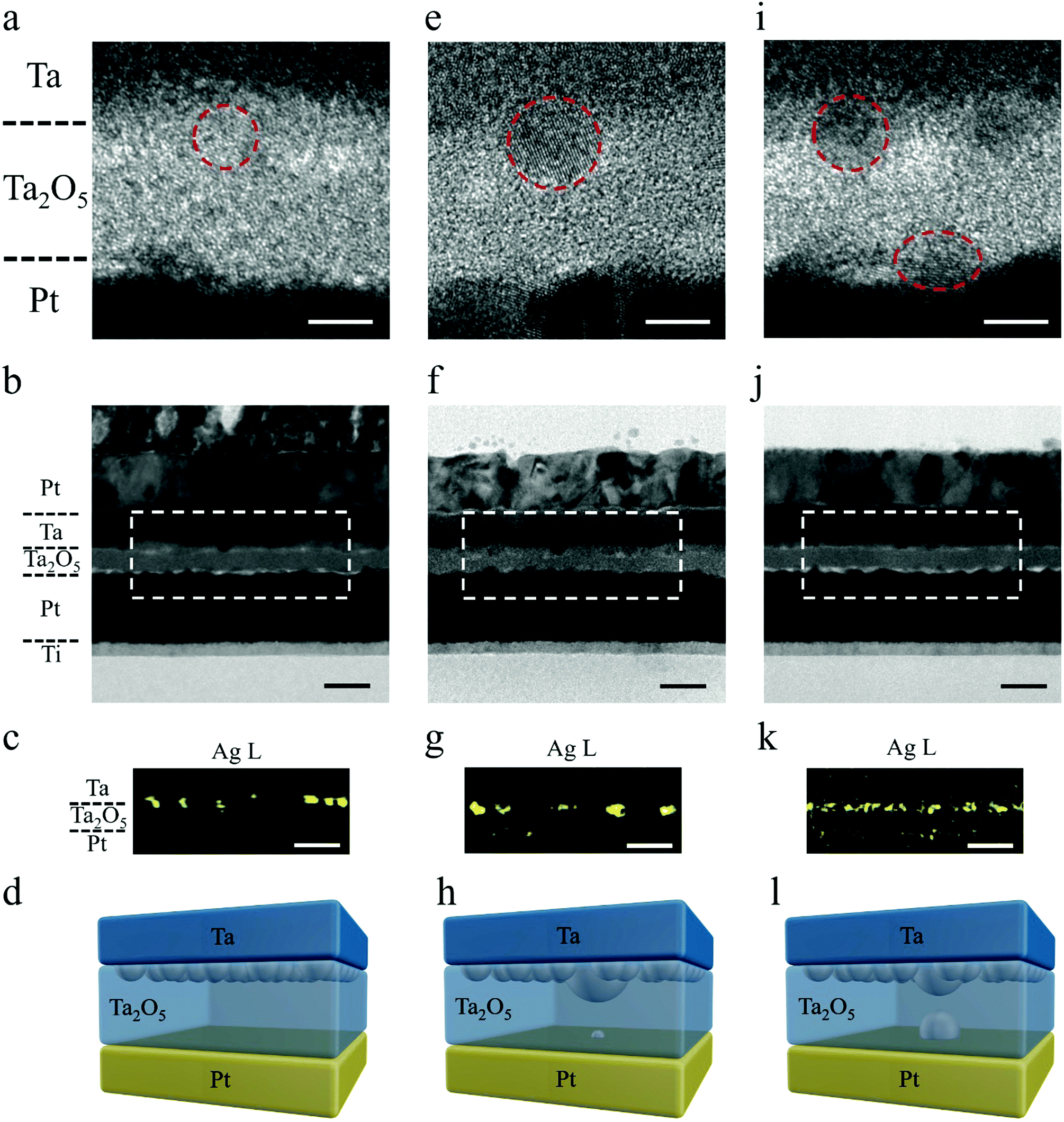 | ||
| Fig. 2 Field-directed migration and redistribution of Ag nanoclusters showing the mechanism of short-term and long-term plasticity. (a–d) High resolution TEM (a), low-resolution TEM (b), and the corresponding EDS mapping on Ag distribution (c) in pristine devices. Inclusion of Ag nanoclusters at the top interface can be observed and depicted in (d). (e–h) High resolution TEM (e), low-resolution TEM (f), and the corresponding EDS mapping on Ag distribution (g) in a device showing short-term plasticity. A low concentration of Ag at the bottom interface can be observed, implying that a weak Ag filament has been formed, but has spontaneously broken into discrete nanoclusters after removing the electrical signals in order to minimize the surface energy, causing short-term plasticity (h). (i–l) High resolution TEM (i), low-resolution TEM (j), and the corresponding EDS mapping on Ag distribution (k) in a device showing long-term plasticity. Existence of high Ag concentration at the bottom interface can be clearly identified and a certain Ag concentration was also detected in the dielectric, which has narrowed the effective thickness of the dielectric and resulted in long-term plasticity (l). Scale bars in high resolution TEM images, 5 nm. Scale bars in low resolution TEM images, 20 nm. | ||
The above dynamics of Ag nanoclusters in the present memristors bears striking similarity with synaptic Ca2+ dynamics, as depicted in Fig. 1b–e. In biological synapses, Ca2+ dynamics is responsible for both STP and LTP, forming the basis of memory and learning.34–36 While STP is linked with transient enhancement of synaptic transmission caused by the Ca2+ influx through N-methyl-D-aspartate receptors (NMDAR) as shown in Fig. 1c, the transition from STP to LTP through repeated or strong stimulations originates from the Ca2+ accumulation inside the postsynaptic membrane by changing the number and/or conductance of α-amino-3-hydroxy-5-methyl-4-isoxazole-propionic acid receptors (AMPAR) (Fig. 1e). Similarly, in the Ta/Ag-NCs/Ta2O5/Pt/Ti memristor mediated by the redistribution and evolution of Ag nanoclusters, a single pulse with low amplitude can only excite a small amount of Ag into the dielectric (Fig. 1b), which resembles the influx process of Ca2+ ions, and a weak conduction channel might be formed consequently. After the electrochemical migration of Ag during the applied pulse, the clearance of the bridging Ag nanoclusters from the dielectric driven by the thermodynamic minimization of the surface energy of Ag filament is analogous to the extrusion process of Ca2+via plasma membrane Ca2+-ATPase (PMCA), hence leading to STP (Fig. 1f–h and 2e–h). However, if a stronger stimulation is applied or subsequent pulses arrive before the nanoclusters diffuse away, more Ag will be driven into and get accumulated in the dielectric through electrochemical processes, leading to further growth of the conduction channel (Fig. 1d), akin to the persistent influx of Ca2+ ions. Once enough Ag has entered the dielectric and arrived at the bottom interface, the conduction channel can retain its high conductance even after thermodynamic relaxation (Fig. 1i and 2i–l), which bears similarity with the accumulation of Ca2+ inside the postsynaptic membrane and the long-term modification of synaptic strengths by changing the number and/or conductance of AMPAR (Fig. 1d and e), accounting for LTP. If the device starts from a potentiated state instead, a negative voltage pulse applied on the device can drive the Ag nanoclusters already accumulated in the dielectric and at the bottom interface toward the top electrode, thus causing synaptic depression. However, since the Ag concentration at the top interface is still much higher (Fig. 2k), the overall concentration gradient will result in backward diffusion of Ag after removing the negative pulse, leading to recovery of the synaptic weight and thus the short-term depression (Fig. 1j and k). If a stronger negative pulse or a train of negative pulses is applied instead, a permanent reduction of Ag concentration in the dielectric and at the bottom interface can be triggered, giving rise to the transition from STD to LTD (Fig. 1l). All the above synaptic behaviors can therefore be consistently explained in the same physical picture, based on the competing electrochemical and thermodynamic processes and the resultant evolution of Ag nanoclusters.
In addition to the pulse amplitude modulated plasticity shown in Fig. 1f–l, the time scale of synaptic plasticity can also be manipulated by the number or rate of the applied pulses, which can be readily expected from the above physical mechanism. Taking the potentiation process as an example, Fig. 3a–c exhibits a transition from STP to LTP as the pulse number increases from 1 to 20, while the pulse amplitude, width and period are fixed at 0.45 V, 100 ms and 200 ms, respectively. In addition, we also show that EPSC and STP to LTP transition can be implemented by pulses within higher amplitude of 0.7 V and shorter width of 10 μs, as illustrated in Fig. S8 (ESI†). Furthermore, when a successive pulse train containing 10 pulses (0.2 V, 20 ms) is applied, the plasticity then largely depends on the stimulation rate or pulse interval. One can see that the amplitude of the EPSC current increases when the pulse rate increases from 0.2 to 20 Hz (Fig. 3d–f), once again bearing similarity with the spiking rate dependent plasticity (SRDP) or dynamic filtering characteristics in biological systems.37,38 The present devices can also mimic the paired-pulse facilitation (PPF) behavior,39 another important short-term phenomenon for temporal information processing. One can see from Fig. 3g and h that a larger pulse interval leads to a smaller conductance enhancement, and the red line represents fitting results using the double exponential decay function. All these behaviors in Fig. 3a–h can be consistently interpreted by the competing effects between inward electrochemical migration of Ag during the pulses and outward thermodynamic diffusion during the pulse intervals.
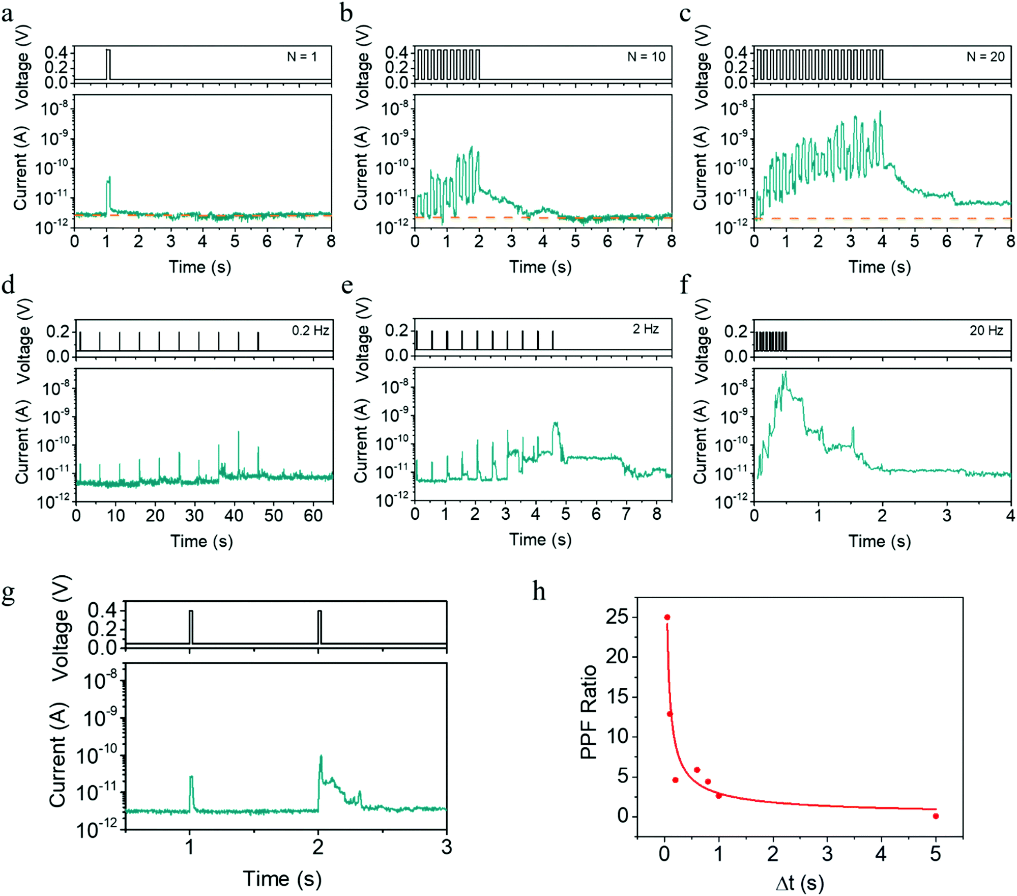 | ||
| Fig. 3 Synaptic plasticity with varied time scale manipulated by the number and rate of pulses, allowing the emulation of neuronal leaky integrate and fire dynamics. (a–c) Device response to identical voltage pulses (0.45 V, 100 ms) separated by a period of 200 ms with different pulse numbers (N = 1, 10, 20), showing a transition from STP to LTP that is analogous to biological systems. (d–f) Device response to a consecutive pulse train consisting of ten identical pulses (0.2 V, 20 ms) with different frequencies (0.2, 2, 20 Hz), which indicates spiking rate dependent plasticity or dynamic filtering characteristics. (g) PPF characteristics in the devices with a pair of pulses (0.4 V, 20 ms) applied with an interval of 1 s. (h) PPF ratio as a function of the pulse interval, where the red line represents fitting results using the double exponential decay function. | ||
Such electrochemical and thermodynamic processes of Ag naturally constitute an integration and leaking mechanism, which can be further used to emulate the leaky integrate and fire dynamics in biological neurons, as shown in Fig. 4a,3 provided that a reset signal is applied after neuronal firing to return the artificial neuron back to its resting state. We have tested the neuronal activity using different pulse intervals (Fig. 4) and found that the number of stimulations required to fire the neuron monotonously increases (7, 10, 17, 22) as pulse interval increases (0.1, 0.2, 0.5, 1 ms), thus demonstrating the leaky characteristic of the neuron during the pulse intervals. Consecutive cycles of neuron activity also showed that a rest period of 13.5 ms after neuronal firing can return the artificial neuron back to its resting state (Fig. S9, ESI†), even without a reset operation. Since the synaptic and neuronal functions are achieved in the same device structure, a compatibility in material systems and processes is ensured for the construction of hardware neural networks.
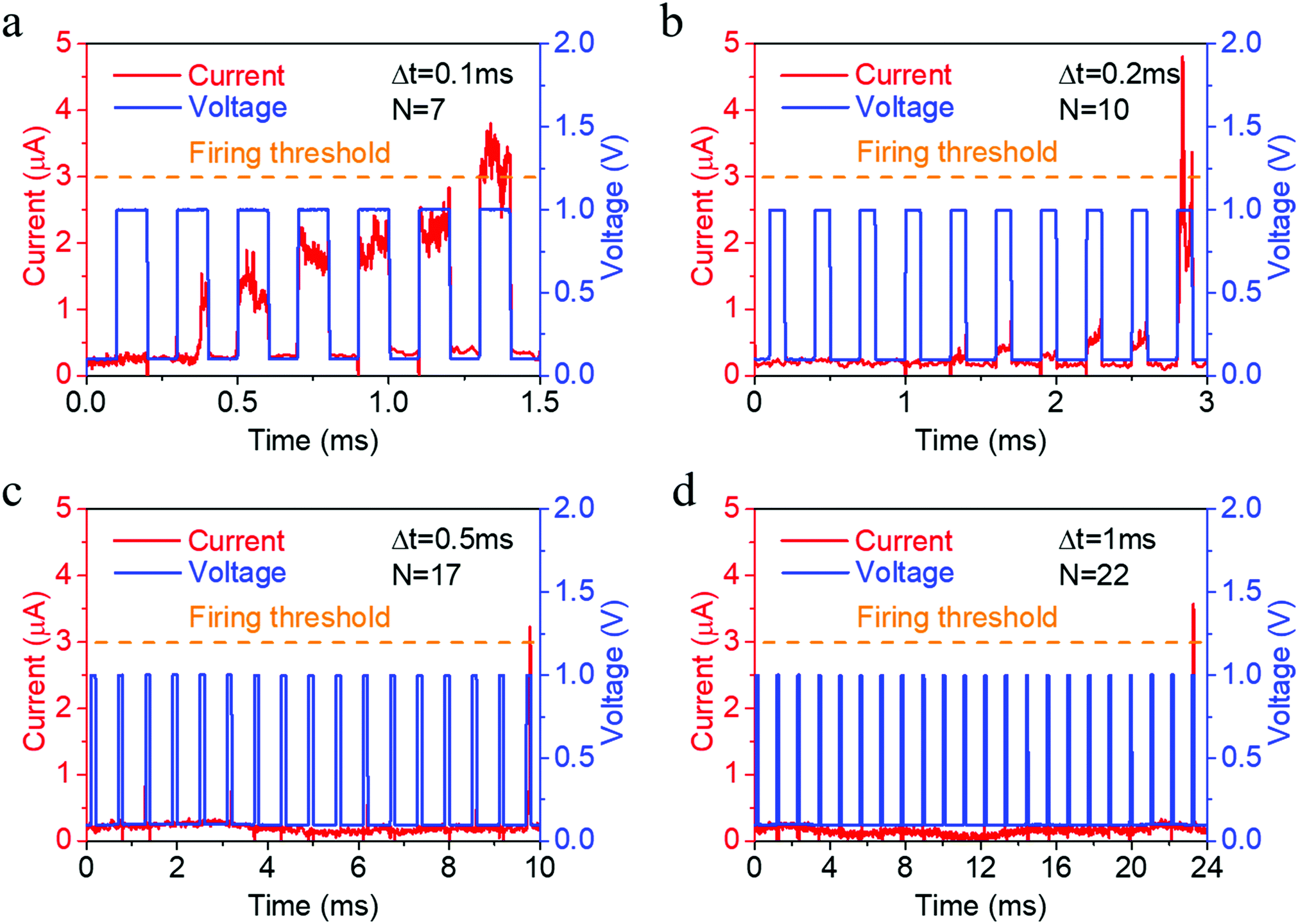 | ||
| Fig. 4 Emulation of neuronal activity using the Ta/Ag-NCs/Ta2O5/Pt/Ti devices with different pulse intervals (Δt), where the device current response (red) as a result of multiple voltage pulses (1 V, 100 μs, blue) physically emulates the leaky integrate and fire dynamics. (a–d) Emulation of neuronal activity using different numbers (7, 10, 17, 22) of voltage pulses (1 V, 100 μs, blue) with different pulse intervals (0.1, 0.2, 0.5, 1 ms). | ||
Notably, the first pulse in Fig. 4a did not result in visible change in the current, although the migration of Ag as a result of this pulse contributes to the subsequent apparent increase in device conductance. Herein, the first voltage pulse is equivalent with an internal modulator that regulates the following synaptic efficacy, which is reminiscent of metaplasticity in biological systems, a higher-order form of plasticity highlighting that the previous history of synaptic activities, even without affecting the efficacy of normal synaptic transmission, also plays a significant role in subsequent synaptic plasticity.40,41 The existence of metaplasticity in the Ta/Ag-NCs/Ta2O5/Pt/Ti synapses is further validated in Fig. 5a–d. One can see from Fig. 5a that the application of a programming pulse (0.5 V, 100 ms) triggers an EPSC with a magnitude of 50 μA, which then gradually decays over time and returns to the resting state in ∼0.3 s. When a weaker voltage pulse of (0.2 V, 100 ms) was applied, no obvious response in the device current can be detected after removing the pulse (Fig. 5b). However, the seemingly weak pulse can be adopted as an internal modulator of synaptic efficacy, where an enhanced EPSC has been successfully triggered by an identical programming pulse of (0.5 V, 100 ms) with Fig. 5a, if a preceding modulator pulse of (0.2 V, 100 ms) is applied (Fig. 5b–d). Moreover, the enhancement of the EPSC is a function of the interval between the modulator pulse and the programming pulse (Δt), where a decrease in Δt leads to higher amplitude and longer relaxation time in EPSC (Fig. 5b–d). A relatively long-term potentiation is observed when Δt decreases to 0.5 s, thus highlighting the role of the modulator pulse in manipulating the internal device state.
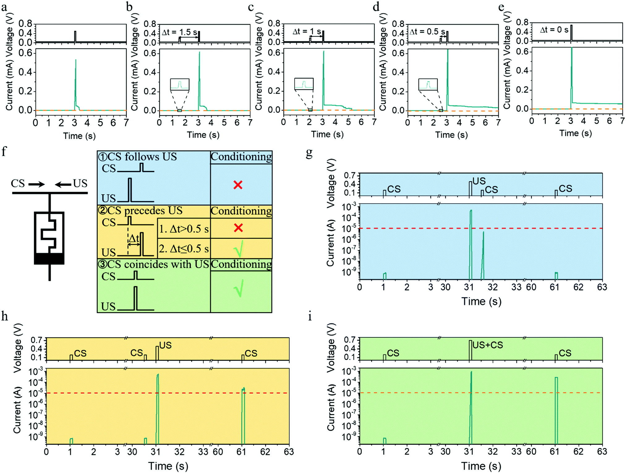 | ||
| Fig. 5 Implementation of metaplasticity and classical conditioning based on intrinsic device dynamics. (a–e) Implementation of metaplasticity in the device. (a) Device current response when a single programming pulse (0.5 V, 100 ms) was applied, where the current gradually decayed back to the resting state in about 0.3 s. (b–d) When a weak modulator pulse (0.2 V, 100 ms) was applied, an enhanced EPSC with higher amplitude and longer relaxation time can be triggered by the identical programming pulse as Δt decreases. A relatively long-term potentiation can be observed when the Δt decreases to 0.5 s. (f) Experimental setup and timing requirements of classical conditioning. Left panel: Experimental setup used for the implementation of classical conditioning. Right panel: Training outcomes after three different types of CS–US pairing. Conditioning occurs if the US and CS are presented simultaneously, or if the CS precedes the US by a short interval (≤0.5 s). Conditioning does not occur if the CS follows the US, or if the CS precedes the US by a large interval (>0.5 s). (g–i) Experimental results of training when different timing conditions of CS–US pairing were adopted, where CS and US pulses are (0.2 V, 100 ms) and (0.5 V, 100 ms), respectively, showing the successful implementation of classical conditioning. | ||
The metaplasticity demonstrated in Fig. 5a–d exhibits two important characteristics, internal state modulation and inherent timing mechanism, and they can be further utilized to implement important learning rules for spiking neural networks. Pavlov's dog is a famous example of classical conditioning or associative learning, which can be realized even on the synaptic level without sophisticated neural hardware, as discovered in Aplysia.42–46 In general, classical conditioning involves associating a stimulus that evokes a measurable response with a second stimulus that normally does not evoke this response. The first type of stimulus that normally evokes the response is called the unconditional stimulus (US), because no training (conditioning) is required for it to yield a response. The second type of stimulus that normally does not evoke the same response is called the conditional stimulus (CS), where training (conditioning) is required before it can yield the response. Although classical conditioning has been demonstrated previously using memristors by synchronously presenting CS and US during training,47,48 it is important to point out that classical conditioning in biology is asynchronous and has a more relaxed timing requirement, that is, conditioning will occur not only when the US and CS are presented simultaneously but also when the CS precedes the US by a short interval (≤0.5 s),45,49 as illustrated in Fig. 5f. Such asynchronous learning is certainly more robust. To emulate such asynchronous classical conditioning, the synaptic elements must have an internal modulator that times the interval between CS and US, which can be readily implemented using our Ta/Ag-NCs/Ta2O5/Pt/Ti devices, as shown in Fig. 5g–i. Herein, a pulse of (0.2 V, 100 ms) was used as the CS, which cannot evoke the response (defined as a current exceeding 10 μA) by itself, while a pulse of (0.5 V, 100 ms) was set as the US, which can yield the response by itself but without causing a long-term change. Therefore, when US precedes CS by 0.5 s, no long-term change in the device conductance is triggered after training, so CS itself still cannot evoke the response (Fig. 5g). In stark contrast, when CS was ahead of US by 0.5 s (Fig. 5h), the experimental condition is identical with that in Fig. 4d and a long-term potentiation can be obtained. As a result, the CS pulse was able to evoke the response after training (Fig. 5h). When the interval between CS and US was reduced to zero, namely the CS and US were presented synchronously, successful conditioning can also be achieved (Fig. 5i). Such associative learning demonstrated in Fig. 5g–i once again originates from the internal state modulation and timing mechanism as a result of Ag cluster dynamics, which will be important for building robust hardware networks. For instance, the classical conditioning could be used to learn and detect temporal correlations in event-based data streams based on unsupervised learning (see the illustration in Fig. S10 and related discussions, ESI†).
Last but not the least, the internal state modulation and inherent timing mechanism can also naturally lead to STDP, another important timing-based learning rule in biological systems,50 where the relative timing between the pre- and postsynaptic spikes determines whether the synaptic weight will be potentiated or depressed and by how much. In neurobiology, the relative timing information between the spikes is natively embedded, e.g. by the natural decay of Ca2+ levels providing an internal timing mechanism. To achieve STDP in hardware with similarly simple, non-overlapping pre- and postsynaptic pulse pairs, a natural timing mechanism in the synaptic element is demanded as well, which can be readily achieved by the diffusion dynamics of Ag. Fig. 6a–e shows the implementation of STDP in the present devices, where the pulse pair used contains a positive pulse of (0.3 V, 100 ms) representing the effect of a presynaptic spike and a negative pulse of (−0.45 V, 100 ms) representing the postsynaptic spike, applied both on the top electrode (Fig. 6d). Since the preceding positive (negative) pulse will cause short-term potentiation (depression) when Δt > 0 (Δt < 0), it is expected that the net effect of the pulse pair is determined by the residue effect of the preceding pulse, which increases as the absolute value of Δt decreases. Taking the case of Δt > 0 as an example, the residue effect of the preceding pulse becomes negligible when Δt is large enough (e.g. 1 s), resulting in little conductance change after the pulse pair (Fig. 6a). However, when Δt decreases, the residue effect of the preceding pulse counteracts with the contribution of the second pulse, resulting in a net synaptic potentiation (Fig. 6b and c). This eventually gives rise to the implementation of the STDP learning rule, as shown in Fig. 6e. It is worthwhile pointing out that the asymmetric pulse pair (0.3 and −0.45 V) could increase the complexity of peripheral circuitry during STDP learning. However, this might be addressed by further engineering the interfacial property especially the bottom Ta2O5/Pt interface and forming a higher Schottky barrier therein. As a result, the Ta2O5/Pt interface will cause larger voltage drop when it is reversely biased, which can in turn increase the amplitude of the positive pulses required and lead to a symmetric pulse pair during STDP. It should also be noted that when the pulse width and amplitude are reduced, the accompanying relaxation time is expected to decrease accordingly,8 which can therefore lead to reduced time gap Δt during the STDP and increase the training speed.
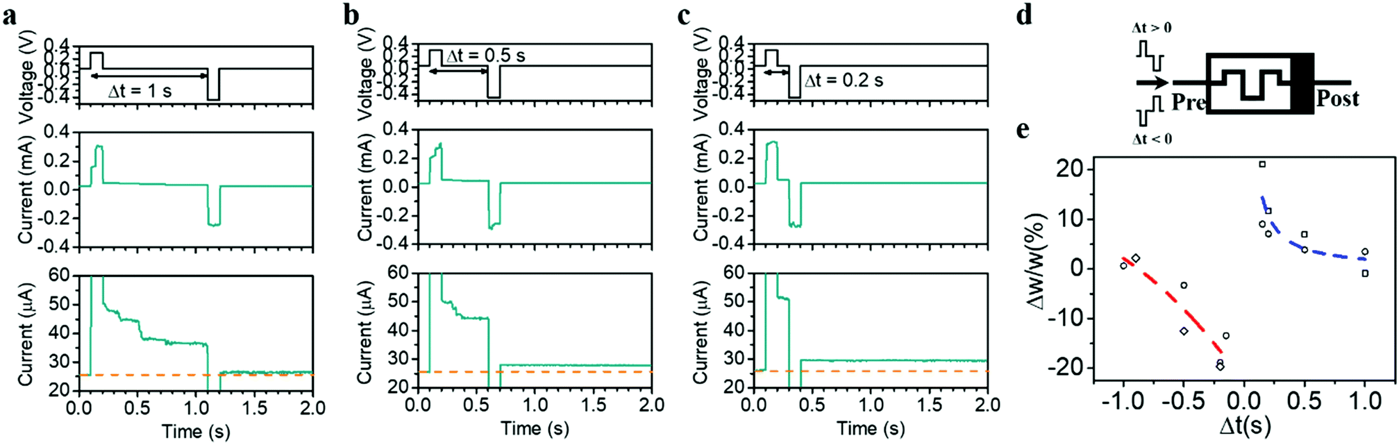 | ||
| Fig. 6 Biorealistic implementation of STDP based on intrinsic device dynamics. (a–c) Device current response to pre- and postsynaptic pulses with varied relative timing (0.2–1 s), where the pre- and postsynaptic pulses are (0.3 V, 100 ms) and (−0.45 V, 100 ms), respectively. (d) Schematic of the experimental setup for STDP implementation. (e) Weight change as a function of the relative timing between the pre- and postsynaptic pulses, showing the implementation of STDP in the artificial synapse. | ||
Conclusions
In summary, here we have shown that a two-terminal Ag-NCs based memristive synapse can be used to biorealistically realize STP and LTP not only in potentiation but also in the depression process, therefore holding potential for realizing complex cognitive functions in hardware by adjusting information transmission and network dynamics. The competing electrochemical and thermodynamic processes of Ag nanoclusters successfully emulate the calcium ion dynamics in biology and have been directly verified using detailed high resolution TEM and EDS analyses. Based on such intrinsic dynamics offering an internal state modulator and inherent timing mechanism, these memristive synapses have been employed to naturally implement more complex functions, including metaplasticity, asynchronous classical conditioning, and STDP. Aside from synaptic behaviors, the neuronal leaky integrate and fire dynamics can be physically captured using such devices as well. Note, that all the above functionalities were achieved based on the same robust physical mechanism exploiting the competing electrochemical and thermodynamic processes of Ag nanoclusters, without tailoring the programming conditions on purpose. Compared with existing studies, the present work shows simultaneous achievement of STP and LTP in both potentiation and depression processes, and the faithful emulation of calcium ion dynamics naturally leads to complex synaptic functions including metaplasticity, asynchronous classical conditioning and STDP using a simple two-terminal and scalable structure, and the synaptic and neuronal functions achieved in the same device structure ensure compatibility in material systems and processes, which represents the significance of this work. The demonstrated rich and asynchronous plasticity are crucial for robust learning with tunable information transmission and network dynamics, therefore making the present devices promising candidates for future construction of spiking based neuromorphic systems.Conflicts of interest
There are no conflicts to declare.Acknowledgements
This work was supported by the National Key R&D Program of China (Grant No. 2017YFA0207600), the National Natural Science Foundation of China (Grant No. 61674006 and 61421005), and the 111 Project (B18001).Notes and references
- P. A. Merolla, J. V. Arthur, R. Alvarez-Icaza, A. S. Cassidy, J. Sawada, F. Akopyan, B. L. Jackson, N. Imam, C. Guo, Y. Nakamura, B. Brezzo, I. Vo, S. K. Esser, R. Appuswamy, B. Taba, A. Amir, M. D. Flickner, W. P. Risk, R. Manohar and D. S. Modha, Science, 2014, 345, 668–673 CrossRef CAS.
- M. A. Zidan, J. P. Strachan and W. D. Lu, Nat. Electron., 2018, 1, 22–29 CrossRef.
- T. Tuma, A. Pantazi, M. Le Gallo, A. Sebastian and E. Eleftheriou, Nat. Nanotechnol., 2016, 11, 693–699 CrossRef CAS PubMed.
- M. Prezioso, F. Merrikh-Bayat, B. D. Hoskins, G. C. Adam, K. K. Likharev and D. B. Strukov, Nature, 2015, 521, 61–64 CrossRef CAS.
- G. W. Burr, R. M. Shelby, S. Sidler, C. d. Nolfo, J. Jang, I. Boybat, R. S. Shenoy, P. Narayanan, K. Virwani, E. U. Giacometti, B. N. Kurdi and H. Hwang, IEEE Trans. Electron Devices, 2015, 62, 3498–3507 Search PubMed.
- V. Ravichandran, C. Li, A. Banagozar, J. J. Yang and Q. F. Xia, Sci. China Inform. Sci., 2018, 61, 060423 CrossRef.
- S. Kim, C. Du, P. Sheridan, W. Ma, S. Choi and W. D. Lu, Nano Lett., 2015, 15, 2203–2211 CrossRef CAS PubMed.
- Z. Wang, S. Joshi, S. E. Savel'ev, H. Jiang, R. Midya, P. Lin, M. Hu, N. Ge, J. P. Strachan, Z. Li, Q. Wu, M. Barnell, G. L. Li, H. L. Xin, R. S. Williams, Q. Xia and J. J. Yang, Nat. Mater., 2017, 16, 101–108 CrossRef CAS PubMed.
- E. R. Kandel, J. H. Schwartz and T. M. Jessell, Principles of Neural Science, McGraw-Hill, New York, 4th edn, 2000 Search PubMed.
- G. Indiveri and S.-C. Liu, Proc. IEEE, 2015, 103, 1379–1397 CAS.
- D. B. Strukov, G. S. Snider, D. R. Stewart and R. S. Williams, Nature, 2008, 453, 80–83 CrossRef CAS.
- R. Waser, R. Dittmann, G. Staikov and K. Szot, Adv. Mater., 2009, 21, 2632–2663 CrossRef CAS.
- L. O. Chua, IEEE Trans. Circuit Theory, 1971, 18, 507–519 Search PubMed.
- Y. Yang and R. Huang, Nat. Electron., 2018, 1, 274–287 CrossRef.
- Y. Yang, B. Chen and W. D. Lu, Adv. Mater., 2015, 27, 7720–7727 CrossRef CAS.
- P. Yao, H. Wu, B. Gao, S. B. Eryilmaz, X. Huang, W. Zhang, Q. Zhang, N. Deng, L. Shi, H. S. P. Wong and H. Qian, Nat. Commun., 2017, 8, 15199 CrossRef CAS.
- L. Q. Zhu, C. J. Wan, L. Q. Guo, Y. Shi and Q. Wan, Nat. Commun., 2014, 5, 3158 CrossRef.
- S. H. Jo, T. Chang, I. Ebong, B. B. Bhadviya, P. Mazumder and W. Lu, Nano Lett., 2010, 10, 1297–1301 CrossRef CAS PubMed.
- T. Chang, S.-H. Jo and W. Lu, ACS Nano, 2011, 5, 7669–7676 CrossRef CAS PubMed.
- Z. H. Tan, R. Yang, K. Terabe, X. B. Yin, X. D. Zhang and X. Guo, Adv. Mater., 2016, 28, 377–384 CrossRef CAS.
- T. Ohno, T. Hasegawa, T. Tsuruoka, K. Terabe, J. K. Gimzewski and M. Aono, Nat. Mater., 2011, 10, 591–595 CrossRef CAS PubMed.
- Z. Q. Wang, H. Y. Xu, X. H. Li, H. Yu, Y. C. Liu and X. J. Zhu, Adv. Funct. Mater., 2012, 22, 2759–2765 CrossRef CAS.
- J. Zhu, Y. Yang, R. Jia, Z. Liang, W. Zhu, Z. U. Rehman, L. Bao, X. Zhang, Y. Cai, L. Song and R. Huang, Adv. Mater., 2018, 30, 1800195 CrossRef.
- E. J. Fuller, F. E. Gabaly, F. Léonard, S. Agarwal, S. J. Plimpton, R. B. Jacobs-Gedrim, C. D. James, M. J. Marinella and A. A. Talin, Adv. Mater., 2017, 29, 1604310 CrossRef.
- C. S. Yang, D. S. Shang, N. Liu, G. Shi, X. Shen, R. C. Yu, Y. Q. Li and Y. Sun, Adv. Mater., 2017, 29, 1700906 CrossRef.
- A. Baddeley, Science, 1992, 255, 556–559 CrossRef CAS.
- A. Baddeley, Nat. Rev. Neurosci., 2003, 4, 829 CrossRef CAS PubMed.
- S. Wu, K. Y. M. Wong and M. Tsodyks, Front. Comput. Neurosci., 2013, 7, 188 Search PubMed.
- A. Wedig, M. Luebben, D.-Y. Cho, M. Moors, K. Skaja, V. Rana, T. Hasegawa, K. K. Adepalli, B. Yildiz, R. Waser and I. Valov, Nat. Nanotechnol., 2016, 11, 67–74 CrossRef CAS PubMed.
- J. H. Yoon, J. Zhang, X. Ren, Z. Wang, H. Wu, Z. Li, M. Barnell, Q. Wu, L. J. Lauhon, Q. Xia and J. J. Yang, Adv. Funct. Mater., 2017, 27, 1702010 CrossRef.
- I. Valov, M. Luebben, A. Wedig and R. Waser, ECS Trans., 2016, 75, 27–39 CrossRef CAS.
- Y. Yang, P. Gao, L. Li, X. Pan, S. Tappertzhofen, S. Choi, R. Waser, I. Valov and W. D. Lu, Nat. Commun., 2014, 5, 4232 CrossRef CAS PubMed.
- H. Ling, M. Yi, M. Nagai, L. Xie, L. Wang, B. Hu and W. Huang, Adv. Mater., 2017, 29, 1701333 CrossRef.
- R. S. Zucker and W. G. Regehr, Annu. Rev. Physiol., 2002, 64, 355–405 CrossRef CAS.
- R. C. Malenka and M. F. Bear, Neuron, 2004, 44, 5–21 CrossRef CAS PubMed.
- D. E. Clapham, Cell, 2007, 131, 1047–1058 CrossRef CAS.
- K. L. Magleby, J. Physiol., 1973, 234, 327–352 CrossRef CAS.
- J. X. Bao, E. R. Kandel and R. D. Hawkins, Science, 1997, 275, 969–973 CrossRef CAS PubMed.
- P. A. Salin, M. Scanziani, R. C. Malenka and R. A. Nicoll, Proc. Natl. Acad. Sci. U. S. A., 1996, 93, 13304–13309 CrossRef CAS.
- W. C. Abraham and M. F. Bear, Trends Neurosci., 1996, 19, 126–130 CrossRef CAS PubMed.
- W. C. Abraham, Nat. Rev. Neurosci., 2008, 9, 387–399 CrossRef CAS PubMed.
- E. T. Walters, T. J. Carew and E. R. Kandel, Proc. Natl. Acad. Sci. U. S. A., 1979, 76, 6675–6679 CrossRef CAS PubMed.
- T. J. Carew, E. T. Walters and E. R. Kandel, J. Neurosci., 1981, 1, 1426–1437 CrossRef CAS PubMed.
- G. G. Murphy and D. L. Glanzman, Science, 1997, 278, 467–471 CrossRef CAS PubMed.
- R. Hawkins, T. Carew and E. Kandel, J. Neurosci., 1986, 6, 1695–1701 CrossRef CAS.
- T. Carew, R. Hawkins and E. Kandel, Science, 1983, 219, 397–400 CrossRef CAS.
- M. Ziegler, R. Soni, T. Patelczyk, M. Ignatov, T. Bartsch, P. Meuffels and H. Kohlstedt, Adv. Funct. Mater., 2012, 22, 2744–2749 CrossRef CAS.
- Y. V. Pershin and M. Di Ventra, Neural Networks, 2010, 23, 881–886 CrossRef.
- M. F. Bear, B. W. Connors and M. A. Paradiso, Neuroscience: Exploring the Brain, 3rd edn, Lippincott Williams & Wilkins, USA, 2007 Search PubMed.
- N. Caporale and Y. Dan, Annu. Rev. Neurosci., 2008, 31, 25–46 CrossRef CAS.
Footnote |
| † Electronic supplementary information (ESI) available: Fig. S1–S10. See DOI: 10.1039/c9mh01206k |
| This journal is © The Royal Society of Chemistry 2020 |