
 Open Access Article
 This Open Access Article is licensed under a Creative Commons Attribution-Non Commercial 3.0 Unported Licence
Tuning cesium–guanidinium in formamidinium tin triiodide perovskites with an ethylenediammonium additive for efficient and stable lead-free perovskite solar cells†
Gabriella A.
Tosado
,
Erjin
Zheng
 and
Qiuming
Yu
*
and
Qiuming
Yu
*
Department of Chemical Engineering, University of Washington, Seattle, WA 98195, USA. E-mail: qyu@u.washington.edu
First published on 25th November 2020
Abstract
Achieving efficient and stable tin-based perovskite solar cells remains challenging. In this work, we incorporate the ethylenediammonium diiodide (EDAI2) additive into a cesium–guanidinium doped formamidinium tin triiodide perovskite with the composition of (CsGA)xFA1−2xSnI3 + y% EDAI2. This new perovskite utilizes the strong hydrogen bonding of the guanidinium cation and the lattice strain relaxation of the small cesium cation as well as the hollowing and passivation effects of the EDAI2 additive. The EDAI2 additive not only yields pinhole-free cubic phase perovskite films but also decreases both shallow and deep trap states in the perovskite films. These effects are pronounced with the increase of substitution of the pair of GA+ and Cs+. The new perovskites are deployed in inverted planar solar cells. A maximum power conversion efficiency (PCE) of 5.01% is achieved with the (CsGA)0.15FA0.70SnI3 + 0% EDAI2 device but the device degrades after storage in a nitrogen-filled glove box for 30 days. Both performance and stability are improved with the addition of EDAI2. A maximum PCE of 5.72% is achieved with the (CsGA)0.15FA0.70SnI3 + 1.0% EDAI2 device. The (CsGA)0.15FA0.70SnI3 + 1.5% EDAI2 devices exhibit a maximum PCE of 5.69% and the performance is further increased to 6.39% after storage in a nitrogen-filled glove box for 4 days; 70% of the initial PCE is retained after 45 days. This study demonstrates the benefit of tuning cation sizes and introducing divalent cations to integrate stabilizing factors into pure Sn perovskites, creating new routes for efficient and stable lead-free perovskite solar cells.
Introduction
Perovskite solar cells (PVSCs) have progressed rapidly in recent years. With the record power conversion efficiency (PCE) reaching 25.2%1 and the potential for cost effective roll-to-roll printing capabilities, PVSCs are well positioned to encourage a transition to a clean energy economy. However, the toxicity of lead-based perovskite materials and the low stability and poor performance of lead-free perovskite alternatives present a challenge towards commercialization of perovskite technologies. Tin-based perovskites have been investigated as low-toxic alternatives to lead-based perovskites because tin has a comparable ionic radius (Sn2+, 1.15 Å and Pb2+, 1.19 Å)2 and is also a group 14 metal, allowing Sn to maintain the crucial MX6 octahedron.3 Tin-based perovskites have certain intrinsic advantages over lead-based perovskites for photovoltaic devices such as a more favorable, comparably smaller bandgap, resulting in a higher Shockley–Queisser limit, and a more rapid charge carrier mobility.4,5 Unfortunately, the main drawback of pure Sn perovskites is an oxidation reaction that hinders photovoltaic performance. Tin-containing PVSCs have been shown to degrade from the oxidation of Sn2+ to the more thermodynamically favored Sn4+, even in inert atmospheres, due to the small activation energy for the oxidation reaction.6,7 The high levels of self-p-doping caused by Sn4+ create a high defect density, also resulting in a low open-circuit voltage, Voc.8One strategy for improving the performance and stability of tin-based PVSCs has been focusing on A-site cation mixtures. Single A-site cation pure Sn perovskites, such as cesium tin triiodide (CsSnI3), methylammonium tin triiodide (MASnI3), and formamidinium tin triiodide (FASnI3), have been thoroughly explored in previous studies.9 Although CsSnI3 was the first explored active layer for pure Sn PVSCs, it has been plagued with a low PCE and Voc because of its small tolerance factor, creating an orthorhombic perovskite phase.10,11 MASnI3 PVSCs demonstrated promising performance with a PCE of 6%. However, the devices were unstable and had poor reproducibility because of poor film morphology and Sn oxidation.12,13 FASnI3 was hypothesized to be more stable against oxidation because of increased hydrogen bonding and a lower dipole moment, allowing it to better rotate in the octahedral cage and interact with the halides.9,14
Recently, another organic cation has been demonstrated to further protect Sn against oxidation.15 Guanidinium (GA+) cations have been used in Sn based PVSCs to improve performance and stability under ambient conditions. Due to the larger ionic radius of GA+ (r = 2.78 Å) compared with FA+ (r = 2.53 Å) and MA+ (r = 1.80 Å), density functional theory (DFT) calculations predict that cubic-phase GASnI3 will have a shorter hydrogen bonding length and stronger interactions with the SnI6 octahedron.16 The higher amounts of bonded amines create a symmetrical structure in GA+ and a zero electric dipole moment, unlike FA+ and MA+, allowing for freer rotation of GA+ in the SnI6 framework. The high hydrogen bonding capability and free rotation enable GA+ to effectively passivate under-coordinated iodide ions, resulting in longer carrier lifetimes and an increased Voc because of the reduced recombination centers.17 The capability of passivating under-coordinated iodide ions is particularly important for pure Sn perovskites because iodide vacancies induce the oxidation of Sn2+ to Sn4+.7 In addition, the incorporation of GA+ into FASnI3 reduces the tendency of phase segregation because of the multiple hydrogen bonding sites. Therefore, GA+ is an excellent candidate for stabilizing mixed A-site Sn based perovskites. However, simply incorporating GA+ into GA0.20FA0.80SnI3 perovskites yielded very low efficiency PVSCs with a PCE of 0.5% even though extra SnF2 was added as a reducing agent.15 This could be due to the increased local lattice strain created by introducing such a large organic cation. The increased local lattice strain has been theorized to be due to increasing point defect formation to relieve the strain.18 The increased point defects could be the sites for oxidation and/or trap centers, affecting the performance of Sn-based PVSCs significantly.
One method that has been shown to “hollow” out three-dimensional (3D) perovskites and reduce lattice strain is introducing ethylenediammonium diiodide (EDAI2). EDAI2 has been explored as an A-site cation in 3D FASnI3 and MASnI3 perovskites.19 Shallow trap states are localized in the crystal bulk structure and are located near the conduction or valence band edges. Deep trap states involve grain boundary defects and are located closer to the middle of the band gap.20,21 The incorporation of such a large divalent cation results in not only the occupation of A-sites, but also the removal of B- and X-sites, reducing both bulk defects and shallow trap states. In addition, the divalent cations terminate crystal surfaces, reducing deep trap states at grain boundaries. The performance of FASnI3 PVSCs improved from a PCE of 1.40% without EDAI2 to 7.14% with 10% EDAI2 and the efficiency was maintained after 1000 h for encapsulated devices.19 It has been demonstrated that incorporating EDAI2 into MASnI3 lowers the electron trap state density and increases the carrier lifetime, which leads to an improvement of the device performance from a PCE of 0.17% without EDAI2 to 5.49% with 15% EDAI2.22 The significant improvement of device performance and stability is attributed to the occupation of point defects inside the crystalline grains and the passivation of defects at grain boundaries by EDAI2 cations, decreasing both shallow and deep trap states. Adding EDAI2 to FA0.80GA0.20SnI3 greatly enhanced the device performance from a PCE of 0.5% without EDAI2 to the maximum PCE of 7.4% with 1% EDAI2.23 More interestingly, the PCE even increased to a maximum of 8.9% after the device was stored in a glove box for over 1400 h. The fascinating behavior is due to the slow crystal relaxation and surface passivation induced by EDAI2. Another method of reducing lattice strain caused by a large organic cation is the addition of a smaller counter ion, such as Cs+. A small cation can fill point defects, reducing shallow trap states and protecting the sites from oxidation.18 Using Cs+ to counterbalance the large GA+ cation in a FASnI3 perovskite should allow the retention of the stabilizing effects of GA+ while reducing the local lattice strain, thus improving the performance of the corresponding devices.
In this study, we implement both GA+ and Cs+ cations into the FASnI3 crystal structure to introduce more hydrogen bonding and to reduce local strains, respectively, within the perovskite crystals (Fig. 1a–d). We further incorporate EDAI2 to replace some octahedral sites inside the crystal and to passivate defects at the grain boundaries (Fig. 1d) to relax lattice strains and reduce oxidation and trap states. We successfully synthesize densely packed, lead-free polycrystalline (CsGA)xFA1−2xSnI3 films with EDAI2. To reduce transport layer impacts on Sn oxidation, we use the inverted device structure of indium tin oxide (ITO)/poly(3,4-ethylenedioxythiophene):polystyrene sulfonate (PEDOT:PSS)/perovskite/[6,6]-phenyl-C60-butyric acid methyl ester (PC60BM)/2,9-dimethyl-7,7-diphenyl-1,10-phenanthroline (BCP)/Ag. The substitution of FA+ with the pair of Cs+ and GA+ leads to a (CsGA)0.15FA0.70SnI3 device with a maximum PCE of 5.01%, much higher than that obtained simply by the incorporation of GA+ in GA0.20FA0.80SnI3, but the device loses the diode behaviour after storage in a nitrogen-filled glove box for 30 days. With the EDAI2 additive, freshly made (CsGA)0.15FA0.70SnI3 with 1% EDAI2 devices exhibit a record maximum PCE of 5.72%. The UV-Vis absorption and ultraviolet photoelectron spectroscopy (UPS) results show that the addition of EDAI2 reduces the amount of trap states in perovskite thin films, improving the short-circuit current, Jsc, and the open-circuit voltage, Voc. Devices made with (CsGA)0.15FA0.70SnI3 and 1.5% EDAI2 exhibit a maximum PCE of 5.69% and the maximum PCE increases to 6.39% after storage in a nitrogen-filled glove box for 4 days; the device retains 70% of the initial PCE after 45 days. Thin film trap state reduction and device stability improvement highlight the importance of EDAI2 as a mitigating agent. Tuning cation sizes and integrating divalent cations create new routes for developing efficient and stable pure Sn PVSCs.
 | ||
| Fig. 1 SnI6 inorganic framework highlighting N–H–I hydrogen bonding in (a) MASnI3, (b) FASnI3, and (c) GASnI3. (d) Schematic illustration of the 3D (CsGA)xFA1−2xSnI3 perovskite with the EDAI2 additive showing EDA2+ cations creating potential hollowing inside the crystal as well as passivating defects along the grain boundaries. Yellow, purple, red, grey, blue, and green spheres represent Sn, Cs, I, H, C, and N atoms, respectively, and octahedra are marked by blue squares. | ||
Experimental
Materials
Tin(II) iodide (SnI2, 99.99%), cesium iodide (CsI, 99.999%), chloroform (≥99.99%), chlorobenzene (anhydrous, 99.8%), N,N-dimethyl sulfoxide (DMSO, anhydrous, ≥99.9%), 2-propanol and bathocuproine (BCP, 99.99%) were purchased from Sigma-Aldrich (St. Louis, Missouri) without further purification. Guanidinium iodide (GAI) and formamidinium iodide (FAI) were purchased from GreatCell Solar (Queanbeyan, Australia) while ethylenediammonium diiodide (EDAI2) was purchased from Millipore and used without further purification. [6,6]-Phenyl-C61-butyric acid methyl ester (PC60BM) (>99.5%) was purchased from American Dye Solar (Quebec, Canada).Thin film fabrication
The perovskite precursor solutions were prepared in a N2 glove box by dissolving FAI and SnI2 at the corresponding molar ratios in pure DMSO with a total concentration of 2.0 M. 10 mol% excess SnI2 was added into the precursor solution to reduce vacancies. CsI, GAI, and EDAI2 were dissolved in separate vials of DMSO at a concentration of 1.5 M and added to the perovskite precursor to achieve the correct triple cation composition. For the (CsGA)0.15FA0.70SnI3 composition with 1% EDAI2, for example, 0.1204 g of FAI and 0.4098 g of SnI2 were dissolved in 850 μl of DMSO and stirred at 60 °C for 0.5 h. 100 μl of the 1.5 M CsI solution and 100 μl of the 1.5 M GAI solution were added to the precursor and stirred continuously at 60 °C for 0.5 h. 14 μl of the 1.5 M EDAI2 solution was finally added to the precursor solution and stirred overnight at room temperature. The final precursor solution was then filtered through a 0.2 μm PTFE filter before use. Plain glass was cut into 15 mm × 15 mm substrates, which were cleaned via ultrasonication for 15 min in detergent in Millipore deionized water, Millipore deionized water, acetone, and isopropanol in sequence. The substrates were treated with oxygen plasma at 100 W for 10 min. A 70 μl drop of the precursor solution was spin-coated on a cleaned glass substrate at 500 rpm for 5 s, 1000 rpm for 15 s, and 4000 rpm for 40 s in a nitrogen glove box. 500 μl of chlorobenzene anti-solvent was dripped in situ onto the substrate during the last 15 s of the third spin-coating step. The perovskite films were then thermally annealed at 110 °C for 10 min.Film characterization
Scanning electron microscopy (SEM) images were acquired using an FEI Sirion SEM operated at 15 kV to analyze the surface morphology. Two-dimensional X-ray diffraction (XRD) patterns were collected with a Bruker GADDS D8 Focus Powder Discover diffractometer using Cu Kα radiation (λ = 1.5419 Å) and the data were processed using the EVA package provided by Bruker AXS to investigate the crystalline structures of perovskite thin films. Ultraviolet-visible (UV-Vis) absorption spectra were collected using a Varian Cary 5000 UV-Vis-NIR spectrophotometer. Photoluminescence (PL) spectra were obtained with a Horiba HR-800 with 532 nm laser excitation. Ultraviolet photoelectron spectroscopy (UPS) measurements were conducted using a Kratos AXIS Ultra DLD spectrometer to investigate the valence band structures of perovskite thin films. A He discharge lamp source (Kratos) at an excitation energy of 21.2 eV was used in combination with a delay line detector at an electron pass energy of 5 eV. The UPS spectra for Au were acquired with a step size of 0.1 eV and a dwell time of 100 ms. The high-resolution UPS spectra and Fermi edge spectra were acquired with a step size of 0.01 eV and a dwell time of 100 ms.Device fabrication
ITO coated glass substrates (10 Ohm sq−1 ITO, Colorado Concept Coatings LLC) were cut and cleaned as described above. The PEDOT:PSS (AI 4083, Heraeus CleviosTM) solution was filtered with a 0.45 μm nylon filter. A 70 μl drop of PEDOT:PSS was spin-coated on a cleaned ITO coated glass substrate at 5000 rpm for 60 s and annealed at 150 °C for 10 min in air. The substrates were transferred to a N2 glove box and the perovskite thin films were fabricated as described above. A PC60BM solution (15 mg ml−1 in chloroform) was then spin-coated on the perovskite films at 4000 rpm for 60 s and dried without annealing. A BCP solution (0.5 mg ml−1 in 2-propanol) was then spin-coated on the films at 4000 rpm for 60 s and dried without annealing. Finally, a mask with 3.14 × 10⁻⁶ m2 area holes was placed on substrates that were loaded into a thermal evaporation chamber to thermally deposit 100 nm of silver as electrodes in a high vacuum evaporator (<1 × 10⁻⁶ Torr). The resulting device structure is ITO/PEDOT:PSS/perovskite/PC60BM/BCP/Ag.Device performance tests
The photocurrent density–voltage (J–V) curves, light intensity dependent J–V curves, and steady-state photocurrent measurements were conducted in a N2 glove box with a Keithley 2400 SourceMeter and a Solar Light Co. Xenon lamp (16S–300 W) and AM 1.5G filter. Before measurements, the light intensity was calibrated to 100 mW cm−2 using a standardized National Renewable Energy Laboratory calibrated silicon solar cell.Results and discussion
A one-step solution process with the chlorobenzene anti-solvent was used to form the pure Sn perovskite films. All precursors (FAI, SnI2, GAI, CsI, and EDAI2) were dissolved in pure DMSO to a total concentration of 2.0 M and spin-coated on ITO/glass substrates. 10 mol% excess SnI2 was added to suppress the vacancies in the crystal lattice. All films were annealed at 110 °C for 10 min. The pure Sn perovskite films have the compositions of (CsGA)xFA1−2xSnI3 + y% EDAI2, where x = 0.05, 0.10, 0.15, and 0.20 and y = 0, 0.5, 1.0, 1.5, and 2.0. To simplify further discussion, we implement a notation of (CsGA)x, where x is the percentage of cation added, to represent the various compositions. For example, (CsGA)5 would represent (CsGA)0.05FA0.90SnI3. The anti-solvent wash with the highly non-polar chlorobenzene was performed while spin-coating to remove excess DMSO from SnI2·3DMSO. The removal of excess DMSO results in the formation of A-SnI2–2DMSO intermediates, allowing the slower removal of DMSO and growth of polycrystalline perovskite thin films upon annealing, thus minimizing pinholes. Although SnF2 has been used to minimize the oxidation of Sn2+ to Sn4+, excess SnF2 has been shown to form separate phases and phase segregation on perovskite film surfaces or grain boundaries over time.14,24 Excess SnI2 has been shown to be effective in preventing Sn2+ oxidation by both compensating and suppressing Sn2+ vacancies without having any adverse side effects on phase stability and phase segregation.25,26 Previous research has argued that excess SnI2 may even be more effective than SnF2 as a reducing agent since SnF2 is hard to dissociate in films because of its low solubility and stability.27 To minimize SnF2 assisted phase segregation, we use excess SnI2 plus EDAI2 to reduce Sn2+ oxidation.Fig. 2a shows the scanning electron microscopy (SEM) images of the synthesized (CsGA)15 + y% EDAI2 perovskite thin films. Without the addition of EDAI2, (CsGA)15 films contain flat, large grains and pinholes, which may be due to the presence of a few nuclei and a rapid crystal growth rate.28 EDAI2 has been previously shown to act as a controlling agent and balance the kinetic processes between crystal growth and nucleation. The divalent nature of EDAI2 allows uniform nucleation and, in tandem with the slow crystal growth, forming densely packed perovskite films.23 Because of this increased nucleation, from 0 to 1.0% EDAI2, there is a decrease in grain size and the number of pinholes. Dense, small grains are formed for the (CsGA)15 + 1.0% EDAI2 film. Fig. S1a (ESI†) shows the corresponding SEM images for (CsGA)5 + y% EDAI2 and (CsGA)10 + y% EDAI2 perovskite thin films, which illustrate a similar trend of decreasing grain size and pinholes from 0 to 1.0% EDAI2. When increasing EDAI2 to 1.5% and 2%, the perovskite grains jut out from the surfaces, as shown in Fig. 2a for (CsGA)15 and in Fig. S1a (ESI†) for the (CsGA)5 and (CsGA)10 films. This effect has been observed more drastically with 5% EDAI2 incorporation, coupled with a decreased crystal density due to the replacement of B- and X-sites.29 Fig. S2 (ESI†) shows the low magnification SEM images of all (CsGA)x + y% EDAI2 films to demonstrate the consistency of film morphologies.
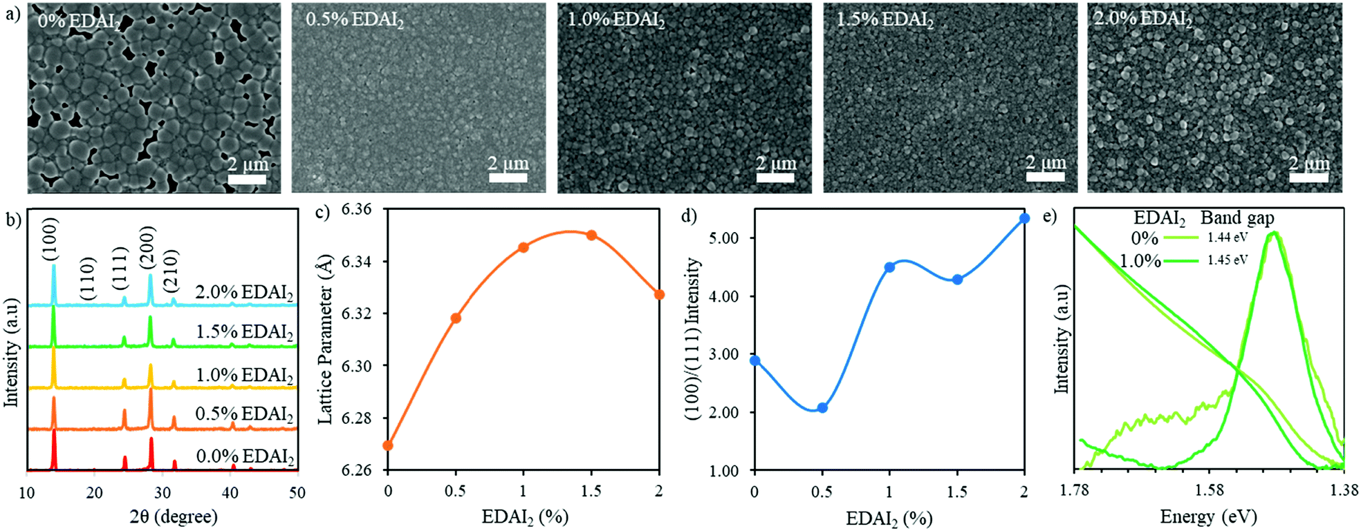 | ||
| Fig. 2 (a) SEM images and (b) XRD patterns of (CsGA)15 + y% EDAI2 perovskite thin films with y = 0, 0.5, 1.0, 1.5, and 2.0. (c) The cubic lattice parameter and (d) the (100)/(111) peak intensity ratio of (CsGA)15 + y% EDAI2 as a function of percent EDAI2. (e) PL spectra and normalized UV-Vis absorption spectra of (CsGA)15 thin films with 0 and 1.0% EDAI2. The optical band gaps are derived from the Tauc plots of (CsGA)15 thin films with 0 and 1.0% EDAI2 in Fig. S6e (ESI†). | ||
X-ray diffraction (XRD) was used to characterize the phase and crystallinity of the thin films. Fig. 2b shows the XRD patterns of (CsGA)15 + 0–2.0% EDAI2 thin films and the XRD patterns of (CsGA)5 and (CsGA)10 with the same range of EDAI2 are shown in Fig. S1b (ESI†). A previous study reported a pseudo cubic orthorhombic phase for FASnI3 with the Amm2 space group.19 We compare the XRD pattern of the (CsGA)15 + 1.0% EDAI2 film and the simulated XRD patterns of FASnI3 with the cubic Pm3m and orthorhombic Amm2 space groups in Fig. S3 (ESI†). The XRD pattern of the (CsGA)15 + 1.0% EDAI2 film matches very well with the peaks corresponding to the cubic phase and does not show any peak splitting or characteristic peaks of the orthorhombic phase. Kubicki et al. used NMR to obtain direct evidence of GA+ incorporation into the MAPbI3 and FAPbI3 lattice forming phase-pure materials, dispelling the hypothesis that GA+ is too large to enter the perovskite crystal structure.30 We estimated the average A-site cation radii with mixed triple cations and calculated the Goldschmidt tolerance factors of (CsGA)xFA1−2xSnI3 without EDAI2 based on the average A-site cation radii (Table S1, ESI†). As the concentration of FA+ (r = 2.53 Å) decreases and the concentrations of both Cs+ (r = 1.67 Å) and GA+ (r = 2.78 Å) increase, the average A-site cation radius decreases from 2.50 Å (CsGA)5 to 2.47 Å (CsGA)10 to 2.44 Å (CsGA)15 (Table S1, ESI†). This trend is reflected in a decrease in the lattice parameter from 6.291 Å to 6.274 Å to 6.269 Å for (CsGA)5, (CsGA)10, and (CsGA)15, respectively, with 0% EDAI2 (Fig. 2c and Fig. S1c, ESI†), indicating the incorporation of CsGA into the perovskite crystal structures. The incorporation of CsGA suppresses the tolerance factor of FASnI3, pushing the tolerance factor into the more ideal cubic region (Table S1, ESI†). Without EDAI2, (CsGA)5 and (CsGA)10 have the tolerance factors of 0.992 and 0.986, respectively, approaching the tetragonal/hexagonal region. Small peaks emerging at 13.28° and 12.12° in the XRD patterns of (CsGA)5 and (CsGA)10 with 0% EDAI2 thin films, respectively shown in Fig. S1b (ESI†), might be attributed to the orthorhombic impurity phase due to higher tolerance factors. No impurity phase peaks are present in the XRD pattern of the (CsGA)15 thin film with 0% EDAI2 because the tolerance factor has been pushed far enough into the ideal cubic region (Table S1, ESI†). Although further increasing the CsGA content can reduce the average A-site radii and tolerance factors, both XRD patterns and SEM images show the formation of 2D guanidinium based perovskites and diminished 3D perovskites in (CsGA)20 + 0–1.0% EDAI2 thin films (Fig. S4, ESI†). With 0% EDAI2, there are large sheets in the SEM images (Fig. S4b, ESI†) and diminished XRD peaks (Fig. S4a, ESI†), signifying a decrease in crystallinity. This crystallinity is improved when EDAI2 is introduced but there is still a very large contaminant peak at 12.1°, which has previously been identified as a region with GA heavy 2D structures.31
The GA0.20FA0.80SnI3 thin films showed a preferred growth direction along the (120) plane without EDAI2 incorporation, which was altered to the (100) plane when 1% EDAI2 was added.15 We plotted the (100)/(111) peak intensity ratio as a function of percent added EDAI2 for (CsGA)5, (CsGA)10 and (CsGA)15 (Fig. 2d and Fig. S1d, ESI†). Our results show that, even without EDAI2, the (CsGA)5, (CsGA)10 and (CsGA)15 films exhibit a preferred (100) orientation with the (100)/(111) peak ratio increasing from 1.41 for (CsGA)5 to 2.89 for (CsGA)15, indicating that the incorporation of Cs+ can alter the preferred orientation of crystal growth. The increasing (100) orientation may be due to the increased hydrogen bonding from GA+ and the defect mitigation of Cs+ allowing orientation to a more stable facet. The (100)/(111) peak intensity ratios increase with increasing addition of EDAI2. This trend is particularly prominent for the (CsGA)15 thin films because of a large decrease in the (111) peak intensity for the (CsGA)15 thin films with 1.0–2.0% EDAI2 (Fig. 2b and d). The (100) facet, which has an A–X or B–X layer termination, has been found to be most stable with the highest level of BX6 coordination.32 The EDAI2 assisted growth of the (100) perovskite facet is due to hydrogen bonding and interactions with the halide cage. EDAI2 then becomes the terminating end group and passivates the defects at the grain boundary, which is illustrated in Fig. 1d.
The effective ionic radius of EDAI2 is estimated to be 3.74 Å.29 Theoretically, the incorporation of EDAI2 into the 3D structure of ABX3 as an A-site replacement would increase the tolerance factor above 1, outside the optimum cubic range.29 Previous XRD results showed that an orthorhombic phase FASnI3 perovskite was transformed to a tetragonal phase with 39% EDAI2 incorporation.21 Because of the larger and divalent nature of EDAI2, the cation not only takes the A-site but also hollows and protrudes into the space of the vacant B-site and displaces the X-site. This hollowing effect decreased the crystal density while maintaining the 3D crystal structure, which was confirmed by H-NMR.29 We calculated the cubic phase lattice parameters of (CsGA)5, (CsGA)10 and (CsGA)15 with different amounts of EDAI2 added and plotted them as a function of percent EDAI2 (Fig. 2c and Fig. S1c, ESI†). Fig. S1e (ESI†) shows the shift of the (100) peak for (CsGA)15 with EDAI2 addition from 0 to 2.0%. The changes in lattice parameter of (CsGA)5, (CsGA)10 and (CsGA)15 thin films upon adding EDAI2 relative to no EDAI2 are plotted in Fig. S5 (ESI†). For the (CsGA)15 films, the lattice parameter increases by 1.21% and 1.28% from 6.269 Å without EDAI2 to 6.345 Å with 1% EDAI2 and 6.350 Å with 1.5% EDAI2. On further increasing EDAI2 content to 2%, the lattice parameter decreases to 6.327 Å when compared to the peak value with 1.5% EDAI2 but still shows a 0.93% increase compared to that with 0% EDAI2 (Fig. 2c and Fig. S5, ESI†). Similar trends were shown for (CsGA)5 and (CsGA)10 films, except that the lattice parameter decreases with 1.5% EDAI2 and then increases with 2.0% EDAI2 for both (CsGA)5 and (CsGA)10 films (Fig. S1c, ESI†). It is noted that negative lattice parameter changes were observed for (CsGA)5 with 1.5 and 2.0% EDAI2 and (CsGA)10 with 1.5% EDAI2 (Fig. S5, ESI†). Another interesting trend is that the lattice parameter increases with increasing CsGA substitution in thin films with 0.5 and 1.0% EDAI2 addition. For (CsGA)5 films, the lattice parameter increases similarly by 0.14% from 6.291 Å without EDAI2 to 6.300 Å with 0.5% and 1% EDAI2, while the corresponding increases are 0.57% and 0.71% from 6.274 Å without EDAI2 to 6.31 Å with 0.5% EDAI2 and 6.318 Å with 1% EDAI2 for (CsGA)10 films (Fig. S5, ESI†). The results indicate that EDA2+ ions are integrated into the crystal lattices, replacing octahedral sites in the perovskites and introducing a small “hollowing” effect, as illustrated in Fig. 1d. A stronger “hollowing” effect in the larger CsGA substitution films with the same small amount of EDAI2 addition (0.5 and 1.0%) could be because the incorporation of a larger amount of small Cs+ cations makes more A-site spaces to accommodate more EDA2+, creating more hollow centers and expanding the crystal lattice. The decrease of the lattice parameter for both (CsGA)5 and (CsGA)10 films with 1.5% EDAI2 could be due to expelling large GA+ cations from the perovskite lattice and most EDA2+ being able to passivate or terminate, instead of hollow, the perovskite crystals. Although the lattice parameter for the (CsGA)15 film with 2.0% EDAI2 decreases compared to that of the film with 1.5% EDAI2, the lattice parameter is still larger than that of the film without EDAI2. This suggests that there might be an energy balance between hollowing crystal structures and terminating crystal surfaces with EDAI2. Nonetheless, the results of increased crystal orientation towards the (100) plane and the lattice parameter variations with the addition of EDAI2 reveal that EDAI2 can both create hollow centers inside crystals and passivate grain boundaries.
To investigate the impacts of both CsGA and EDAI2 on the optical and electronic properties, we recorded the UV-Vis absorption and static photoluminescence (PL) spectra of (CsGA)5, (CsGA)10 and (CsGA)15 thin films. The UV-Vis and PL spectra of (CsGA)5, (CsGA)10 and (CsGA)15 thin films with 0 and 1% EDAI2 addition are shown in Fig. 2e and Fig. S6 (ESI†). The optical band gaps derived from the Tauc plots in Fig. S6c–e (ESI†) for 0 and 1% EDAI2 contents are 1.46 and 1.46 eV for (CsGA)5, 1.45 and 1.46 eV for (CsGA)10, and 1.44 and 1.45 eV for (CsGA)15, respectively. Without EDAI2, the band gap decreases slightly from 1.46 to 1.45 eV when increasing the CsGA substitution from 5 to 15%. The average cation radius and lattice parameter decrease for these films, as discussed above (Fig. 2c and Table S1, Fig. S1c, ESI†). In our previous work, we showed that the band gap of Csx(MA0.17FA0.83)1−xSn(I0.83Br0.17)3 perovskites decreases with decreasing lattice parameter due to a smaller average cation radius.33 Both A-site induced BX6 octahedral tilting and B–X overlap on the conduction and valence band edges of perovskites influence these band gap trends.34 The correlation between the band gap decrease and the lattice parameter decrease for (CsGA)x without EDAI2 reflects that the same mechanism is occurring, where the increased isotropic lattice constrictions and B–X overlap make the valence band maximum shift upwards more than the conduction band minimum.35 For (CsGA)10 and (CsGA)15, when 1% EDAI2 is added, there is a 0.01 eV blue shift of band gaps because of the decreased isotropic lattice constrictions, decreasing the B–X overlap. This blue shift is also due to the larger and divalent nature of EDA2+ displacing B-site and X-site atoms, eliminating several B–X connections. These missing B–X connections decrease the orbital overlap of the remaining Sn–I bonds, narrowing the width of the valence band and conduction band.22,23 In addition, the UV-Vis absorption cutoff edges are sharper and the PL peaks are narrower and stronger for (CsGA)10 and (CsGA)15 with 1.0% EDAI2. These phenomena are more obvious with increasing CsGA substitution and diminish for (CsGA)5 films (Fig. 2e and Fig. S6, ESI†). Although there is still a difference in band gap with and without EDAI2 for the (CsGA)5 composition, the change is small enough that they are considered the same band gap within our measurement limitations. The opening of the band gap, sharpening of the UV-Vis absorption cutoff edge, and narrowing with increased intensity of the PL peak further suggest that the addition of EDAI2 can reduce the trap states between band gaps by reducing point defects inside the crystals via the hollowing effect and by reducing surface defects via the passivation of grain boundaries. Moreover, a greater amount of CsGA substitution is crucial for integrating EDA2+ cations and utilizing their effect on decreasing trap states.
The (CsGA)x + y% EDAI2 films were deployed as active layers in PVSCs with an inverted device structure of ITO/PEDOT:PSS/perovskite/PC60BM/BCP/Ag, which is illustrated in the cross-sectional SEM image shown in Fig. 3a. Solution processed PEDOT:PSS acts as the hole transport layer (HTL) while the spin-coated PC60BM acts as the electron transport layer (ETL) as well as reducing the surface roughness and passivating possible traps.36 The solution processed BCP layer acts as a hole blocking layer (HBL) to increase charge separation and minimize recombination. Fig. 3b shows the photocurrent density–voltage (J–V) characteristics of the devices fabricated with (CsGA)15 + y% EDAI2 active layers with y = 0, 0.5, 1.0, 1.5 and 2.0. Detailed photovoltaic parameters are summarized in Table 1. The J–V characteristics and detailed photovoltaic parameters of the devices fabricated with (CsGA)5 and (CsGA)10 with 0–2.0% EDAI2 are presented in Fig. S7 and Table S2 (ESI†). The devices containing the active layer (CsGA)15 without EDAI2 exhibit the maximum PCE of 5.01%, with the corresponding Voc of 0.32 V, Jsc of 22.61 mA cm−2, and FF of 0.70. The maximum PCE of our (CsGA)15 + 0% EDAI2 devices is much higher than the 0.5% PCE of the devices with GA0.2FA0.8SnI3 without EDAI2, particularly, the maximum Voc of 0.32 V versus the reported Voc of ∼0.1 V.15 Adding Cs+ to balance the larger GA+ cations could decrease shallow trap states via Cs+ filling in defects, which increases Voc and improves Jsc and FF, culminating in much better device performance. Adding 0.5 and 1.0% EDAI2 increases the maximum PCE to 5.39% and 5.72% due to both the increased Voc of 0.35 and 0.33 V, and Jsc of 24.03 and 24.32 mA cm−2, respectively. Adding 1.5% EDAI2 further increases Voc to 0.36 V and particularly increases the FF to 0.75, maintaining a high maximum PCE of 5.69%. The high FF may be due to the increasing Shunt resistance, Rsh, from 64.46 Ω cm2 with 0% EDAI2 to 133.92 Ω cm2 with 1.5% EDAI2. When adding 2.0% EDAI2, although Voc increases to the largest value of 0.45 V, the lowest Jsc of 19.53 mA cm−2 and the FF of 0.62 decrease the maximum PCE slightly to 5.40%. The lowest Jsc may be due to an increase in series resistance, Rs, to the maximum of 6.67 Ω cm2 among all (CsGA)15 devices. Fig. 3c shows that the photocurrent at the maximum power point versus time for the (CsGA)15 + 0–1.5% EDAI2 devices remained stable under illumination in an inert atmosphere for the 10 min test period. The better performance exhibited by (CsGA)15 devices with 0.5–1.5% EDAI2 could be due to the benefits of improved film quality, (100) plane dominated termination, and reduced trap states. The declined performance of (CsGA)15 with 2.0% EDAI2 could be due to the rough surface, creating more interface trap states. PVSCs based on active layers of (CsGA)5 and (CsGA)10 with 0–2% EDAI2 exhibit lower maximum PCEs compared to their counterparts of (CsGA)15 mainly because of the lower Jsc and FF values. This could be attributed to the presence of more pinholes and impurity phases in the perovskite films, resulting in a higher Rs and lower Rsh.
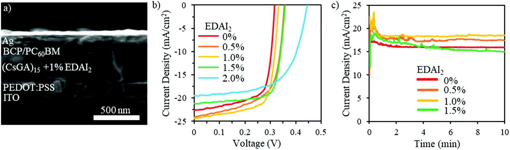 | ||
| Fig. 3 (a) Cross-sectional SEM image showing the (CsGA)15 + 1.0% EDAI2 PVSC with the following layers: ITO (200 nm)/PEDOT:PSS (50 nm)/perovskite (400 nm)/PC60BM/BCP/Ag (100 nm). (b) Photocurrent density–voltage (J–V) characteristics of the best performance PVSCs with the active layer containing (CsGA)15 + y% EDAI2 thin films with y = 0, 0.5, 1.0, 1.5, and 2.0 under AM 1.5G illumination scanned from −0.1 to 0.6 V at a scan rate of 0.01 V s−1. (c) Steady state photocurrent for the best performance PVSCs containing the active layers of (CsGA)15 at the maximum power points with the voltages of 0.274, 0.290, 0.272, and 0.308 V for 0, 0.5, 1.0, and 1.5% EDAI2, respectively. | ||
| Device | V oc (V) | J sc (mA cm2) | FF | PCE (%) | R s (Ω cm2) | R sllh (Ω cm2) |
|---|---|---|---|---|---|---|
| (CsGA)15 + 0% | 0.30 ± 0.02 (0.32) | 20.84 ± 3.31 (22.61) | 0.71 ± 0.01 (0.70) | 4.45 ± 0.87 (5.01) | 2.40 | 64.46 |
| (CsGA)15 + 0.5% | 0.35 ± 0.02 (0.35) | 21.43 ± 2.28 (24.03) | 0.61 ± 0.04 (0.63) | 4.58 ± 0.61 (5.39) | 4.22 | 66.59 |
| (CsGA)15 + 1.0% | 0.35 ± 0.02 (0.33) | 20.81 ± 1.78 (24.32) | 0.63 ± 0.06 (0.71) | 4.62 ± 0.63 (5.72) | 2.72 | 78.00 |
| (CsGA)15 + 1.5% | 0.38 ± 0.01 (0.36) | 20.23 ± 1.18(21.16) | 0.66 ± 0.06 (0.75) | 5.05 ± 0.53 (5.69) | 3.05 | 133.92 |
| (CsGA)15 + 2.0% | 0.43 ± 0.02 (0.45) | 15.20 ± 2.50 (19.53) | 0.57 ± 0.04 (0.62) | 3.74 ± 0.94 (5.40) | 6.67 | 92.14 |
A previous study has shown that devices based on GA0.20FA0.80SnI3 with 1% EDAI2 active layers exhibited a Voc of 0.619 V compared to 0.49 V for the devices based on FASnI3 with 1% EDAI2 active layers because of the downshifted valence band maximum to −5.20 eV versus −4.92 eV, which aligns better with the work function of PEDOT:PSS (−5.2 eV) as the HTL. The Voc values of our devices are low compared to the reported Voc values. To further investigate this, we conducted ultraviolet photoelectron spectroscopy (UPS) analysis of (CsGA)5, (CsGA)10 and (CsGA)15 films with 1.5% EDAI2 because the devices based on these films exhibit high performance. Fig. 4a shows the energy diagram of the materials involved in the devices. The valence band maxima (VBMs) of (CsGA)5, (CsGA)10 and (CsGA)15 with 1.5% EDAI2 were obtained from their UPS spectra (Fig. S8, ESI†) and the conduction band minima (CBMs) were estimated from the VBMs and the optical band gaps determined from the UV-Vis spectra of the (CsGA)5, (CsGA)10 and (CsGA)15 films with 1.0% EDAI2. The VBMs are determined to be −5.08, −5.07 and −5.16 eV for (CsGA)5, (CsGA)10 and (CsGA)15 with 1.5% EDAI2, respectively. All of them are unfavorable for hole transport with the PEDOT:PSS HTL,15 which could lead to low Voc values. The deepest VBM and the smallest band gap of (CsGA)15 make the CBM downshift to −3.73 eV. Both the downshifted VBM and CBM of (CsGA)15 enable the best energy alignment with the HTL and ETL, respectively, which could explain the best performance of devices based on (CsGA)15 films. The (CsGA)5, (CsGA)10 and (CsGA)15 films with 1.5% EDAI2 have a Fermi level 0.4 eV above the VBM, indicating the p-type doping of all these perovskites (Fig. 4b). Previous studies have shown that guanidinium addition in MAPbI3 converts the perovskite to a p-type semiconductor with the Fermi level shifting from 1.1 to 0.89 eV above the VBM for MAPbI3 and GA0.25MA0.75PbI3, respectively.37 X-site anion interstitial (Xi), A-site and B-site vacancy (VA and VB), and antisite (AB, XA and XB) point defects typically lead to p-type perovskites.21 Sn-based perovskites tend to be p-type due to self-doping by Sn4+.38 The p-type nature of the (CsGA)15 film with 1.5% EDAI2 could be due to EDAI2 having a “hollowing” impact on the perovskite structure, giving the increased lattice parameter (Fig. 2c). EDAI2 has been shown to favor replacing octahedral cages with the B-site and the X-site and these metal and halide defects (vacancies and antisites) contribute to a more p-type perovskite.19,29,39 Since the lattice parameters of (CsGA)5 and (CsGA)10 films with 1.5% EDAI2 are even smaller than those without EDAI2 because of the possibility of expelling GA+ cations, A-site vacancies could be formed in these perovskites besides the aforementioned point defects, resulting in p-type perovskites.
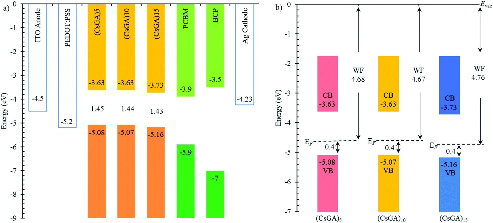 | ||
| Fig. 4 (a) Band energy diagram of PVSCs with (CsGA)x + 1.5% EDAI2 active layers, where x = 5, 10 and 15. The band gaps derived from the UV-Vis spectra are indicated. (b) Energy level scheme for the (CsGA)5, (CsGA)10 and (CsGA)15 films with 1.5% EDAI2 based on the parameters derived from the UPS spectra. | ||
Balanced charge generation, recombination and extraction rates are key factors in determining solar cell performance.40 Charge recombination results in loss of photogenerated charges, lowering Jsc and FF. The maximum Voc of a solar cell can be achieved when all photogenerated charges recombine solely radiatively.41 To understand device performance related to the mitigation of defects by incorporating EDAI2 in (CsGA)15 perovskites, we investigated the evolution of Voc, Jsc and FF as a function of light intensity for (CsGA)15 with 0–1.5% EDAI2. The Voc of light intensity is an independent exploration of recombination compared to that of Jsc and FF. The current is zero under open-circuit conditions with all photogenerated carriers recombining within the cell. Recombination studies near the open-circuit are, therefore, particularly sensitive to recombination mechanisms and the impact of shallow traps. The open-circuit voltage shows a logarithmic dependence on light intensity with a slope of nkBT/q, where n represents different recombination mechanisms, kB is the Boltzmann constant, T is the absolute temperature, and q is the elementary charge. When n > 2, monomolecular recombination dominates and trap states play a significant role, while when n ∼ 1, bimolecular recombination dominates, demonstrating minimal shallow trap states in the perovskites.42 The Vocversus logarithmic scale light intensity plots for (CsGA)15 devices show that the slope changes from greater than 2 to close to 1 from no EDAI2 addition to 1.0 and 1.5% EDAI2 addition (Fig. 5a), indicating charge carrier recombination from monomolecular, trap-state assisted recombination to biomolecular recombination. These results are consistent with the trap-state reduction shown by the UV-Vis and PL spectra, which further supports the hypothesis that EDAI2 has a hollowing effect, reducing bulk defects.
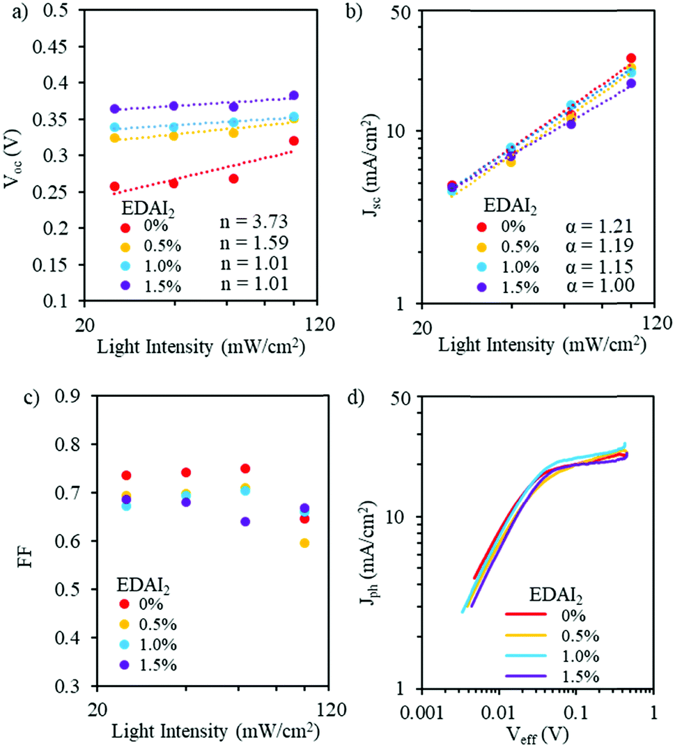 | ||
| Fig. 5 (a) Voc, (b) Jsc, and (c) FF as a function of light intensity and (d) photocurrent density as a function of effective voltage for PVSCs with (CsGA)15 + 0–1.5% EDAI2. | ||
Fig. 5b shows the double logarithmic scale with the relation of Jscversus light intensity. For the power law dependence of Jsc on light intensity (Jsc ∝ Iα), the deviation from unity of the slope implies bimolecular recombination. When α is less than 1, this could be a result of bimolecular recombination, variations in both carrier mobilities, or distribution in the density of states. When α ∼ 0.75, space charge effects might be induced by the interfacial layers. When α = 1, there are no space charge effects and all carriers are swept out prior to recombination.42,43 For EDAI2 addition from 0% to 1.5%, α values change from 1.21 to 1.00. This shows that the addition of EDAI2 reduces the deep trap states by passivating grain boundaries and charge carriers are effectively extracted. We also plotted FF as a function of logarithmic scale light intensity (Fig. 5c). These FF trends show the different capabilities of the perovskite materials to support balanced charge carrier generation and extraction over this range of light intensities. At low light intensities, the (CsGA)15 device without EDAI2 shows a higher FF compared to the devices with 0.5–1.5% EDAI2, indicating that, despite the trap states, low density charge carriers in (CsGA)15 + 0% EDAI2 are still able to be extracted due to the high intrinsic charge carrier mobility and long diffusion length of perovskites.44,45 When the light intensity increases to 1 sun, 100 mW cm−2, more charge carriers are recombined via trap states, leading to a significant decrease of FF for (CsGA)15 with 0 and 0.5% EDAI2. The (CsGA)15 device with 1.5% EDAI2 retains the same level of FF at 1 sun illumination, demonstrating the reduction of trap states by adding EDAI2. To elucidate whether the FF reduction under 1 sun illumination for the (CsGA)15 devices without EDAI2 and those with 0.5–1% EDAI2 is due to the charge extraction limit, we explored the photocurrent density (Jph) as a function of effective voltage (Veff). Jph is defined as Jph = J1 − Jd, where J1 and Jd represent the current densities under light and dark conditions, respectively. Veff is defined as Veff = V0 − V, where V0 is the compensation voltage defined as Jph(V0) = 0 and V is the applied voltage.40Fig. 5d shows that, for all devices, photocurrent densities under 1 sun illumination reach saturation at a similar low effective voltage ∼0.05 V, suggesting that charge extraction is not a limiting factor. The low saturation effective voltage could be linked to the better band alignment of (CsGA)15 with the charge selective layers (Fig. 4a).
To determine the impact of mixing CsGA with FA at the A-site and adding EDAI2 on the stability of pure Sn perovskite solar cells, long-term device stability in an inert environment was evaluated. Fig. 6 shows the normalized Voc, Jsc, FF, and PCE of (CsGA)15 + 0–1.5% EDAI2 devices over 45 days in an inert nitrogen atmosphere. The devices with 0% EDAI2 show a decrease of all photovoltaic parameters over time and after 30 days show a short-circuited behavior. This short-circuited behavior is due to highly oxidized Sn4+, which has been shown to create metal-like conductivity in perovskite solar cells.46 The addition of EDAI2 greatly increased the device stability, further demonstrating the point defect reducing capability of EDAI2 by hollowing crystal structures and passivating grain boundaries. In the case of 0.5–1.5% EDAI2 addition, Fig. 6 shows that Voc is very stable while Jsc and FF briefly increase during storage. The performance of the (CsGA)0.15FA0.70SnI3 device with 1.5% EDAI2 shows an increase in maximum PCE from 5.69% to 6.39% after 5 days of storage. Previously, with GA0.2FA0.8SnI3 perovskite films and 1% EDAI2, the efficiency also increased in storage as well.15 Since this phenomenon only occurs with EDAI2 addition in our research and mostly impacts Jsc, this shows that there is an increased amount of grain passivation over time. EDAI2 is successfully able to prevent oxidation, maintaining these photovoltaic parameters.
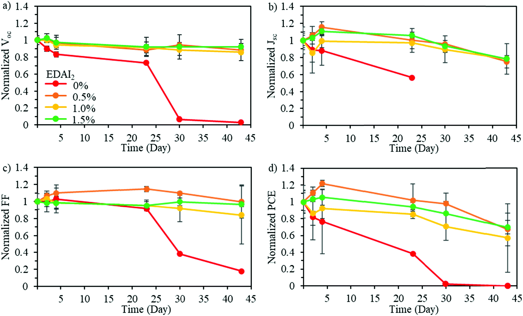 | ||
| Fig. 6 Normalized (a) Voc, (b) Jsc, (c) FF, and (d) PCE of the devices containing the active layers of (CsGA)15 + 0–1.5% EDAI2 over time in a nitrogen-filled glove box. The (CsGA)15 + 0% EDAI2 devices showed a short-circuited behavior after 30 days. | ||
Conclusion
In summary, the addition of Cs+ and GA+ into FASnI3 was implemented to utilize the high hydrogen bonding capability of the GA+ organic cation while relaxing the local lattice strain and filling point defects with a smaller Cs+ counter cation. The EDAI2 additive not only yielded pinhole-free cubic phase (CsGA)xFA1−2xSnI3 perovskite films but also decreased both shallow and deep trap states in the perovskite films. With increased CsGA substitution, the relaxed strain allowed more integration of EDAI2 into the crystal structure, increasing these positive impacts. The devices with (CsGA)0.15FA0.70SnI3 and 0–2% EDAI2 all achieved a maximum PCE higher than 5% with the highest of 5.72% for a fresh device with (CsGA)0.15FA0.70SnI3 and 1% EDAI2. After storage, the maximum PCE was increased from 5.69% to 6.39% for the (CsGA)0.15FA0.70SnI3 and 1.5% EDAI2 devices. The devices with the EDAI2 additive showed better long-term stability compared to those without EDAI2. Overall, this study demonstrates cation tuning to integrate stabilizing factors into pure Sn perovskites, creating potential routes for further improving lead-free devices in the future.Conflicts of interest
The authors declare no conflict of interest.Acknowledgements
This work was supported by the National Science Foundation (NSF) (CBET-1748101 and CMMI-1661660) and the Defense Threat Reduction Agency (HDTRA 1-15-1-0021). GAT acknowledges the support from the NSF Graduate Research Fellowship Program Fellowship and the University of Washington (UW) Clean Energy Institute (CEI) Graduate Research and Education Fellowships funded by the State of Washington via the Washington Research Foundation. Part of this work was conducted at the Molecular Analysis Facility, a National Nanotechnology Coordinated Infrastructure site at the UW, which is supported in part by the NSF (ECC-1542101), the UW, the Molecular Engineering & Sciences Institute, the CEI, and the National Institutes of Health. Some device fabrications and evaluations were carried out in the UW Department of Chemistry's Photonics Research Center. UV-Vis-NIR absorption measurements were carried out in the UW Department of Chemistry's Spectroscopic and Analytical Instrumentation facility.References
- NREL, Best Research-Cell Efficiency Chart, https://www.nrel.gov/pv/cell-efficiency.html.
- Q. Chen, N. De Marco, Y. Yang, T. Bin Song, C. C. Chen, H. Zhao, Z. Hong, H. Zhou and Y. Yang, Nano Today, 2015, 10, 355–396 CrossRef CAS.
- S. Chatterjee and A. J. Pal, J. Mater. Chem. A, 2018, 6, 3793–3823 RSC.
- G. Nasti and A. Abate, Adv. Energy Mater., 2019, 13, 1–16 Search PubMed.
- H. Yao, F. Zhou, Z. Li, Z. Ci, L. Ding and Z. Jin, Adv. Sci., 2020, 1903540 CrossRef CAS.
- K. Liang, D. B. Mitzi and M. T. Prikas, Chem. Mater., 1998, 10, 403–411 CrossRef CAS.
- T. Leijtens, R. Prasanna, A. Gold-Parker, M. F. Toney and M. D. McGehee, ACS Energy Lett., 2017, 2, 2159–2165 CrossRef CAS.
- W. Ke and M. G. Kanatzidis, Nat. Commun., 2019, 10, 1–4 CrossRef CAS.
- C. C. Stoumpos, C. D. Malliakas and M. G. Kanatzidis, Inorg. Chem., 2013, 52, 9019–9038 CrossRef CAS.
- M. Konstantakou and T. Stergiopoulos, J. Mater. Chem. A, 2017, 5, 11518–11549 RSC.
- Z. Chen, C. Yu, K. Shum, J. J. Wang, W. Pfenninger, N. Vockic, J. Midgley and J. T. Kenney, J. Lumin., 2012, 132, 345–349 CrossRef CAS.
- N. K. Noel, S. D. Stranks, A. Abate, C. Wehrenfennig, S. Guarnera, A. A. Haghighirad, A. Sadhanala, G. E. Eperon, S. K. Pathak, M. B. Johnston, A. Petrozza, L. M. Herz and H. J. Snaith, Energy Environ. Sci., 2014, 7, 3061–3068 RSC.
- F. Hao, C. C. Stoumpos, D. H. Cao, R. P. H. Chang and M. G. Kanatzidis, Nat. Photonics, 2014, 8, 489–494 CrossRef CAS.
- W. Liao, D. Zhao, Y. Yu, C. R. Grice, C. Wang, A. J. Cimaroli, P. Schulz, W. Meng, K. Zhu, R. G. Xiong and Y. Yan, Adv. Mater., 2016, 28, 9333–9340 CrossRef CAS.
- E. Jokar, C. H. Chien, C. M. Tsai, A. Fathi and E. W. G. Diau, Adv. Mater., 2019, 31, 1–7 CrossRef.
- S. Kanno, Y. Imamura and M. Hada, J. Phys. Chem. C, 2018, 122, 15966–15972 CrossRef CAS.
- N. De Marco, H. Zhou, Q. Chen, P. Sun, Z. Liu, L. Meng, E. P. Yao, Y. Liu, A. Schiffer and Y. Yang, Nano Lett., 2016, 16, 1009–1016 CrossRef.
- M. I. Saidaminov, J. Kim, A. Jain, R. Quintero-Bermudez, H. Tan, G. Long, F. Tan, A. Johnston, Y. Zhao, O. Voznyy and E. H. Sargent, Nat. Energy, 2018, 3, 648–654 CrossRef CAS.
- W. Ke, C. C. Stoumpos, M. Zhu, L. Mao, I. Spanopoulos, J. Liu, O. Y. Kontsevoi, M. Chen, D. Sarma, Y. Zhang, M. R. Wasielewski and M. G. Kanatzidis, Sci. Adv., 2017, 3, 1–10 Search PubMed.
- Z. Ni, C. Bao, Y. Liu, Q. Jiang, W. Q. Wu, S. Chen, X. Dai, B. Chen, B. Hartweg, Z. Yu, Z. Holman and J. Huang, Science, 2020, 367, 1352–1358 CrossRef CAS.
- H. Jin, E. Debroye, M. Keshavarz, I. G. Scheblykin, M. B. J. Roeffaers, J. Hofkens and J. A. Steele, Mater. Horiz., 2020, 7, 397–410 RSC.
- I. Spanopoulos, W. Ke, C. C. Stoumpos, E. C. Schueller, O. Y. Kontsevoi, R. Seshadri and M. G. Kanatzidis, J. Am. Chem. Soc., 2018, 140, 5728–5742 CrossRef CAS.
- E. Jokar, C. H. Chien, A. Fathi, M. Rameez, Y. H. Chang and E. W. G. Diau, Energy Environ. Sci., 2018, 11, 2353–2362 RSC.
- S. J. Lee, S. S. Shin, Y. C. Kim, D. Kim, T. K. Ahn, J. H. Noh, J. Seo and S. Il Seok, J. Am. Chem. Soc., 2016, 138, 3974–3977 CrossRef CAS.
- T. Bin Song, T. Yokoyama, S. Aramaki and M. G. Kanatzidis, ACS Energy Lett., 2017, 2, 897–903 CrossRef.
- T. Wang and F. Yan, Chem. – Asian J., 2020, 15, 1524–1535 CrossRef CAS.
- Z. Zhu, C. C. Chueh, N. Li, C. Mao and A. K. Y. Jen, Adv. Mater., 2018, 30, 1–9 Search PubMed.
- Q. Q. Ge, J. Ding, J. Liu, J. Y. Ma, Y. X. Chen, X. X. Gao, L. J. Wan and J. S. Hu, J. Mater. Chem. A, 2016, 4, 13458–13467 RSC.
- W. Ke, I. Spanopoulos, Q. Tu, I. Hadar, X. Li, G. S. Shekhawat, V. P. Dravid and M. G. Kanatzidis, J. Am. Chem. Soc., 2019, 141, 8627–8637 CrossRef CAS.
- D. J. Kubicki, D. Prochowicz, A. Hofstetter, M. Saski, P. Yadav, D. Bi, N. Pellet, J. Lewiński, S. M. Zakeeruddin, M. Grätzel and L. Emsley, J. Am. Chem. Soc., 2018, 140, 3345–3351 CrossRef CAS.
- W. Zhang, J. Xiong, J. Li and W. A. Daoud, J. Mater. Chem. A, 2019, 7, 9486–9496 RSC.
- K. Huang, L. Yuan and S. Feng, Inorg. Chem. Front., 2015, 2, 965–981 RSC.
- G. A. Tosado, Y. Y. Lin, E. Zheng and Q. Yu, J. Mater. Chem. A, 2018, 6, 17426–17436 RSC.
- J. H. Lee, N. C. Bristowe, J. H. Lee, S. H. Lee, P. D. Bristowe, A. K. Cheetham and H. M. Jang, Chem. Mater., 2016, 28, 4259–4266 CrossRef CAS.
- R. Prasanna, A. Gold-Parker, T. Leijtens, B. Conings, A. Babayigit, H. G. Boyen, M. F. Toney and M. D. McGehee, J. Am. Chem. Soc., 2017, 139, 11117–11124 CrossRef CAS.
- Y. Shao, Z. Xiao, C. Bi, Y. Yuan and J. Huang, Nat. Commun., 2014, 5, 1–7 Search PubMed.
- D. Prochowicz, M. M. Tavakoli, A. Q. Alanazi, S. Trivedi, H. Tavakoli Dastjerdi, S. M. Zakeeruddin, M. Grätzel and P. Yadav, ACS Omega, 2019, 4, 16840–16846 CrossRef CAS.
- E. W. G. Diau, E. Jokar and M. Rameez, ACS Energy Lett., 2019, 4, 1930–1937 CrossRef CAS.
- W. Ke, C. C. Stoumpos, I. Spanopoulos, L. Mao, M. Chen, M. R. Wasielewski and M. G. Kanatzidis, J. Am. Chem. Soc., 2017, 139, 14800–14806 CrossRef CAS.
- J. Troughton, N. Gasparini and D. Baran, J. Mater. Chem. A, 2018, 6, 21913–21917 RSC.
- W. Shockley and H. J. Queisser, J. Appl. Phys., 1961, 32, 510–519 CrossRef CAS.
- S. R. Cowan, A. Roy and A. J. Heeger, Phys. Rev. B: Condens. Matter Mater. Phys., 2010, 82, 1–10 CrossRef.
- S. Shao, Z. Chen, H. H. Fang, G. H. Ten Brink, D. Bartesaghi, S. Adjokatse, L. J. A. Koster, B. J. Kooi, A. Facchetti and M. A. Loi, J. Mater. Chem. A, 2016, 4, 2419–2426 RSC.
- L. M. Herz, ACS Energy Lett., 2017, 2, 1539–1548 CrossRef CAS.
- S. D. Stranks, G. E. Eperon, G. Grancini, C. Menelaou, M. J. P. Alcocer, T. Leijtens, L. M. Herz, A. Petrozza and H. J. Snaith, Science, 2013, 342, 341–345 CrossRef CAS.
- I. Chung, J. H. Song, J. Im, J. Androulakis, C. D. Malliakas, H. Li, A. J. Freeman, J. T. Kenney and M. G. Kanatzidis, J. Am. Chem. Soc., 2012, 134, 8579–8587 CrossRef CAS.
Footnote |
| † Electronic supplementary information (ESI) available. See DOI: 10.1039/d0ma00520g |
| This journal is © The Royal Society of Chemistry 2020 |