
 Open Access Article
 This Open Access Article is licensed under a Creative Commons Attribution-Non Commercial 3.0 Unported Licence
Transport mechanism of copper sulfide embedded carbon nitride thin films: a formation free memristor†
Venkata K.
Perla
,
Sarit K.
Ghosh
and
Kaushik
Mallick
 *
*
Department of Chemical Sciences, University of Johannesburg, P.O. Box: 524, Auckland Park 2006, South Africa. E-mail: kaushikm@uj.ac.za
First published on 14th April 2020
Abstract
Nonvolatile electrical resistive behaviour was demonstrated for a copper sulfide nanoparticle decorated carbon nitride (CSCN) based device. The copper sulfide–carbon nitride composite system was synthesized using a high temperature in situ protocol, where the sulfide particles were highly dispersed on the carbon nitride matrix. The CSCN composite was characterized by using different analytical techniques. The transport mechanism of the device followed Poole–Frenkel (PF) for the OFF-state, whereas ohmic behaviour dominated for the ON-state. An endurance study of the device was performed with a duty-cycle of 50% for 2 × 10³ cycles and the nonvolatile behavior of the device was studied with a duty-cycle of 0.16% for 2 × 10³ s. Both the endurance and nonvolatile behavior exhibited excellent stability of the device with an ON to OFF ratio of 104.
1. Introduction
Nonvolatile resistive memory has attracted significant attention for next-generation data-storage applications1,2 due to faster device performance, data nonvolatility and low power consumption.3,4 A resistive memory device utilizes the bistable resistances of the high-resistance state and low-resistance state of materials.5 The simple architectural design also makes a resistive memory device more attractive over other memory candidates, such as ferroelectric and magnetoresistive memory devices.6,7 Resistive switching between the high-resistance state and low-resistance state has been observed in a large variety of materials, including transition metal oxides,8 post-transition metal oxides,9 perovskite materials,10 organic materials11 and organic–inorganic hybrid systems12 with a metal–insulator–metal structure.Among the various transition metals, copper based materials have been studied extensively for resistive memory applications. A device made with copper sulphide (Ti–Cu2S–Cu) exhibited bipolar resistive switching behaviour with an ON–OFF ratio of 0.20 × 102,13 whereas another copper sulphide based device with a different electrode combination (Pt–Cu2S–Pt) exhibited resistive switching behaviour with an ON–OFF ratio of 102.14 The electrical bistability of a reported device made with an active component of a Cu2FeSnS4 thin film, sandwiched between ITO and Al-electrodes, displayed bipolar-type current–voltage characteristics with an ON–OFF ratio of 103.15 Highly oriented Cu2O films showed a unipolar resistive switching phenomenon, originating from the creation of metallic filaments due to the O2− generation and the O2 gas evolution.16 A copper oxide based resistive switching memory device, for electronic textile applications, showed a switching ratio of 102 between the high and low resistance states where the two stable states were retained for 107 seconds.17 Bipolar switching behavior was reported18 for the graphene–copper oxide system and the switching behavior was controlled by the migration of oxygen ions from the copper oxide layer. Based on two separate experiments, it was reported19 that the junction properties of a Ti–CuO–Cu device displayed two different transport characteristics when the active layer was combined with an organic material. The hybrid system of CuO and hexa-peri-hexabenzocoronene (HBC) exhibited unipolar switching behavior, whereas on replacing HBC with a fluorine derivative of HBC (hexafluoro-hexa-peri-hexabenzocoronene) bipolar resistive switching was observed. It was assumed that the incorporation of a strong-electron withdrawing fluorine component plays a significant role in the electronic properties of the device. The incorporation of a CuO layer with the ZnO layer in a Cu–ZnO–AZO (Al-doped ZnO) based device showed improved switching performance compared to the ZnO based single layer system. The conduction behaviour of the high and low resistance states followed trap-controlled space charge limited current (SCLC) and ohmic mechanisms, respectively, and the CuO layer served as the reservoir and supplier of oxygen ions in the SET and RESET process, respectively, which played a critical role for the forming and rupture of the filament.20 Copper oxide nano-wires21 and nanodots22 showed formation induced resistive switching behaviour due to the copper ion migration. A device made with a copper sulfide thin film, sandwiched between a copper and another metal electrode (Au/Pt/Ti), demonstrated the effect of nonvolatile memory. The resistive switching process was explained by the formation and disruption of a conducting path, created due to the copper ion migration from the Cu-electrode to the copper sulfide film.23
Graphitic carbon nitride, which is composed of carbon and nitrogen, can be easily synthesized under thermal condensation and has lots of advantages, such as moderate bandgap, non-toxic nature, high surface area, and stability in the atmospheric environment and also at high temperature. Due to these merits, carbon nitride (CN) has been applied as a support material for a wide-range of inorganic nanomaterials for diverse applications.24 However, the application of carbon nitride for the fabrication of resistive random-access memory (RRAM) devices has rarely been reported. A device made with CN powder, as an active layer, was reported for RRAM applications with a switching ratio <100.25 A further report on CN for RRAM applications has been published where a CN in combination with poly-methyl methacrylate based device (Al–PMMA–CN–PMMA–ITO) exhibited typical bipolar resistive switching behavior with an ON-to-OFF ratio of 103.26
In this study, a high temperature in situ protocol was adopted to synthesise a copper sulfide nanoparticle decorated carbon nitride based thin composite film, where thiourea and copper nitrate were used as the precursors. The CSCN hybrid system was used as an active material for resistive random-access memory applications. The endurance and nonvolatile behavior of the device were studied for 2 × 10³ cycles and for 2 × 10³ s, respectively.
2. Experiment
2.1. Materials
Analytical grade chemicals were used in this investigation without further purification.2.2. Preparation of the carbon nitride stabilized copper sulfide composite system (CSCN)
A mixture of copper nitrate, Cu(NO3)2·3H2O, and thiourea, CS(NH2)2, in a ratio of 1![[thin space (1/6-em)]](https://www.rsc.org/images/entities/char_2009.gif) :5 (by weight), respectively, was kept inside a programmable furnace at 550 °C for 4 h and cooled down to room temperature. A constant argon atmosphere was maintained in the furnace during the synthesis process by continuous purging of argon gas. A dark brown coloured solid power CSCN (a) was recovered from the reaction chamber and characterized using different techniques. Two other samples, CSCN (b) and CSCN (c), were prepared under identical reaction conditions as above, using a copper nitrate and thiourea composition ratio of 0.5:5 and 2:5 (by weight), respectively. The formation mechanism of CSCN is schematically represented in Scheme 1.
:5 (by weight), respectively, was kept inside a programmable furnace at 550 °C for 4 h and cooled down to room temperature. A constant argon atmosphere was maintained in the furnace during the synthesis process by continuous purging of argon gas. A dark brown coloured solid power CSCN (a) was recovered from the reaction chamber and characterized using different techniques. Two other samples, CSCN (b) and CSCN (c), were prepared under identical reaction conditions as above, using a copper nitrate and thiourea composition ratio of 0.5:5 and 2:5 (by weight), respectively. The formation mechanism of CSCN is schematically represented in Scheme 1.
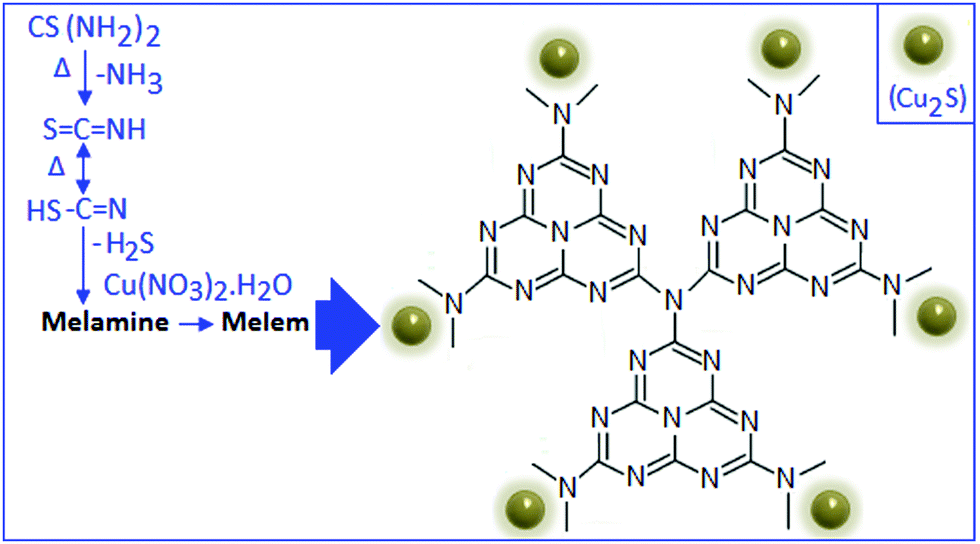 | ||
| Scheme 1 The formation mechanism of embedded copper sulfide in the carbon nitride matrix. | ||
2.3. Device fabrication and electrical characterization
Glass slide supported flexible paper was used for the device fabrication, where the role of the slide was to provide mechanical strength. The CSCN (a) material was ground thoroughly and made into a slurry with methanol. The CSCN based slurry was dispersed in the form of a thin film on previously deposited bottom electrodes (gold) on the flexible paper using the spin coating technique. After proper drying, the top gold electrodes were deposited in a cross-bar fashion and a sandwich structured device was fabricated (Au||CSCN||Au). Fig. S1 inset (A) shows the schematic diagram of the cross-section image of the fabricated device (ESI†). The thickness of the fabricated Au-electrodes and the CSCN-layer is 200 nm and 0.5 μm, respectively. In a similar fashion, two other devices were fabricated using the samples CSCN (b) and CSCN (c).The bottom electrode was connected to the high voltage terminal whereas the top electrode was connected to the ground terminal of the electrical characterization unit. The current–voltage (I–V) measurement was performed with a 0.17 V s−1 scan rate and 0.1 V step size. Keithley 2401 and 2612B source meters were used for the electrical characterization.
3. Results and discussion
The structural pattern and stoichiometry composition of the Cu–S system depend on the thermodynamics and kinetics of the solid state reaction.27 The phase of the synthesized products was characterized by XRD analysis and the spectrum was recorded within the range (2θ) from 20° to 80°. The X-ray diffraction pattern (Fig. 1A) of Cu–S revealed that the majority of the diffraction peaks belong to the non-stoichiometric rhombohedral phase of Cu1.8S (JCPDS: 851693, green bar) with a lattice constant of a = b = c = 5.55 Å, whereas some of the diffraction peaks are matched with the hexagonal pattern of the Cu2S component (JCPDS: 840209, red bar). In the copper sulfide system, sulphur has a higher diffusion coefficient than copper, which results the formation of nonstoichiometric Cu2−xS structure.28,29 In the XRD pattern, the most intense peak can be indexed as the interlayer spacing of the stacked aromatic segments in the (002) planes with a distance of 0.324 nm of the conjugated aromatic ring with lattice constant values of a = b = 4.72 Å and c = 6.72 Å derived from the hexagonal (P6m2) phase of graphitic carbon nitride (JCPDS: 871526)30 at 27° and also as the Cu2S particles originating from the same (002) plane at 26.18°.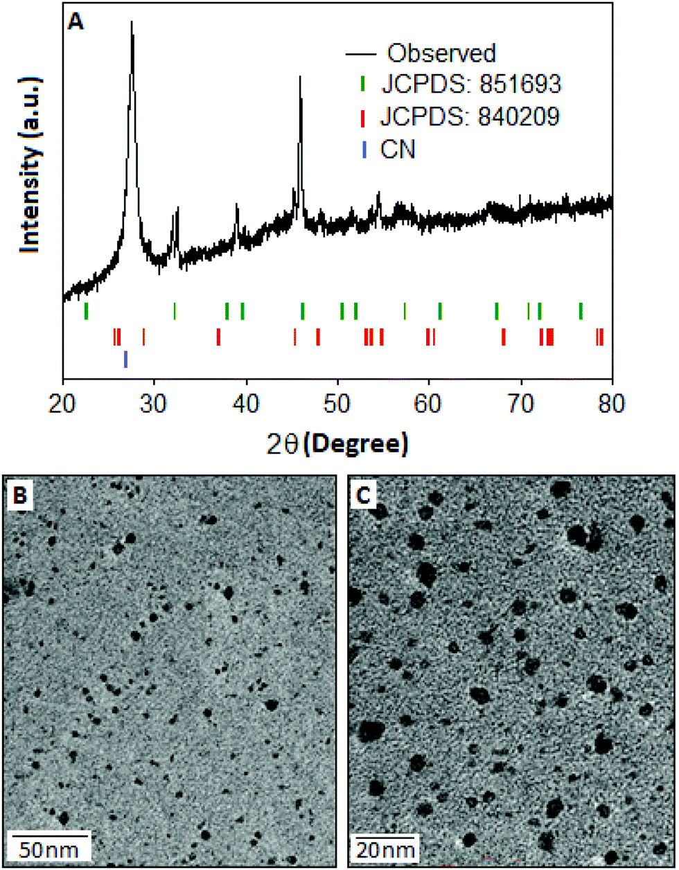 | ||
| Fig. 1 (A) X-ray diffraction pattern of Cu2−xS particles embedded within the carbon nitride matrix. The pattern consists of mixed phases of Cu1.8S (green bar, JCPDS: 851693) and Cu2S (red bar, JCPDS: 840209) compositions. The hexagonal phase of carbon nitride (blue bar) is identified in the diffraction pattern. (B and C) TEM images of copper sulfide nanoparticles on the carbon nitride matrix, with different magnification. | ||
The TEM images of CSCN are shown in Fig. 1(B and C) with different magnifications. Copper sulfide nanoparticles (dark spots), with large size distribution, within the range of 2–10 nm, are observed on the carbon nitride matrix. The surface elemental composition and the electronic states of the copper sulfide were characterized by the X-ray photoelectron spectroscopy (XPS) technique. The copper (Cu) spectra (Fig. 2A) are well fitted with Cu 2p3/2 and Cu 2p1/2 located at 933.91 and 953.82 eV respectively. Two other peaks positioned at 942.2 eV and 962.3 eV could be assigned as shake-up peaks for Cu 2p3/2 and 2p1/2, respectively. After deconvolution of the peak located at 933.91 eV, two separate peaks at 933.55 and 935.50 eV were generated (Fig. 2A, inset), which indicate the presence of copper species in the form of Cu(I) and Cu(II), respectively,31 with different levels of concentration. Apart from the copper peaks, the material showed characteristic sulfur peaks positioned at 158.73 and 164.0 eV, Fig. 2B, assigned to S 2p3/2 and S 2p1/2, respectively.32
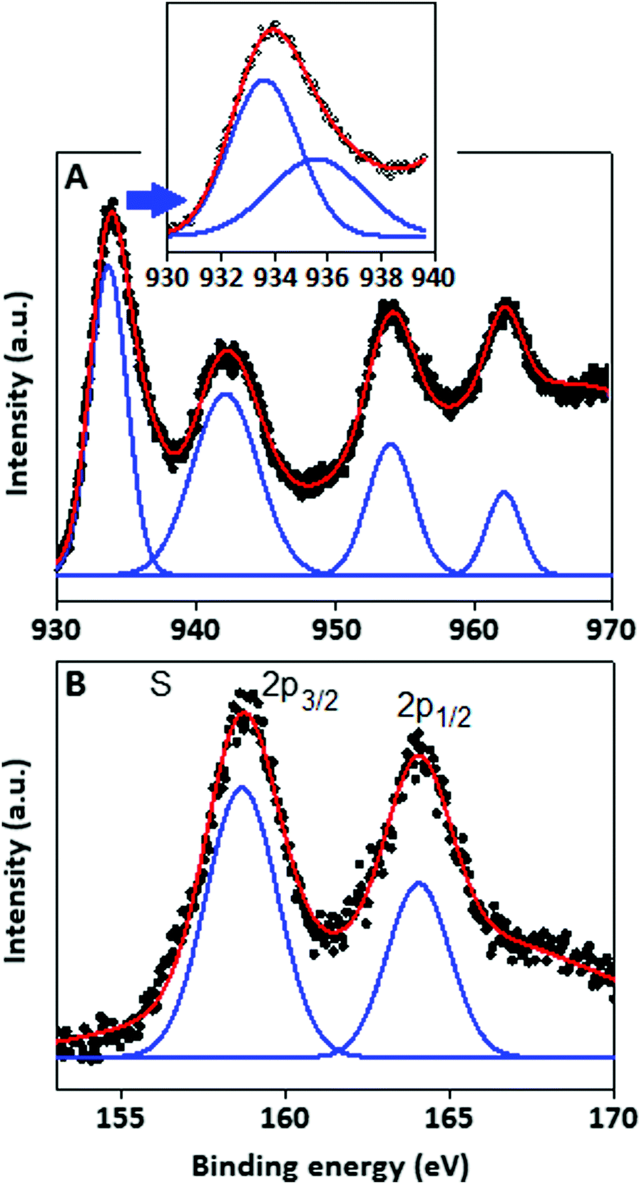 | ||
| Fig. 2 X-ray photoelectron spectroscopy characteristics of the copper sulfide particles. XPS signal for (A) copper species and (B) sulphur species. | ||
The electrical property of the device is displayed in Fig. 3 (main panel). The schematic diagram of the device is presented in Fig. 3A. During the voltage sweep from +5 to −5 V, the device exhibited the SET process (the current value shifts from the low to the high conductance state) at −2.9 V. Again, when the voltage sweep was from −5 to +5 V, the device exhibited the RESET process (the current value shifts from the high to the low conductance state) at 3.8 V. The device has been defined as bipolar as the SET and RESET process occurred at the opposite polarity (voltage). The endurance study of the device for multiple voltage sweeps is documented in the ESI† (Fig. S2). After the fourth cycle the device reached the stable form. The maximum ON–OFF ratio was achieved at −1.0 V and was 104. The device made with CSCN (c) exhibited a higher conduction state, Fig. 3B(I), black in colour, as compared with the device made with CSCN (b), Fig. 3B(II), red in colour. For both the devices no resistive switching effect was observed. The above phenomenon can be explained by the amount of copper sulfide particle formation. The higher conductance state indicates that nanoparticles played a major role in the conduction process, whereas the low conductance state suggests that carbon nitride contributes the charge transport process.
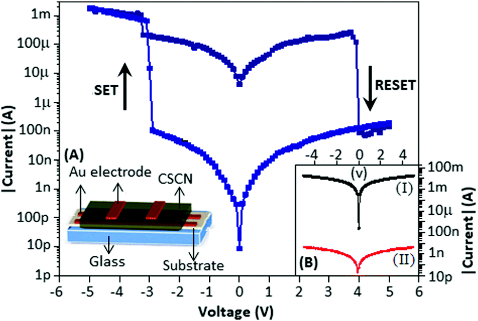 | ||
| Fig. 3 Semi-log current–voltage (I–V) characteristics of the DUT, Au||CSCN||Au is bipolar in nature (main panel). Inset (A): Cross-bar structure of the Au||CSCN||Au device. Inset (B): Semi-log I–V of 0.5:5 and 2:5 of copper nitrate to thiourea (by wt) compositions. | ||
To understand the switching mechanism of the device, the current–voltage graph was fitted with different theoretical models for both the high conductance (ON) and low conductance (OFF) states. Fig. 4 shows the I–V characteristics on a double logarithmic scale, ln(I) vs. ln(V), where the low conductance state and high conductance state followed Poole–Frenkel (PF) and ohmic conduction mechanisms, respectively. From the graph, it is clear that during the voltage sweep from +5 to −5 V, the conductive path changed from PF to ohmic at −2.9 V (SET), whereas during the voltage sweep from −5 to +5 V, the conductive path changed from ohmic to PF at 3.8 V (RESET).
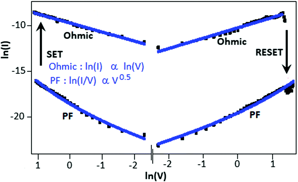 | ||
| Fig. 4 The current–voltage graph (log-scale) of the Au||CSCN||Au device exhibited Poole–Frenkel emission for the low conductance state and the ohmic mechanism for the high conductance state. | ||
The graphical representation of the current–voltage characteristic, in a linear form, is incorporated in the supplementary information, with realization of the PF and ohmic behaviour (Fig. S1, main panel, ESI†).
The energy diagram of the device (Fig. 5A) explains the transport mechanism on the basis of different energy of states.33–35 Initially the electrons are trapped and localized on carbon nitride and under a suitable potential the trapped electrons are released and move slowly from the valence band (VB) to the conduction band (CB) of the carbon nitride. The conduction band electrons migrate to the conduction band of copper sulfide. The transport of conduction band electrons among the copper sulfide particles follows the ohmic conduction mechanism (slope ∼ 0.96), where the current is linearly dependent on the electric field (Fig. 5B). The devices CSCN (b) and CSCN (c) follow the PF and ohmic type transport mechanisms, respectively.
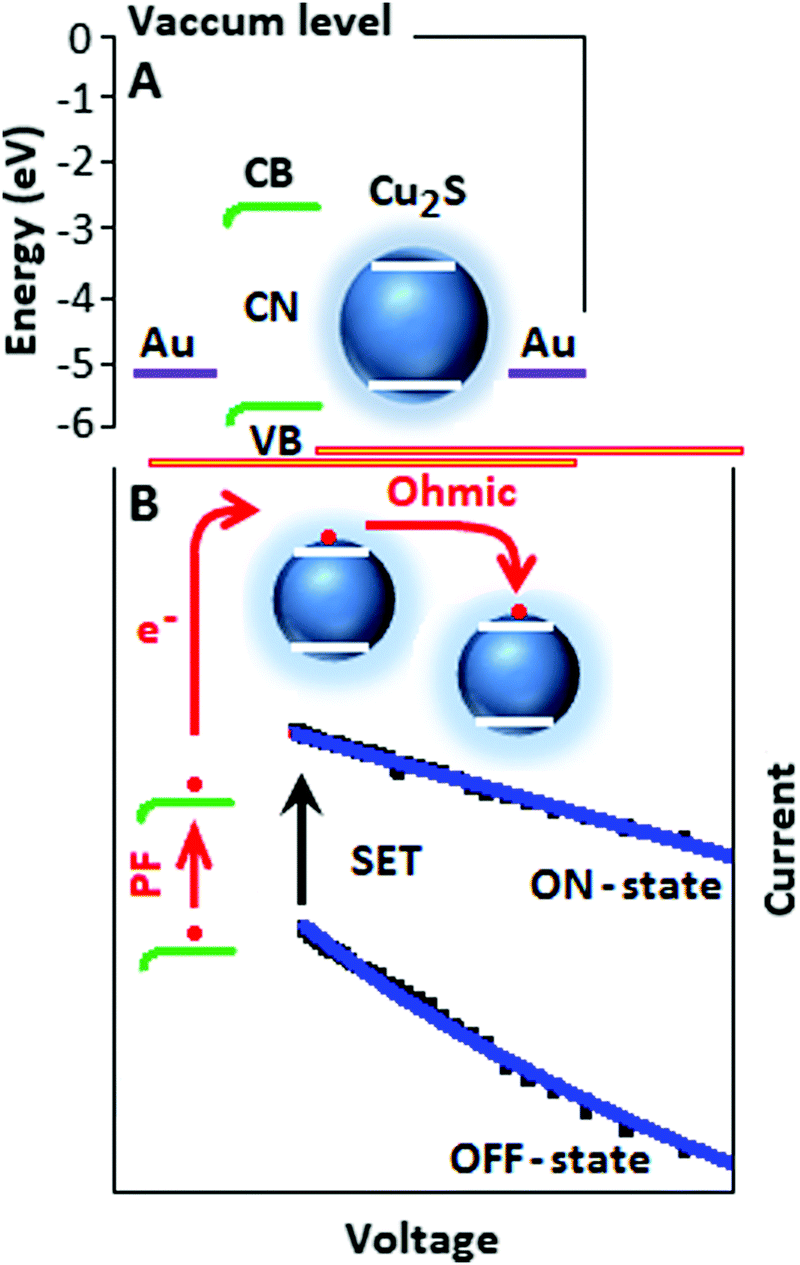 | ||
| Fig. 5 (A) The energy diagram of the Au||CSCN||Au device. (B) The electron transport mechanism within the device. The electron transfer, from the HOMO to the LUMO of the CN system, followed Poole–Frenkel emission for the OFF-state and the ohmic mechanism was followed for the ON-state through the Cu2S particles. | ||
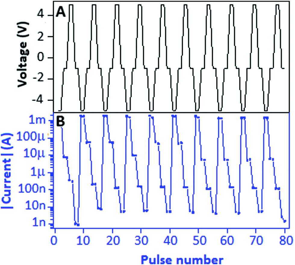
The properties of memory devices are mainly based on three major factors: the (a) endurance property, (b) nonvolatile property and (c) electrically rewritable property. For the endurance study, initially the device was exposed to +5 V and −5 V for a few seconds to imprint the low conductance state and high conductance state, respectively. The device was subjected to a pulse train consisting of −1 V for a 0.1 s time period separated by 0.1 s (Fig. 6A, inset) to investigate the stability of the device for the high conductance and low conductance states. In this experiment, the endurance study was carried out for 2 × 10³ cycles and Fig. 6A shows that both the high and low conductance states are moderately stable with an ON–OFF ratio of 104, which is comparable with the ON–OFF ratio achieved from the I–V curve (Fig. 3, main panel). Nonvolatile behaviour of the device is one of the major advantages of resistive switching memory devices. The nonvolatile study investigates the stability of the data retained within the DUT irrespective of the refreshing power supply. Prior to conducting the nonvolatile study, −5 V and +5 V were applied to the device for a few seconds to imprint the high and low conductance state, respectively. For the nonvolatile study, −1 V pulses for a 0.1 s time period, separated by 60 s, were applied to the device, Fig. 6B, inset (i). The duty cycle of each pulse was 0.16% in the pulse train. The device exhibited nonvolatile behavior (the states neither alter nor fluctuate) throughout the study for 2 × 10³ s with an ON–OFF ratio of above 104. Fig. 6(B) inset (ii) shows the proposed retention of the device with an estimable ON-to-OFF ratio of ∼104 after 107 s, by using the graphical extrapolation technique.36
 | ||
| Fig. 6 (A) The endurance study of the device for 2 × 10³ cycles. The pulse train employed for the endurance study (inset). (B) The nonvolatile study of the device for 2 × 10³ s. The pulse train employed for the nonvolatile study with a duty cycle of 0.16%, inset (i). The estimated retention of the device after 107 s, inset (ii). | ||
To study the electrically rewritable property, a Write–Read (1)–Erase–Read (0) (WR1ER0) cycle was designed to investigate the ability of the device for differentiating the low conductance state (0) from the high conductance state (1) after the erasing and writing process, respectively. WR1ER0 consists of four pulses of −5 V, −1 V, +5 V and −1 V corresponding to the Write, Read (1), Erase and Read (0) process of the device as shown in Fig. 7A. The current response of the WR1ER0 cycle is plotted on a semi-log scale (Fig. 7B), which exhibits a clear difference from Read (1) to Read (0) with a value of ∼10 μA. The current response (linear) is documented in Fig. S3(b), ESI.† The endurance, nonvolatile and electrically rewritable properties of the copper sulfide nanoparticle doped carbon nitride based hybrid device displayed competence for nonvolatile, bistable memory applications. As a ready reference for the readers, some copper based RRAM devices with parameters such as device structure, mechanism, ON-to-OFF ratio, endurance and retention are incorporated in this manuscript in a tabular form (Table 1).
 | ||
| Fig. 7 (A) The Write–Read (1)–Erase–Read (0) voltage cycle (−5.0, −1.0, +5.0 and −1.0 V) applied to the device and (B) the respective current response (semi-log scale) received from the device. | ||
| Material (M) | Device structure | Mechanism | ON–OFF ratio | Endurance | Retention | Ref. |
|---|---|---|---|---|---|---|
| SCLC: space-charge limited conduction, PF: Poole Frenkel, SE: Schottky emission, TE: thermionic emission, VRH: Mott's variable range hopping, p-ASA: poly-aminosalicylic acid. | ||||||
| Cu2S | Ti/M/Cu | NA | 0.2 × 10² | NA | NA | 13 |
| Cu2S | Pt/M/Pt | NA | 102 | NA | NA | 14 |
| Cu2FeSnS4 | ITO/M/AL | NA | 103 | NA | NA | 15 |
| CuS/Cu2−xS | FTO/M/Al | Ohmic, SCLC | 102 | 102 | NA | 37 |
| p-ASA–Cu | Au/M/Au | PF, ohmic | 2 × 10³ | 103 | 103 | 12 |
| CuxO | Cu/M/Ag | NA | 102 | NA | NA | 38 |
| CuxO | Al/M/Cu | NA | 103 | >102 | NA | 39 |
| CuOx | Ni/M/Ni | Ohmic, PF | 101 | 102 | 104 | 40 |
| CuO | Al/M/ITO | Ohmic, SCLC, TCLC | 105 | 2 × 10² | 104 | 41 |
| CuO | Al/M/ITO | Ohmic, SCLC | 103 | 2 × 10² | 104 | 42 |
| CuxO | KCu7S4/M/Au | Ohmic | 102 | 2 × 101 | 4 × 10² | 43 |
| CuO/Nb:SrTiO3 | Ag/M/Ag | NA | 102 | NA | NA | 44 |
| Cu2O | TiW/M/Cu | SE, VRH | 102 | NA | NA | 45 |
| CuxO | Au/Al/M/Au | SE, PF | 50 | 50 | NA | 46 |
| CSCN | Au/M/Au | Ohmic, PF | >104 | 2 × 10³ | 2 × 10³ | Present work |
4. Conclusion
A copper sulfide nanoparticle doped carbon nitride composite was synthesized using a high temperature in situ protocol, where the sulfide particles are highly dispersed within the carbon nitride matrix. To the best of our knowledge, this is the first kind of report where an in situ method has been applied for the simultaneous synthesis of carbon nitride and copper sulfide nanoparticles. The XRD and XPS analysis revealed the formation of nonstoichiometric copper sulfide and the TEM images displayed a large size distribution of the copper sulfide nanoparticles, within the range of 2–10 nm, on the carbon nitride matrix. The device exhibited bipolar characteristics for the resistive switching process where the low conductance state followed a Poole–Frenkel and the entire high conductance state followed an ohmic conduction mechanism. The device displayed excellent endurance and nonvolatile behaviour for 2 × 10³ cycles and 2 × 10³ s, respectively, and maintained a stable ON–OFF ratio of 104 for both. The electrically rewritable property clearly exhibited a difference among the Write, Read (1), Erase and Read (0) processes, which indicates that the device has the capability to process binary information for memory applications.Conflicts of interest
There are no conflicts to declare.Acknowledgements
This study was financially supported by the Faculty of Science and the Global Excellence and Stature programme, University of Johannesburg.References
- S. Choudhary, M. Soni and S. K. Sharma, Semicond. Sci. Technol., 2019, 34, 085009 CrossRef.
- V. K. Perla, S. K. Ghosh, T. Pal and K. Mallick, Phys. E, 2020, 116, 113787 CrossRef CAS.
- E. Ambrosi, A. Bricalli, M. Laudato and D. Ielmini, Faraday Discuss., 2019, 213, 87 RSC.
- F. Cüppers, S. Menzel, C. Bengel, A. Hardtdegen, M. V. Witzleben, U. Böttger, R. Waser and S. Hoffmann-Eifert, APL Mater., 2019, 7, 091105 CrossRef.
- L. Zhu, J. Zhou, Z. Guo and Z. Sun, J. Materiomics, 2015, 1, 285 CrossRef.
- J. S. Meena, S. M. Sze, U. Chand and T.-Y. Tseng, Nanoscale Res. Lett., 2014, 9, 526 CrossRef PubMed.
- H. Wang and X. Yan, Phys. Status Solidi RRL, 2019, 13, 1900073 CrossRef.
- H. Zhang, S. Yoo, S. Menzel, C. Funck, F. Cüppers, D. J. Wouters, C. S. Hwang, R. Waser and S. H. Eifert, ACS Appl. Mater. Interfaces, 2018, 10, 29766 CrossRef CAS PubMed.
- V. K. Perla, S. K. Ghosh and K. Mallick, J. Mater. Sci., 2019, 54, 2324 CrossRef CAS.
- H. Kim, J. S. Han, S. G. Kim, S. Y. Kim and H. W. Jang, J. Mater. Chem. C, 2019, 7, 5226 RSC.
- H. Ling, M. Yi, M. Nagai, L. Xie, L. Wang, B. Hu and W. Huang, Adv. Mater., 2017, 29, 1701333 CrossRef PubMed.
- V. K. Perla, S. K. Ghosh, N. Myeni and K. Mallick, Chem. Phys. Lett., 2018, 712, 112 CrossRef CAS.
- K. Takata, R. Tamura, T. Kasama, M. Fukuyama, S. Yokoyama and H. Kajiyama, Curr. Appl. Phys., 2011, 11, 1364 CrossRef.
- N. I. Mou, Y. Zhang, P. Pai and M. Tabib-Azar, Solid-State Electron., 2017, 127, 20 CrossRef CAS.
- S. P. Madhusudanan, K. Mohanta and S. K. Batabyal, J. Solid State Electrochem., 2019, 23, 1307 CrossRef CAS.
- S. Hong, D. X. Long, I. Hwang, J. S. Kim, Y. C. Park, S. O. Kang and B. H. Park, Appl. Phys. Lett., 2011, 99, 052105 CrossRef.
- J. W. Han and M. Meyyappan, AIP Adv., 2011, 1, 032162 CrossRef.
- S. Kwon, H. Seo, H. Lee, K. J. Jeon and J. Y. Park, Appl. Phys. Lett., 2012, 100, 123101 CrossRef.
- B. Singh, B. R. Mehta, D. Varandani, Govind, A. Narita, X. Feng and K. Mullen, J. Appl. Phys., 2013, 113, 203706 CrossRef.
- F. Yang, M. Wei and H. Deng, J. Appl. Phys., 2013, 114, 134502 CrossRef.
- K. D. Liang, C. H. Huang, C. C. Lai, J. S. Huang, H. W. Tsai, Y. C. Wang, Y. C. Shih, M. T. Chang, S. C. Lo and Y. L. Chueh, ACS Appl. Mater. Interfaces, 2014, 6, 16537 CrossRef CAS PubMed.
- U. B. Han and J. S. Lee, Sci. Rep., 2016, 6, 25537 CrossRef CAS PubMed.
- T. Sakamoto, H. Sunamura, H. Kawaura, T. Hasegawa, T. Nakayama and M. Aono, Appl. Phys. Lett., 2003, 82, 3032 CrossRef CAS.
- D. Nandi, A. Taher, R. Ul Islam, S. Siwal, M. Choudhary and K. Mallick, R. Soc. Open Sci., 2016, 3, 160580 CrossRef PubMed.
- X. Wang, B. Sun, X. Li, B. Guo, Y. Zeng, S. Mao, S. Zhu, Y. Xia, S. Tian and W. Luo, Ceram. Int., 2018, 44, 18108 CrossRef CAS.
- R. P. Wang, H. L. Li, L. H. Zhang, Y. J. Zeng, Z. Y. Lv, J. Q. Yang, J. Y. Mao, Z. P. Wang, Y. Zhou and S. T. Han, J. Mater. Chem. C, 2019, 7, 10203 RSC.
- P. A. Korzhavyi, I. A. Abrikosov and B. Johansson, Acta Mater., 1999, 47, 1417 CrossRef CAS.
- R. J. Cava, F. Reidinger and B. J. Wuensch, Solid State Ionics, 1981, 5, 501 CrossRef CAS.
- S. Kashida and K. Yamamoto, J. Phys.: Condens. Matter, 1991, 3, 6559 CrossRef CAS.
- V. K. Perla, S. K. Ghosh, P. Kumar, S. C. Ray and K. Mallick, J. Mater. Sci.: Mater. Electron., 2019, 30, 8399 CrossRef CAS.
- M. C. Biesinger, Surf. Interface Anal., 2017, 49, 1325 CrossRef CAS.
- V. Krylova and M. Andrulevicius, Int. J. Photoenergy, 2009, 304308 Search PubMed.
- J. W. Park, K. J. Baeg, J. Ghim, S. J. Kang, J. H. Park and D. Y. Kim, Electrochem. Solid-State Lett., 2007, 10, H340 CrossRef CAS.
- A. Tang, F. Teng, Y. Wang, Y. Hou, W. Han, L. Yi and M. Gao, Nanoscale Res. Lett., 2008, 3, 502 CrossRef CAS.
- H. Z. Wu, L. M. Liu and S. J. Zhao, Phys. Chem. Chem. Phys., 2014, 16, 3299 RSC.
- H.-D. Kim, M. J. Yun, J. H. Lee, K. H. Kim and T. G. Kim, Sci. Rep., 2014, 4, 4614 CrossRef PubMed.
- M. Congiu, L. G. S. Albano, O. Nunes-Neto and C. F. O. Graeff, Electron. Lett., 2016, 52, 1871 CrossRef CAS.
- S. Zou and M. C. Hamilton, MRS Proc., 2014, 1692, 14 Search PubMed.
- H. Lv, M. Wang, H. Wan, Y. Song, W. Luo, P. Zhou, T. Tang, Y. Lin, R. Huang, S. Song, J. G. Wu, H. M. Wu and M. H. Chi, Appl. Phys. Lett., 2009, 94, 213502 CrossRef.
- K. Park and J.-S. Lee, Nanotechnology, 2016, 27, 125203 CrossRef PubMed.
- C. Hsu, Y. Lin, C. Cheng and W. Jhang, IEEE Trans. Electron Devices, 2020, 67, 976 Search PubMed.
- C.-C. Hsu and Y.-S. Lin, Semicond. Sci. Technol., 2019, 34, 075012 CrossRef CAS.
- Y.-Y. Wang, Z.-Y. Wang, W. Peng, J.-Y. Xu, S.-R. Chen, B. Ye and C.-Y. Wu, J. Nanosci. Nanotechnol., 2019, 19, 2844 CrossRef CAS.
- J. H. Xie, S. Q. Ren, J. P. Bu, B. Cheng, W. K. Liu, L. Liu, G. J. Zhou, H. W. Qin and J. F. Hu, J. Magn. Magn. Mater., 2018, 465, 295 CrossRef CAS.
- P. Yan, Y. Li, Y. J. Hui, S. J. Zhong, Y. X. Zhou, L. Xu, N. Liu, H. Qian, H. J. Sun and X. S. Miao, Appl. Phys. Lett., 2015, 107, 083501 CrossRef.
- L. D. V. Sangani, C. R. Kumar and M. G. Krishna, J. Electron. Mater., 2016, 45, 322 CrossRef CAS.
Footnote |
| † Electronic supplementary information (ESI) available. See DOI: 10.1039/d0ma00062k |
| This journal is © The Royal Society of Chemistry 2020 |