
 Open Access Article
 This Open Access Article is licensed under a
 Creative Commons Attribution 3.0 Unported Licence
Organic transistors on paper: a brief review
Ute
Zschieschang
and
Hagen
Klauk

Max Planck Institute for Solid State Research, Heisenbergstr. 1, Stuttgart, Germany. E-mail: U.Zschieschang@fkf.mpg.de; H.Klauk@fkf.mpg.de
First published on 9th April 2019
Abstract
Organic transistors are being developed for a variety of flexible electronics applications. They are usually fabricated on polymeric substrates, but considering the significant negative impact of plastic waste on the global environment and taking into account the many desirable properties of paper, there have also been efforts to use paper as a substrate for organic transistors. In this review we provide a brief overview of these efforts.
1. Introduction
Organic transistors are transistors in which the semiconductor is a conjugated organic material. This can be a polymer, a small-molecule semiconductor, or a combination of two or more materials. Transistors can be classified according to the device architecture and to the mechanism by which the electric current flowing through the transistor is modulated. For organic transistors, the most commonly implemented architecture is the thin-film transistor (TFT) in which the semiconductor and all other device components are deposited onto the substrate in the form of thin layers, while the most commonly exploited mechanism for the modulation of the electric current is the field effect. The latter requires that the semiconductor is separated from a metallic gate electrode by an electrically insulating layer, the gate insulator. This can be a dielectric or an electrolyte. When a voltage is applied between the gate electrode and the semiconductor, a thin sheet of mobile electronic charges is formed in the semiconductor in close vicinity of the interface to the gate insulator. This charge layer balances the charge (of opposite polarity) located on the gate electrode. By adjusting the gate–source voltage, the charge density in the semiconductor channel and thereby its electric conductance can be modulated over a wide range. With two metal contacts attached to the semiconductor (the source contact and the drain contact), the electric current flowing through the transistor can thus be efficiently controlled over a wide range by adjusting the gate–source voltage.In n-channel field-effect transistors, the gate–source voltage is usually positive and the drain current is due to negatively charged carriers (electrons), while in p-channel field-effect transistors, the gate–source voltage is usually negative and the drain current is due to positive charge carriers (holes). Depending on the materials employed for the semiconductor and the source and drain contacts, the transfer of one type of charge carrier between the contacts and the semiconductor and/or the flow of one type of carrier through the semiconductor is usually more efficient compared to the other, and as a result, organic transistors are usually either n-channel or p-channel transistors. This is the desired behavior for all practically relevant applications. Ambipolar behavior, i.e., the conduction of electrons and holes in the same transistor depending on the polarity of the applied voltages, is highly undesirable, as it is necessarily associated with large off-state drain currents, prohibitive power consumption and poor signal integrity, and thus needs to be avoided by proper materials selection.
Another popular implementation of organic transistors is the organic electrochemical transistor (OECT) in which the electric current flowing through the organic semiconductor (usually a conducting or semiconducting polymer) is modulated not by an electric field, but by means of a reversible chemical (redox) reaction of the semiconductor that is controlled by an electric voltage applied to an electrolyte in contact with the semiconductor and which results in the controlled injection and extraction of ions into and out of the organic semiconductor. Due to their inherently low operating voltages, OECTs are particularly useful for bioelectronic applications.
A wide range of semiconducting, insulating and metallically conducting materials and a wide range of deposition and patterning techniques are available or have been developed for the fabrication of organic transistors. The particular choice of these materials and processes is usually dictated by a variety of factors and is often a compromise involving device performance, parameter uniformity, long-term stability, manufacturing throughput, process reproducibility, and waste management. One aspect often associated with the large-scale manufacturing of organic transistors is the use of solution-based deposition and patterning techniques and of sheet-to-sheet or roll-to-roll printing approaches.
A particularly useful aspect of organic transistors is that they can typically be fabricated at relatively low process temperatures, usually below about 200 °C and often even below about 100 °C. This makes it possible to fabricate organic transistors on a variety of unconventional substrates, including plastics and paper. Paper is particularly intriguing, as it is a naturally renewable, biodegradable, easily recyclable and rather inexpensive and ubiquitous material. Paper is manufactured in a wide variety of categories (e.g., as printing paper, wrapping paper, writing paper, drawing paper, specialty paper) and is thus available with a wide range of properties and specifications. For example, while the thickness of most types of paper ranges from 50 to 200 μm, organic transistors have also been fabricated on paper as thin as 800 nm and as thick as 2.5 mm. Most types of paper are optically opaque, but organic transistors have also been fabricated on optically transparent paper, with potentially useful implications for certain optoelectronic applications. In the dry state, paper is usually an electrical insulator, but due to its generally hygroscopic behavior, paper may also be an electrolyte, with potentially desirable or undesirable consequences for electronic devices fabricated on paper.
One of the challenges associated with the use of paper as a substrate for electronic devices is its often significant surface roughness. This challenge can be addressed in a variety of ways, for example by fabricating the transistors in a device architecture that is less sensitive to the substrate roughness, by applying a smoothening surface coating prior to device fabrication, or by using some type of engineered or specialty paper with inherently small surface roughness, such as nanocellulose paper. Organic transistors on paper were first reported a little less than 20 years ago, and while the performance of early organic transistors fabricated on paper was substantially inferior to that of organic transistors fabricated on plastic substrates, the past ten years or so have brought much progress in this direction. The purpose of this review is to briefly summarize this progress.
First, we would like to point to a few previous publications that have reviewed organic transistors in general and the use of paper in the fabrication of organic transistors and other types of electronic devices in particular. In a recent tutorial, Lamport et al. have summarized the most important aspects related to the basic device architecture and the current–voltage characteristics of organic field-effect transistors, with a focus on the contact resistance and a number of experimental techniques for extracting physical materials and device parameters.1 Wang et al. have provided a comprehensive overview of small-molecule and polymeric semiconductors developed for and employed in organic transistors, with a focus on materials that have shown carrier mobilities greater than 1 cm2 V−1 s−1 in either p-channel or n-channel organic transistors.2 The intricate relations between the microstructure, the charge-transport efficiency and the charge-carrier mobility in organic semiconductors, particularly in high-mobility solution-deposited donor–acceptor polymers, have been reviewed by Sirringhaus.3 Guo et al. have examined the status of the design, modeling and large-scale manufacturing of analog and digital integrated circuits and active-matrix displays and imagers based on high-mobility and high-frequency organic TFTs on plastic substrates.4 Li et al. have reviewed the various aspects of employing organic transistors for chemical and biomolecule sensing.5 A comprehensive review of organic electrochemical transistors has recently been published by Rivnay et al.6
Mihai Irimia-Vladu has extensively discussed the use of natural and nature-inspired materials, including paper, silk, leather, vinyl, gelatin and certain synthetic polymers, such as polydimethylsiloxane, parylene and polyvinyl alcohol, in the fabrication of electronic devices, with a clear focus on the important aspects of biocompatibility, biodegradability and sustainability which these materials have to offer.7–10 Tobjörk and Österbacka have summarized the structural and electrical properties of paper, evaluated several printing techniques potentially useful for the fabrication of electronic devices on paper (gravure, flexography, offset, screen, inkjet, aerosol jet), and reviewed the early reports of active and passive electronic components fabricated on paper, with an emphasis on low-voltage devices, particularly electrochemical transistors and electrochromic displays.11 In 2016, Lin et al. reviewed the fabrication of energy-storage and energy-harvesting devices, particularly supercapacitors, piezoelectric power generators and printed antennas, on paper.12 Most recently, Ha et al. examined the various ways in which paper can be employed either as a substrate or as a functional material (e.g., as an antireflection coating, conductive electrode, gate dielectric, diffusion barrier, etc.) for a wide variety of electronic devices, including transistors, solar cells, light-emitting diodes, batteries, supercapacitors, and antennas.13 Unlike these earlier reviews, we will concentrate in the following exclusively on the use of paper as a substrate for organic transistors.
2. Organic electrochemical transistors on paper
The first organic transistors fabricated on paper were organic electrochemical transistors (OECTs).14 This is certainly related to the relative ease with which OECTs can be fabricated and with the fact that the performance of OECTs tends to be less affected by the surface roughness of the substrate, which can be quite significant in the case of many types of paper. The paper-based OECTs reported initially (in 2002) by Andersson et al.14 and later (in 2008) by Mannerbro et al.15 were fabricated on commercially available glossy photo paper coated with a layer of polyethylene (PE) and were based on the conducting polymer polyethylenedioxythiophene/polystyrene sulfonic acid (PEDOT:PSS) in contact with an electrolyte. In addition to individual OECTs, Andersson et al. also fabricated 40-pixel active-matrix electrochromic displays in which each pixel was controlled by an OECT.14 Mannerbro et al. evaluated the dynamic performance of 5-stage ring oscillators based on OECTs in which both the PEDOT:PSS and the electrolyte had been deposited by inkjet-printing. These ring oscillators showed a signal propagation delay of about 20 s per stage at a supply voltage of 1 V (see Fig. 1).15 The general simplicity of the OECT fabrication process, the insensitivity of the performance to the substrate roughness, the low operating voltages and their potentially very large transconductance16 make OECTs particularly useful for applications in sensing17 and biological interfacing.6 Fundamental drawbacks of OECTs are their relatively small on/off current ratio (typically smaller than 106) and their relatively small transit frequency (usually a few tens of kilohertz).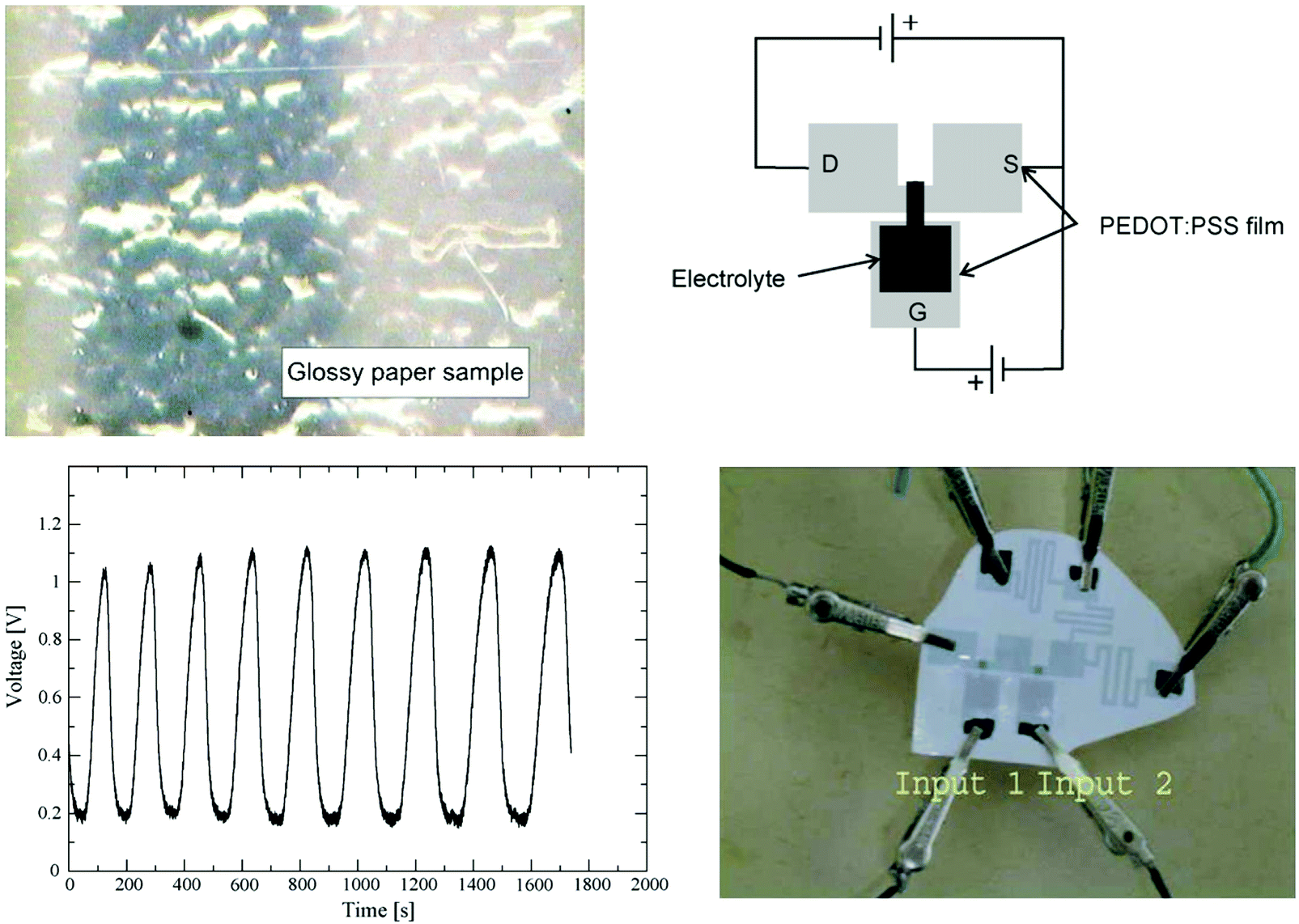 | ||
| Fig. 1 Inkjet-printed organic electrochemical transistors (OECTs) and circuits fabricated by Mannerbro et al. on commercially available glossy photo paper. The transistors were fabricated using inkjet-printed PEDOT:PSS and an inkjet-printed electrolyte. The graph (bottom left) shows the measured output signal of a 5-stage ring oscillator based on resistive-load inverters, indicating a signal propagation delay of 20 s at a supply voltage of 1 V. Reprinted with permission.15 Copyright 2008, Elsevier. | ||
3. Organic field-effect transistors on paper
The first organic field-effect transistors fabricated on paper were reported by Eder et al. in 2004.18 Commercially available hot-pressed cotton-fiber paper was chosen as the substrate, and its surface was sealed prior to the fabrication of the TFTs with a layer of polyvinylphenol (PVP) with a thickness of a few hundred nanometers. On this surface, the TFTs were fabricated in the bottom-gate, bottom-contact architecture using a combination of vacuum deposition (for the gate electrodes, source/drain contacts and semiconductor layer), spin-coating (for the PVP gate dielectric), photolithography, and wet and dry etching. The small-molecule material pentacene was employed as the semiconductor. TFTs with a channel length of 50 μm had a carrier mobility of 0.2 cm2 V−1 s−1 and an on/off current ratio of 106, both notably smaller compared to pentacene TFTs fabricated on plastic substrates. From a 5-stage unipolar ring oscillator based on TFTs with a channel length of 10 μm, a signal propagation delay of 12 ms per stage was obtained at a supply voltage of 50 V, which was inferior by about two orders of magnitude compared to the signal delay measured on similar ring oscillators fabricated on plastics.Also in 2004, Kim et al. described the fabrication of bottom-gate, bottom-contact polymer TFTs on commercially available photo paper, sealed with a stack of vapor-deposited parylene having a thickness of 5 to 20 μm and silicon dioxide deposited by electron-beam evaporation having a thickness of 50 nm.19,20 This double-layer coating was shown to significantly reduce the surface roughness of the paper. The gate dielectric was a combination of a 40 nm-thick layer of polyimide deposited by spin-coating and a 210 nm-thick layer of electron-beam-evaporated SiO2. Regioregular poly(3-hexylthiophene) (P3HT) was used as the semiconductor and deposited either by spin-coating or microcontact-printing. The TFTs had a channel length of 25 μm, a carrier mobility of 0.086 cm2 V−1 s−1 (similar to the highest mobilities reported up to that point for P3HT TFTs), and an on/off current ratio of 104.
Bollström et al.21 developed a multilayer coating system consisting of four different materials deposited successively onto the paper surface: a pre-coating layer of ground calcium carbonate (GCC), a smoothing layer of aluminum silicate hydroxide (kaolin), a barrier layer of acrylic or styrene acrylic copolymer latex blended with precipitated calcium carbonate (to produce a polar surface), and a calendered top-coating layer of kaolin. On this coated paper, the authors fabricated P3HT TFTs in the top-gate architecture using inkjet-printed silver source and drain contacts and polyvinylphenol (PVP) as the gate insulator. The hygroscopic nature of the PVP resulted in a very large gate-insulator capacitance, allowing these TFTs to be operated with voltages of about 1 V. However, due to the significant leakage currents, the TFTs in this initial report had a very small on/off current ratio (about 10). On the same type of paper, Pettersson et al.22 later fabricated P3HT TFTs in which an ion-gel electrolyte obtained by gelation of a triblock copolymer (poly(styrene-block-ethylene oxide-block-styrene); PS–PEO–PS) in an ionic liquid (1-ethyl-3-methylimidazolium bis(trifluoromethylsulfonyl)imide; [EMIM][TFSI])23 was employed as the gate insulator. Owing to the large capacitance of the ion-gel electrolyte, these TFTs also had very low operating voltages (2 V), but a significantly improved on/off current ratio (about 106). On a 3-stage unipolar ring oscillator, the authors measured a signal propagation delay of 35 ms per stage at a supply voltage of 3 V.22
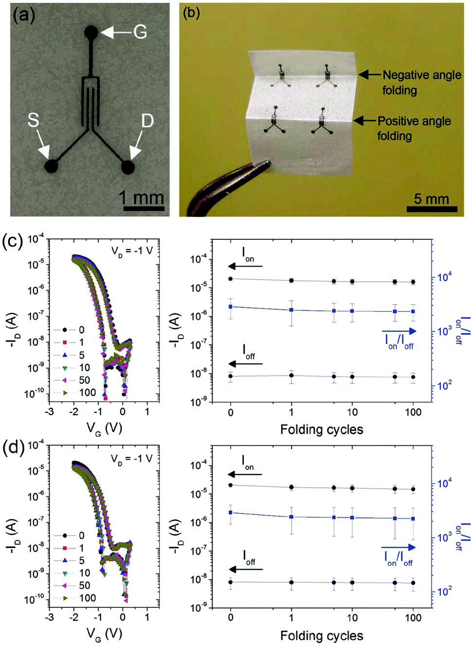
In 2011, we showed that the large surface roughness of paper does not necessarily prevent the use of very thin gate dielectrics in the fabrication of organic TFTs.24 Employing a hybrid gate dielectric consisting of a 3.6 nm-thick layer of oxygen-plasma-grown aluminum oxide (AlOx) and a 2.1 nm-thick self-assembled monolayer (SAM) of an alkylphosphonic acid, we fabricated bottom-gate, top-contact p-channel and n-channel TFTs and unipolar and complementary inverters directly on the surface of four different types of banknotes. The large capacitance of the thin AlOx/SAM gate dielectric allowed these TFTs to operate with gate–source and drain–source voltages of 3 V, similar to the operating voltages of electrochemical and electrolyte-gated transistors, while offering the potential for higher switching frequencies. Except for the phosphonic acid SAM, all materials were grown or deposited in vacuum, and all patterning was performed using shadow masks and thus without the need for photoresists and subtractive patterning. The TFTs had channel lengths ranging from 10 to 30 μm. The p-channel TFTs were fabricated using the small-molecule semiconductor dinaphtho[2,3-b:2′,3′-f]thieno[3,2-b]thiophene (DNTT) and had a carrier mobility of 0.57 cm2 V−1 s−1, an on/off current ratio of 105 and a subthreshold slope of 0.11 V per decade. Hexadecafluorocopperphthalocyanine (F16CuPc) was used for the n-channel TFTs, providing an electron mobility of 0.005 cm2 V−1 s−1, an on/off current ratio of 104 and a subthreshold slope of 0.26 V per decade. Unipolar inverters showed switching frequencies of about 2 kHz.
The fabrication of electronic devices on banknotes is partially motivated by the possibility of implementing active security and anti-counterfeiting features directly on the surface of the banknotes. In addition to TFTs and digital circuits, this would likely also require some type of memory devices. In 2012, Khan et al. reported on the fabrication of ferroelectric memory TFTs on a banknote.25 The bottom-gate, top-contact TFTs were fabricated using polydimethylsiloxane (PDMS) as a planarization layer, PEDOT:PSS for the gate electrodes, the ferroelectric copolymer poly(vinylidene fluoride–trifluoroethylene) (P(VDF–TrFE)) as the gate dielectric (all deposited by spin-coating), and vacuum-deposited pentacene as the semiconductor. The TFTs had a channel length of 60 μm, a carrier mobility of 0.12 cm2 V−1 s−1, an on/off current ratio of 103, a memory window of about 8 V, and a retention time of several hours.
The first organic transistors on paper that showed a carrier mobility greater than 1 cm2 V−1 s−1 were reported in 2012 by Li et al.26 Perhaps more important than the large carrier mobility was the fact that these TFTs also had a very large on/off current ratio of 108. The bottom-gate, top-contact TFTs were fabricated on commercially available photo paper coated with a 3 μm-thick layer of vapor-polymerized parylene. A 500 nm-thick gate dielectric of the fluoropolymer Cytop and a blend of the small-molecule semiconductor 2,7-dioctyl[1]benzothieno[3,2-b][1]benzothiophene (C8-BTBT) and the insulating polymer poly(methyl methacrylate) (PMMA) were successively deposited by spin-coating. The large carrier mobility was in part due to the formation of large crystalline domains in the semiconductor layer resulting from the phase separation in the solution-deposited C8-BTBT/PMMA blend.
Zhang et al. fabricated organic TFTs and circuits on a 320 nm-thick stack of polyacrylonitrile (PAN) and polystyrene (PS) that served as both the substrate and the gate dielectric, and this plastic sheet with the TFTs and circuits was then laminated onto the surface of a banknote.27 The p-channel pentacene and n-channel bis(octyl)-perylene tetracarboxylic diimide (PTCDI-(C8H17)2) TFTs had hole and electron mobilities of 0.52 cm2 V−1 s−1 and 0.23 cm2 V−1 s−1, respectively. A 5-stage complementary ring oscillator showed a signal propagation delay of 59 μs per stage at a supply voltage of 50 V.
Peng et al. screen-printed silver-nanoparticle-based gate electrodes directly onto the surface of commercially available laser-printing paper to fabricate bottom-gate, top-contact TFTs with a vapor-deposited parylene gate dielectric (680 nm or 2 μm thick), vacuum-deposited DNTT as the semiconductor, and screen-printed silver-nanoparticle-based source and drain contacts.28,29 With a channel length of 85 μm, these TFTs showed carrier mobilities between about 0.3 and 0.6 cm2 V−1 s−1, on/off current ratios up to 108, a subthreshold slope of 0.9 V per decade and a transit frequency of 50 kHz, quite similar to the performance of TFTs fabricated on a plastic substrate and with excellent uniformity across an array of 64 TFTs (see Fig. 2).
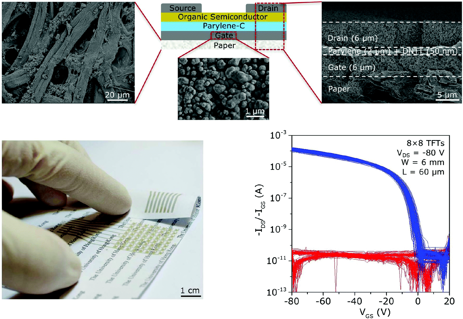 | ||
| Fig. 2 Array of organic TFTs fabricated by Peng et al. on commercially available laser-printing paper using screen-printed silver-nanoparticle-based gate electrodes and source/drain contacts, a 2 μm-thick vapor-deposited parylene gate dielectric and vacuum-deposited DNTT as the semiconductor. The TFTs have an average carrier mobility of 0.45 cm2 V−1 s−1, and average on/off current ratio of 108, a subthreshold slope of 0.9 V per decade and a transit frequency of 50 kHz. Reprinted with permission.29 Copyright 2014, Nature Publishing Group. | ||
Zocco et al. compared the performance of pentacene TFTs fabricated on glass and on two types of commercially available paper, Hewlett Packard photo paper and Sappi High Gloss specialty paper.30 320 nm-thick parylene was used as the gate dielectric. The TFT performance turned out to be very similar on all three substrates, with carrier mobilities of 0.11, 0.09 and 0.05 cm2 V−1 s−1 on the glass, the photo paper and the specialty paper, respectively. These results again show that parylene can be a very suitable surface-coating and gate-dielectric material for the fabrication of high-performance organic TFTs on paper.
The largest carrier mobility published to date for organic transistors on paper is 2.5 cm2 V−1 s−1, and these TFTs were reported by Minari et al. in 2014.31 On commercially available photo (inkjet) paper coated with a 3 μm-thick layer of parylene, the authors fabricated top-gate TFTs based on the small-molecule semiconductor C8-BTBT. The semiconductor layer was deposited by drop-casting and formed a polycrystalline layer consisting of large crystalline domains. Gold nanoparticles functionalized with conjugated molecular ligands and patterned using a combination of photolithography and solution-coating were employed to form the source and drain contacts and the gate electrodes, with a stack of two fluoropolymers with a total thickness of 500 nm serving as the gate dielectric. The TFTs had a channel length of 100 μm, and in addition to a record mobility of 2.5 cm2 V−1 s−1, they showed an on/off current ratio of 106 and a subthreshold slope of 1.4 V per decade (see Fig. 3).
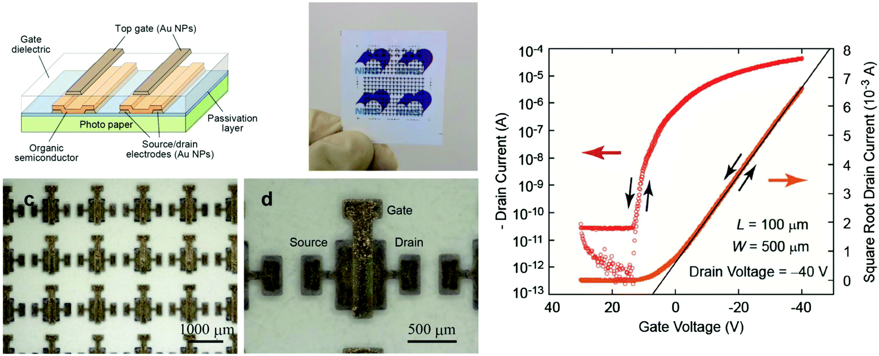 | ||
| Fig. 3 Organic TFTs fabricated by Minari et al. on commercially available photo paper showing a carrier mobility of 2.5 cm2 V−1 s−1, the largest carrier mobility reported to date for organic transistors on paper. Prior to TFT fabrication, the paper was coated with a 3 μm-thick layer of parylene. Gold nanoparticles functionalized with conjugated molecular ligands and patterned using a combination of photolithography and solution-coating were employed to form the source and drain contacts and the gate electrodes. Reprinted with permission.31 Copyright 2014, Wiley-VCH. | ||
Rather than sealing the entire paper surface with a blanket smoothing layer prior to transistor fabrication, Grau et al. employed gravure printing to apply a surface coating only in those regions in which the TFTs were to be fabricated, thus preserving the natural properties of the paper in the remaining areas.32 Gravure printing is an established, mass-production-capable, high-quality, multi-purpose roll-to-roll printing technique and was utilized here to locally coat the paper with 6 μm-thick polyvinylphenol (PVP) and to print the 200 nm-thick PVP gate dielectric of the bottom-gate, bottom-contact polymer TFTs. Inkjet printing was used to define Ag-nanoparticle-based gate electrodes and source/drain contacts. The semiconducting polymer poly(2,5-bis(3-tetradecyl-thiophen-2-yl)thieno[3,2-b]thiophene) (pBTTT) was deposited by spin-coating. The TFTs had a channel length of 25 μm, a carrier mobility of 0.086 cm2 V−1 s−1, an on/off current ratio above 104 and a subthreshold slope of 18 V per decade.
4. Organic transistors on nanocellulose, supercalendered and specialty paper
When paper is manufactured by traditional papermaking techniques, the microstructure of the cellulose fibers is mostly preserved. Depending on the type of wood from which the cellulose is obtained, these fibers have a diameter of 10 to 20 μm, which is the main reason for the large surface roughness of regular paper. An alternative approach to papermaking is to first disintegrate the cellulose fibers by high-pressure homogenization into their constituent fibrils, called micro- or nanofibrillated cellulose (MFC, NFC), cellulose nanofibers (CNF), cellulose nanocrystals (CNC) or nanocellulose. These can then be pressed into thin sheets to produce cellulose nanopaper.33 Due to the small diameter of the nanofibers or nanocrystals (between a few nanometers to a few tens of nanometers), nanopaper is significantly smoother than regular paper. Organic TFTs fabricated on nanopaper were reported by Chinga-Carrasco et al. in 2012, by Huang et al. in 2013, by Fujisaki et al. in 2014, by Wang et al. in 2015, and by Dai et al. in 2018.34–38Chinga-Carrasco et al.34 explored the effect of treating the cellulose nanofibers prior to homogenization by carboxymethylation or 2,2,6,6-tetramethylpiperidine-1-oxyl-mediated oxidation and modified the nanopaper surface with a hexamethyldisilazane coating. On this surface, the authors fabricated top-gate p-channel polymer TFTs based on inkjet-printed silver-nanoparticle source/drain contacts, spin-coated poly(3,3′′-didodecyl-quaterthiophene) (PQT-12) and PVP as semiconductor and gate insulator, and drop-cast PEDOT:PSS gate electrodes. Due to the hygroscopic nature of the PVP, these TFTs had very low operating voltages (2 V), but also a very small on/off current ratio, similar to the TFTs reported earlier by Bollström et al.21
Huang et al.35 applied a hot-pressing process to produce nanopaper sheets with a preferred thickness. On these sheets, the authors fabricated bottom-gate, top-contact n-channel TFTs using a 1 μm-thick PMMA gate dielectric deposited by spin-coating and a vacuum-deposited layer of the small-molecule semiconductor bis(pentadecafluorooctyl)-naphthalene tetracarboxylic diimide (NTCDI-(CH2C7F15)2). These TFTs had a channel length of 100 μm, an electron mobility of 0.004 cm2 V−1 s−1 and an on/off current ratio of 200 (the latter possibly limited by lack of patterning of the semiconductor layer).
Fujisaki et al.36 took advantage of a modified protocol that preserved the native chemical structure of the cellulose in the nanofibers, yielding nanopaper with greatly improved thermal stability. The authors coated their 20 μm-thick nanopaper with a 2 μm-thick olefin polymer and fabricated bottom-gate, bottom-contact p-channel polymer TFTs with a channel length of 10 μm using a 300 nm-thick fluoropolymer gate dielectric; these TFTs had a carrier mobility of 1.3 cm2 V−1 s−1, on/off current ratios up to 108 and a subthreshold slope of 0.84 V per decade (see Fig. 4).
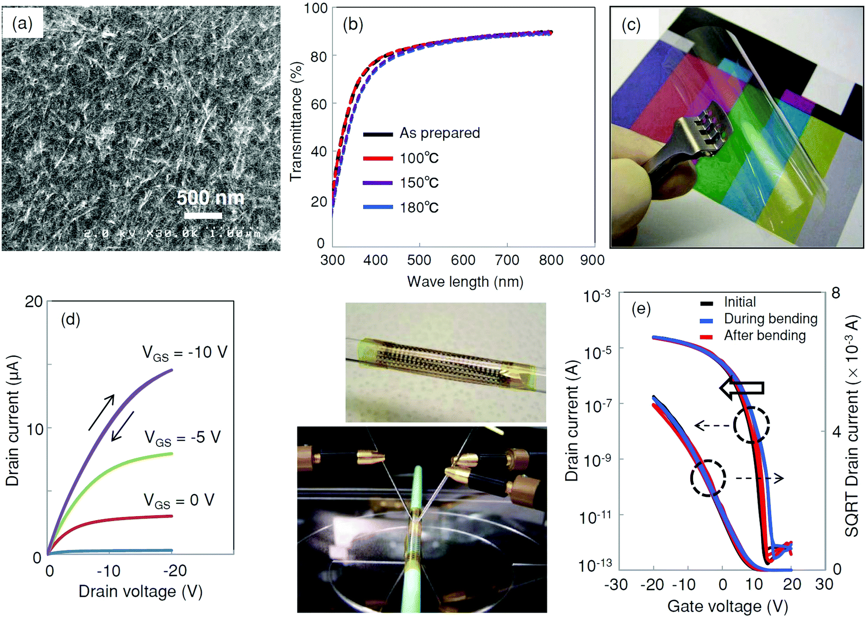 | ||
| Fig. 4 Polymer TFTs fabricated by Fujisaki et al. on optically transparent heat-resistant nanocellulose paper (nanopaper). The TFTs have a channel length of 10 μm and excellent electrical performance, including a carrier mobility of 1.3 cm2 V−1 s−1, an on/off ratio of 108 and a subthreshold slope of 0.84 V per decade. Reprinted with permission.36 Copyright 2014, Wiley-VCH. | ||
Instead of nanofibers, Wang et al.37 utilized nanocrystals, which tend to be shorter than nanofibers (tens or hundreds of nanometers, rather than several microns) and thus tend to give a smoother surface of the nanopaper produced from them. Atomic layer deposition (ALD) was then used to coat the nanopaper with a thin aluminum-oxide layer, on which the authors fabricated top-gate TFTs based on a phase-separating blend of TIPS pentacene and poly[bis(4-phenyl)(2,4,6-trimethylphenyl)amine] (PTAA). The gate dielectric was a stack of 35 nm-thick Cytop (deposited by spin-coating) and 40 nm-thick Al2O3 (deposited by ALD). Owing to the relatively small thickness and large capacitance (31 nF cm−2) of this double-layer gate dielectric, it was possible to operate these TFTs with relatively low voltages of 10 V. The TFTs had a channel length of 180 μm, a carrier mobility of 0.23 cm2 V−1 s−1, an on/off ratio of 104 and a subthreshold slope of 0.9 V per decade.
Dai et al.38 exploited the fact that the 2,2,6,6-tetramethylpiperidine-1-oxyl-mediated oxidation process introduces a significant density of mobile sodium ions into the nanocellulose, which makes the nanopaper also an electrolyte. To fabricate TFTs, the authors used a sheet of 40 μm-thick nanopaper with a capacitance of 220 nF cm−2 as both the substrate and the gate insulator, with the gate electrodes located on one surface and the organic semiconductor and the source/drain contacts located on the other surface of the substrate. Both p-channel and n-channel TFTs were fabricated, using C8-BTBT, PQT-12 and NTCDI-(CH2C7F15)2 as the semiconductors. The TFTs had a channel length of 100 μm, carrier mobilities between 0.01 and 0.07 cm2 V−1 s−1, and on/off current ratios of about 103.
One drawback of manufacturing nanocellulose is that the process of disintegrating the native cellulose fibers into nanocellulose is associated with a relatively large energy consumption. An alternative is supercalendering, a technique in which conventionally manufactured paper is flattened at the end of the papermaking process by passing it through stacks of hard and soft cylindrical rollers. Paper produced by supercalendering is called glassine and is often used as an interleaving paper to protect fine art or delicate objects from contact with other materials. Its smooth surface makes glassine also useful for flexible electronics. In 2015, Hyun et al. reported on the fabrication of electrolyte-gated polymer TFTs on glassine paper in a side-gate architecture, using screen-printed graphene to define the gate electrodes and the source and drain contacts on the substrate surface, aerosol-jet-printed poly(3-hexylthiophene) P3HT as the semiconductor, and a drop-cast ion-gel electrolyte.39 Due to the large capacitance of the electrolyte (22 μF cm−2), the TFTs had a low operating voltage of 2 V. For TFTs with a channel length of 60 μm, the authors demonstrated a carrier mobility of 0.14 cm2 V−1 s−1, an on/off ratio of about 103, and excellent bending stability of the TFTs (see Fig. 5).
 | ||
| Fig. 5 Electrolyte-gated organic TFTs fabricated by Hyun et al. on glassine paper in a side-gate architecture using screen-printed graphene source/drain contacts and gate electrodes, aerosol-jet-printed poly(3-hexylthiophene) and a drop-cast ion-gel electrolyte. The TFTs have a carrier mobility of 0.14 cm2 V−1 s−1, an on/off ratio of about 103 and excellent bending stability. Reprinted with permission.39 Copyright 2015, Wiley-VCH. | ||
In response to the specific demands of flexible and printed electronics in terms of the substrate properties, a number of paper manufacturers have developed and commercialized specialty paper characterized by a small surface roughness. One example is PowerCoat™ HD from Arjowiggins Creative Papers, which was introduced in 2014. On this substrate, Wang et al.40 and later Raghuwanshi et al.41 fabricated organic TFTs based on a phase-separating blend of TIPS pentacene and either PTAA or polystyrene. The gate dielectric was a stack of an insulating polymer (either 45 nm-thick Cytop or 160 nm-thick PVP, deposited by spin-coating) and an insulating metal oxide (40 nm-thick Al2O3 and/or HfO2, deposited by atomic layer deposition). The TFTs had a channel length of 90 or 180 μm, operating voltages of 10 V, a carrier mobility of about 0.4 cm2 V−1 s−1 and an on/off ratio of 105, and they displayed excellent long-term stability. Another brand of smooth specialty paper for printed electronics is p_e:smart from the Felix Schoeller Group, also introduced around 2014. On this paper, Mitra et al. fabricated top-gate polymer TFTs in which all functional layers were deposited by inkjet printing.42 Two different commercially available silver-nanoparticle inks were printed to define the source/drain contacts and the gate electrodes, an epoxy/nanosilica ink was used for the 4 μm-thick gate dielectric, and the amorphous polymer poly[bis(4-phenyl)(2,4,6-trimethylphenyl)amine] was employed as the semiconductor. The TFTs had a channel length of 50 μm, a carrier mobility of 0.087 cm2 V−1 s−1 and an on/off ratio of 102 (see Fig. 6).
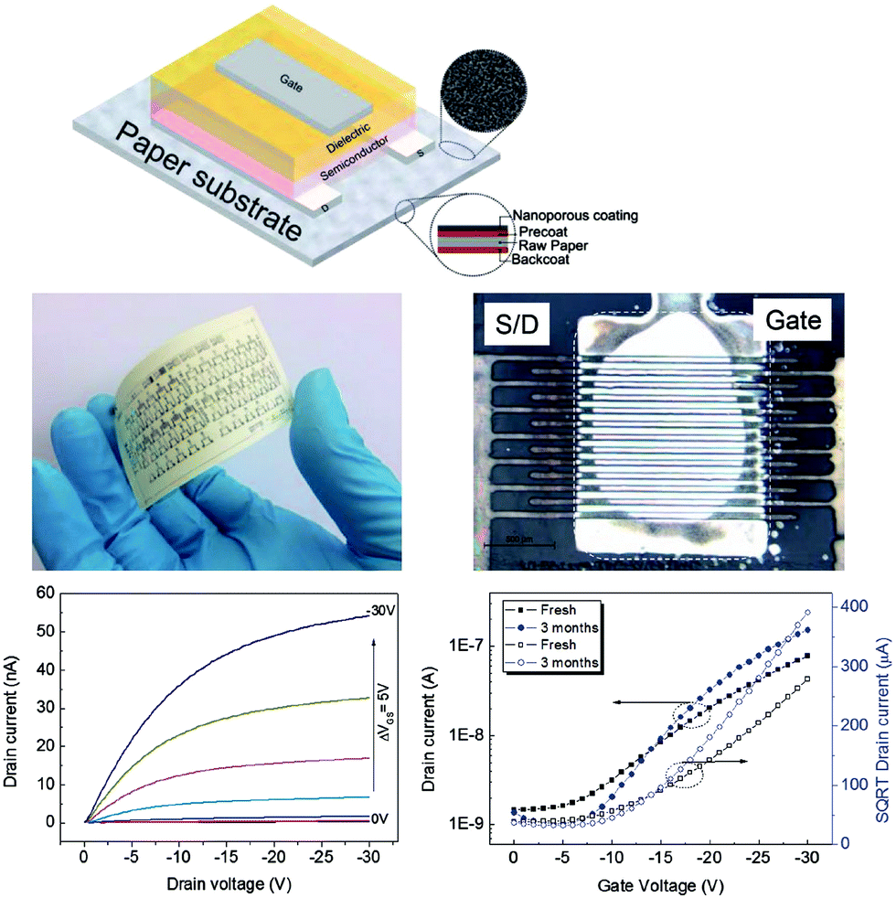 | ||
| Fig. 6 Fully inkjet-printed polymer TFTs fabricated by Mitra et al. on commercially available specialty paper (p_e:smart; Felix Schoeller Group). All TFT layers (source/drain contacts, semiconductor, gate dielectric, gate electrodes) were deposited by inkjet printing. Reprinted with permission.42 Copyright 2017, Wiley-VCH. | ||
For certain applications, such as conformable sensor arrays, a substrate with a thickness of less than 1 μm may be required. Lei et al. thus prepared sheets of paper with a thickness of 800 nm and a size of a few square-centimeters by reacting microcrystalline cellulose with hexamethyldisilazane, depositing the product onto a solid substrate by spin-coating and hydrolyzing the film in acetic acid vapor.43 On the 800 nm-thick substrates, the authors fabricated bottom-gate, top-contact TFTs based on a decomposable (natural-dye-based) semiconducting polymer with a channel length of 50 μm, a carrier mobility of 0.21 cm2 V−1 s−1 and an on/off current ratio of 105.
Paper is usually manufactured from cellulose, a linear polysaccharide forming the main structural component of the cell walls of green plants, including wood and cotton. A potential alternative to cellulose for papermaking is starch, which consists of linear and branched polysaccharides and is contained in large quantities in various agricultural crops, such as rice, wheat, corn and potatoes. In 2018, Jeong et al. reported on the preparation of thin, smooth and optically transparent substrates by gelatinization of potato starch (blended with a small amount of chemically crosslinked polyvinyl alcohol to enhance the mechanical properties) and on the fabrication of bottom-gate, top-contact TFTs on these substrates.44 The authors used a vapor-deposited parylene layer with a thickness of 870 nm as the gate dielectric and evaluated three organic semiconductors: pentacene, DNTT and poly(dimethyl-triarylamine) (PTAA). The best performance was obtained using pentacene and DNTT, for which a carrier mobility of about 0.3 cm2 V−1 s−1 and an on/off current ratio above 105 were obtained.
Lee et al.45 recently described the fabrication of bottom-gate, top-contact pentacene TFTs on Bristol board, a smooth and relatively thick type of paperboard manufactured primarily for applications in fine arts and print media. The TFTs were fabricated directly on the surface of the 2.5 mm-thick paperboard without a coating layer. The TFTs had a channel length of 150 μm, an on/off current ratio of 103 and a subthreshold slope of 0.3 V per decade. As the gate insulator, the authors employed a 630 nm-thick stack of gelatin and gelatin mixed with iron. Due to the electrolytic and hygroscopic properties of gelatin, its permittivity varies over several orders of magnitude depending on the humidity and the frequency at which the measurements are performed, which makes it difficult to extract a meaningful value for the carrier mobility of the TFTs from their current–voltage characteristics. (The authors measured the gate-insulator capacitance at a frequency of 1 MHz and then used the capacitance determined from this measurement to calculate a carrier mobility of 8 cm2 V−1 s−1 for the TFTs, but since the current–voltage characteristics of the TFTs were measured under quasi-static conditions, this value significantly overestimates the true carrier mobility.)
5. Low-voltage organic TFTs and circuits on paper
Finally, we would like to briefly address the issue of low-voltage operation of organic TFTs and circuits fabricated on paper. Given that organic transistors are being developed primarily for mobile systems that will likely be powered by small batteries or solar cells, the maximum available supply voltage will be on the order of a few volts. One possibility to address this issue is the use of a thin, high-capacitance gate dielectric that allows the transistors to operate with small gate–source voltages. For this purpose, we have developed a hybrid AlOx/SAM gate dielectric with a thickness of about 5 nm and a capacitance of about 600 nF cm−2 that allows a charge-carrier density close to 1013 cm−2 to be induced in the organic semiconductor layer at gate–source voltages of about 2 to 3 V.24,46Fig. 7 shows photographs and measured electrical characteristics of p-channel and n-channel organic TFTs and circuits fabricated on commercially available cleanroom paper and on a banknote using this approach. The TFTs and circuits operate with supply voltages between 2 and 4 V, with small static power consumption (<100 pW per stage) and with signal propagation delays of a few microseconds per stage in 11-stage complementary ring oscillators.47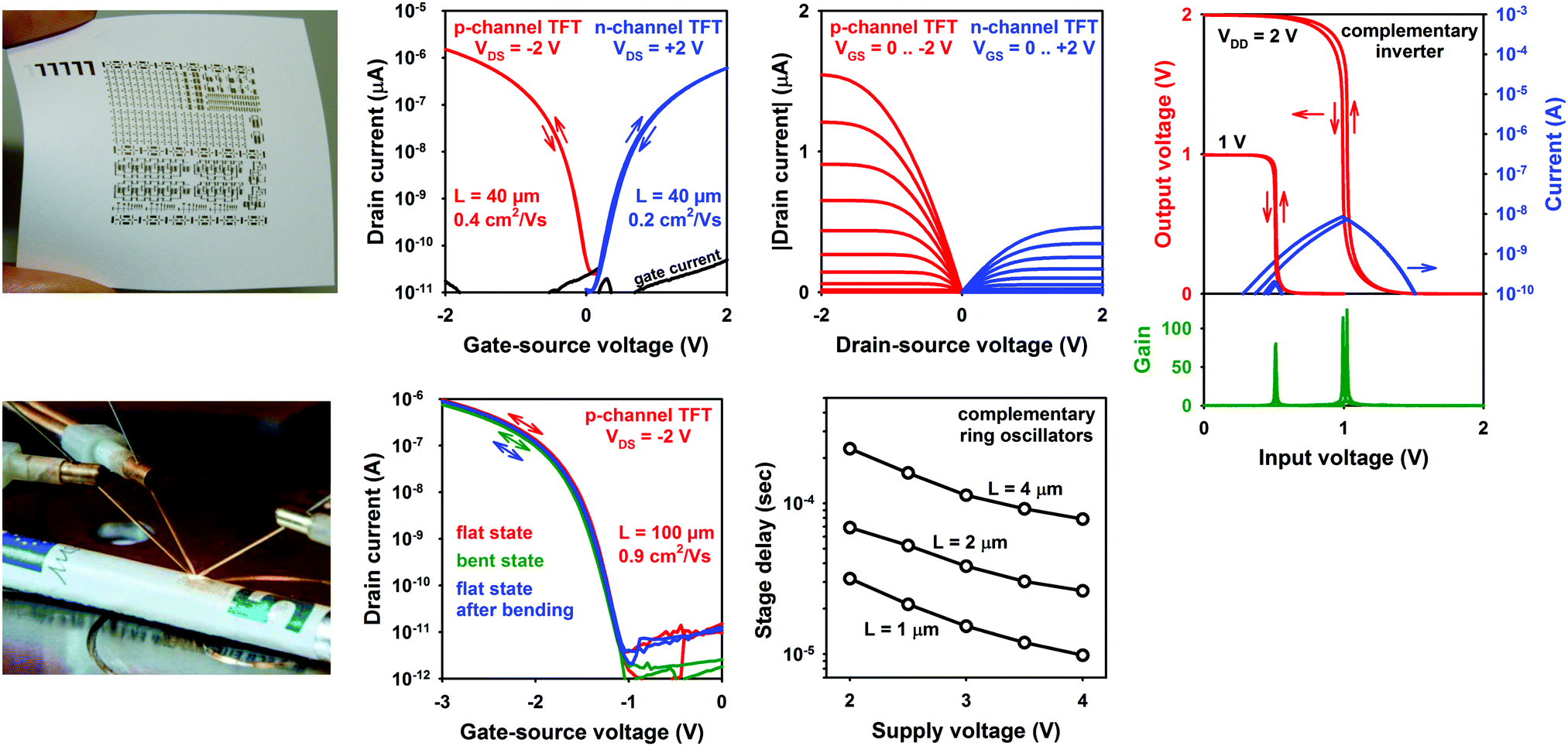 | ||
| Fig. 7 Low-voltage organic TFTs and complementary circuits fabricated on commercially available cleanroom paper (top) and on a banknote (bottom).46,47 | ||
6. Summary and outlook
Table 1 provides a summary of the characteristic properties and performance parameters reported in the literature for organic transistors fabricated on paper. By comparing the device-performance parameters listed in Table 1 with those commonly reported for organic transistors fabricated on plastic substrates, it can be seen that the performance of organic transistors on paper still lags behind that of the best organic transistors on plastic substrates. For example, while hole and electron mobilities of about 5 and 1 cm2 V−1 s−1 are routinely achieved for p-channel and n-channel organic transistors fabricated on plastic substrates, respectively, the mobilities are currently smaller by a factor of about 2 to 5 for organic transistors fabricated on paper. For organic transistors fabricated on plastic substrates, on/off current ratios, subthreshold slopes and signal propagation delays of 109, 62 mV per decade and 138 ns have been reported,48 while the best values for organic transistors on paper are currently 108, 90 mV per decade and 2 μs.26,29,36,46,47 But the same comparison also suggests that the rate at which the performance of organic transistors on paper has been improved over the years is comparable to the rate at which the performance of organic transistors on plastic substrates has been improved. It is therefore not unreasonable to anticipate that paper may eventually replace plastics at least in some applications as the preferred substrate for organic electronics.| Ref. | Type of substrate | Surface coating | Type of devices | Organic semiconductor | Carrier type | Operating voltage (V) | Carrier mobility (cm2 V−1 s−1) | On/off current ratio | Subthr. slope (V dec−1) | Signal delay (s) |
|---|---|---|---|---|---|---|---|---|---|---|
| 14 | Photo paper | PE | OECT | PEDOT:PSS | p | 2 | 105 | |||
| 15 | Photo paper | OECT, RO | PEDOT:PSS | p | 2 | 4 × 101 | 20 | |||
| 17 | Specialty paper | OECT | PEDOT:PSS | p | 0.7 | 3 | ||||
| 18 | Cotton paper | PVP | FET, RO | Pentacene | p | 30 | 0.2 | 106 | 1.8 | 0.012 |
| 19 and 20 | Photo paper | Parylene/SiO2 | FET | Poly(3-hexylthiophene) | p | 40 | 0.086 | 104 | ||
| 21 | Fine paper | 4-Layer | EGFET | Poly(3-hexylthiophene) | p | 1 | 101 | |||
| 22 | Fine paper | 4-Layer | EGFET, RO | P3HT/PLLA | p | 2 | 106 | 0.035 | ||
| 24 | Banknotes | FET, inv. | DNTT | p | 3 | 0.57 | 105 | 0.11 | ||
| 24 | Banknotes | FET, inv. | F16CuPc | n | 3 | 0.005 | 104 | 0.26 | ||
| 25 | Banknotes | PDMS | FeFET | Pentacene | p | 15 | 0.12 | 103 | ||
| 26 | Photo paper | Parylene | FET | C8-BTBT | p | 40 | 1.3 | 108 | 2.0 | |
| 27 | Banknotes | FET, RO | Pentacene | p | 15 | 0.52 | 105 | 5.9 × 10⁻⁵ | ||
| 27 | Banknotes | FET, RO | PTCDI-(C8H17)2 | n | 15 | 0.23 | 107 | |||
| 28 | Printer paper | FET | DNTT | p | 30 | 0.39 | 2 × 10⁶ | 0.9 | ||
| 29 | Printer paper | FET | DNTT | p | 80 | 0.56 | 108 | 1.4 | ||
| 30 | Photo paper | FET | Pentacene | p | 60 | 0.09 | 105 | |||
| 31 | Photo paper | Parylene | FET | C8-BTBT | p | 40 | 2.5 | 106 | 1.4 | |
| 32 | Packing paper | Kaolin/PVP | FET | pBTTT | p | 40 | 0.086 | 3 × 10⁴ | 18 | |
| 34 | Nanopaper | HMDS | EGFET | PQT-12 | p | 2 | 14 | |||
| 35 | Nanopaper | FET | NTCDI-(CH2C7F15)2 | n | 80 | 0.0043 | 2 × 10² | |||
| 36 | Nanopaper | Olefin polymer | FET | Merck Lisicon S1200 | p | 20 | 1.3 | 108 | 0.84 | |
| 37 | Nanopaper | Al2O3 | FET | TIPS pentacene/PTAA | p | 10 | 0.23 | 104 | 0.9 | |
| 38 | Nanopaper | EGFET | C8-BTBT | p | 10 | 0.072 | 7 × 10³ | |||
| 38 | Nanopaper | EGFET | PQT-12 | p | 10 | 0.021 | 3 × 10² | |||
| 38 | Nanopaper | EGFET | NTCDI-(CH2C7F15)2 | n | 10 | 0.01 | 2 × 10³ | |||
| 39 | Glassine | EGFET | Poly(3-hexylthiophene) | p | 2 | 0.14 | 5 × 10³ | |||
| 40 | PowerCoat HD | PVA/PVP | FET | TIPS pentacene/PTAA | p | 10 | 0.39 | 4 × 10⁵ | 0.9 | |
| 41 | PowerCoat HD | PVA | FET | TIPS pentacene/PS | p | 10 | 0.44 | 105 | ||
| 42 | p_e:smart | FET | PTAA | p | 30 | 0.087 | 102 | |||
| 43 | Thin paper | FET | PDPP-PD | p | 10 | 0.21 | 105 | |||
| 44 | Starch paper | FET | Pentacene | p | 40 | 0.37 | 5 × 10⁵ | |||
| 44 | Starch paper | FET | DNTT | p | 40 | 0.36 | 105 | |||
| 44 | Starch paper | FET | PTAA | p | 40 | 0.013 | 7 × 10⁴ | |||
| 45 | Bristol board | EGFET | Pentacene | p | 5 | 103 | 0.3 | |||
| 46 | Cleanroom paper | FET | DNTT | p | 2 | 1.6 | 106 | 0.09 | ||
| 47 | Banknotes | FET, RO | DNTT | p | 3 | 1.12 | 107 | 0.1 | 2 × 10⁻⁶ | |
| 47 | Banknotes | FET, RO | ActivInk™ N1100 | n | 3 | 0.15 | 4 × 10⁶ | 0.17 |
One aspect for future work will be the further reduction of the operating voltage of the transistors, because operating voltages greater than about 10 V are unrealistic for most applications. There are more than a hundred publications in which operating voltages of 1 V or less have been reported for organic transistors fabricated on glass, silicon or plastic substrates,49 while for organic transistors on paper, only one such report exists.17 This may reflect the difficulty of minimizing the gate-dielectric thickness without introducing prohibitively large gate leakage on substrates with significant surface roughness, but this must be considered a solvable problem. Another interesting challenge will be the fabrication of organic permeable-base transistors50 on paper. Organic permeable-base transistors are usually fabricated in a vertical architecture, which means that tight control of the thicknesses of the various layer in the transistors is even more critical than in planar field-effect transistors, and this will certainly lead to some interesting issues. Finally, a variety of aspects related to the integration of organic transistors into circuits and systems will need to be addressed, including device-parameter uniformity, passive components (capacitors, resistors), robust circuit design, signal integrity, memory, reliability and packaging.51,52
Conflicts of interest
There are no conflicts to declare.Acknowledgements
Open Access funding provided by the Max Planck Society.References
- Z. A. Lamport, H. F. Haneef, S. Anand, M. Waldrip and O. D. Jurchescu, Tutorial: organic field-effect transistors: materials, structure and operation, J. Appl. Phys., 2018, 124, 071101 CrossRef.
- C. Wang, H. Dong, W. Hu, Y. Liu and D. Zhu, Semiconducting π-Conjugated Systems in Field-Effect Transistors: A Material Odyssey of Organic Electronics, Chem. Rev., 2012, 112, 2208 CrossRef CAS PubMed.
- H. Sirringhaus, Organic field-effect transistors: the path beyond amorphous silicon, Adv. Mater., 2014, 26, 1319 CrossRef CAS PubMed.
- X. Guo, Y. Xu, S. Ogier, T. N. Ng, M. Caironi, A. Perinot, L. Li, J. Zhao, W. Tang, R. A. Sporea, A. Nejim, J. Carrabina, P. Cain and F. Yan, Current Status and Opportunities of Organic Thin-Film Transistor Technologies, IEEE Trans. Electron Devices, 2017, 64, 1906 CAS.
- H. Li, W. Shi, J. Song, H.-J. Jang, J. Dailey, J. Yu and H. E. Katz, Chemical and Biomolecule Sensing with Organic Field-Effect Transistors, Chem. Rev., 2019, 119, 3 CrossRef CAS PubMed.
- J. Rivnay, S. Inal, A. Salleo, R. M. Owens, M. Berggren and G. G. Malliaras, Organic electrochemical transistors, Nat. Rev. Mater., 2018, 3, 17086 CrossRef CAS.
- M. Irimia-Vladu, N. S. Sariciftci and S. Bauer, Exotic materials for bio-organic electronics, J. Mater. Chem., 2011, 21, 1350 RSC.
- M. Irimia-Vladu, E. D. Głowacki, G. Voss, S. Bauer and N. S. Sariciftci, Green and biodegradable electronics, Mater. Today, 2012, 15, 340 CrossRef CAS.
- M. Irimia-Vladu, Green electronics: biodegradable and biocompatible materials and devices for sustainable future, Chem. Soc. Rev., 2014, 43, 588 RSC.
- Green Materials for Electronics, ed. M. Irimia-Vladu, E. D. Głowacki, N. S. Sariciftci and S. Bauer, Wiley-VCH, 2017, ISBN: 978-3-527-33865-8 Search PubMed.
- D. Tobjörk and R. Österbacka, Paper Electronics, Adv. Mater., 2011, 23, 1935 CrossRef PubMed.
- Y. Lin, D. Gritsenko, Q. Liu, X. Lu and J. Xu, Recent Advancements in Functionalized Paper-Based Electronics, ACS Appl. Mater. Interfaces, 2016, 8, 20501 CrossRef CAS PubMed.
- D. Ha, Z. Fang and N. B. Zhitenev, Paper in Electronic and Optoelectronic Devices, Adv. Electron. Mater., 2018, 4, 1700593 CrossRef.
- P. Andersson, D. Nilsson, P.-O. Svensson, M. Chen, A. Malmström, T. Remonen, T. Kugler and M. Berggren, Active Matrix Displays Based on All-Organic Electrochemical Smart Pixels Printed on Paper, Adv. Mater., 2002, 14, 1460 CrossRef CAS.
- R. Mannerbro, M. Ranlöf, N. Robinson and R. Forchheimer, Inkjet printed electrochemical organic electronics, Synth. Met., 2008, 158, 556 CrossRef CAS.
- D. Khodagholy, J. Rivnay, M. Sessolo, M. Gurfinkel, P. Leleux, L. H. Jimison, E. Stavrinidou, T. Herve, S. Sanaur, R. M. Owens and G. G. Malliaras, High transconductance organic electrochemical transistors, Nat. Commun., 2013, 4, 2133 CrossRef PubMed.
- E. Bihar, Y. Deng, T. Miyake, M. Saadaoui, G. G. Malliaras and M. Rolandi, A Disposable paper breathalyzer with an alcohol sensing organic electrochemical transistor, Sci. Rep., 2016, 6, 27582 CrossRef CAS PubMed.
- F. Eder, H. Klauk, M. Halik, U. Zschieschang, G. Schmid and C. Dehm, Organic electronics on paper, Appl. Phys. Lett., 2004, 84, 2673 CrossRef CAS.
- Y.-H. Kim, D.-G. Moon and J.-I. Han, Organic TFT Array on a Paper Substrate, IEEE Electron Device Lett., 2004, 25, 702 CrossRef CAS.
- Y. H. Kim, D. G. Moon, W. K. Kim and J. I. Han, Organic thin-film devices on paper substrates, J. Soc. Inf. Disp., 2005, 13, 829 CrossRef CAS.
- R. Bollström, A. Määttänen, D. Tobjörk, P. Ihalainen, N. Kaihovirta, R. Österbacka, J. Peltonen and M. Toivakka, A multilayer coated fiber-based substrate suitable for printed functionality, Org. Electron., 2009, 10, 1020 CrossRef.
- F. Pettersson, R. Österbacka, J. Koskela, A. Kilpelä, T. Remonen, Y. Zhang, S. Inkinen, C.-E. Wilen, R. Bollström, M. Toivakka, A. Määttänen, P. Ihalainen and J. Peltonen, Ion-modulated transistors on paper using phase-separated semiconductor/insulator blends, MRS Commun., 2014, 4, 51 CrossRef CAS.
- J. H. Cho, J. Lee, Y. He, B. Kim, T. P. Lodge and C. D. Frisbie, High-capacitance ion gel gate dielectrics with faster polarization response times for organic thin film transistors, Adv. Mater., 2008, 20, 686 CrossRef CAS.
- U. Zschieschang, T. Yamamoto, K. Takimiya, H. Kuwabara, M. Ikeda, T. Sekitani, T. Someya and H. Klauk, Organic electronics on banknotes, Adv. Mater., 2011, 23, 654 CrossRef CAS PubMed.
- M. A. Khan, U. S. Bhansali and H. N. Alshareef, High-performance non-volatile organic ferroelectric memory on banknotes, Adv. Mater., 2012, 24, 2165 CrossRef CAS PubMed.
- Y. Li, C. Liu, Y. Xu, T. Minari, P. Darmawan and K. Tsukagoshi, Solution-processed organic crystals for field-effect transistor arrays with smooth semiconductor/dielectric interface on paper substrates, Org. Electron., 2012, 13, 815 CrossRef CAS.
- L. Zhang, H. Wang, Y. Zhao, Y. Guo, W. Hu, G. Yu and Y. Liu, Substrate-free ultra-flexible organic field-effect transistors and five-stage ring oscillators, Adv. Mater., 2013, 25, 5455 CrossRef CAS PubMed.
- B. Peng and P. K. L. Chan, Flexible organic transistors on standard printing paper and memory properties induced by floated gate electrode, Org. Electron., 2014, 15, 203 CrossRef CAS.
- B. Peng, X. Ren, Z. Wang, X. Wang, R. C. Roberts and P. K. L. Chan, High performance organic transistor active-matrix driver developed on paper substrate, Sci. Rep., 2014, 4, 6430 CrossRef CAS PubMed.
- A. T. Zocco, H. You, J. A. Hagen and A. J. Steckl, Pentacene organic thin-film transistors on flexible paper and glass substrates, Nanotechnology, 2014, 25, 094005 CrossRef PubMed.
- T. Minari, Y. Kanehara, C. Liu, K. Sakamoto, T. Yasuda, A. Yaguchi, S. Tsukada, K. Kashizaki and M. Kanehara, Room-temperature printing of organic thin-film transistors with π-junction gold nanoparticles, Adv. Funct. Mater., 2014, 24, 4886 CrossRef CAS.
- G. Grau, R. Kitsomboonloha, S. L. Swisher, H. Kang and V. Subramanian, Printed transistors on paper: towards smart consumer product packaging, Adv. Funct. Mater., 2014, 24, 5067 CrossRef CAS.
- M. Henriksson, L. A. Berglund, P. Isaksson, T. Lindström and T. Nishino, Cellulose Nanopaper Structures of High Toughness, Biomacromolecules, 2008, 9, 1579 CrossRef CAS PubMed.
- G. Chinga-Carrasco, D. Tobjörk and R. Österbacka, Inkjet-printed silver nanoparticles on nano-engineered cellulose films for electrically conducting structures and organic transistors: concept and challenges, J. Nanopart. Res., 2012, 14, 1213 CrossRef.
- J. Huang, H. Zhu, Y. Chen, C. Preston, K. Rohrbach, J. Cumings and L. Hu, Highly transparent and flexible nanopaper transistors, ACS Nano, 2013, 7, 2106 CrossRef CAS PubMed.
- Y. Fujisaki, H. Koga, Y. Nakajima, M. Nakata, H. Tsuji, T. Yamamoto, T. Kurita, M. Nogi and N. Shimidzu, Transparent nanopaper-based flexible organic thin-film transistor array, Adv. Funct. Mater., 2014, 24, 1657 CrossRef CAS.
- C.-Y. Wang, C. Fuentes-Hernandez, J.-C. Liu, A. Dindar, S. Choi, J. P. Youngblood, R. J. Moon and B. Kippelen, Stable low-voltage operation top-gate organic field-effect transistors on cellulose nanocrystal substrates, ACS Appl. Mater. Interfaces, 2015, 7, 4804 CrossRef CAS PubMed.
- S. Dai, Y. Chu, D. Liu, F. Cao, X. Wu, J. Zhou, B. Zhou, Y. Chen and J. Huang, Intrinsically ionic conductive cellulose nanopapers applied as all solid dielectrics for low voltage organic transistors, Nat. Commun., 2018, 9, 2737 CrossRef PubMed.
- W. J. Hyun, E. B. Secor, G. A. Rojas, M. C. Hersam, L. F. Francis and C. D. Frisbie, All-printed, foldable organic thin-film transistors on glassine paper, Adv. Mater., 2015, 27, 7058 CrossRef CAS PubMed.
- C.-Y. Wang, C. Fuentes-Hernandez, W.-F. Chou and B. Kippelen, Top-gate organic field-effect transistors fabricated on paper with high operational stability, Org. Electron., 2017, 41, 340 CrossRef CAS.
- V. Raghuwanshi, D. Bharti, A. K. Mahato, I. Varun and S. P. Tiwari, Solution-Processed Organic Field-Effect Transistors with High Performance and Stability on Paper Substrates, ACS Appl. Mater. Interfaces, 2019, 11, 8357 CrossRef CAS PubMed.
- K. Y. Mitra, M. Polomoshnov, C. Martinez-Domingo, D. Mitra, E. Ramon and R. R. Baumann, Fully inkjet-printed thin-film transistor array manufactured on paper substrate for cheap electronic applications, Adv. Electron. Mater., 2017, 3, 1700275 CrossRef.
- T. Lei, M. Guan, J. Liu, H.-C. Lin, R. Pfattner, L. Shaw, A. F. McGuire, T.-C. Huang, L. Shao, K.-T. Cheng, J. B.-H. Tok and Z. Bao, Biocompatible and totally disintegrable semiconducting polymer for ultrathin and ultralightweight transient electronics, Proc. Natl. Acad. Sci. U. S. A., 2017, 114, 5107 CrossRef CAS PubMed.
- H. Jeong, S. Baek, S. Han, H. Jang, S. H. Kim and H. S. Lee, Novel eco-friendly starch paper for use in flexible, transparent, and disposable organic electronics, Adv. Funct. Mater., 2018, 28, 1704433 CrossRef.
- C.-J. Lee, Y.-C. Chang, L.-W. Wang and Y.-H. Wang, Biodegradable materials for organic field-effect transistors on a paper substrate, IEEE Electron Device Lett., 2019, 40, 236 Search PubMed.
- U. Zschieschang and H. Klauk, Low-voltage organic transistors with steep subthreshold slope fabricated on commercially available paper, Org. Electron., 2015, 25, 340 CrossRef CAS.
- U. Kraft, T. Zaki, F. Letzkus, J. N. Burghartz, E. Weber, B. Murmann and H. Klauk, Low-voltage, high-frequency organic transistors and unipolar and complementary ring oscillators on paper, Adv. Electron. Mater., 2019, 5, 1800453 CrossRef.
- J. W. Borchert, B. Peng, F. Letzkus, J. N. Burghartz, P. K. L. Chan, K. Zojer, S. Ludwigs and H. Klauk, Small contact resistance and high-frequency operation of flexible low-voltage inverted coplanar organic transistors, Nat. Commun., 2019, 10, 1119 CrossRef PubMed.
- U. Zschieschang, V. P. Bader and H. Klauk, Below-one-volt organic thin-film transistors with large on/off current ratios, Org. Electron., 2017, 49, 179 CrossRef CAS.
- A. Al-Shadeedi, S. Liu, V. Kaphle, C.-M. Keum and B. Lüssem, Scaling of High-Performance Organic Permeable Base Transistors, Adv. Electron. Mater., 2019, 5, 1800728 CrossRef.
- D. Raiteri, P. van Lieshout, A. van Roermund and E. Cantatore, Positive-Feedback Level Shifter Logic for Large-Area Electronics, IEEE J. Solid-State Circuits, 2014, 49, 524 Search PubMed.
- T. Yokota, T. Sekitani, T. Tokuhara, N. Take, U. Zschieschang, H. Klauk, K. Takimiya, T. C. Huang, M. Takamiya, T. Sakurai and T. Someya, Sheet-type flexible organic active matrix amplifier system using pseudo-CMOS circuits with floating-gate structure, IEEE Trans. Electron Devices, 2012, 59, 3434 Search PubMed.
| This journal is © The Royal Society of Chemistry 2019 |