
 Open Access Article
 This Open Access Article is licensed under a
 Creative Commons Attribution 3.0 Unported Licence
Photovoltaic properties of a triple cation methylammonium/formamidinium/phenylethylammonium tin iodide perovskite†
Thomas
Rath
 *a,
Jasmin
Handl
a,
Stefan
Weber
a,
Bastian
Friesenbichler
a,
Peter
Fürk
a,
Lukas
Troi
a,
Theodoros
Dimopoulos
b,
Birgit
Kunert
c,
Roland
Resel
c and
Gregor
Trimmel
a
*a,
Jasmin
Handl
a,
Stefan
Weber
a,
Bastian
Friesenbichler
a,
Peter
Fürk
a,
Lukas
Troi
a,
Theodoros
Dimopoulos
b,
Birgit
Kunert
c,
Roland
Resel
c and
Gregor
Trimmel
a
aInstitute for Chemistry and Technology of Materials (ICTM), NAWI Graz, Graz University of Technology, Stremayrgasse 9, 8010 Graz, Austria. E-mail: thomas.rath@tugraz.at
bAIT Austrian Institute of Technology, Center for Energy, Photovoltaic Systems, Giefinggasse 4, 1210 Vienna, Austria
cInstitute of Solid State Physics, NAWI Graz, Graz University of Technology, Petersgasse 16, 8010 Graz, Austria
First published on 27th March 2019
Abstract
Compositional engineering of the tin perovskite absorber layers as well as their crystallization and film formation processes are key parameters for further development of tin perovskite solar cells. Herein, we present a triple cation tin perovskite comprising methylammonium (MA), formamidinium (FA) and phenylethylammonium (PEA) as A-cations with the composition MA0.75FA0.15PEA0.1SnI3. This MA-rich mixed 2D/3D perovskite shows an extended photocurrent generation up to a wavelength of 1000 nm. Moreover, we found that a two-step antisolvent dripping process combined with placing the substrate onto a pre-heated heating plate at 70 °C directly after spin coating leads to very smooth and nearly pinhole-free tin perovskite films. Solar cells with the optimized absorber layer processing conditions showed power conversion efficiencies up to 5.0% and notably good stability. After more than 5000 h of storage under glovebox conditions, still 87% of the initial power conversion efficiency is retained and further stability tests under active load and continuous illumination also revealed exceptional stability of these solar cells in operation. Furthermore, by investigations of the dependence of the photovoltage on light intensity an ideality factor of 1.1 kT/q was found indicating that trap-mediated recombination processes play only a minor role in the triple cation based tin perovskite solar cells.
Tin perovskite solar cells are currently emerging as a real alternative to their toxic lead-based analogues and are the most promising materials among the various lead-free perovskites.1–6 Their power conversion efficiencies (PCEs) and also their stability could be continuously improved over the last three years mainly due to compositional engineering and the formation of mixed 2D/3D crystal structures. Currently PCEs up to 8–9.6% are reported.7–9 These encouraging performances could be obtained with different chemical compositions of the tin perovskite absorber layer. The present record efficiency value of 9.6% was obtained with a 20
![[thin space (1/6-em)]](https://www.rsc.org/images/entities/char_2009.gif) :80 mixture of guanidinium (GA) and formamidinium (FA) as A-site cations and the addition of 1% of ethylenediammonium diiodide (EDAI2) to obtain the 2D/3D perovskite GA0.2FA0.78SnI3-1% EDAI2.7 Shao et al. applied the PEA2FA24Sn25I76 perovskite (PEA: phenylethylammonium), which also exhibits a 2D/3D perovskite structure, in solar cells and reached PCEs up to 9%.8 Recently, pseudo 2D/3D tin perovskite structures have been realized by using the pseudohalogen NH4SCN as a removable regulator, which resulted in PCEs of 9.4% in a 2D/3D FASnI3 perovskite based solar cell.10 The application of 5-ammonium valeric acid as organic spacer led to PCEs of up to 8.7%.11 The PCEs of solar cells with 3D tin perovskite absorber layers remained lower so far. Among them, the most efficient solar cells (8.12%) were reported with FA0.75MA0.25SnI3 absorber layers (MA: methylammonium).9 The addition of 1% EDAI2 to FASnI3 also led to PCEs of 8.9% as reported by Jokar et al.12 With pure FA- or MA-based tin perovskites PCEs up to 6.6% (FASnI3)8,9,13 and 6.4% (MASnI3)14,15 could be obtained.
:80 mixture of guanidinium (GA) and formamidinium (FA) as A-site cations and the addition of 1% of ethylenediammonium diiodide (EDAI2) to obtain the 2D/3D perovskite GA0.2FA0.78SnI3-1% EDAI2.7 Shao et al. applied the PEA2FA24Sn25I76 perovskite (PEA: phenylethylammonium), which also exhibits a 2D/3D perovskite structure, in solar cells and reached PCEs up to 9%.8 Recently, pseudo 2D/3D tin perovskite structures have been realized by using the pseudohalogen NH4SCN as a removable regulator, which resulted in PCEs of 9.4% in a 2D/3D FASnI3 perovskite based solar cell.10 The application of 5-ammonium valeric acid as organic spacer led to PCEs of up to 8.7%.11 The PCEs of solar cells with 3D tin perovskite absorber layers remained lower so far. Among them, the most efficient solar cells (8.12%) were reported with FA0.75MA0.25SnI3 absorber layers (MA: methylammonium).9 The addition of 1% EDAI2 to FASnI3 also led to PCEs of 8.9% as reported by Jokar et al.12 With pure FA- or MA-based tin perovskites PCEs up to 6.6% (FASnI3)8,9,13 and 6.4% (MASnI3)14,15 could be obtained.
Besides paving the way for higher efficiencies, the usage of bulky organic A-cations such as PEA, led to a major breakthrough in device stability.16 The bulky ions break up the 3D crystal structure of the perovskite by forming organic layers within the crystal structure leading to a mixed 2D/3D crystal structure. These perovskite layers are then much more resistant against degradation, which is assumed to be based on the hydrophobic organic cation layers within the 2D/3D structure.17 Using these materials, promising lifetime data acquired over several hundred hours are published, however, reports on stability tests performed for 2000 h or more are still seldom.12,18
Another crucial issue severely influencing the performance of tin perovskite solar cells is the quality of the grown perovskite films. This issue has been previously mainly addressed by the usage of different solvents for the precursor solutions19 or antisolvents for the dripping procedure (e.g. chlorobenzene, diethyl ether, or toluene).13,20,21 Hot antisolvent dripping was also found to increase the film coverage in FA0.75MA0.25SnI3 absorber layers, which prevents electrical shunting in the corresponding solar cells.22 Moreover, additives in the perovskite precursor solution such as formamidinium thiocyanate,23 methylammonium acetate,24 trimethylamine,25 pyrazine18 or EDAI2 (ref. 12 and 26) were investigated and had a positive influence on the film quality.
In this work, we combine an optimized double antisolvent dripping procedure using chlorobenzene with putting the substrate directly after spin coating on a pre-heated hot plate for the annealing of the perovskite layer to obtain a homogeneous and pinhole free absorber layer. We used the MA-rich 2D/3D tin perovskite MA0.75FA0.15PEA0.1SnI3 as absorber material in this study, as it shows a significantly lower band gap and extended photocurrent generation up to 1000 nm without severely reducing the photovoltage compared to higher band gap tin perovskites. Furthermore, we investigated the shelf lifetime as well as the stability of these devices under operation.
| Scan direction | J SC/mA cm−2 | V OC/V | FF | PCE/% | R s/Ω cm2 | R sh/Ω cm2 |
|---|---|---|---|---|---|---|
| BWD | 15.5 | 0.470 | 0.60 | 4.3 | 3.7 | 320 |
| FWD | 15.5 | 0.490 | 0.62 | 4.7 | 3.8 | 330 |
For the preparation of the perovskite absorber layer, the corresponding amounts of MAI, FAI, PEAI, and SnI2, as well as 10 mol% SnF2 as additive were dissolved in a mixture of dimethylformamide (DMF) and dimethyl sulfoxide (DMSO) to obtain the desired composition MA0.75FA0.15PEA0.1SnI3. The addition of SnF2 is necessary to obtain high current densities and is a commonly used additive in high performance tin perovskite solar cells; however, its influence is still not entirely elucidated.27
In a first step, the influence of antisolvent dripping and annealing conditions on the film morphology was investigated. Therefore, thin tin perovskite films were prepared on glass/indium tin oxide (ITO) substrates covered with a poly(3,4-ethylenedioxythiophene):poly(styrene sulfonate) (PEDOT:PSS) layer. Many parameters influence the antisolvent dripping step, making this step one of the most critical in perovskite thin film processing. In our case, the basic procedure started by applying the antisolvent dripping step 20 s after starting the spinning process. Thereby, the distance between pipette tip and substrate was adjusted to approximately 4.5 cm. The layers were then put on a cold heating plate and heated up to 70 °C. The corresponding SEM images of MA0.75FA0.15PEA0.1SnI3 thin films prepared as described above are shown in Fig. 1A and D. The single antisolvent dripping followed by slow heating led to large grain sizes (110–270 nm) accompanied by numerous pinholes. Putting the substrate on a pre-heated plate (70 °C) directly after spin coating resulted in a significantly reduced amount of pinholes and also a slightly decreased average grain size (80–230 nm), as can be seen in the SEM images in Fig. 1B and E. By introducing a double anti-solvent dripping after 20 s and 80 s of the spin coating process combined with placing the substrates on a pre-heated hot plate (70 °C), the number of pinholes could be further diminished and also the grain size became slightly smaller (75–205 nm, see Fig. 1C and F).
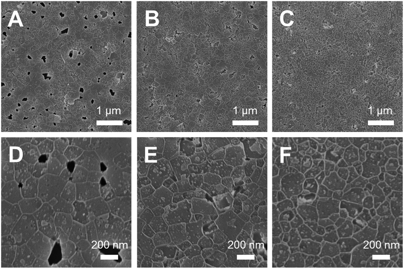 | ||
| Fig. 1 SEM images of tin perovskite thin films prepared by (A and D) a single antisolvent dripping after 20 s and slow heating to 70 °C, (B and E) a single antisolvent dripping after 20 s and directly placing the substrate on a 70 °C hot plate and (C and F) a double antisolvent dripping after 20 and 80 s and directly placing the substrate on a 70 °C hot plate. | ||
The X-ray diffractogram of a MA0.75FA0.15PEA0.1SnI3 perovskite film prepared with the optimized processing conditions reveals a typical pattern for a mixed 2D/3D tin perovskite with quasi-cubic/orthorhombic crystal structure (see Fig. 2A).8,16,28 The 100 and 200 peaks at 14.1 and 28.5° 2θ are very pronounced in the diffractogram, indicating a preferred orientation of the (h00) planes of the perovskite crystals parallel to the substrate. The weak peaks at 43.4 and 59.0° 2θ can be most likely assigned to the 300 and 400 planes. Moreover, two minor peaks at 13.6 and 27.4° 2θ are present in the diffractogram, which can be seen more clearly in Fig. S2,† where only the low intensity region of the diffractogram is shown. These are corresponding to slightly higher d values (6.51 and 3.25 Å) compared to the 100 and 200 peaks with d values of 6.28 and 3.13 Å, respectively. Thus, we assume that they can be correlated to a secondary phase exhibiting a slightly larger lattice spacing.
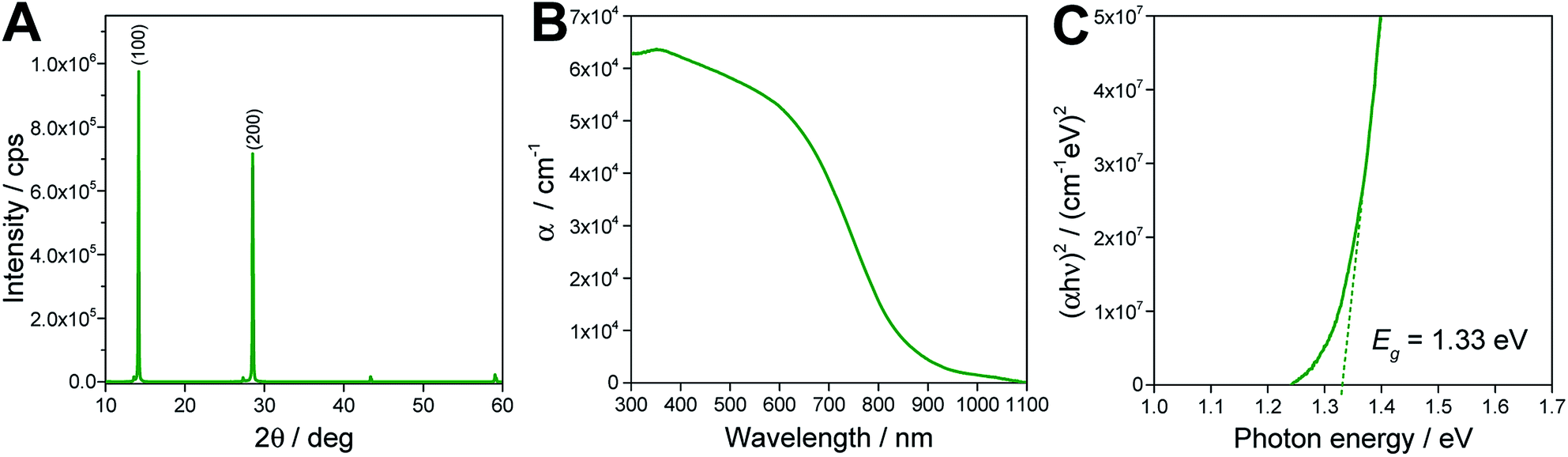 | ||
| Fig. 2 (A) X-ray diffraction pattern, (B) UV-Vis absorption spectrum and (C) Tauc plot of a MA0.75FA0.15PEA0.1SnI3 thin film on a glass substrate. | ||
The UV-Vis absorption spectrum of the film is depicted in Fig. 2B and reveals an absorption onset at approx. 1000 nm. Via the corresponding Tauc plot, a direct band gap of 1.33 eV is determined. The low band gap of this 2D/3D tin perovskite gives promise to obtain high photocurrents with this absorber material.
Next, we prepared solar cells with the optimized deposition conditions in the architecture glass/ITO/PEDOT:PSS/tin perovskite/PC60BM/Al (see Fig. 3A). The film thickness of the MA0.75FA0.15PEA0.1SnI3 absorber layers is around 225 nm as can be seen in the cross sectional SEM image in Fig. S1.† With this device setup, solar cells with PCEs up to 5.0% could be obtained in this study. The JV curves of a typical solar cell measured in forward direction are depicted in Fig. 3B. The solar cell exhibits a JSC of 18.4 mA cm−2, a VOC of 0.45 V and a FF of 0.61 leading to the PCE of 5.0%. Compared to the solar cells with the triple cation tin perovskite absorbers, double cation perovskite based devices with the compositions MA0.9PEA0.1SnI3, FA0.9PEA0.1SnI3, and MA0.75FA0.25SnI3, prepared with the same anti-solvent dripping procedure, revealed lower PCEs. While solar cells with MA0.9PEA0.1SnI3 absorber layers led to PCEs around 4.1%, the FA0.9PEA0.1SnI3 based solar cells revealed PCEs of 1.6%. The devices prepared with MA0.75FA0.25SnI3 perovskites only showed efficiencies of 0.4%. Typical JV curves and the average characteristic parameters are shown in Fig. S3, Tables S1 and S2 in the ESI.†
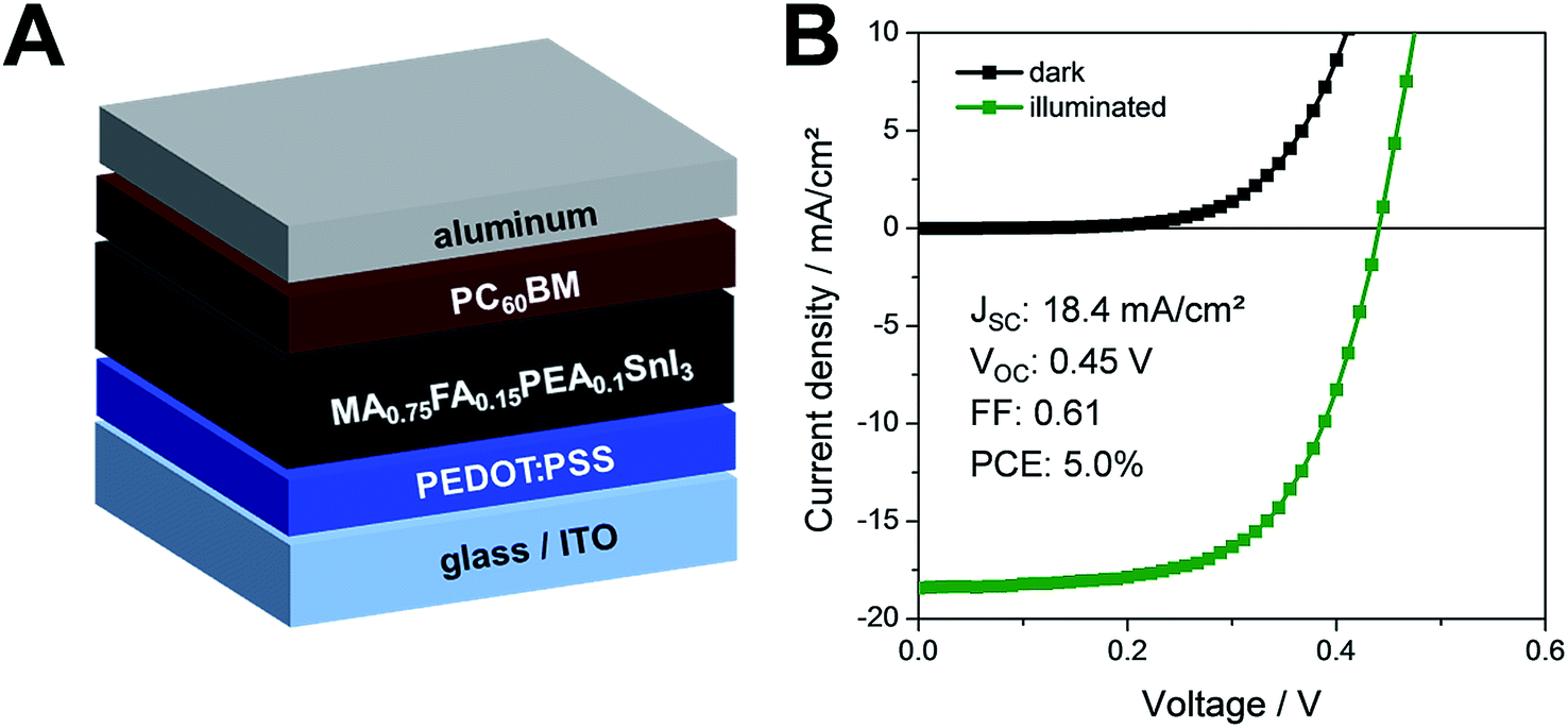 | ||
| Fig. 3 (A) Schematic of the used solar cell architecture, (B) JV curves of the tin perovskite solar cell with the highest PCE prepared within this study measured in forward scan direction 120 h after fabrication. | ||
To investigate charge recombination properties in the triple cation based tin perovskite solar cells, we studied the dependencies of JSC and VOC on the intensity of the incoming light. In Fig. 4A the power law dependence of JSC and light intensity (JSC ∝ Iα) is plotted and a value for α of 0.95 was extracted. This reveals the absence of space charge effects and only limited recombination of excited electrons prior to the collection at the electrodes. Fig. 4B shows the semi-logarithmic plot of VOCversus light intensity and from the graph an ideality factor n of 1.10 kT/q was extracted (k: Boltzmann constant, T: temperature of the solar cell, q: elementary charge). In general, the slope of VOCversus the natural logarithm of the light intensity is equal to 2 kT/q, if trap-assisted recombination is dominating. If bimolecular recombination is predominant, the slope is equal to 1 kT/q. Thus the value of 1.10 kT/q for the ideality factor n corroborates that bimolecular recombination is the dominant recombination mechanism and trap-mediated recombination processes play only a limited role. Similarly low ideality factors were found for a tin perovskite solar cell based on a 5-ammonium valeric acid/formamidinium double cation perovskite prepared with NH4Cl as additive in the precursor solution11 and for a FASnI3 based solar cell with a low dimensional perovskite interlayer between absorber and hole transport layer.28 Shao et al. reported an ideality factor of 1.2 kT/q for a solar cell with a FA/PEA-based mixed 2D/3D tin perovskite absorber layer.8
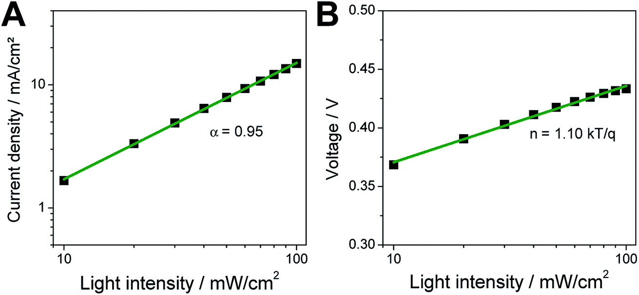 | ||
| Fig. 4 Dependencies of (A) JSC and (B) VOC on the light intensity. | ||
It is interesting to note that the α value of 0.95 is comparable to the values found for lead halide perovskite solar cells.29 Nevertheless, typical ideality factors n obtained for lead halide perovskite based devices are between 1.7 and 1.9 kT/q indicating trap-assisted recombination.29,30 However, Fei et al. reported a change of the ideality factor from 1.93 to 1.02 kT/q for lead perovskite solar cells by the addition of thiourea to the precursor solution and post processing of the perovskite films with ethyl acetate leading to a reduction of surface defect states.31
Moreover, the prepared solar cells show a stable shelf life over more than 5000 hours, as shown in Fig. 5. In this shelf life test, the solar cell was stored in a N2 filled glove box in ambient light conditions between the measurements. Up to 120 h after the fabrication we observed an increasing performance of the solar cells. A rise of the performance after some time of storage in inert conditions is a typical behaviour of tin perovskite solar cells and has been also already reported by others.7 Due to the initial increase in PCE, we normalized all the parameters shown in Fig. 5 to the values measured after 120 h. The VOC and FF show a very stable behaviour over time. The biggest changes are observed in the JSC, which increases up to 120 h after the fabrication of the solar cell. In the further course of the test, the JSC ranges between 85 and 100% of the maximum value. At the end of the testing period, after 5424 h, the solar cell has still a PCE of 4.7% which corresponds to 87% of the highest performance of this solar cell. To acquire a better overview about the stability of the solar cells, several more solar cells were tested over time. These solar cells also exhibited similarly good stability. The average values of the five best solar cells are shown in Table S3.†
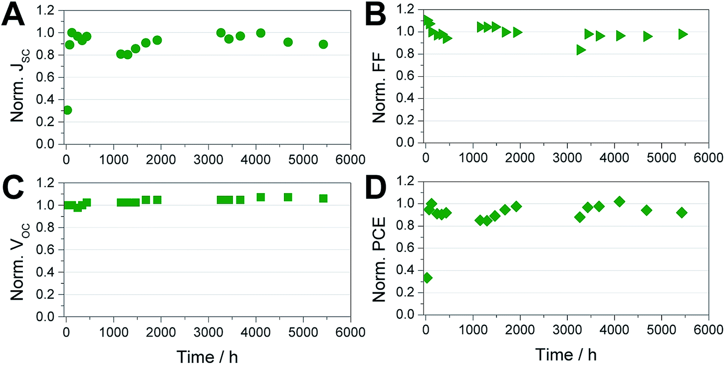 | ||
| Fig. 5 Characteristic parameters of the solar cell with the highest PCE prepared within this study measured over a time frame of 5424 h. The solar cell was stored in a N2 filled glove box in ambient light conditions during this period. | ||
At the end of the stability test, the solar cell was further characterized. As can be seen in the JV curves in Fig. 6A and the corresponding characteristic solar cell parameters in Table 1, the photocurrent is reduced from 18.4 to 15.5 mA cm−2 and the solar cell exhibits also a slight hysteresis. Moreover, as shown in Fig. S4,† the hysteresis properties of the solar cell vary slightly over time. While between day 136 and 195 the JV curves measured in forward and backward scan direction are almost overlapping, a certain hysteresis is observed before and afterwards in the stability test. From the JV curve at the end of the shelf life test measured in forward scan direction a PCE of 4.7% can be extracted, while scanning in backward direction leads to a PCE of 4.3%. The maximum power point tracking measurement reveals a steady-state PCE of 4.65% (see Fig. 6B). The external quantum efficiency (EQE) spectrum (Fig. 6C) matches well with the absorption spectrum of the absorber layer. An absorption spectrum of a MA0.75FA0.15PEA0.1SnI3 absorber layer with the same film thickness as used in the solar cells (225 nm) is shown in Fig. S5 in the ESI.† The onset of the EQE spectrum is already at 1000 nm, revealing a photocurrent generation over a broad spectral range, which can be considered as a major benefit of this MA-rich tin perovskite absorber investigated in this study and gives expectations for obtaining even higher photocurrents in future work.
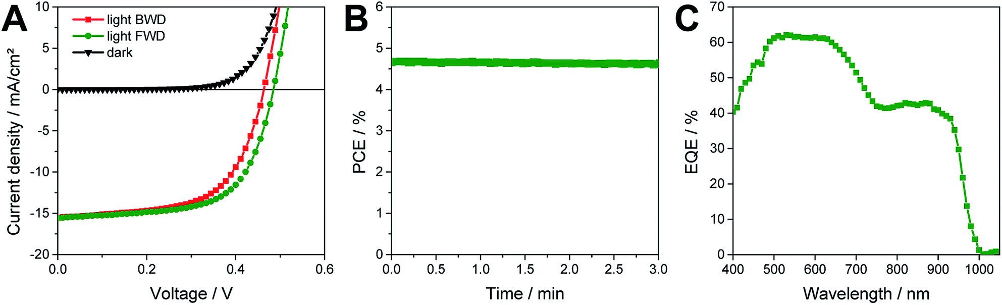 | ||
| Fig. 6 (A) JV curves after 5400 h of storage in a glove box measured with a 2.65 × 2.65 mm2 shadow mask in forward (FWD) and backward (BWD) scan direction; (B) maximum power point tracking measured with a shadow mask and (C) an EQE spectrum of this solar cell. | ||
Furthermore, the stability of the solar cells was investigated in ambient conditions. As expected, the non-encapsulated solar cells degrade within a few hours when exposed to air and humidity. The results are summarized in Fig. S6 and Table S4 in the ESI.† It is interesting to note that the PCE increased slightly within the first 1.5 hours of storage in ambient conditions. Afterwards, the solar cells degrade quickly and after 6.5 h a PCE of only 0.3% is retained.
However, due to the exceptional shelf life of these tin perovskite solar cells in inert conditions, we performed a further stability test under active load at maximum power point conditions and continuous illumination in inert atmosphere to simulate conditions which are near to real operation conditions of encapsulated photovoltaic devices.32 As can be seen in Fig. 7, over the period of the test of 72 hours (in particular in the first hours), the JMPP as well as the VMPP slightly increased which results not only in a stable behavior of the solar cell but even in a slight enhancement of the PCE from 3.5 to 4.1% during the continuous operation of the solar cell over 72 hours. We assume that the very limited trap-assisted recombination in these devices is a major pillar for the good shelf life and, in particular, also for the stable performance under continuous illumination and active load.33
 | ||
| Fig. 7 Results of a stability test performed in nitrogen atmosphere under continuous illumination and active load at the maximum power point; (A) JMPP, (B) light intensity, (C) VMPP, (D) PCE. Every 150th data point is shown. | ||
In conclusion, we could show that the amount of pinholes in the MA0.75FA0.15PEA0.1SnI3 perovskite layer can be significantly reduced by a double antisolvent dripping procedure combined with placing the substrate on a pre-heated hot plate directly after spin coating. The solar cells with these absorber layers revealed PCEs up to 5.0% and the solar cells show only minor trap-assisted recombination. Moreover, a good stability of the devices was observed in shelf life studies as well as a lifetime test under active load at the maximum power point and continuous illumination. In the shelf life test, the solar cell performance only diminished marginally from 5.0 to 4.7% after more than 5400 hours. The stability test under active load and continuous illumination even revealed a slight increase of the PCE during a period of more than 70 h. The time spans of the herein presented stability data are among the longest reported for tin perovskite-based solar cells so far and the observed results are very encouraging. In future work, we will conduct further stability tests under various testing conditions to gain more information about the stability of tin perovskite solar cells. Moreover, the impact of the optimized anti-solvent and annealing procedure on charge carrier densities in the perovskite, which is a further key to improving the performance as well as the stability of this absorber, is currently under investigation.
Experimental section
Sample and solar cell preparation
All chemicals and solvents were used as purchased without further purification unless otherwise noted. The solvents dimethylformamide (DMF), dimethyl sulfoxide (DMSO) and chlorobenzene (CB) were dried using molecular sieves (Carl Roth, 3 Å type 562 C). PEDOT:PSS was purchased from Heraeus (CLEVIOS™ P VP AI 4083), [6,6]-phenyl C61 butyric acid methyl ester (PC60BM) from Solenne, phenylethylammonium iodide (PEAI) from Greatcell Solar and aluminium from Kurt J. Lesker Company. All the other chemicals were purchased from Sigma Aldrich. Tin iodide (SnI2) with a purity of 99.99% was further purified in a tube furnace based on the different boiling points of tin(II) iodide and tin(IV) iodide. Under constant moderate N2 flow, the furnace is heated up to 380 °C within 30 minutes, kept at this temperature for 2 h and afterwards cooled down to room temperature.Patterned glass/ITO substrates (15 × 15 × 1.1 mm) (15 Ω sq−1) from Luminescence Technology Corp. were pre-cleaned with acetone, put in an isopropyl alcohol bath and placed into an ultrasonic bath at 40 °C for 30 minutes. The substrates were then dried in an N2 stream and further plasma etched for 3 minutes. PEDOT:PSS (used as purchased) was filtered through a 0.45 μm PVDF filter, then deposited by spin-coating at 3000 rpm for 60 s followed by annealing at 120 °C for 20 minutes. All steps were done outside of the glove box.
The perovskite precursor solution (1 M) was prepared by dissolving the corresponding amounts of MAI, FAI, PEAI, and SnI2 as well as 10 mol% SnF2 as additive in DMF/DMSO (4/1 vol%) to obtain the theoretical composition MA0.75FA0.15PEA0.1SnI3. The precursor solution was stirred overnight at room temperature under nitrogen atmosphere, followed by filtration through a 0.45 μm PTFE filter.
The precursor solution was spin-coated on the glass/ITO/PEDOT:PSS substrates at 5000 rpm for 60 s. After 20 s spinning time, 80 μl of CB were dropped on the spinning substrates to crystallize the perovskite, indicated by a color change from pale yellow to black. For the samples prepared with a double anti-solvent dripping, the second anti-solvent dripping (80 μl) was applied after 80 s and the spinning time was prolonged to 120 s. The perovskite films were then heated either from room temperature to 70 °C or directly placed on a 70 °C hot plate for 20 minutes. The solution for coating the electron transport layer – PC60BM (20 mg ml−1 in CB) – was stirred overnight at room temperature under inert conditions and filtered through a 0.45 μm PTFE filter before use. The solution was spin coated onto the absorber layer at 6000 rpm for 60 s. Afterwards, the top electrode (100 nm Al) was deposited by thermal evaporation under high vacuum conditions (<1 × 10⁻⁵ mbar) using a shadow mask (electrode area: 0.09 cm2).
Characterisation techniques
The MA0.75FA0.15PEA0.1SnI3 perovskite thin film was characterized by X-ray diffraction (XRD) with a PANalytical Empyrean system, which uses Cu Kα radiation. UV-Vis measurements of the perovskites were performed using a Perkin Elmer Lambda 35 UV/VIS spectrometer equipped with an integrating sphere. The optical data were recorded in the wavelength range of 300 to 1100 nm. Top view SEM images of the MA0.75FA0.15PEA0.1SnI3 perovskite thin films on glass/ITO/PEDOT:PSS were acquired on a Zeiss Supra 40 scanning electron microscope with an in-lens detector and 5 kV acceleration voltage.JV curves of all devices were recorded inside a glove box (nitrogen atmosphere) with a scan rate of 110 mV s−1 using a Keithley 2400 source meter connected to a LabView-based software. The solar cells were illuminated through a shadow mask (2.65 × 2.65 mm2) and the illumination (100 mW cm−2) was provided by a Dedolight DLH400 lamp, calibrated using a monocrystalline silicon WPVS reference solar cell from Fraunhofer ISE. For the illumination during the stability tests as well as for the light intensity dependent measurements of JSC and VOC, a white light (6500 K) 10 W chip-on-board high power LED was used. External quantum efficiency (EQE) measurements were acquired in inert atmosphere using a MuLTImode 4-AT monochromator (Amko) equipped with a 75 W xenon lamp (LPS 210-U, Amko), a lock-in amplifier (Stanford Research Systems, Model SR830), and a Keithley 2400 source meter. The monochromatic light was chopped at a frequency of 30 Hz and constant background illumination was provided by white light LEDs. The EQE spectra were measured in the wavelength range of 380–1050 nm (increment: 10 nm). The measurement setup was spectrally calibrated with a silicon photodiode (Newport Corporation, 818-UV/DB).
Conflicts of interest
There are no conflicts of interest to declare.Acknowledgements
This work was carried out within the project “Permasol” (FFG No. 848 929). The authors gratefully acknowledge financial support from the Austrian Climate and Energy Fund within the program Energy Emission Austria.References
- Z. Shi, J. Guo, Y. Chen, Q. Li, Y. Pan, H. Zhang, Y. Xia and W. Huang, Adv. Mater., 2017, 29, 1605005 CrossRef PubMed.
- S. F. Hoefler, G. Trimmel and T. Rath, Monatsh. Chem., 2017, 148, 795–826 CrossRef CAS PubMed.
- H. Hu, B. Dong and W. Zhang, J. Mater. Chem. A, 2017, 5, 11436–11449 RSC.
- A. D. Jodlowski, D. Rodríguez-Padrón, R. Luque and G. de Miguel, Adv. Energy Mater., 2018, 8, 1703120 CrossRef.
- M. Konstantakou and T. Stergiopoulos, J. Mater. Chem. A, 2017, 5, 11518–11549 RSC.
- W. Ke, C. C. Stoumpos and M. G. Kanatzidis, Adv. Mater., 2018, 1803230, DOI:10.1002/adma.201803230.
- E. Jokar, C. H. Chien, C. M. Tsai, A. Fathi and E. W.-G. Diau, Adv. Mater., 2019, 31, 1804835 CrossRef PubMed.
- S. Shao, J. Liu, G. Portale, H.-H. Fang, G. R. Blake, G. H. ten Brink, L. J. A. Koster and M. A. Loi, Adv. Energy Mater., 2018, 8, 1702019 CrossRef.
- Z. Zhao, F. Gu, Y. Li, W. Sun, S. Ye, H. Rao, Z. Liu, Z. Bian and C. Huang, Adv. Sci., 2017, 4, 1700204 CrossRef PubMed.
- F. Wang, X. Jiang, H. Chen, Y. Shang, H. Liu, J. Wei, W. Zhou, H. He, W. Liu and Z. Ning, Joule, 2018, 2, 2732–2743 CrossRef CAS.
- H. Xu, Y. Jiang, T. He, S. Li, H. Wang, Y. Chen, M. Yuan and J. Chen, Adv. Funct. Mater., 2019, 1807696, DOI:10.1002/adfm.201807696.
- E. Jokar, C.-H. Chien, A. Fathi, M. Rameez, Y.-H. Chang and E. W.-G. Diau, Energy Environ. Sci., 2018, 11, 2353–2362 RSC.
- W. Liao, D. Zhao, Y. Yu, C. R. Grice, C. Wang, A. J. Cimaroli, P. Schulz, W. Meng, K. Zhu, R.-G. Xiong and Y. Yan, Adv. Mater., 2016, 28, 9333–9340 CrossRef CAS PubMed.
- N. K. Noel, S. D. Stranks, A. Abate, C. Wehrenfennig, S. Guarnera, A.-A. Haghighirad, A. Sadhanala, G. E. Eperon, S. K. Pathak, M. B. Johnston, A. Petrozza, L. M. Herz and H. J. Snaith, Energy Environ. Sci., 2014, 7, 3061–3068 RSC.
- F. Hao, C. C. Stoumpos, D. H. Cao, R. P. H. Chang and M. G. Kanatzidis, Nat. Photonics, 2014, 8, 489–494 CrossRef CAS.
- Y. Liao, H. Liu, W. Zhou, D. Yang, Y. Shang, Z. Shi, B. Li, X. Jiang, L. Zhang, L. N. Quan, R. Quintero-Bermudez, B. R. Sutherland, Q. Mi, E. H. Sargent and Z. Ning, J. Am. Chem. Soc., 2017, 139, 6693–6699 CrossRef CAS PubMed.
- H. Tsai, W. Nie, J.-C. Blancon, C. C. Stoumpos, R. Asadpour, B. Harutyunyan, A. J. Neukirch, R. Verduzco, J. J. Crochet, S. Tretiak, L. Pedesseau, J. Even, M. A. Alam, G. Gupta, J. Lou, P. M. Ajayan, M. J. Bedzyk, M. G. Kanatzidis and A. D. Mohite, Nature, 2016, 536, 312–316 CrossRef CAS PubMed.
- S. J. Lee, S. S. Shin, Y. C. Kim, D. Kim, T. K. Ahn, J. H. Noh, J. Seo and S. I. Seok, J. Am. Chem. Soc., 2016, 138, 3974–3977 CrossRef CAS PubMed.
- F. Hao, C. C. Stoumpos, P. Guo, N. Zhou, T. J. Marks, R. P. H. Chang and M. G. Kanatzidis, J. Am. Chem. Soc., 2015, 137, 11445–11452 CrossRef CAS PubMed.
- X. Liu, K. Yan, D. Tan, X. Liang, H. Zhang and W. Huang, ACS Energy Lett., 2018, 3, 2701–2707 CrossRef CAS.
- T. Fujihara, S. Terakawa, T. Matsushima, C. Qin, M. Yahiro and C. Adachi, J. Mater. Chem. C, 2017, 5, 1121–1127 RSC.
- J. Liu, M. Ozaki, S. Yakumaru, T. Handa, R. Nishikubo, Y. Kanemitsu, A. Saeki, Y. Murata, R. Murdey and A. Wakamiya, Angew. Chem., Int. Ed., 2018, 57, 13221–13225 CrossRef CAS PubMed.
- H. Kim, Y. H. Lee, T. Lyu, J. H. Yoo, T. Park and J. H. Oh, J. Mater. Chem. A, 2018, 6, 18173–18182 RSC.
- J. Qiu, Y. Xia, Y. Chen and W. Huang, Adv. Sci., 2019, 6, 1800793 CrossRef PubMed.
- Z. Zhu, C. C. Chueh, N. Li, C. Mao and A. K. Y. Jen, Adv. Mater., 2018, 30, 1703800 CrossRef PubMed.
- W. Ke, C. C. Stoumpos, M. Zhu, L. Mao, I. Spanopoulos, J. Liu, O. Y. Kontsevoi, M. Chen, D. Sarma, Y. Zhang, M. R. Wasielewski and M. G. Kanatzidis, Sci. Adv., 2017, 3, e1701293 CrossRef PubMed.
- S. Gupta, D. Cahen and G. Hodes, J. Phys. Chem. C, 2018, 122, 13926–13936 CrossRef CAS.
- K. Chen, P. Wu, W. Yang, R. Su, D. Luo, X. Yang, Y. Tu, R. Zhu and Q. Gong, Nano Energy, 2018, 49, 411–418 CrossRef CAS.
- T. Singh and T. Miyasaka, Adv. Energy Mater., 2018, 8, 1700677 CrossRef.
- G.-J. A. H. Wetzelaer, M. Scheepers, A. M. Sempere, C. Momblona, J. Ávila and H. J. Bolink, Adv. Mater., 2015, 27, 1837–1841 CrossRef CAS PubMed.
- C. Fei, B. Li, R. Zhang, H. Fu, J. Tian and G. Cao, Adv. Energy Mater., 2017, 7, 1602017 CrossRef.
- M. O. Reese, S. A. Gevorgyan, M. Jørgensen, E. Bundgaard, S. R. Kurtz, D. S. Ginley, D. C. Olson, M. T. Lloyd, P. Morvillo, E. A. Katz, A. Elschner, O. Haillant, T. R. Currier, V. Shrotriya, M. Hermenau, M. Riede, K. R. Kirov, G. Trimmel, T. Rath, O. Inganäs, F. Zhang, M. Andersson, K. Tvingstedt, M. Lira-Cantu, D. Laird, C. McGuiness, S. Gowrisanker, M. Pannone, M. Xiao, J. Hauch, R. Steim, D. M. DeLongchamp, R. Rösch, H. Hoppe, N. Espinosa, A. Urbina, G. Yaman-Uzunoglu, J.-B. Bonekamp, A. M. van Breemen, C. Girotto, E. Voroshazi and F. C. Krebs, Sol. Energy Mater. Sol. Cells, 2011, 95, 1253–1267 CrossRef CAS.
- J. Chen and N.-G. Park, Adv. Mater., 2018, 1803019, DOI:10.1002/adma.201803019.
Footnote |
| † Electronic supplementary information (ESI) available: Additional photovoltaic performance parameters, JV curves, XRD and SEM data, UV-Vis absorption spectra. See DOI: 10.1039/c9ta02835h |
| This journal is © The Royal Society of Chemistry 2019 |