
A robust CdS/In2O3 hierarchical heterostructure derived from a metal–organic framework for efficient visible-light photocatalytic hydrogen production†
Jia-Tong
Ren
,
Kun
Yuan
,
Ke
Wu
,
Liang
Zhou
and
Ya-Wen
Zhang
 *
*
Beijing National Laboratory for Molecular Sciences, State Key Laboratory of Rare Earth Materials Chemistry and Applications, PKU-HKU Joint Laboratory in Rare Earth Materials and Bioinorganic Chemistry, College of Chemistry and Molecular Engineering, Peking University, Beijing 100871, China. E-mail: ywzhang@pku.edu.cn
First published on 5th December 2018
Abstract
Building sulfide/oxide heterostructure photocatalysts is not only beneficial for the separation and transfer of photo-generated carriers in photocatalytic reactions but also an effective means of broadening the light absorption range of oxides by introducing narrow-bandgap sulfides. However, the construction of highly-efficient sulfide/oxide heterostructures with intimate and extensive contact between different components for visible-light photocatalytic hydrogen production remains a challenge. Herein, a novel sulfide/oxide heterostructure of CdS/In2O3 hierarchical nanotubes was synthesized starting from a metal–organic framework (MOF). In such a heterostructure, CdS and In2O3 are integrated by close contact of corresponding small nanoparticles, which is beneficial for the separation and transfer of photo-generated charge carriers. Benefiting from the intimate interface, suitable energy band structure, as well as the inherent advantages of MOFs-derived nanomaterials, the optimal CdS/In2O3 hierarchical nanotubes showed the best activity in visible-light photocatalytic hydrogen production without any cocatalysts, which was 78.6 times and 16.9 times higher than activities of In2O3 hierarchical nanotubes and CdS nanoparticles, respectively.
Introduction
In today's society, the ever-growing energy demand has become a major factor restricting the progress of human civilization. As the main energy source nowadays, fossil fuels are increasingly exhausted and new and sustainable energy resources are necessary.1–7 Hydrogen production by photocatalytic water splitting is a potential strategy to convert solar energy to chemical storable and clean energy of hydrogen.8–11 As a result, such a technique has attracted extensive attention to addressing the increasingly severe energy crisis. The key challenge for scientists is to develop efficient and stable photocatalysts. Up till now, various kinds of semiconductor photocatalysts, such as metal oxides (e.g. TiO2![[thin space (1/6-em)]](https://www.rsc.org/images/entities/char_2009.gif) 12–15 and SrTiO316–18), metal nitrides (e.g. Ta3N519,20 and WN21), metal sulfides (e.g. CuxS22,23 and CdS24–28) and metal-free carbon nitrides,29–36 have been developed and applied in the field of solar-driven water splitting to produce hydrogen fuels. However, the photocatalytic efficiency of hydrogen production is still far lower than expected. In order to enhance the efficiency of photocatalytic reactions, various methods of catalyst preparation have been tried, including nanostructuralization,37–40 doping of heteroatoms,41–44 using cocatalysts,45–48 building of heterostructures49–51 and so on. Among them, building heterostructures is a rapid and effective method to promote photocatalytic efficiency of hydrogen production.
12–15 and SrTiO316–18), metal nitrides (e.g. Ta3N519,20 and WN21), metal sulfides (e.g. CuxS22,23 and CdS24–28) and metal-free carbon nitrides,29–36 have been developed and applied in the field of solar-driven water splitting to produce hydrogen fuels. However, the photocatalytic efficiency of hydrogen production is still far lower than expected. In order to enhance the efficiency of photocatalytic reactions, various methods of catalyst preparation have been tried, including nanostructuralization,37–40 doping of heteroatoms,41–44 using cocatalysts,45–48 building of heterostructures49–51 and so on. Among them, building heterostructures is a rapid and effective method to promote photocatalytic efficiency of hydrogen production.
Building heterostructure photocatalysts is a versatile means of promoting the separation and transfer of photo-generated carriers through the interface in photocatalytic reactions.49–51 On this basis, the construction of sulfide/oxide heterostructures is also in favour of broadening light absorption range of oxides by introducing narrow-bandgap sulfides, thus, obtaining highly-efficient photocatalysts with relatively high stability and low cost. Although diverse sulfide/oxide heterostructure photocatalysts have been designed and synthesized,52–55 many of them do not show remarkable enhancement towards visible-light photocatalytic hydrogen production without cocatalysts. This may be primarily caused by deficient interfaces of two or more components in photocatalysts as a result of large bulk volume or unreasonable contact forms.
Based on the above considerations, MOFs (metal–organic frameworks) derived heterostructures for photocatalysis have been widely studied in recent years.55–58 Such heterostructures can often inherit the porous structure of original MOFs and own a lot of advantages. First, such hierarchical structures with interior voids can enhance light harvesting by extensive reflection and scattering of incident light.9 Secondly, the heterostructures are composed of small nanosized subunits, offering more exposed active sites owing to large specific surface areas. Moreover, nanosized building blocks make it possible to realize intimate and extensive contact between two or more semiconductor components, which makes photo-induced carriers separate and transfer to the surface more efficiently. In recent years, MOFs-derived sulfides or sulfide/sulfide heterostructure photocatalysts for solar-to-chemical energy conversion have been widely studied.59–62 In particular, the Lou's group have recently developed two In-MOF-derived hierarchical tubular heterostructures (In2S3/CdIn2S461 and ZnIn2S4/In2O355) for efficient visible-light CO2 photoreduction. Their research provides new ideas for designing heterostructure photocatalysts. However, MOFs-derived high-efficiency sulfide/oxide heterostructures for visible-light photocatalytic hydrogen production have rarely been studied and need to be further explored.
From another perspective, In2O3 is a common oxide semiconductor in visible-light photocatalysis with a bandgap of around 2.8 eV.39,63–65 Although various In2O3-based heterostructures for photocatalytic hydrogen production have been synthesized, including Cr-doped Ba2In2O5/In2O3,66 Gd2Ti2O7/In2O3,67 In2O3/La2Ti2O7,68 In2O3/ZnO,69 In2O3/g-C3N4,70 In2S3/In2O353 and In2S3/CdIn2S4/In2O3,71 most of them can only boost the activity of In2O3 by no more than 30 times, even in the presence of Pt cocatalyst. On the other hand, as an efficient narrow-bandgap photocatalyst for hydrogen production, CdS suffers from low photostability and rapid recombination of photo-induced charge carriers.24–28 It has been found in recent years that building heterostructures72,73 or phase junctions,74 homoepitaxial growth on CdS nanocrystals,75 using cocatalysts (e.g. Pt76 and Co(II)/Ni(II) species25), designing delicate porous nanostructures77 as well as employing a redox shuttle for hole transfer78 can help to solve these problems, especially low photostability of CdS. As a result, more and more 0D, 1D and 2D CdS-based heterostructures have been used for photocatalytic hydrogen production recently,79,80 including graphene–CdS–MoS2 composites,81 CdS@MoS2 core–shell nanowires82 and so on. These heterostructures all showed huge promotion in photocatalytic activity and stability. In other words, CdS has become a potential candidate for the construction of efficient hydrogen production photocatalysts. Nevertheless, few attempts have been made to combine In2O3 with CdS to construct heterostructure photocatalysts, not to mention that the interfacial effect of In2O3 and CdS in photocatalytic hydrogen production has never been studied in the absence of cocatalysts.83
Taking all the above into account, herein, we synthesized a novel sulfide/oxide heterostructure of CdS/In2O3 hierarchical nanotubes by a facile two-step method, that is, the formation of In2O3 hierarchical nanotubes by calcination of an In-MOF (MIL-68) followed by in situ growth of CdS nanoparticles via hydrolysis of thioacetamide (as illustrated in Scheme 1). In such a heterostructure, CdS and In2O3 are integrated by close contact of corresponding small nanoparticles, which is beneficial to the separation and transfer of photo-generated charge carriers. In consequence, the optimal CdS/In2O3 hierarchical nanotubes showed the best activity in visible-light photocatalytic hydrogen production without any cocatalysts, which was 78.6 times and 16.9 times greater than activities of In2O3 hierarchical nanotubes and CdS nanoparticles, respectively.
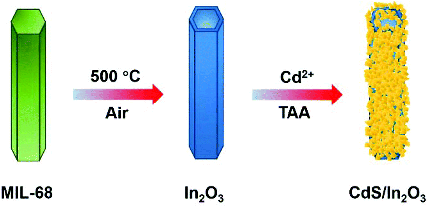 | ||
| Scheme 1 Schematic of the synthesis process of CdS/In2O3 hierarchical nanotubes. | ||
Experimental section
Chemicals
In(NO3)3·xH2O (A.R., Aladdin), anhydrous InCl3 (A.R., Sinopharm Chemical Reagent Co. Ltd, China), urea (A.R., Xilong Chemical Co. Ltd, China), polyvinylpyrrolidone (PVP, Mw = 58000, A.R., Aladdin), terephthalic acid (H2BDC, A.R., Sigma-Aldrich), CdCl2·2.5H2O (A.R., Sinopharm Chemical Reagent Co. Ltd, China), thioacetamide (TAA, A.R., Sinopharm Chemical Reagent Co. Ltd, China), N,N-dimethylformamide (DMF, A.R., Xilong Chemical Co. Ltd, China), triethanolamine (TEOA, A.R., Beijing Tongguang Fine Chemicals Company), ethanol (A.R.) and deionized water (Millipore, 18.2 MΩ cm) were used as received.
Synthesis of In2O3 hierarchical nanotubes
The MIL-68 hexagonal prisms were first synthesized according to a reported oil bath method with some modifications.84 Briefly, 468 mg of In(NO3)3·xH2O and 180 mg of H2BDC were dissolved in 54 mL of DMF under continuous stirring for 15 min, followed by reacting in an oil bath (100 °C) for 1.5 h. After the resulting mixture was cooled to room temperature, the white precipitate was collected by centrifugation, washed with DMF and ethanol several times, and finally dried in vacuum at 50 °C. The In2O3 nanotubes with a light yellow color were finally obtained by calcining the MIL-68 hexagonal prisms in air at 500 °C for 2 h with a heating rate of 5 °C min−1.Synthesis of CdS/In2O3 hierarchical nanotubes
The in situ growth of CdS based on In2O3 hierarchical nanotubes was achieved through the hydrolysis of TAA. In particular, 40 mg of In2O3 nanotubes were dispersed in 20 mL of H2O by sonication, and 1.6 mL of CdCl2 solution (1 mol L−1) was added. After stirring for 20 min, 20 mL of aqueous solution containing 240 mg TAA was added and the mixture was stirred for another 10 min. Finally, the mixture was placed into an oil bath (70 °C) and kept for 4 h. The orange-yellow product (denoted as CdS/In2O3-2 or CI-2 for short) was collected by centrifugation, washed with H2O and ethanol several times, and dried in vacuum at 40 °C. CdS/In2O3-1 (CI-1) and CdS/In2O3-3 (CI-3) were synthesized using the same procedure as that for CdS/In2O3-2, except 0.75 and 1.25 times the amount of precursors in the growth step of CdS (including CdCl2 solution and TAA) were used, respectively.Synthesis of CdS nanoparticle aggregates
300 mg of TAA was dissolved in 50 mL of H2O, followed by the addition of 2 mL of CdCl2 solution (1 mol L−1). The solution was placed into an oil bath (70 °C) and kept for 8 h. The orange product was collected by centrifugation, washed with H2O and ethanol several times, and finally dried in vacuum at 40 °C.Synthesis of In2O3 nanorods
In2O3 nanorods were synthesized according to a reported hydrothermal method.53 100 mg of InCl3, 400 mg of urea and 800 mg of PVP were dissolved in 15 mL of H2O with continuous stirring. The solution was then transferred to a 25 mL Teflon-lined stainless steel autoclave and heated at 100 °C for 24 h. After the mixture was cooled to room temperature, the white precursor was collected by centrifugation, washed with H2O and ethanol several times, and dried in vacuum at 50 °C. The In2O3 nanorods with a light yellow color were finally obtained by calcining the precursor in air at 350 °C for 2 h at a heating rate of 5 °C min−1.Synthesis of CdS/In2O3 nanorods
The synthesis of CdS/In2O3 nanorods (denoted as CIR-2 for short) was the same as that of CdS/In2O3-2 (CI-2), except that In2O3 nanorods rather than hierarchical nanotubes were used.Characterization
Transmission electron microscopy (TEM), high-resolution transmission electron microscopy (HRTEM), high-angle annular dark-field scanning transmission electron microscopy (HAADF-STEM) and energy-dispersive X-ray spectroscopy (EDS) were carried out using FEG-TEM (JEM-2100F, JEOL, Japan) operated at 200 kV. Scanning electron microscopy (SEM) was carried out using a FE-SEM (Hitachi S-4800, Japan). X-ray diffraction (XRD) patterns were obtained on a D/MAX-2000 diffractometer (Rigaku, Japan) using Cu-Kα radiation. Inductively coupled plasma-atomic emission spectroscopy (ICP-AES) analysis was performed on a Profile Spec ICP-AES spectrometer (Leeman, USA). X-ray photoelectron spectroscopy (XPS) analysis was performed on an Axis Ultra XPS spectrometer (Kratos, U.K.). The C 1s line at 284.8 eV was used to calibrate the binding energies. Nitrogen adsorption–desorption isotherm experiments were performed at 77 K on an Accelerated Surface Area & Porosimetry system (ASAP 2010, Micromeritics, USA) to determine the Brunauer–Emmett–Teller (BET) surface area and pore size distribution. UV-vis diffuse reflectance spectra (UV-vis DRS) were acquired using a UV-3600 Plus UV-vis-NIR spectrometer (Shimadzu, Japan) equipped with an integrating sphere, and BaSO4 was used as a reference. Photoluminescence (PL) spectra were obtained using a FLS980 steady-state and time-resolved fluorescence spectrometer (Edinburgh Instruments, U.K.) at room temperature. The excitation wavelength was 300 nm for steady-state PL. Time-resolved PL decay spectra were recorded at 545 nm under the excitation of a 375 nm laser source.Electrochemical measurements were performed in a standard three-electrode system. The electrolyte was Na2SO4 solution (0.5 M, pH ∼ 6.1). A Pt plate and a KCl-saturated Ag/AgCl electrode were used as the counter and the reference electrode, respectively. The working electrode was prepared as described below. First, the as-prepared photocatalyst was dispersed in a mixed solvent of H2O, ethanol and Nafion (8:2:1 by volume) to form a suspension with a concentration of ca. 9 mg mL−1. Then 35 μL of the suspension was dropped onto a fixed area (ca. 0.2826 cm2) of an ITO glass. Finally, the ITO glass was naturally dried to obtain the working electrode. Transient photocurrents were measured at 0.6 V (vs. Ag/AgCl) using a 300 W Xe lamp (with an intensity of ca. 100 mW cm−2) as a light source. Electrochemical impedance spectroscopy (EIS) measurements were performed at a potential of 0.3 V (vs. Ag/AgCl) and an amplitude of 10 mV. The frequency range was from 100 kHz to 10 mHz. Mott-Schottky tests were conducted with different frequencies of 0.5, 1 and 2 kHz in the dark.
Photocatalytic hydrogen production from water
A quartz photoreactor attached to a closed photocatalytic system equipped with an online gas chromatograph (GC-7806) was used to evaluate the activity of photocatalytic hydrogen production. 20 mg of the catalyst was suspended in a mixture of 72 mL of H2O and 8 mL of TEOA. The temperature of the reactor was kept at 288 K by circulating cooling water. Before light irradiation, the system was evacuated several times to remove the air inside. Then the reactor was illuminated by a 300 W Xe lamp (Microsolar 300, PerfectLight) equipped with a UV cut-off filter (λ > 400 nm). The light intensity was approximately 500 mW cm−2. Hydrogen was detected by a thermal conductivity detector (TCD) and Ar was used as the carrier gas.The apparent quantum efficiency (AQE) of photocatalysts was measured using a monochromatic irradiation light of 420 nm by a 300 W Xe lamp equipped with a band-pass filter. The AQE was calculated as follows:
Results and discussion
Synthesis, characterization and photocatalytic activity towards hydrogen production
In the first synthesis step, In2O3 hierarchical nanotubes were formed after the calcination of the MIL-68 hexagonal prisms. For In2O3 hierarchical nanotubes and CdS nanoparticle aggregates, all the main diffraction peaks in the XRD patterns (Fig. S1a and S1b†) are indexed to cubic In2O3 (JCPDS no. 01-089-4595) and hexagonal CdS (JCPDS no. 00-041-1049). After the growth of CdS, XRD patterns of the as-prepared CdS/In2O3 heterostructures are presented in Fig. 1. For all heterostructures, the diffraction peaks reveal the features of both cubic In2O3 and hexagonal CdS without obvious impurities such as In2S3. Moreover, the peak intensity ratio of CdS to In2O3 in the heterostructures increases in the order of CdS/In2O3-1, CdS/In2O3-2 and CdS/In2O3-3, which is in accordance with the variation trend of weight ratio of CdS and In2O3 obtained by ICP-AES analysis (ca. 0.375, 0.709 and 0.952 for CdS/In2O3-1, CdS/In2O3-2 and CdS/In2O3-3).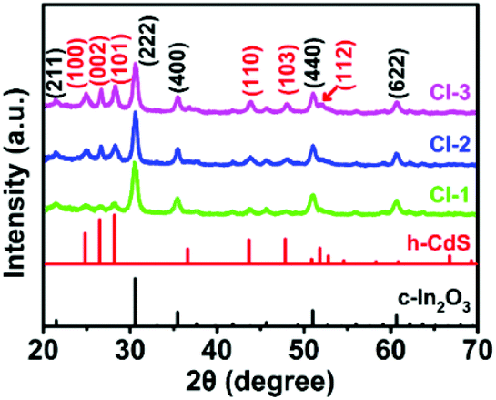 | ||
| Fig. 1 XRD patterns of the as-prepared CdS/In2O3 heterostructures. | ||
SEM images of the MIL-68 hexagonal prisms are shown in Fig. S2.† From the SEM image shown in Fig. 2a, the as-prepared In2O3 by the calcination of MIL-68 are nanotubes in shape, with a width of 1 micrometer around and a length of several micrometers for most nanotubes. By close observation of the magnified SEM image (Fig. 2b), it can be found that the surface of the In2O3 nanotubes is not integrated. On the contrary, the In2O3 nanotubes are made up of small nanoparticles, as a result of which a slight unevenness of the surface is observed. The TEM image in Fig. 2c confirms such tubular morphology. Compared with the interior of the In2O3 nanotubes, higher contrast for the edge reflects the hollow feature of nanotubes. As illustrated by magnified TEM image of the nanotube mouth (Fig. 2d), the constituent nanoparticles are approximately two dozen nanometers with irregular shapes. Furthermore, the distinct lattice fringes from the HRTEM image (Fig. 2e) show that the as-prepared In2O3 nanotubes are well crystallized after heat treatment of the In-MOF. The inter-planar distances of about 0.411 nm, 0.291 nm and 0.250 nm correspond to the (211), (222) and (400) crystal planes of cubic In2O3, respectively.
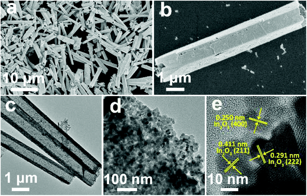 | ||
| Fig. 2 (a, b) SEM, (c, d) TEM and (e) HRTEM images of In2O3 nanotubes. | ||
As the surface of the In2O3 nanotubes is negatively charged, proven by negative zeta potential (Fig. S3†), Cd2+ can be adsorbed by the In2O3 nanotubes through electrostatic interactions85 and then react with a sulfur source to form CdS. After the growth of CdS, the as-obtained CdS/In2O3 nanotubes experience noticeable changes in morphology. As shown in Fig. 3a and b, the inner and outer surfaces of CdS/In2O3-2 are quite rough compared with In2O3 nanotubes, although the tubular shape remains unchanged. CdS/In2O3-1 and CdS/In2O3–3 show similar morphology, except with different degrees of roughness (Fig. S4†). The TEM image in Fig. 3c further validates such a change. The edges of In2O3 nanotubes are obviously uneven with nanoparticles different from In2O3 nanoparticles in shape (shown in Fig. 3d). In addition, the arrangement of nanoparticles in the structure of nanotubes becomes more compact, indicating that the as-grown CdS nanoparticles are in close proximity to In2O3 nanoparticles in the CdS/In2O3 nanotubes. SEM images of CdS/In2O3-2 at different time in the growth process of CdS are shown in Fig. S5.† It is evident that the nanotube morphology of In2O3 is unchanged during the formation process of CdS nanoparticles. While pure CdS is composed of agglomerates as large as several micrometers, which, in turn, are composed of nanoparticles (Fig. S6†), the CdS nanoparticles in CdS/In2O3 nanotubes are apparently more dispersive. Such a phenomenon reveals that In2O3 nanotubes are ideal supports for the decentralized growth of CdS nanoparticles without the assistance of surfactants. This may be beneficial to the enhancement of surface area and the exposure of more active sites compared with pure CdS. To verify the combination of CdS and In2O3, HRTEM characterization was carried out (Fig. 3e). The lattice fringes corresponding to (100) and (002) crystal planes of hexagonal CdS can be found around In2O3 nanoparticles, reflecting the formation of CdS/In2O3 heterostructure to some extent. In addition, two sets of diffraction fringes, belonging to In2O3 and CdS in selected area electron diffraction (SAED) pattern (Fig. S7†), support the formation of CdS/In2O3 heterostructure. Elemental mapping was conducted to further show that In, Cd and S are evenly distributed in the heterostructure (Fig. 3f). Moreover, the line scan result in Fig. 3g not only verifies the hollow feature of CdS/In2O3 nanotubes again, but also shows uniform variation tendency of the element In, Cd and S. Elemental mapping and line scan both lead to the fact that homogeneous CdS/In2O3 heterostructure can be obtained by in situ growth of CdS nanoparticles on the basis of In2O3 nanotubes. In such a hierarchical heterostructure, CdS and In2O3 are integrated by close contact of corresponding small nanoparticles, which ensures large interfaces of these two semiconductor components. Compared to other CdS/In2O3 photocatalysts, no templates86 or substrates87 were used in our synthetic procedure. In addition, in situ growth of CdS means that we did not need to pre-synthesize CdS nanoparticles and combine these two semiconductor nanostructures using an extra step.83 As a whole, our synthetic procedure was simplified to a great extent.
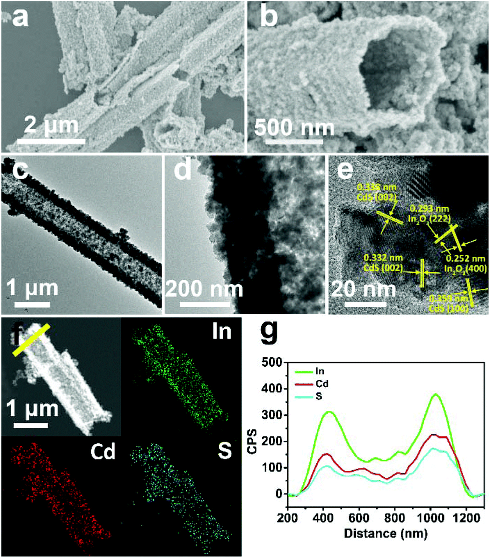 | ||
| Fig. 3 (a, b) SEM, (c, d) TEM, (e) HRTEM and (f) HAADF-STEM and EDS mapping images of CdS/In2O3-2; (g) EDS line scan profiles of CdS/In2O3-2 obtained along the yellow line in (f). | ||
X-ray photoelectron spectroscopy (XPS) analysis was performed to determine the chemical composition and valence states of the elements in CdS/In2O3-2. The survey-scan spectrum of CdS/In2O3-2 (Fig. S8†) reveals the existence of In, O, Cd, S and C on the surface and sub-surface of CdS/In2O3 nanotubes. For In 3d core-level spectrum (Fig. 4a), two peaks centered at 452.1 and 444.5 eV correspond to In 3d3/2 and In 3d5/2 peaks of In3+, respectively.55,66 It is noteworthy that the peak positions of In 3d3/2 and In 3d5/2 for pure In2O3 are 451.6 eV and 444.0 eV, respectively. The binding energy shift of ca. 0.5 eV means that the chemical environment of Indium in In2O3 nanotubes has been changed after the formation of CdS/In2O3 heterostructure, reflecting the strong interaction between CdS and In2O3 in their interfacial zone.71,88 For the O 1s core-level spectrum (Fig. 4b), the peak positioned at 530.0 eV is attributed to the lattice oxygen, while the peak positioned at 531.8 eV is attributed to the surface hydroxyl oxygen.88,89 The Cd 3d high resolution XPS spectrum (Fig. 4c) shows two peaks at 412.4 and 405.6 eV, which are assigned to Cd 3d3/2 and Cd 3d5/2 peaks of Cd2+, respectively.90,91 As for S 2p spectrum (Fig. 4d), two peaks at 163.2 and 162.0 eV are respectively ascribed to S 2p1/2 and S 2p3/2 peaks of S2−.91 The binding energies of Cd and S are in good agreement with a previous report about CdS nanoparticles,91 indicating the successive introduction of CdS in our heterostructure. All the above XPS results further confirm the formation of CdS/In2O3 heterostructure.
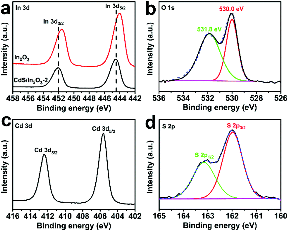 | ||
| Fig. 4 High resolution XPS spectra of (a) In 3d, (b) O 1s, (c) Cd 3d and (d) S 2p in CdS/In2O3-2. The red curve in (a) is the high resolution XPS spectrum of In 3d in In2O3 nanotubes. | ||
UV-vis diffuse reflectance spectra (UV-vis DRS) can reflect the optical absorption property of semiconductors. Fig. 5a depicts the DRS of In2O3, CdS and CdS/In2O3 heterostructures. Moreover, band gap energy (Eg) of the samples can be estimated utilizing Tauc plots: (αhν)1/r = C(hν − Eg), where α, ν and C are the absorption coefficient, light frequency and a constant, respectively; r is 1/2 (for direct band gap semiconductors) or 2 (for indirect band gap semiconductors). The results are shown in Fig. S9.† Pure In2O3 nanotubes mainly absorb UV light (λ < 400 nm) and are nearly incapable of absorbing visible light with a wavelength greater than 500 nm, which is unfavourable for visible-light photocatalysis. Eg of In2O3 nanotubes is estimated to be 2.75 eV. In contrast, pure CdS has a wider absorption range in the visible region and its Eg is only 2.25 eV. For all CdS/In2O3 heterostructures, the light absorption capacity is very close to that of CdS (Eg = 2.30 eV, 2.28 eV and 2.23 eV for CdS/In2O3-1, CdS/In2O3-2 and CdS/In2O3-3, respectively), which is undoubtedly an advantage compared with pure In2O3 nanotubes.
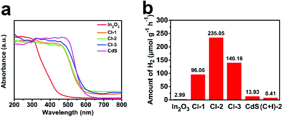 | ||
| Fig. 5 (a) UV-vis DRS of In2O3, CdS and CdS/In2O3 heterostructures; (b) photocatalytic activities of different samples towards visible-light hydrogen production from water. | ||
The activities of different samples for visible-light photocatalytic hydrogen production are shown in Fig. 5b. All the photocatalytic tests were performed without the assistance of cocatalysts. For pure In2O3 nanotubes and CdS nanoparticle aggregates, the activities were fairly low, which is mainly attributed to fast recombination of photo-generated electron–hole pairs in single-component semiconductor photocatalysts. In addition, weak light absorption ability of In2O3 nanotubes (shown in Fig. 5a) and obvious aggregation of CdS nanoparticles (shown in Fig. S6†) become their respective constraints. Intriguingly, for all CdS/In2O3 hierarchical nanotubes, significant photocatalytic activity improvements were observed in comparison to pure In2O3 or CdS. Among them, CdS/In2O3-2 exhibited the most superior activity (235.05 μmol g−1 h−1), which was approximately 78.6 times and 16.9 times greater than that of In2O3 and CdS, respectively. The wavelength-dependent hydrogen generation activity of CdS/In2O3-2 was also evaluated by using different cut-off filters (λ > 400 nm, 420 nm, 470 nm, 510 nm and 580 nm). The trend of hydrogen evolution matched well with photoabsorption of CdS/In2O3-2 (Fig. S10†), revealing that the hydrogen evolution reaction was indeed driven by the absorbed incident photons of the photocatalyst. The apparent quantum efficiency (AQE) of CdS/In2O3-2 at 420 nm was measured to be 0.2%, comparable with some other In2O3-based photocatalysts using Pt cocatalyst.66,68 The comparison of activity between CdS/In2O3-2 and other In2O3-based photocatalysts are listed in Table S1.† It is noticeable in Fig. 5b that when physical mixture of CdS and In2O3 having the same ratio of CdS and In2O3 with CdS/In2O3-2 (denoted as (C + I)-2) was used, the activity was still very low, leading to the fact that the formed well-defined interface between CdS and In2O3 is responsible for the huge activity improvement. For comparison, the in situ growth of CdS was also conducted under the same conditions as that of CdS/In2O3-2, using solid In2O3 nanorods (Fig. S11†) as supports. Although CdS nanoparticles were also successfully grown on the surface of In2O3 nanorods, the size of them was obviously larger and more uneven than those of CdS/In2O3-2 (see Fig. S12, S13† and Fig. 3). In consequence, the contact of CdS and In2O3 was insufficient. As expected, the activity of CdS/In2O3 nanorods was far lower than the activity of CdS/In2O3-2 (Fig. S14†). This further revealed the advantages of our hollow and hierarchical heterostructure from the viewpoint of both synthetic chemistry and catalytic properties.
Explanations for the elevated activity of CdS/In2O3 heterostructure
In order to explain the reasons for the good activity of CdS/In2O3 heterostructures, nitrogen adsorption–desorption isotherm measurements were first conducted to obtain the BET surface area of the CdS/In2O3 samples. As shown in Fig. 6a, the BET surface area of CdS/In2O3-2 is 66.58 m2 g−1, larger than that of In2O3 (47.53 m2 g−1) and CdS (12.18 m2 g−1) (see Fig. S15†). In other words, CdS/In2O3-2 is likely to expose more catalytic active sites. In addition, the BET surface areas of CdS/In2O3-1 and CdS/In2O3-3 are 52.92 m2 g−1 and 44.91 m2 g−1, respectively (shown in Fig. S15†). These results show that when the ratio of CdS in the heterostructure increases, the BET surface area can be increased at the primary stage. However, excessive loading of CdS (CdS/In2O3-3, for example) will block the surface of In2O3 hierarchical nanotubes, resulting in the decrease of surface area. This is in accordance with the inferior activity of CdS/In2O3-3 compared with activity of CdS/In2O3-2, as shown in Fig. 5b. Besides, the pore size distribution curve (Fig. 6b) indicates the porous nature of CdS/In2O3-2 with mesopores around 10 nm in size (CdS/In2O3-1 and CdS/In2O3-3 also have similar mesoporous structure, see Fig. S15†), which is characteristic of MOFs-derived nanostructures60,61 and consistent with the electron microscope data. Although CdS nanoparticle agglomerates also contain mesopores of around 10 nm in size (Fig. S15†), the small surface area as well as the fast charge recombination for single-component photocatalysts restrain their activity. In all, such porous structure of CdS/In2O3-2 with a fairly large surface area is beneficial to the utilization of incident light, as well as the transfer and adsorption of reactive species in the photocatalytic process. Nevertheless, the increase of surface area is limited in CdS/In2O3 heterostructures compared with In2O3 nanotubes if we take the huge enhancement of photocatalytic activity into consideration. In other words, there must be other primary reasons for the elevated activity of CdS/In2O3 heterostructure.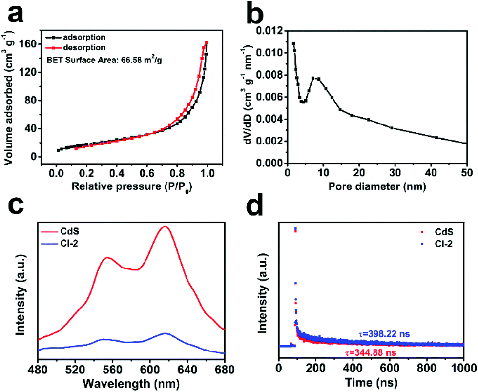 | ||
| Fig. 6 (a) Nitrogen adsorption–desorption isotherm and (b) pore size distribution of CdS/In2O3-2; (c) steady-state PL spectra and (d) PL decay spectra of CdS and CdS/In2O3–2. | ||
To analyze the reasons from the perspective of charge carrier separation, photoluminescence (PL) spectra of different photocatalysts were obtained. Compared with pure CdS, the weaker steady-state fluorescence intensity for CdS/In2O3-2 (shown in Fig. 6c) reveals that photo-generated electron–hole pairs are recombined with greater difficultly in the form of light radiation, indicating efficient charge separation in the heterostructures under excitation light.72,92 Moreover, the average PL lifetime calculated from PL decay spectra (Fig. 6d) is 398.22 ns for CdS/In2O3-2, longer than that of CdS (344.88 ns). Longer PL lifetimes mean slower kinetics of charge carrier recombination, which is undoubtedly in favour of the photocatalytic utilization of photo-generated carriers.40
Transient photocurrent and electrochemical impedance spectroscopy (EIS) measurements were carried out to provide more evidence for the enhanced photocatalytic activities of the CdS/In2O3 heterostructures. As illustrated in Fig. 7a, the photocurrent of CdS or In2O3 alone under the irradiation of a 300 W Xe lamp is rather small, while the photocurrent is dramatically increased for all CdS/In2O3 heterostructures. Such a difference indicates that in CdS/In2O3 heterostructures, the separation and transfer of the photo-induced carriers are much faster, which is in favour of the photocatalytic process without doubt.92 In addition, smaller semicircle diameters of EIS Nyquist plots for CdS/In2O3 heterostructures (Fig. 7b) suggest that CdS/In2O3 nanotubes with a lower charge transfer resistance are more beneficial to the transfer of charge carriers in photocatalysis.55,85 CdS/In2O3-2, which shows the highest photocurrent and the smallest semicircle diameter of EIS Nyquist plot, thus possesses the best photocatalytic activity, as shown in Fig. 5b.
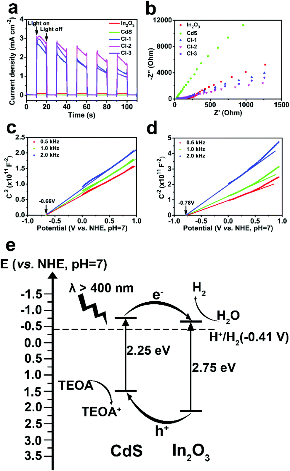 | ||
| Fig. 7 (a) Transient photocurrent responses and (b) EIS Nyquist plots of In2O3, CdS and CdS/In2O3 heterostructures; Mott-Schottky plots of (c) In2O3 nanotubes and (d) CdS nanoparticles; (e) schematic diagram of the band structure of CdS/In2O3 heterostructure. | ||
Mott-Schottky tests were further conducted to verify semiconductor types and obtain the flat band potential of In2O3 and CdS. In Mott-Schottky plots (Fig. 7c and d), the slope of the extension line of the straight-line portion is positive for In2O3 and CdS, revealing that both are n-type semiconductors.85,93 Furthermore, the flat band potentials are −0.66 and −0.78 V (vs. NHE, pH = 7) for In2O3 and CdS, respectively. It is reasonable to use the flat band potential of an n-type semiconductor to evaluate the reducing capacity of the electrons at the conduction band minimum (CBM).94,95 Both potentials are more negative than the reduction potential of H2O (−0.41 V vs. NHE, pH = 7), indicating that both In2O3 and CdS are potential catalysts for hydrogen production from H2O. Combined with Eg obtained from UV-vis DRS, the schematic diagram of the band structure of CdS/In2O3 heterostructure can be drawn (Fig. 7e). It is evident that CdS/In2O3 is a type-II heterostructure.49 Under visible light, In2O3 and CdS can generate electron–hole pairs which are then very likely to be separated efficiently through the staggered band structure. In other words, the photo-induced electrons are collected at the bottom of conduction band of In2O3, while the photo-induced holes are collected at the top of valence band of CdS. Intimate and extensive contact of In2O3 and CdS nanoparticles, described above, enlarges such an effect in a heterostructure. As a consequence, the recombination of photo-generated carriers is suppressed to a great extent, leading to the promotion of photocatalytic efficiency as more photo-induced charge carriers can transfer to the surface of photocatalysts to take part in the electrocatalytic process.
In summary, from the results of PL spectroscopy, transient photocurrent, electrochemical impedance spectroscopy as well as band structure analysis, we could deduce that the formation of a type-II heterostructure is the primary reason for the elevated photocatalytic activity of CdS/In2O3 heterostructures. What is more, the hollow and hierarchical tubular morphology composed of small In2O3 and CdS nanoparticles with intimate and extensive contact enlarges such an effect of heterostructure. As a result, separation and transfer of photo-generated carriers is tremendously improved in the heterostructures, leading to the huge enhancement of photocatalytic activity compared with pure In2O3 or CdS.
Photocatalytic stability test
Finally, the photocatalytic stability of CdS/In2O3-2 was also explored. It was verified that the activity of CdS/In2O3-2 remained relatively stable after being recycled 3 times (each one was as long as 4 h, seen in Fig. 8a). Besides, XRD and SEM analysis of CdS/In2O3-2 after the photocatalytic cyclic test did not show obvious changes (Fig. 8b and Fig. S16†), supporting the superior stability of such a heterostructure photocatalyst.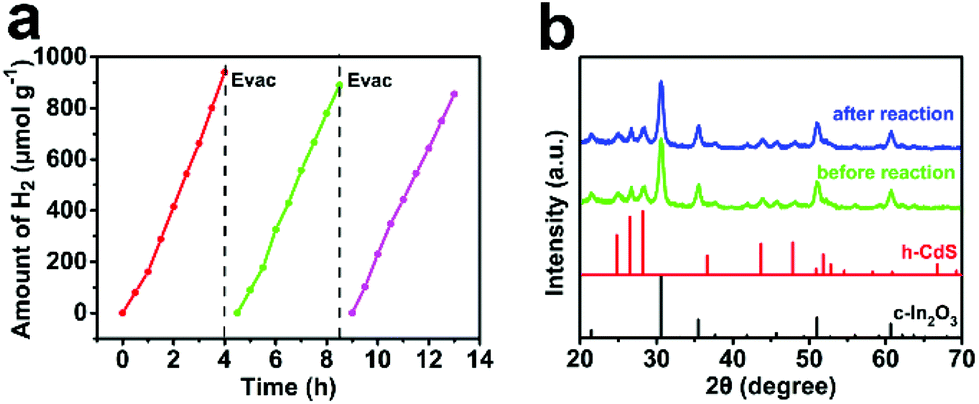 | ||
| Fig. 8 (a) Photocatalytic stability of CdS/In2O3-2 towards visible-light hydrogen production; (b) XRD patterns of CdS/In2O3-2 before and after the photocatalytic cyclic test. | ||
Conclusions
In summary, robust CdS/In2O3 hierarchical nanotubes were synthesized by a facile two-step method, that is, the formation of In2O3 hierarchical nanotubes by calcination of an In-MOF followed by in situ growth of CdS nanoparticles by a low-temperature oil bath method. The as-prepared CdS/In2O3 heterostructure is made up of small In2O3 and CdS nanoparticles with intimate and extensive contacts. Such a heterostructure not only ensures large interfaces between these two semiconductor components which are beneficial to the separation and transfer of photo-induced charge carriers through forming a type-II heterostructure, but also possesses advantages of hierarchical nanostructures, i.e., enhancing light absorption and increasing the number of catalytically-active sites. Therefore, the optimal CdS/In2O3-2 hierarchical nanotubes exhibited the best activity in visible-light photocatalytic hydrogen production without any cocatalysts, which was 78.6 times and 16.9 times greater than activities of In2O3 hierarchical nanotubes and CdS nanoparticles, respectively. This work not only explores the interfacial effect of In2O3 and CdS on visible-light photocatalytic hydrogen production without cocatalysts, but also provides a new idea for synthesizing highly-efficient sulfide/oxide heterostructure photocatalysts starting from MOFs, and for maximizing the interfacial effect of heterostructure photocatalysts on photocatalytic hydrogen evolution.Conflicts of interest
There are no conflicts to declare.Acknowledgements
This work was supported by the National Key Research and Development Program of China (No. 2016YFB0701100), the National Natural Science Foundation of China (No. 21832001, 21771009, 21573005, and 21621061), and the Beijing Natural Science Foundation (No. 2162019). We particularly appreciate the help of Qi Sun with electrochemical measurements including transient photocurrent, electrochemical impedance spectroscopy and Mott-Schottky tests.Notes and references
- P. L. Liao and E. A. Carter, Chem. Soc. Rev., 2013, 42, 2401–2422 RSC.
- W. G. Tu, Y. Zhou and Z. G. Zou, Adv. Mater., 2014, 26, 4607–4626 CrossRef CAS PubMed.
- D. Chen, X. G. Zhang and A. F. Lee, J. Mater. Chem. A, 2015, 3, 14487–14516 RSC.
- S. J. Xie, Q. H. Zhang, G. D. Liu and Y. Wang, Chem. Commun., 2016, 52, 35–59 RSC.
- X. X. Chang, T. Wang and J. L. Gong, Energy Environ. Sci., 2016, 9, 2177–2196 RSC.
- G. X. Zhao, X. B. Huang, X. X. Wang and X. K. Wang, J. Mater. Chem. A, 2017, 5, 21625–21649 RSC.
- J. Di, J. Xiong, H. M. Li and Z. Liu, Adv. Mater., 2018, 30, 1704548 CrossRef PubMed.
- N. Q. Wu, Nanoscale, 2018, 10, 2679–2696 RSC.
- X. Li, J. G. Yu and M. Jaroniec, Chem. Soc. Rev., 2016, 45, 2603–2636 RSC.
- J. W. Fu, J. G. Yu, C. J. Jiang and B. Cheng, Adv. Energy Mater., 2018, 8, 1701503 CrossRef.
- S. S. Chen, T. Takata and K. Domen, Nat. Rev. Mater., 2017, 2, 17050 CrossRef CAS.
- W. Y. Hu, W. Zhou, K. F. Zhang, X. C. Zhang, L. Wang, B. J. Jiang, G. H. Tian, D. Y. Zhao and H. G. Fu, J. Mater. Chem. A, 2016, 4, 7495–7502 RSC.
- X. N. Ren, Z. Y. Hu, J. Jin, L. Wu, C. Wang, J. Liu, F. Liu, M. Wu, Y. Li, G. Van Tendeloo and B. L. Su, ACS Appl. Mater. Interfaces, 2017, 9, 29687–29698 CrossRef CAS PubMed.
- X. L. Weng, Y. L. Zhang, F. Bi, F. Dong, Z. B. Wu and J. A. Darr, J. Mater. Chem. A, 2017, 5, 23766–23775 RSC.
- J. K. Zhang, Z. B. Yu, Z. Gao, H. B. Ge, S. C. Zhao, C. Q. Chen, S. Chen, X. L. Tong, M. H. Wang, Z. F. Zheng and Y. Qin, Angew. Chem., Int. Ed., 2017, 56, 816–820 CrossRef CAS PubMed.
- J. N. Hui, G. Zhang, C. S. Ni and J. T. S. Irvine, Chem. Commun., 2017, 53, 10038–10041 RSC.
- A. T. Garcia-Esparza, T. Shinagawa, S. Ould-Chikh, M. Qureshi, X. Y. Peng, N. N. Wei, D. H. Anjum, A. Clo, T. C. Weng, D. Nordlund, D. Sokaras, J. Kubota, K. Domen and K. Takanabe, Angew. Chem., Int. Ed., 2017, 56, 5780–5784 CrossRef CAS PubMed.
- Q. Wang, T. Hisatomi, Q. X. Jia, H. Tokudome, M. Zhong, C. Z. Wang, Z. H. Pan, T. Takata, M. Nakabayashi, N. Shibata, Y. B. Li, I. D. Sharp, A. Kudo, T. Yamada and K. Domen, Nat. Mater., 2016, 15, 611–615 CrossRef CAS PubMed.
- Y. J. Luo, X. M. Liu, X. H. Tang, Y. Luo, Q. Y. Zeng, X. L. Deng, S. L. Ding and Y. Q. Sun, J. Mater. Chem. A, 2014, 2, 14927–14939 RSC.
- M. Xiao, B. Luo, M. Q. Lyu, S. C. Wang and L. Z. Wang, Adv. Energy Mater., 2018, 8, 1701605 CrossRef.
- Y. L. Wang, T. Nie, Y. H. Li, X. L. Wang, L. R. Zheng, A. P. Chen, X. Q. Gong and H. G. Yang, Angew. Chem., Int. Ed., 2017, 56, 7430–7434 CrossRef CAS PubMed.
- Y. G. Chen, S. Zhao, X. Wang, Q. Peng, R. Lin, Y. Wang, R. A. Shen, X. Cao, L. B. Zhang, G. Zhou, J. Li, A. D. Xia and Y. D. Li, J. Am. Chem. Soc., 2016, 138, 4286–4289 CrossRef CAS PubMed.
- Q. C. Yuan, D. Liu, N. Zhang, W. Ye, H. X. Ju, L. Shi, R. Long, J. F. Zhu and Y. J. Xiong, Angew. Chem., Int. Ed., 2017, 56, 4206–4210 CrossRef CAS PubMed.
- L. Shang, B. Tong, H. J. Yu, G. I. N. Waterhouse, C. Zhou, Y. F. Zhao, M. Tahir, L. Z. Wu, C. H. Tung and T. R. Zhang, Adv. Energy Mater., 2016, 6, 1501241 CrossRef.
- G. X. Zhao, Y. B. Sun, W. Zhou, X. K. Wang, K. Chang, G. G. Liu, H. M. Liu, T. Kako and J. H. Ye, Adv. Mater., 2017, 29, 1703258 CrossRef PubMed.
- K. F. Wu, Z. Y. Chen, H. J. Lv, H. M. Zhu, C. L. Hill and T. Q. Lian, J. Am. Chem. Soc., 2014, 136, 7708–7716 CrossRef CAS PubMed.
- Y. Y. Zhang, L. L. Han, C. H. Wang, W. H. Wang, T. Ling, J. Yang, C. K. Dong, F. Lin and X. W. Du, ACS Catal., 2017, 7, 1470–1477 CrossRef CAS.
- H. M. Huang, B. Y. Dai, W. Wang, C. H. Lu, J. H. Kou, Y. R. Ni, L. Z. Wang and Z. Z. Xu, Nano Lett., 2017, 17, 3803–3808 CrossRef CAS PubMed.
- X. J. Sun, D. D. Yang, H. Dong, X. B. Meng, J. L. Sheng, X. Zhang, J. Z. Wei and F. M. Zhang, Sustainable Energy Fuels, 2018, 2, 1356–1361 RSC.
- J. S. Zhang, M. W. Zhang, R. Q. Sun and X. C. Wang, Angew. Chem., Int. Ed., 2012, 51, 10145–10149 CrossRef CAS PubMed.
- X. C. Wang, X. F. Chen, A. Thomas, X. Z. Fu and M. Antonietti, Adv. Mater., 2009, 21, 1609–1612 CrossRef CAS.
- G. G. Zhang, M. W. Zhang, X. X. Ye, X. Q. Qiu, S. Lin and X. C. Wang, Adv. Mater., 2014, 26, 805–809 CrossRef CAS PubMed.
- Y. J. Cui, Z. X. Ding, X. Z. Fu and X. C. Wang, Angew. Chem., Int. Ed., 2012, 51, 11814–11818 CrossRef CAS PubMed.
- J. S. Zhang, G. G. Zhang, X. F. Chen, S. Lin, L. Mçhlmann, G. Dołega, G. Lipner, M. Antonietti, S. Blechert and X. C. Wang, Angew. Chem., Int. Ed., 2012, 51, 3183–3187 CrossRef CAS PubMed.
- Z. Z. Lin and X. C. Wang, Angew. Chem., Int. Ed., 2013, 52, 1735–1738 CrossRef CAS PubMed.
- J. H. Sun, J. S. Zhang, M. W. Zhang, M. Antonietti, X. Z. Fu and X. C. Wang, Nat. Commun., 2012, 3, 1139 CrossRef.
- Y. Zhou, Z. P. Tian, Z. Y. Zhao, Q. Liu, J. H. Kou, X. Y. Chen, J. Gao, S. C. Yan and Z. G. Zou, ACS Appl. Mater. Interfaces, 2011, 3, 3594–3601 CrossRef CAS PubMed.
- X. X. Guo, X. Y. Qin, Z. J. Xue, C. B. Zhang, X. H. Sun, J. B. Hou and T. Wang, RSC Adv., 2016, 6, 48537–48542 RSC.
- Y. X. Pan, Y. You, S. Xin, Y. T. Li, G. T. Fu, Z. M. Cui, Y. L. Men, F. F. Cao, S. H. Yu and J. B. Goodenough, J. Am. Chem. Soc., 2017, 139, 4123–4129 CrossRef CAS PubMed.
- L. Liang, F. C. Lei, S. Gao, Y. F. Sun, X. C. Jiao, J. Wu, S. Qamar and Y. Xie, Angew. Chem., Int. Ed., 2015, 54, 13971–13974 CrossRef CAS PubMed.
- A. Etogo, R. Liu, J. B. Ren, L. W. Qi, C. C. Zheng, J. Q. Ning, Y. J. Zhong and Y. Hu, J. Mater. Chem. A, 2016, 4, 13242–13250 RSC.
- R. Jinnouchi, A. V. Akimov, S. Shirai, R. Asahi and O. V. Prezhdo, J. Phys. Chem. C, 2015, 119, 26925–26936 CrossRef CAS.
- P. Kwolek, K. Pilarczyk, T. Tokarski, K. Lewandowska and K. Szaciłowski, Nanoscale, 2014, 6, 2244–2254 RSC.
- W. J. Fang, Z. Jiang, L. Yu, H. Liu, W. F. Shangguan, C. Terashima and A. Fujishima, J. Catal., 2017, 352, 155–159 CrossRef CAS.
- H. Li, F. Qin, Z. P. Yang, X. M. Cui, J. F. Wang and L. Z. Zhang, J. Am. Chem. Soc., 2017, 139, 3513–3521 CrossRef CAS PubMed.
- D. W. Li, S. X. Ouyang, H. Xu, D. Lu, M. Zhao, X. L. Zhang and J. H. Ye, Chem. Commun., 2016, 52, 5989–5992 RSC.
- D. D. Zheng, X. N. Cao and X. C. Wang, Angew. Chem., Int. Ed., 2016, 55, 11512–11516 CrossRef CAS PubMed.
- Y. F. Xu, M. Z. Yang, B. X. Chen, X. D. Wang, H. Y. Chen, D. B. Kuang and C. Y. Su, J. Am. Chem. Soc., 2017, 139, 5660–5663 CrossRef CAS PubMed.
- J. X. Low, J. G. Yu, M. Jaroniec, S. Wageh and A. A. Al-Ghamdi, Adv. Mater., 2017, 29, 1601694 CrossRef PubMed.
- P. J. Yang, J. H. Zhao, J. Wang, B. Y. Cao, L. Li and Z. P. Zhu, J. Mater. Chem. A, 2015, 3, 8256–8259 RSC.
- J. H. Hu, L. J. Wang, P. Zhang, C. H. Liang and G. S. Shao, J. Power Sources, 2016, 328, 28–36 CrossRef CAS.
- L. J. Zhang, S. Li, B. K. Liu, D. J. Wang and T. F. Xie, ACS Catal., 2014, 4, 3724–3729 CrossRef CAS.
- X. Yang, J. Xu, T. L. Wong, Q. D. Yang and C. S. Lee, Phys. Chem. Chem. Phys., 2013, 15, 12688–12693 RSC.
- W. Y. Wang, X. W. Wang, C. X. Zhou, B. Du, J. X. Cai, G. Feng and R. B. Zhang, J. Phys. Chem. C, 2017, 121, 19104–19111 CrossRef CAS.
- S. B. Wang, B. Y. Guan and X. W. Lou, J. Am. Chem. Soc., 2018, 140, 5037–5040 CrossRef CAS PubMed.
- M. Lan, R. M. Guo, Y. B. Dou, J. Zhou, A. W. Zhou and J. R. Li, Nano Energy, 2017, 33, 238–246 CrossRef CAS.
- K. E. deKrafft, C. Wang and W. B. Lin, Adv. Mater., 2012, 24, 2014–2018 CrossRef CAS PubMed.
- H. R. Chen, K. Shen, J. Y. Chen, X. D. Chen and Y. W. Li, J. Mater. Chem. A, 2017, 5, 9937–9945 RSC.
- Z. F. Huang, J. J. Song, K. Li, M. Tahir, Y. T. Wang, L. Pan, L. Wang, X. W. Zhang and J. J. Zou, J. Am. Chem. Soc., 2016, 138, 1359–1365 CrossRef CAS PubMed.
- J. M. Chen, J. Y. Chen and Y. W. Li, J. Mater. Chem. A, 2017, 5, 24116–24125 RSC.
- S. B. Wang, B. Y. Guan, Y. Lu and X. W. Lou, J. Am. Chem. Soc., 2017, 139, 17305–17308 CrossRef CAS PubMed.
- X. X. Zhao, J. R. Feng, J. Liu, W. Shi, G. M. Yang, G. C. Wang and P. Cheng, Angew. Chem., Int. Ed., 2018, 57, 9790–9794 CrossRef CAS PubMed.
- L. He, T. E. Wood, B. Wu, Y. C. Dong, L. B. Hoch, L. M. Reyes, D. Wang, C. Kübel, C. X. Qian, J. Jia, K. Liao, P. G. O'Brien, A. Sandhel, J. Y. Y. Loh, P. Szymanski, N. P. Kherani, T. C. Sum, C. A. Mims and G. A. Ozin, ACS Nano, 2016, 10, 5578–5586 CrossRef CAS PubMed.
- B. L. Tao, Y. Zhang, D. Z. Han, Y. P. Li and Z. F. Yan, J. Mater. Chem. A, 2014, 2, 5455–5461 RSC.
- H. Huang, Z. K. Yue, G. Li, X. M. Wang, J. Huang, Y. K. Du and P. Yang, J. Mater. Chem. A, 2014, 2, 20118–20125 RSC.
- D. F. Wang, Z. G. Zou and J. H. Ye, Chem. Mater., 2005, 17, 3255–3261 CrossRef CAS.
- A. Nashim, S. Martha and K. M. Parida, ChemCatChem, 2013, 5, 2352–2359 CrossRef CAS.
- S. J. Hu, B. Chi, J. Pu and L. Jian, J. Mater. Chem. A, 2014, 2, 19260–19267 RSC.
- S. Martha, K. H. Reddy and K. M. Parida, J. Mater. Chem. A, 2014, 2, 3621–3631 RSC.
- S. W. Cao, X. F. Liu, Y. P. Yuan, Z. Y. Zhang, Y. S. Liao, J. Fang, S. C. J. Loo, T. C. Sum and C. Xue, Appl. Catal., B, 2014, 147, 940–946 CrossRef CAS.
- D. D. Ma, J. W. Shi, Y. J. Zou, Z. Y. Fan, J. W. Shi, L. H. Cheng, D. K. Sun, Z. Y. Wang and C. M. Niu, Nanoscale, 2018, 10, 7860–7870 RSC.
- B. C. Qiu, Q. H. Zhu, M. M. Du, L. G. Fan, M. Y. Xing and J. L. Zhang, Angew. Chem., Int. Ed., 2017, 56, 2684–2688 CrossRef CAS PubMed.
- J. R. Ran, X. L. Wang, B. C. Zhu and S. Z. Qiao, Chem. Commun., 2017, 53, 9882–9885 RSC.
- K. Li, M. Han, R. Chen, S. L. Li, S. L. Xie, C. Y. Mao, X. H. Bu, X. L. Cao, L. Z. Dong, P. Y. Feng and Y. Q. Lan, Adv. Mater., 2016, 28, 8906–8911 CrossRef CAS PubMed.
- Z. Fang, J. J. Zhou, Y. M. Sun, J. H. Hu, L. Liang, R. Xu and H. W. Duan, Nanoscale, 2017, 9, 17794–17801 RSC.
- J. Feng, C. H. An, L. X. Dai, J. X. Liu, G. J. Wei, S. Bai, J. Zhang and Y. J. Xiong, Chem. Eng. J., 2016, 283, 351–357 CrossRef CAS.
- Q. M. Sun, N. Wang, J. H. Yu and J. C. Yu, Adv. Mater., 2018, 1804368 CrossRef PubMed.
- T. Simon, N. Bouchonville, M. J. Berr, A. Vaneski, A. Adrovic, D. Volbers, R. Wyrwich, M. Döblinger, A. S. Susha, A. L. Rogach, F. Jäckel, J. K. Stolarczyk and J. Feldmann, Nat. Mater., 2014, 13, 1013–1018 CrossRef CAS PubMed.
- L. Yuan, C. Han, M. Q. Yang and Y. J. Xu, Int. Rev. Phys. Chem., 2016, 35, 1–36 Search PubMed.
- Z. R. Tang, B. Han, C. Han and Y. J. Xu, J. Mater. Chem. A, 2017, 5, 2387–2410 RSC.
- M. Q. Yang, C. Han and Y. J. Xu, J. Phys. Chem. C, 2015, 119, 27234–27246 CrossRef CAS.
- B. Han, S. Q. Liu, N. Zhang, Y. J. Xu and Z. R. Tang, Appl. Catal., B, 2017, 202, 298–304 CrossRef CAS.
- Y. X. Pan, H. Q. Zhuang, J. D. Hong, Z. Fang, H. Liu, B. Liu, Y. Z. Huang and R. Xu, ChemSusChem, 2014, 7, 2537–2544 CrossRef CAS PubMed.
- W. Cho, H. J. Lee and M. Oh, J. Am. Chem. Soc., 2008, 130, 16943–16946 CrossRef CAS PubMed.
- M. Y. Ye, Z. H. Zhao, Z. F. Hu, L. Q. Liu, H. M. Ji, Z. R. Shen and T. Y. Ma, Angew. Chem., Int. Ed., 2017, 56, 8407–8411 CrossRef CAS PubMed.
- X. F. Li, C. Q. Wang, B. Li, Y. Shao and D. Z. Li, Phys. Chem. Chem. Phys., 2016, 18, 27848–27857 RSC.
- Y. T. Xiao, G. H. Tian, Y. J. Chen, X. Zhang, H. Y. Fu and H. G. Fu, Appl. Catal., B, 2018, 225, 477–486 CrossRef CAS.
- F. Zhang, X. Y. Li, Q. D. Zhao and D. K. Zhang, ACS Sustainable Chem. Eng., 2016, 4, 4554–4562 CrossRef CAS.
- V. Amoli, M. G. Sibi, B. Banerjee, M. Anand, A. Maurya, S. A. Farooqui, A. Bhaumik and A. K. Sinha, ACS Appl. Mater. Interfaces, 2015, 7, 810–822 CrossRef CAS PubMed.
- Z. Wang, W. W. Wu, Q. Xu, G. D. Li, S. H. Liu, X. F. Jia, Y. Qin and Z. L. Wang, Nano Energy, 2017, 38, 518–525 CrossRef CAS.
- J. Z. Chen, X. J. Wu, L. S. Yin, B. Li, X. Hong, Z. X. Fan, B. Chen, C. Xue and H. Zhang, Angew. Chem., Int. Ed., 2015, 54, 1210–1214 CrossRef CAS PubMed.
- S. Y. Bao, Q. F. Wu, S. Z. Chang, B. Z. Tian and J. L. Zhang, Catal. Sci. Technol., 2017, 7, 124–132 RSC.
- Z. W. Tong, D. Yang, Z. Li, Y. H. Nan, F. Ding, Y. C. Shen and Z. Y. Jiang, ACS Nano, 2017, 11, 1103–1112 CrossRef CAS.
- S. N. Talapaneni, G. P. Mane, D. H. Park, K. S. Lakhi, K. Ramadass, S. Joseph, W. M. Skinner, U. Ravon, K. Al-Bahily and A. Vinu, J. Mater. Chem. A, 2017, 5, 18183–18192 RSC.
- N. Srinivasan, E. Sakai and M. Miyauchi, ACS Catal., 2016, 6, 2197–2200 CrossRef CAS.
Footnote |
| † Electronic supplementary information (ESI) available: More XRD patterns, SEM images, zeta potential, TEM images, XPS spectrum, Tauc plots, nitrogen adsorption–desorption isotherms and photocatalytic activity tests. See DOI: 10.1039/c8qi01202d |
| This journal is © the Partner Organisations 2019 |