DOI:
10.1039/C9NH00460B
(Communication)
Nanoscale Horiz., 2020,
5, 57-64
Engineering spin and antiferromagnetic resonances to realize an efficient direction-multiplexed visible meta-hologram†
Received
11th July 2019
, Accepted 7th August 2019
First published on 7th August 2019
Abstract
Driven by the need for enhanced integrated performance and rapid development of ultrathin multitasked optical devices, this paper experimentally demonstrates monolayer direction-controlled multiplexing of a transmissive meta-hologram in the visible domain. The directional sensitivity is designed by imparting direction-controlled spin-dependent holographic recordings in the monolayer structure. The designed metasurface hologram consists of nano half-waveplates (HWPs) of low loss hydrogenated amorphous silicon (a-Si:H). These nano-featured HWPs are carefully designed and optimized for circularly polarized (CP) illumination to not only excite electric and magnetic resonances simultaneously but also to excite antiferromagnetic modes to ensure high transmission for the cross CP-light. The antiferromagnetic modes are excited in such a way that the transmitted CP-light maintains the Ex component of the incident CP-light through even antiparallel magnetic dipoles while they reverse the Ey component via odd antiparallel magnetic dipoles. As compared to the standard amorphous silicon, our a-Si:H exhibits a much lower absorption coefficient in the visible domain. The proposed single-layer design is an advanced step towards scalability, low-cost fabrication, and on-chip implementation of novel metasurfaces with substantially higher performance in the visible domain.
New concepts
Metasurfaces have provided a planar and superficial solution to manipulating the intensity, polarization and phase of incident electromagnetic wavefronts. Here, we have demonstrated a new approach to multiplex two distinct pieces of information onto a monolayer metasurface hologram operating in the forward and backward directions depending upon the direction of light incident on the device. Particularly, this paper describes in detail the electric/magnetic resonances and the antiferromagnetic modes phenomenon occurring inside of hydrogenated amorphous silicon (a-Si:H) metasurfaces, which are the major factors for obtaining high transmission efficiency. Our proposed a-Si:H-based direction-multiplexing meta-hologram not only performs better than previously reported metasurfaces based on standard a-Si in terms of efficiency and image contrast but also outweighs three-dimensional and multi-layer asymmetric structures in terms of design simplicity and manufactural ease. Generation of multiplexed high-quality holographic images with high efficiency (or high transmission) and a facile CMOS compatible fabrication approach reinforces the ability of the proposed metasurface to be employed in multi-functional photonic and optical devices such as ultrathin holographic movie displays and anti-counterfeiting holographic displays.
|
1. Introduction
Computer-generated holography (CGH) involves iterative numerical algorithms to obtain the phase and/or amplitude profiles needed to physically realize holograms.1–4 Metasurfaces consist of arrays of subwavelength nanoresonators that can control the wavefront of light in the desired way.5–8 They recently proved themselves to be an effective platform for CGH by surpassing the quality of traditional holograms. These metasurface holograms showed prospects not only in imaging and displays9–14 but also in security.15 Metasurface holography was mostly realized using plasmonic structures, both in the transmission16,17 and reflection modes.18,19 Li et al. have demonstrated a multicolor plasmonic metahologram that can produce three distinct RGB images depending upon the angles of incident lights, i.e., red, green, and blue. The off-axis holographic images are generated with optimal incident angles to reduce the crosstalk in the area of observation.20 A plasmonic catenary aperture array-based metasurface operating in an ultra-broadband regime is also presented to achieve achromatic performance. It is theoretically and experimentally demonstrated that these spatially continuous structures possess a spectrally achromatic phase distribution.21 However, plasmonic metasurfaces consisting of metallic nanoantennas suffer from severe Ohmic losses and, hence, limit the theoretical efficiency to only 25% in transmission mode.22 The efficiency turns out to be even lower for the experimental realization due to fabrication imperfections etc. This opens the hunt for a suitable material-platform for realizing highly efficient transmission mode metasurfaces.
The rigorous investigations revealed that high refractive index dielectrics could be an ideal candidate for this purpose.23–26 The respective dielectric metasurfaces demonstrated both electric and magnetic dipole resonances in the region of interest,24 succeeding their plasmonic counterparts in efficiency and, hence, offering a better platform for realizing transmission type metasurface holograms. Yang et al. employed poly-Si based nanoresonators to design a metasurface.27 The dimensions of the nanostructures were tailored to achieve the required phase shift and maximize the cross-polarized reflection at the operational range of the wavelength (λ = 1367 to 1380 nm). Zhou et al. reported an efficient metasurface (47%) using crystalline Si (c-Si) nanopillars with a full phase control (of 0–2π) at a wavelength of 532 nm.28 Amorphous silicon (a-Si) has also been used for producing metasurface holograms because it can be easily deposited on substrates of any kind.29 However, significant dielectric losses of a-Si are observed in the visible domain (as shown in Fig. S1, ESI†![[thin space (1/6-em)]](https://www.rsc.org/images/entities/char_2009.gif) 30), which seriously deteriorates the efficiency and image fidelity. Dielectric platforms such as TiO2 and GaN share high refractive index with transparency at visible frequencies. The ellipsometry data of TiO231 and GaN32 (Fig. S1, ESI†) advocate their utility for materializing highly efficient metaholograms,9 metalenses33,34 and optical vortex generators.35 The main drawbacks of these two dielectric platforms are their incompatibility with the existing CMOS industry and the required large height to width ratios (up to ∼15).9,33,36 To overcome these drawbacks, we propose processing of a-Si via controlled deposition. The extinction coefficient of a-Si can be reduced over a broadband frequency range by the inclusion of hydrogen, passivating the unsaturated bonds and therefore eliminating the gap states.37 As a result, hydrogenated a-Si (a-Si:H) provides a higher refractive index relative to TiO2 and GaN and comparably low-enough extinction coefficient, as depicted by our measured ellipsometry data of a-Si:H in Fig. S1 (ESI†). This dielectric platform provides a CMOS-compatible solution for realizing various highly efficient optical elements scalably and cost effectively.
30), which seriously deteriorates the efficiency and image fidelity. Dielectric platforms such as TiO2 and GaN share high refractive index with transparency at visible frequencies. The ellipsometry data of TiO231 and GaN32 (Fig. S1, ESI†) advocate their utility for materializing highly efficient metaholograms,9 metalenses33,34 and optical vortex generators.35 The main drawbacks of these two dielectric platforms are their incompatibility with the existing CMOS industry and the required large height to width ratios (up to ∼15).9,33,36 To overcome these drawbacks, we propose processing of a-Si via controlled deposition. The extinction coefficient of a-Si can be reduced over a broadband frequency range by the inclusion of hydrogen, passivating the unsaturated bonds and therefore eliminating the gap states.37 As a result, hydrogenated a-Si (a-Si:H) provides a higher refractive index relative to TiO2 and GaN and comparably low-enough extinction coefficient, as depicted by our measured ellipsometry data of a-Si:H in Fig. S1 (ESI†). This dielectric platform provides a CMOS-compatible solution for realizing various highly efficient optical elements scalably and cost effectively.
In addition, metamaterials/metasurfaces possess a great potential to effectuate the requirements of device scalability and integration for multiple applications in the field of optics. Most of these developments are culminated in a single type of operation, e.g., single facial or half space operation.38–40 In contrast, metamaterials/metasurfaces that are designed to attain asymmetric transmission (AT) can provide an alternative route to realize full face, bifacial and bifunctional metadevices.41–45 The underlying physical mechanism that governs the AT is known as optical chirality. According to the optical chirality of a planar medium, there exists a difference between the transmission of cross-polarized components under a specific polarization of incidence in the forward and backward directions.45 Initially optical chirality was achieved through a single device using multilayer metamaterials.41,47 Such structures were susceptible to difficult and time-consuming fabrication methods to incorporate accurate alignment admitting subsidiary layers. A bilayer and bidirectional metasurface based polarizer was proposed by Chen et al. using stepped slit grove nanoelements to perform different operations in different directions. The maximum working efficiencies of the metadevice were 15.5% and 17% in the forward and backward directions, respectively, at the operation wavelength of 735 nm.48
The first monolayer metasurface based on asymmetric spin orbit interactions exhibiting AT more than four times greater than the previously reported monolayer metasurfaces was demonstrated by Zhang et al.49 Along with multiple novel functionalities there comes a great deal of complexity in the design (i.e., these metamaterials/metasurfaces possess nanoelements with large dimensions49 or a supplementary layered structure, to gain an extra degree of freedom43,48). The complex design and fabrication make numerical simulations more computationally expensive and limit the scaling down of the bidirectional scheme to operate in the visible domain.48–50
Here we employ a novel approach using a monolayer all-dielectric metasurface to vindicate the pragmatic features, namely, the operation of the metasurface hologram in the forward and backward directions with unique information at each face. We have exploited the symmetry of the conversion of circularly polarized light into the cross-polarized component for propagation in opposite directions using similar rectangular nanoelements with two types of orientation angle shifts. The first shift is required to achieve full phase coverage. The second shift is needed to add the extra degree of direction multiplexing. In the case of incident light with circular polarization in the forward direction, our metasurface produces an image of the Information Technology University's logo “ITU” at the front face as shown in Fig. 3e. The same metasurface produces an image of the RHO laboratory's logo “RHO” at the rear face when illuminated from the backward direction as represented in Fig. 3f. The definitions of the forward and backward directions are relative to the origin of light illumination with respect to the metasurface vector M as shown in Fig. 3e and 3f. The hologram is designed to operate at the 633 nm wavelength. This direction-multiplexed hologram is shown to demonstrate high image fidelity and high transmission efficiency.
2. Results and discussion
Design and methodologies for the direction-multiplexed metahologram
A high refractive indexed nanoelement, depending on its geometry, has the localized effect of changing the phase and wavefront of the incident light. A rectangular nanoelement can act as a half-waveplate (HWP). Therefore, we can utilize an array of these nanoelements to construct a metasurface hologram.12 This enables us to introduce a spatially dependent change in the phase at the interface. In comparison with TiO29 and GaN,33,36 the required phase coverage (0–2π) is achieved at a much lower aspect ratio (4.7) in a-Si:H with the nanoelement height of 380 nm, hence, vindicating its greater manufactural ease. To ensure the maximum transmission efficiency of the cross-polarized component, the structural parameters of the unit element (i.e., periodicity (U), length (l) and width (t)) are optimized. The largest periodicity of the nanoelement is limited by the Nyquist criterion of sampling (U < λ/2NA). With an initial guess of length and width, the optimum periodicity was found to be 290 nm as shown in Fig. 1a. In the next step, the numerical simulations for total transmission (Ttot), cross-polarized (Tcross) and co-polarized (Tco) efficiencies are performed by sweeping the length and width of the nanoelement as shown in Fig. 1b–d respectively. The white dashed curve in Fig. 1c depicts the region of maximum cross-polarized efficiency. It is evident from Fig. 1b–d that the selection of length and width (indicated by white stars) is made based on the maximum cross-polarized efficiency, minimum co-polarized efficiency and manufactural ease.
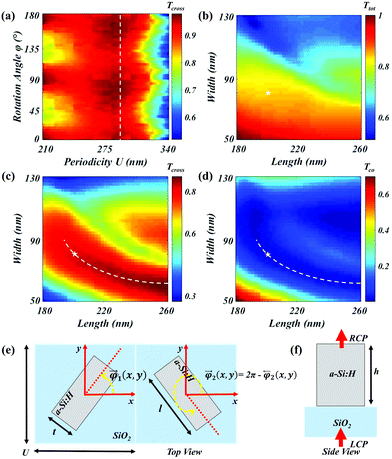 |
| | Fig. 1 Numerical optimization of the a-Si:H unit element. (a) Cross-polarized efficiency (Tcross) for various rotation angles (φ) and periodicities (U) of the a-Si:H unit element. The white dashed line is drawn at U = 290 nm, showing the maximum average value (0.97) of Tcross. (b) Total transmission efficiency (Ttot), (c) the Tcross and (d) co-polarized efficiency (Tco) for various widths (t) and lengths (l). The white dashed curve in (c) indicates the region of interest having the maximum values of Tcross and minimum values of Tco. Moreover, the white star indicates the selection of t (80 nm) and l (200 nm). (e) Schematic of the supercell containing two unit elements of a-Si:H on a quartz substrate. Two different rotation angles are imparted on a-Si:H nanoelements to attain the required phase difference for direction multiplexing. The top view in (e) and the side view in (f) indicate the optimized values of t, l, h and U under the illumination by red (633 nm) light with left circular polarization (LCP). | |
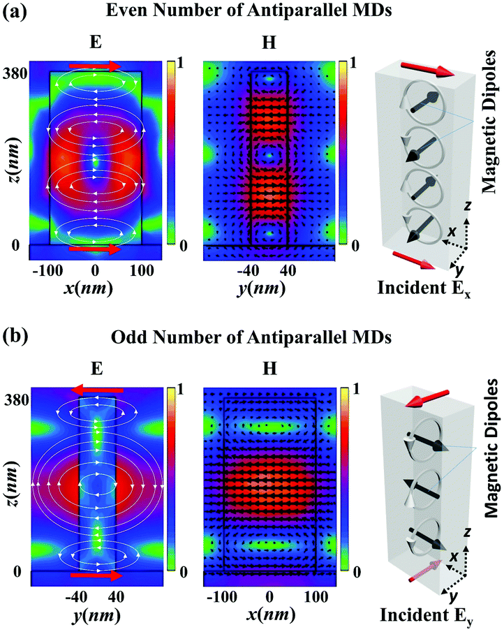
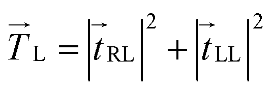
The use of antiferromagnetic resonance modes has been reported in multi-layered magnetic structures for information storage applications.51 Recently, these resonance modes are investigated in artificially engineered nanostructures such as silicon nanoelements with larger aspect ratios52 and hybrid metamolecules.53 Here, the behavior of dielectric antiferromagnetic resonance modes in an optimal a-Si:H nanoelement are investigated to underpin the physical mechanism behind the high transmission and the phase delay of 180° amidst orthogonal electric field components which is necessary to achieve polarization conversion. The electric displacement currents (DCs) in the a-Si:H nanoelement induce the magnetic fields which are responsible for the electromagnetic resonances. The confinement of both magnetic and electric resonance modes in the nanoelement under x- and y-polarizations hold promise for the high transmission for the operation wavelength of 633 nm, as shown in Fig. 2a and b. Therefore, the a-Si:H nanoelement is designed to excite antiferromagnetic resonance modes with a series of antiparallel magnetic dipoles (MDs) and electric DCs. Theses multiple antiparallel MD modes are originated from the combination of Mie resonances and Fabry–Perot modes, also known as hybrid Mie–Fabry–Perot modes.52 Moreover, the constructive interference of these antiparallel MD modes and induced electric DCs leads to a novel type of optical magnetism similar to the vertically aligned assembly of spins in the antiferromagnetic materials.54 In the case of x-polarized incidence, the magnetic field has four antiparallel MDs located along the propagation direction inside the nanoelement, as shown in Fig. 2a. Moreover, the induced electric field has four electric DCs inside the nanoelement with alternate directions i.e., clockwise and anti-clockwise. The even number of induced electric DCs align input (bottom) and output (top) electric field vectors in the same direction, as shown in Fig. 2a. In the case of y-polarized incidence, the antiferromagnetic resonance mode has three antiparallel MDs and electric DCs. The odd number of electric DCs enforces the electric field vector of the output light to have opposite direction compared to the input electric field vector as shown in Fig. 2b. This implies that the x (y) component of circularly polarized light is retained (inversed) after passing through the a-Si:H nanoelement. Thus, enabling a phase delay of 180° that is required to achieve high efficiency of orthogonal polarization conversion. The proposed a-Si:H based unit cell has higher transmission efficiency and conversion efficiency (75 and 74% respectively) at the operational wavelength than the previously reported a-Si-based design.29 The conversion efficiency (from left circular polarization (LCP) to right circular polarization (RCP) or RCP to LCP) is defined as the ratio of the cross-polarized light power to the incident light power. This optimization also ensures the desired phase coverage (0–2π).
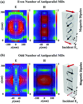 |
| | Fig. 2 Dielectric antiferromagnetic resonances in the optimal a-Si:H nanoelement. Absolute electric (E) and magnetic (H) cross-sectional fields (V m−1 and A m−1) in an a-Si:H nanoelement (black rectangles) under (a) x-polarized and (b) y-polarized light illumination, respectively. The antiferromagnetic resonance modes are excited in the a-Si:H nanoelement with even and odd vertical antiparallel MDs and circular electric DCs. The induced electric and magnetic field vectors are depicted in white lines and black arrows, respectively. Both antiferromagnetic modes are confined in the nanoelement at a wavelength of 633 nm. Red arrows at the bottom and top sides of the nanoelement show the direction of the incident and transmitted electric field vectors, respectively. The long axis of the nanoelement is parallel to the x-axis. | |
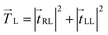
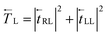
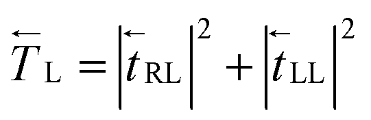
For simplicity of the design, we exploit the symmetry of the conversion of circularly polarized light into a cross-polarized component for propagation in opposite directions using rectangular nanoelements. This method provides us with an extra degree of freedom and control over the scattered wave. The total transmission for incident light with LCP in the forward and backward directions (eqn (1) and (2) respectively) can be expressed as follows:46
| |
 | (1) |
| |
 | (2) |
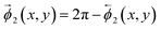
The first and second terms in both equations represent cross-polarized and co-polarized components of the transmitted light, respectively. Due to the symmetric nature of nanoelements, the cross-polarized transmission components are the same for both directions  . The phase difference (ΔΦ) between two nanoelements (Fig. 1e) at the interface can be engineered to incorporate distinct information in the forward and backward directions, which is governed by the following equations:
| |
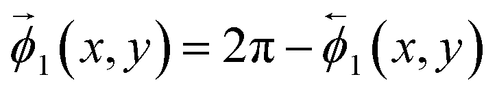
ΔΦ = 2σ(![[small phi, Greek, vector]](https://www.rsc.org/images/entities/i_char_e13a.gif) 1(x,y) − 2(x,y)) 1(x,y) − 2(x,y))
| (3) |
| |
 | (4) |
| |
 | (5) |
where
1(
x,
y) and

are the rotation angles associated with first nanoelements in the supercell for the forward and backward directions, respectively. Similarly,
2(
x,
y) and

denote the rotation angles of the second nanoelement in the supercell for the forward and backward directions, respectively as shown in
Fig. 1e. Moreover,
1(
x,
y) and

correspond to the desired phase maps of two distinct images. The value of
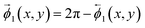
σ is either +1 or −1 depending on the helicity of the incident light (with LCP or RCP respectively). In the case of incident light with LCP, the expressions of the total electric fields transmitted from a supercell (
Fig. 1e) containing two nanoelements with shifted rotation angles are derived in the supplementary information and given by
| |
 | (6) |
| |
 | (7) |
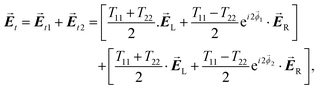
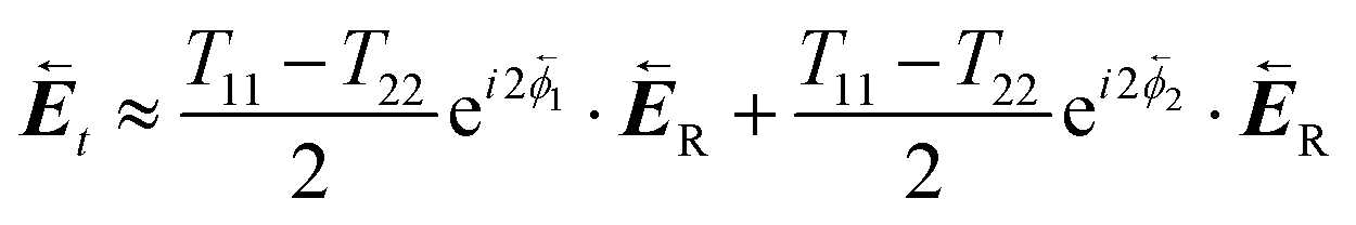
The bold letters indicate vector quantities; however, the top arrows only correspond to the direction i.e., forward or backward. Et1 and Et2 are the electric fields scattered from the first and second nanoelements in the supercell, respectively. T11 and T22 denote the complex transmission coefficients of the a-Si:H nanoelement when the polarization of illumination is parallel to the long and short axes of the nanoelement, respectively. According to eqn (6) and (7), the phase of the cross-polarized component depicts linear dependency on the rotation angle of the nanoelement with a factor of 2. Numerical optimization and simulations (explained previously) not only verified the linear dependency but also ensured the maximum value of the cross-polarized component. Therefore, the co-polarized components of the transmitted electric fields (1st and 3rd terms) are small and can be neglected.
| |
 | (8) |
| |
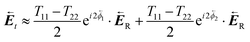 | (9) |
Hence, the total electric field transmitted from a supercell in the forward or backward direction is mainly composed of two cross-polarized components carrying Pancharatnam–Berry phases as expressed in eqn (8) and (9). If the phase difference amidst nanoelements in a supercell (ΔΦ) is rightly imparted, the inherent symmetry of the phase has a practical consequence: a phase converging in the forward direction, for example, will operate as a diverging lens in the backward direction and vice versa. The phase maps and the rotation angle profiles of these images can be calculated via the iterative Fourier transform method (IFTM).3,4
The metasurface hologram employing the phase profile associated with 1(x,y) can produce an image upon LCP illumination along the direction of vector M (forward direction) as shown in Fig. 3a. The same metasurface can diverge the transmitted light upon LCP illumination along the direction of the −M vector (backward direction) and, hence, will produce no information as shown in Fig. 3b. The second metasurface containing nanoelements with different phase profiles associated with  can produce a different image in the backward direction (Fig. 3d) and no image in the forward direction (Fig. 3c). Finally, both metasurface holograms are combined to reproduce distinct holographic images on the observation plane depending on the direction of the incident light, as shown in Fig. 3e and f.
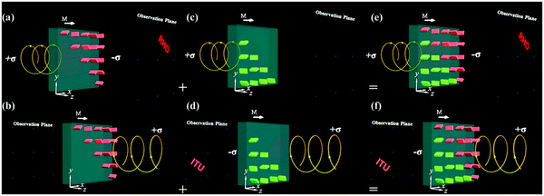 |
| | Fig. 3 Generation of the direction-multiplexed metasurface hologram. A metasurface (with (x,y)) operating in (a) the forward direction producing an image of the RHO Laboratory's logo “RHO”. (b) The same metasurface producing no image in the backward direction. The second metasurface (with  ) diverging the scattered light in (c) the forward direction and producing the desired logo of Information Technology University “ITU” in (d) the backward direction. (e) Reproduction of the holographic image of logo “RHO” in the forward direction and (f) the holographic image of logo “ITU” in the backward direction by multiplexing two distinct metasurfaces for dual operation. At transmission sides, the diverging beam is depicted in green color and the beam containing information about the holographic images is represented in red color. Two distinct phase maps of images with logos “RHO” and “ITU” are obtained using the iterative Fourier transform method. The phase maps of these two images are compensated for the off-axis projection of holographic images. In conjunction with that, both phase maps are also modified to maintain the required phase shift for direction-multiplexing (eqn (3)). These phase maps are then combined to form the 1378 × 1378 elements matrix. This corresponds to a metasurface with a size equal to 399.62 μm2. The phase maps are combined such that the top-right half of the metasurface corresponds to the holographic image “RHO” for the forward direction and the bottom-left half is associated with the holographic image “ITU” for the backward direction. ) diverging the scattered light in (c) the forward direction and producing the desired logo of Information Technology University “ITU” in (d) the backward direction. (e) Reproduction of the holographic image of logo “RHO” in the forward direction and (f) the holographic image of logo “ITU” in the backward direction by multiplexing two distinct metasurfaces for dual operation. At transmission sides, the diverging beam is depicted in green color and the beam containing information about the holographic images is represented in red color. Two distinct phase maps of images with logos “RHO” and “ITU” are obtained using the iterative Fourier transform method. The phase maps of these two images are compensated for the off-axis projection of holographic images. In conjunction with that, both phase maps are also modified to maintain the required phase shift for direction-multiplexing (eqn (3)). These phase maps are then combined to form the 1378 × 1378 elements matrix. This corresponds to a metasurface with a size equal to 399.62 μm2. The phase maps are combined such that the top-right half of the metasurface corresponds to the holographic image “RHO” for the forward direction and the bottom-left half is associated with the holographic image “ITU” for the backward direction. | |
Experimental verification of the direction-multiplexed metahologram
Using the IFTM, phase matrices containing 1378 × 1378 elements are calculated for each image (“RHO” and “ITU”) separately and then multiplexed together in such a way that both share the phase difference with each other given in eqn (3). Initially for the proof of concept, the rotation angles associated with the multiplexed phase profile are encoded onto a single 40.02 × 40.02 μm2 metasurface with a displacement of 290 nm using commercially available finite difference time domain (FDTD) software (Lumerical). Perfectly matched layer (PML) boundary conditions are used during these simulations. The optical outputs of simulation that illustrate the direction-multiplexed metasurface hologram concept are shown in Fig. 4a and b. To fabricate the 399.62 μm2 direction-multiplexed metasurface hologram, a 380 nm thick a-Si:H layer is deposited on top of a 500 μm thick quartz (SiO2) substrate via PECVD. The rate of this deposition is kept at 1.3 nm s−1. Hydrogen (H2) and saline (SiH4) gasses are used during the deposition with flow rates equal to 75 and 10 sccm respectively. Rectangular a-Si:H nanoelements are defined by E-beam lithography using a positive photoresist. This is followed by the deposition of a 30 nm chromium layer and the lift-off process. After dry etching via a chromium etch mask, geometrical structures are translated onto the a-Si:H. More details of the fabrication methodology can be found in Section S3 in the ESI,† and the scanning electron microscope images of the fabricated direction-multiplexed metasurface hologram are shown in the ESI,† Fig. S2.
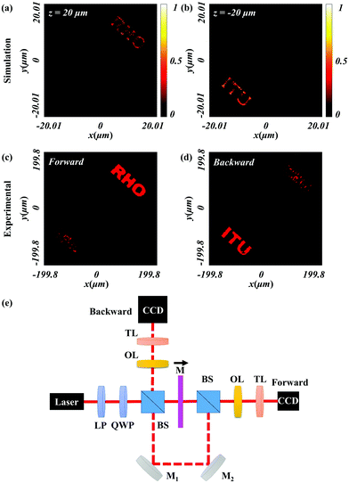 |
| | Fig. 4 Fresnel-type hologram illustration via a direction-multiplexed metasurface. FDTD simulations showing the amplitude profile of the hologram under LCP incident light operating in (a) the forward and (b) backward directions. Measured images captured using a CCD camera in (c) the forward and (d) backward directions. The size of the metasurface during simulation is 40.02 μm2, while the size of the fabricated metasurface is 399.62 μm2. (e) Optical characterization setup for the measurement of an amplitude profile. A HeNe laser light at a wavelength of 633 nm is used. A linear polarizer (LP) along with a quarter wave plate (QWP) covert the light into LCP. The LCP light is split by a 50/50 beam splitter (BS). A portion of light passes through the metasurface sample along the direction of vector M and produces a holographic image (logo of “RHO”) in the forward direction. When the silver mirrors (M1 and M2) are activated, the second portion of light (dashed line) is reflected through M1 and M2. Another BS is used to allow the light to enter from the opposite face of the metasurface such that the light is anti-parallel to vector M. The second holographic image (log of “ITU”) is produced in the backward direction. The images are captured using a CCD camera with an objective lens (OL) and tube lens (TL) through z-position adjustment of the metasurface sample. | |
A modified microscopic characterization setup is built to observe the holographic images on both faces of the metasurface (Fig. 4e). Holographic images are captured using a CCD camera along with the objective lenses (OLs) and tube lenses (TLs). Numerical and experimental results are shown together in Fig. 4a–d. The experimental results are in complete agreement with the numerical results both in the forward and backward directions. The logos on both faces are reproduced with good image fidelity and higher conversion efficiency (61%). However, minute impressions of unwanted information are visible with little noise because polarization filtering of the direction-controlled metasurface hologram is not completely perfect. The direction sensitivity of the designed metasurface is verified through the simulations as well as experimentation (i.e., when the direction of the incident LCP light is parallel to the vector M, the holographic image of logo “RHO” appears only in the forward direction (Fig. 4a and c). In contrast to that, when the direction of the incident LCP light is opposite to M, the holographic image of logo “ITU” is displayed in the backward direction (Fig. 4b and d). Due to the negligible co-polarized component of the scattered light, the signal to noise ratio is high. Hence, most of the incident light is transformed into the holographic images in both directions. The image fidelity in simulations can be further improved by increasing the number of elements of the phase matrices. However, this increases the computational cost. The off-axis presence of the two different images helps to reduce the crosstalk and hence contributes to the image fidelity, which is very important for display applications such as holography. A detailed comparison with the existing literature on dielectric metasurfaces and meta-holograms is discussed in the supplementary information (see Section S4).
3. Conclusions
We have demonstrated a new approach to multiplex two distinct pieces of information onto a monolayer metasurface hologram operating in forward and backward directions depending upon the direction of light incident on the device. Benefitting from the symmetry of conversion of cross-polarized transmitted light scattered from low-loss a-Si:H rectangular nanoelements, full phase control was achieved in two opposite directions. We have demonstrated that our nano half-waveplates ensure high transmission through excitations of simultaneous electric and magnetic resonances as well as antiferromagnetic resonances. Our proposed metasurface hologram not only performs better than previously reported metasurfaces based on conventional a-Si in terms of efficiency and image contrast29 but also outweighs three-dimensional and multi-layer asymmetric structures in terms of design simplicity and manufactural ease. Generation of high-quality holographic images with high efficiency reinforces the ability of the proposed metasurface to be employed in multi-functional photonic and optical devices. The proposed metasurface offers a new approach to achieve multi-functionality with miniaturized integrated photonic systems.
Conflicts of interest
There are no conflicts to declare.
Acknowledgements
This work was supported by the LGD-SNU incubation program and the National Research Foundation of Korea (NRF) grants (NRF-2019R1A2C3003129, CAMM-2019M3A6B3030637, NRF-2018M3D1A1058998, NRF-2015R1A5A1037668) funded by the Ministry of Science and ICT (MSIT) of the Korean government. This work was also supported by the Government of the Russian Federation through the ITMO Fellowship and Professorship Program. The work was also supported by Higher Education Commission of Pakistan (Award No. 10177). M. A. A. acknowledges the Scientific and Technological Research Council of Turkey (TÜBİTAK) for the research grant “2216 – Research Scholarship for International Researchers (Award No. B.14.2.TBT.0.06.01.02-216-10539)”. M. Q. M., T. T., and M. Z. acknowledge an internal research grant from ITU. I. K. acknowledges the Global PhD fellowship (NRF-2016H1A2A1906519) by NRF-MIST of the Korean government. I. R. gratefully acknowledges the financial support from the Russian Science Foundation (RSF) (Grant No. 19-13-00332).
Notes and references
- C. Slinger, C. Cameron and M. Stanley, Computer, 2005, 38, 46–53 Search PubMed.
- C. D. Giovampaola and N. Engheta, Nat. Mater., 2014, 13, 1115–1121 CrossRef CAS.
- R. W. Gerchberg and W. O. Saxton, Optik, 1972, 35, 237–246 Search PubMed.
- J. R. Fienup, Appl. Opt., 1982, 15, 2758–2769 CrossRef.
- Z. Li, M. Q. Mehmood, G. Hu, B. Luk'yanchuk, C. Hao, I. Kim, H. Jeong, G. Zheng, S. Yu, A. Alù, J. Rho and C.-W. Qiu, Light: Sci. Appl., 2018, 7, 63 CrossRef.
- M. Q. Mehmood, S. Mei, S. Hussain, K. Haung, S. Y. Siew, L. Zhang, T. Zhang, X. Ling, H. Liu, J. Teng, A. Danner, S. Zhang and C.-W. Qiu, Adv. Mater., 2016, 28, 2533–2539 CrossRef CAS.
- G. Zheng, W. Wu, Z. Li, S. Zhang, M. Q. Mehmood, P. He and S. Li, Opt. Lett., 2017, 42, 1261–1264 CrossRef.
- S. Mei, M. Q. Mehmood, S. Hussain, K. Huang, X. Ling, S. Y. Siew, H. Liu, J. Teng, A. Danner and C.-W. Qiu, Adv. Funct. Mater., 2016, 26, 5255–5262 CrossRef CAS.
- R. C. Devlin, M. Khorasaninejad, W. T. Chen, J. Oh and F. Capasso, Proc. Natl. Acad. Sci. U. S. A., 2016, 113, 10473–10478 CrossRef CAS PubMed.
- M. A. Ansari, I. Kim, D. Lee, M. H. Waseem, M. Zubair, N. Mahmood, T. Badloe, S. Yerci, T. Tauqeer, M. Q. Mehmood and J. Rho, Laser Photonics Rev., 2019, 13, 1900065 CrossRef.
- I. Kim, G. Yoon, J. Jang, P. Genevet, K. T. Nam and J. Rho, ACS Photonics, 2018, 5, 3876–3895 CrossRef CAS.
- M. A. Ansari, W. H. Waseem, I. Kim, N. Mahmood, H. Jeong, F. A. Tahir, T. Tauqeer, M. Q. Mehmood and J. Rho, J. Phys.: Conf. Ser., 2018, 1092, 12003 CrossRef.
- Z. Li, I. Kim, L. Zhang, M. Q. Mehmood, M. S. Anwar, M. Saleem, D. Lee, K. T. Nam, S. Zhang, B. Luk'yanchuk, Y. Wang, G. Zheng, J. Rho and C.-W. Qiu, ACS Nano, 2017, 11, 9382–9389 CrossRef CAS.
- M. A. Ansari, M. Q. Mehmood, M. H. Waseem, I. Kim, N. Mahmood, T. Tauqeer, S. Yerci and J. Rho, Optical Society of America, CLEO: QELS_Fundamental Science, 2019, pp. FF2B-7 Search PubMed.
- L. Jin, Z. Dong, S. Mei, Y. F. Yu, Z. Wei, Z. Pan, S. D. Rezaei, X. Li, A. I. Kuznetsov, Y. S. Kivshar, J. K. W. Yang and C.-W. Qiu, Nano Lett., 2018, 18, 8016–8024 CrossRef CAS.
- X. Ni, A. V. Kildishev and V. M. Shalaev, Nat. Commun., 2013, 4, 2807 CrossRef.
- K. Huang, H. Liu, F. J. Garcia-Vidal, M. Hong, B. Luk'yanchuk, J. Teng and C.-W. Qiu, Nat. Commun., 2015, 6, 7059 CrossRef CAS PubMed.
- D. Wen, F. Yue, G. Li, G. Zheng, K. Chan, S. Chen, M. Chen, K. F. Li, P. W. H. Wong, K. W. Cheah, E. Y. B. Pun, S. Zhang and X. Chen, Nat. Commun., 2015, 6, 8241 CrossRef PubMed.
- G. Zheng, H. Mühlenbernd, M. Kenney, G. Li, T. Zentgraf and S. Zhang, Nat. Nanotechnol., 2015, 10, 308–312 CrossRef CAS.
- X. Li, L. Chen, Y. Li, X. Zhang, M. Pu, Z. Zhao, X. Ma, Y. Wang, M. Hong and X. Lui, Sci. Adv., 2016, 2, e1601102 CrossRef PubMed.
- M. Pu, X. Li, X. Ma, Y. Wang, Z. Zhao, C. Wang, C. Hu, P. Gao, C. Huang, H. Ren, X. Li, F. Qin, J. Yang, M. Gu, M. Hong and X. Luo, Sci. Adv., 2015, 1, e1500396 CrossRef PubMed.
- F. Monticone, N. M. Estakhri and A. Alù, Phys. Rev. Lett., 2013, 110, 203903 CrossRef PubMed.
- D. Lin, P. Fan, E. Hasman and M. L. Brongersma, Science, 2014, 345, 298–302 CrossRef CAS.
- J. A. Schuller, R. Zia, T. Taubner and M. L. Brongersma, Phys. Rev. Lett., 2007, 99, 107401 CrossRef.
- P. Genevet, F. Capasso, F. Aieta, M. Khorasaninejad and R. Devlin, Optica, 2017, 4, 139–152 CrossRef CAS.
- H.-H. Hsiao, C. H. Chu and D. P. Tsai, Small Methods, 2017, 1, 1600064 CrossRef.
- Y. Yang, I. I. Kravchenko, D. P. Briggs and J. Valentine, Nat. Commun., 2014, 5, 5753 CrossRef CAS.
- Z. Zhou, J. Li, R. Su, B. Yao, H. Fang, K. Li, L. Zhou, J. Liu, D. Stellinga, C. P. Reardon, T. F. Krauss and X. Wang, ACS Photonics, 2017, 4, 544–551 CrossRef CAS.
- K. Huang, Z. Dong, S. Mei, L. Zhang, Y. Liu, H. Liu, H. Zhu, J. Teng, B. Luk'yanchuk, J. K. W. Yang and C.-W. Qiu, Laser Photonics Rev., 2016, 10, 500–509 CrossRef CAS.
- D. Pierce and W. Spicer, Phys. Rev. B: Solid State, 1972, 5, 3017–3029 CrossRef.
- T. Siefke, S. Kroker, K. Pfeiffer, O. Puffky, K. Dietrich, D. Franta, I. Ohlídal, A. Szeghalmi, E.-B. Kley and A. Tünnermann, Adv. Opt. Mater., 2016, 4, 1780–1786 CrossRef CAS.
- T. Kawashima, H. Yoshikawa, S. Adachi, S. Fuke and K. Ohtsuka, J. Appl. Phys., 1997, 82, 3528 CrossRef CAS.
- B. H. Chen, P. C. Wu, V.-C. Su, Y.-C. Lai, C. H. Chu, C. Lee, J.-W. Chen, Y. H. Chen, Y.-C. Lan, C.-H. Kuan and D. P. Tsai, Nano Lett., 2017, 17, 6345–6352 CrossRef CAS.
- M. Khorasaninejad, Z. Shi, A. Y. Zhu, W. T. Chen, V. Sanjeev, A. Zaidi and F. Capasso, Nano Lett., 2017, 17, 1819–1824 CrossRef CAS.
- R. C. Devlin, A. Amrosio, D. Wintz, S. L. Oscurato, A. Y. Zhu, M. Khorasaninejad, J. Oh, P. Maddalena and F. Capasso, Opt. Express, 2017, 25, 377–393 CrossRef CAS.
- S. Wang, P. C. Wu, V.-C. Su, Y.-C. Lai, M.-K. Chen, H. Y. Kuo, B. H. Chen, Y. H. Chen, T.-T. Huang, J.-H. Wang, R.-M. Lin, C.-H. Kuan, T. Li, Z. Wang, S. Zhu and D. P. Tsai, Nat. Nanotechnol., 2018, 13, 227–232 CrossRef CAS.
- M. Legesse, M. Nolan and G. Fagas, J. Phys. Chem. C, 2013, 117, 23956–23963 CrossRef CAS.
- N. Mahmood, I. Kim, M. Q. Mehmood, H. Jeong, A. Akbar, D. Lee, M. Saleem, M. Zubair, M. S. Anwar, F. A. Tahir and J. Rho, Nanoscale, 2018, 10, 18323–18330 RSC.
- S. Choudhury, U. Guler, A. Shaltout, V. M. Shalaev and A. V. Kildishev, Adv. Opt. Mater., 2017, 5, 1700196 CrossRef.
- G. Yoon, D. Lee, K. T. Nam and J. Rho, ACS Photonics, 2017, 5, 1643–1647 CrossRef.
- J. Liu, Z. Li, W. Liu, H. Cheng, S. Chen and J. Tian, Adv. Opt. Mater., 2016, 4, 2028–2034 CrossRef CAS.
- M. Kim, K. Yao, G. Yoon, I. Kim, Y. Liu and J. Rho, Adv. Opt. Mater., 2017, 5, 1700600 CrossRef.
- Y.-H. Wang, I. Kim, H. Jeong, R.-C. Jin, J.-Q. Li, Z.-G. Dong and J. Rho, RSC Adv., 2018, 8, 38556–38561 RSC.
- J. Sung, G. Y. Lee, C. Choi, J. Hong and B. Lee, Adv. Opt. Mater., 2019, 7, 1801748 CrossRef.
- F. Zhang, M. Pu, J. Luo, H. Yu and X. Luo, Opto-Electron. Eng., 2017, 44, 319–325 Search PubMed.
- V. A. Fedotov, A. S. Schwanecke, N. I. Zheludev and V. V. Khardikov, Nano Lett., 2007, 7, 1996–1999 CrossRef CAS.
- L. Zhang, R. Y. Wu, G. D. Bai, H. T. Wu, Q. Ma, X. Q. Chen and T. J. Cui, Adv. Funct. Mater., 2018, 28, 1802205 CrossRef.
- Y. Chen, J. Gao and X. Yang, Laser Photonics Rev., 2018, 12, 1800198 CrossRef.
- F. Zhang, M. Pu, X. Li, P. Gao, X. Ma, J. Luo, H. Yu and X. Luo, Adv. Funct. Mater., 2017, 27, 1704295 CrossRef.
- H.-X. Xu, L. Han, Y. Li, Y. Sun, J. Zhao, S. Zhang and C.-W. Qiu, ACS Photonics, 2019, 6, 211–220 CrossRef CAS.
- P. Grünberg, R. Schreiber, Y. Pang, M. Brodsky and H. Sowers, Phys. Rev. Lett., 1986, 57, 2442 CrossRef.
- Y. Yang, A. E. Miroshnichenko, S. V. Kostinski, M. Odit, P. Kapitanova, M. Qiu and Y. S. Kivshar, Phys. Rev. B, 2017, 16, 165426 CrossRef.
- A. E. Miroshnichenko, B. Luk’yanchuk, S. A. Maier and Y. S. Kivshar, ACS Nano, 2011, 6, 837–842 CrossRef.
- S. Kruk and Y. Kivshar, ACS Photonics, 2017, 4, 2638–2649 CrossRef CAS.
Footnotes |
| † Electronic supplementary information (ESI) available: Supplementary texts and figures with potential dielectric platforms, direction controlled multiplexing using a-Si:H nanorids and fabrication of metasurfaces. See DOI: 10.1039/c9nh00460b |
| ‡ These authors contributed equally to this work. |
|
| This journal is © The Royal Society of Chemistry 2020 |

 ab,
Inki Kim‡c,
Ivan D. Rukhlenkode,
Muhammad Zubaira,
Selcuk Yerci*bfg,
Tauseef Tauqeer*a,
Muhammad Qasim Mehmood
ab,
Inki Kim‡c,
Ivan D. Rukhlenkode,
Muhammad Zubaira,
Selcuk Yerci*bfg,
Tauseef Tauqeer*a,
Muhammad Qasim Mehmood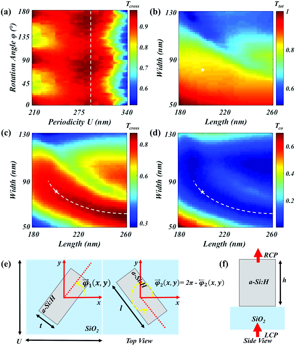
 . The phase difference (ΔΦ) between two nanoelements (Fig. 1e) at the interface can be engineered to incorporate distinct information in the forward and backward directions, which is governed by the following equations:
 are the rotation angles associated with first nanoelements in the supercell for the forward and backward directions, respectively. Similarly,
  denote the rotation angles of the second nanoelement in the supercell for the forward and backward directions, respectively as shown in Fig. 1e. Moreover,
  correspond to the desired phase maps of two distinct images. The value of σ is either +1 or −1 depending on the helicity of the incident light (with LCP or RCP respectively). In the case of incident light with LCP, the expressions of the total electric fields transmitted from a supercell (Fig. 1e) containing two nanoelements with shifted rotation angles are derived in the supplementary information and given by
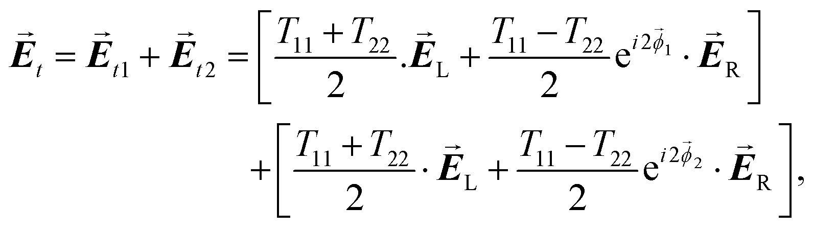


 can produce a different image in the backward direction (Fig. 3d) and no image in the forward direction (Fig. 3c). Finally, both metasurface holograms are combined to reproduce distinct holographic images on the observation plane depending on the direction of the incident light, as shown in Fig. 3e and f.
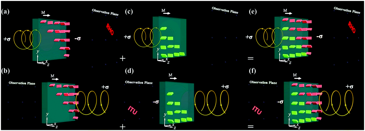
 ) diverging the scattered light in (c) the forward direction and producing the desired logo of Information Technology University “ITU” in (d) the backward direction. (e) Reproduction of the holographic image of logo “RHO” in the forward direction and (f) the holographic image of logo “ITU” in the backward direction by multiplexing two distinct metasurfaces for dual operation. At transmission sides, the diverging beam is depicted in green color and the beam containing information about the holographic images is represented in red color. Two distinct phase maps of images with logos “RHO” and “ITU” are obtained using the iterative Fourier transform method. The phase maps of these two images are compensated for the off-axis projection of holographic images. In conjunction with that, both phase maps are also modified to maintain the required phase shift for direction-multiplexing (eqn (3)). These phase maps are then combined to form the 1378 × 1378 elements matrix. This corresponds to a metasurface with a size equal to 399.62 μm2. The phase maps are combined such that the top-right half of the metasurface corresponds to the holographic image “RHO” for the forward direction and the bottom-left half is associated with the holographic image “ITU” for the backward direction.