
Nanotrapping memories
Chang-Hyun
Kim

Department of Electronic Engineering, Gachon University, 13120 Seongnam, Republic of Korea. E-mail: chang-hyun.kim@gachon.ac.kr
First published on 8th April 2019
Abstract
Electrical memories have been vital to our everyday life, and their impact will be more significant in a future that is data-centric, sensor-equipped, and artificial-intelligence-powered. This review aims at discussing advances in nanotrapping memories, a term that is coined to embrace devices that functionally rely upon embedded nanoscale charge-trapping objects. The rationalization, demonstrations, and engineering concepts suggest that nanotrapping memories position themselves as a promising platform for both traditional and bio-inspired hardware architectures, and that their strong materials emphasis fuels the upcoming interdisciplinary nanoscience research.
 Chang-Hyun Kim | Chang-Hyun Kim is an Assistant Professor of Electronic Engineering at Gachon University. He received his PhD in physics from the École Polytechnique, France, in 2013, and conducted postdoctoral research at Columbia University, the French National Centre for Scientific Research (CNRS), and Gwangju Institute of Science and Technology, before joining the faculty in 2018. His current research focuses on the development of novel electronic devices based on organic semiconductors and hybrid nanoarchitectures. Prof. Kim was a recipient of the Alliance Doctoral Mobility Award, the Prix de thèse (PhD thesis award) of the École Polytechnique, the Korean Ministry of Education Research Fellowship, and the IEEE International Symposium on Next-Generation Electronics Best Paper Award. |
1 Introduction
The Internet-of-things (IoT) is a concept that is constantly evolving, and broadly describes a network of electronic systems such as phones, TVs, home appliances, and vehicles, where each component communicates with another via the Internet to provide a highly automatized and customized service.1–4 Therefore, it represents a clear vision of an ultra-connected society and its world-wide market is expected to experience an unprecedented rapid growth.5 Not just because it sometimes aims at ‘digitizing’ the entire building or even cities,6,7 the successful deployment of the IoT is conditioned by a multitude of sectors including consumer electronics, environmental engineering, computer science, informatics, as well as policies and marketing strategies.8 In particular, materials science can contribute enormously to this developmental context, because the necessity of electronic materials and devices suitable for new applications will sharply increase.Memories are key ingredients of electronics, as they serve as a bridge between the sensing, processing, and communicating parts of any hardware architecture.9 In fact, the semiconductor memory industry is a mature one, making available a number of useful products. However, the requirements for next-generation memories should be different from those already in use, when thinking about the IoT and associated areas where the physical shape, tunability, and adaptability of devices become more critical than in traditional settings.10,11 Recognizing this opportunity, there has been a substantial expansion of research towards novel materials and multifunctional devices.12–14 Nanomaterial-based memories are an outstanding candidate for portable, wearable, infrastructure-embedded, or implantable products, because of their competitiveness for ultimate scaling-down and controllability. The state-of-the-art devices with e.g. graphene,15–17 carbon nanotubes,18–20 Si nanowires,21–23 or organic molecules24–26 are evidencing their great promise.
In this review, the phrase ‘nanotrapping memories (NTMs)’ is proposed to collectively describe a special class of nanomaterial-enabled memory technologies. Roughly speaking, NTMs refer to a range of devices incorporating nanomaterials as controllable charge traps (a more precise definition and classifications will follow). We have recently noticed remarkable progress in these particular devices as a distinct building block, which exhibits a high degree of design freedom, a favorable mechanical form factor, and excellent multifunctionality. Therefore, it is timely to deliver an overview of this emerging nanoelectronics platform, which is expected to fit well into both traditional and unconventional systems, including neuro-inspired computing.27–31
The remaining parts of the article are organized as follows. In Section 2, we first put forward a fresh look at two well-established concepts for building a solid foundation for novel memory devices. Section 3 illustrates the definition and key mechanisms of NTMs, and introduces their sub-categories. Section 4 then highlights some of the representative devices that strengthen the understanding of the operating principles and clarify the applicable areas. Section 5 offers a subjective view on how to successfully design and optimize future NTMs. Finally, Section 6 provides some concluding remarks. While NTMs can be created with various semiconductors, we restrict our attention to the organic-semiconductor-based ones, which we believe represent an ideal material combination towards mechanically flexible, low-cost/large-area-processable, and functionally tailored systems.32–36
2 Thinking differently
2.1 Traps that are helpful
Almost all traits of an organic device find their origin in the molecular nature of the active layer.38 While a van der Waals type solid is clearly attractive for low-temperature deposition and mechanical softness, characteristically weak intermolecular coupling leads to a substantially lower carrier mobility (compared to that of a bulk inorganic crystal), as well as a strong energetic disorder.39–41 As a result, a majority of the organic semiconducting mediums, which are generally prepared as a thin film, contain a large density of charge traps.42,43 Due to the same molecular landscape, these materials are also highly sensitive to interface chemistry, and specific functional groups and/or spontaneous charge transfer between the two materials can introduce additional surface traps.44–48 Taking organic field-effect transistors (OFETs) as an example, these traps are generally responsible for a large hysteresis and/or a non-negligible bias-stress effect,49 both of which are detrimental to the reliable circuit applications of transistors.Although organic-based devices have been quite notorious for trap-related problems, it is actually not the traps themselves to be blamed but their uncontrollability. For instance, Fig. 1 shows a dual-sweep transfer characteristic (gate voltage VGversus drain current ID) excerpted from a paper published in 2005 by Gu et al.37 These data were obtained from a pentacene OFET with a SiO2 dielectric. It is worth emphasizing that the observed ‘memory’ effect (i.e. two different ID levels at the same VG depending on the driving sequence) was not intended here and this particular OFET structure did not explicitly include any traditional kind of memory elements (e.g. a ferroelectric insulator or charge-storage electrode).12 Instead, the hysteresis was most likely due to the combined effects of intrinsic traps within polycrystalline pentacene and interface traps of the hydroxyl groups.50,51 Therefore, the real issue is the difficulty in having full control over these mechanisms, but if we could selectively eliminate some of the unnecessary traps while endowing the remaining traps with desired physical properties, it would eventually make up a useful memory device.
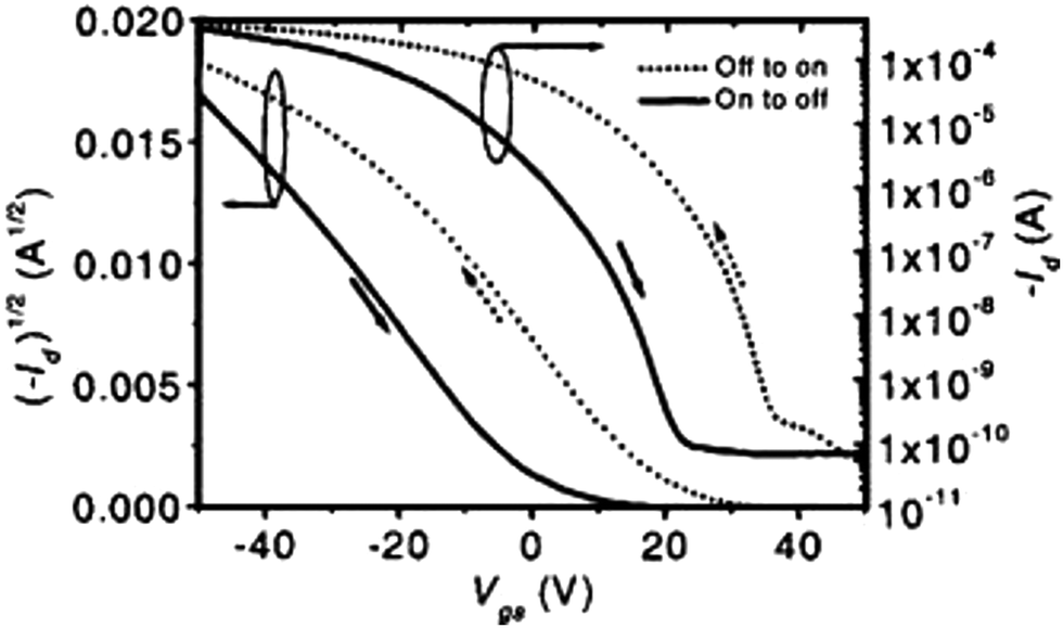 | ||
| Fig. 1 Saturation-regime transfer characteristics of a pentacene OFET showing a considerable hysteresis (measured at a fixed drain voltage of −50 V). Id: drain current, Vgs: gate voltage. Reproduced with permission. Copyright 2005, American Institute of Physics.37 | ||
In fact, smart and purposeful engineering of trapping sites has become a reality thanks to the advances in materials and interface engineering,52 and emerging NTMs fully utilize this possibility of introducing and adjusting charge traps of different natures for the realization of advanced memory structures.
2.2 ‘Distributed’ floating gates
Since Kahng and Sze proposed the first nonvolatile memory device in 1967,54 the concept of ‘floating gate’ has been broadly exploited.55 As a classical picture of EEPROM (electrically erasable and programmable read-only memory) in Fig. 2 suggests, a floating gate refers to the (usually metallic) electrode that is sandwiched between two dielectrics.53 The name originates from the fact that a floating gate is usually embedded in a single dielectric medium (the electrode looks like it is ‘floating’ inside, which actually blurs the distinction between the two oxides). What is expected from this characteristic stack dictates the operating mechanism. Whether it is on a bulk MOSFET or a thin-film FET, the application of a VG (at the control gate) leads to an electrical charging or discharging of the floating gate either by attracting charges from the channel or by releasing charges into the channel. This exchange of carriers is mediated by quantum mechanical tunneling or other injection mechanisms.56 Eventually, these charges at the floating gate affect the applied gate field, thus altering the threshold voltage (VT) of the transistor. In short, the data in a cell is stored as a charged state of the floating gate, which is read as a terminal voltage or a corresponding current.57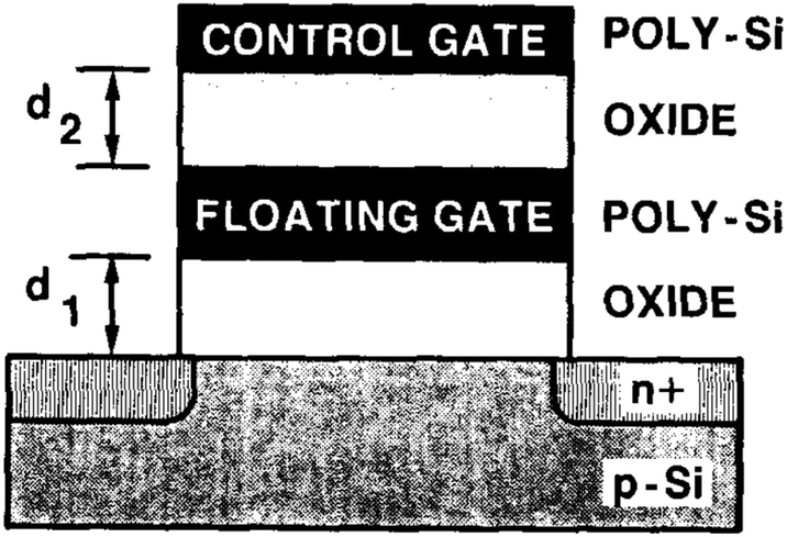 | ||
| Fig. 2 Cross-sectional illustration of a traditional floating gate EEPROM device. The thicknesses of the tunneling and blocking oxides are denoted as d1 and d2, respectively. Reproduced with permission. Copyright 1989, Institute of Electrical and Electronics Engineers.53 | ||
The reason for revisiting the traditional floating gate effect here is that the basic mechanism is largely shared by NTMs. However, there are major differences that arise in terms of shapes and locations of floating materials, as well as their fabrication techniques, which are decisive factors that render NTMs highly tunable. First, nanomaterials in an NTM do not necessarily form a physically continuous layer while they can safely function as distributed and disconnected floating nodes. This underlines the possibilities for facile processing of a hybrid region where both dielectric and trapping materials are tightly intermixed. Second, the locations of floating gates can vary significantly from one device to another. A key to the function is the role of nanomaterials as externally controllable charge reservoirs, so they can even be placed in the semiconductor if efficient charge transfer can be maintained at the nanoscale. This aspect may weaken the appellation of floating ‘gates’ since the trapping materials do not always have to neighbor the gate or we can even build a device without any gate. In any case, when these materials are fully surrounded by a host matrix (either dielectric or semiconductor) and utilized as indirectly driven capacitors, the word choice is justified by both their appearance and mechanistic similarities. Third, in a classical floating gate device (such as that in Fig. 2), the three core layers (two dielectrics and the floating gate) are formally deposited, but in NTMs, manufacturing can be simplified in the cases where a nominally single material provides several properties. We will see below systems that employ surface self-oxidation or preliminary conformal capping for these purposes.
3 Definition and key mechanisms
The definition of an NTM is visually accentuated in Fig. 3. It broadly designates thin-film electronic memory devices, either diode- or transistor-type, where a variety of reduced-dimensional architectural ingredients function as structurally and operationally controllable charge-trapping physical sites. It differs from conventional memories in terms of material integrations, device structures, and extractable functionalities while it does not necessarily add a separate family to the traditional tree of memory technologies.58 Rather, it is regarded as a new nanotechnological approach to offering improved or hybridized performances in several existing platforms.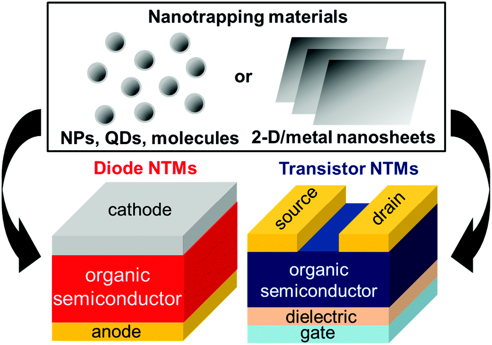 | ||
| Fig. 3 Concept of the NTM technology. The charge nanotrapping mechanism is assumed by various 1-D or 2-D materials with different natures and compositions. These nanoarchitectures are incorporated in the active layer or at the interfaces of a diode or transistor device to manifest memory functionalities. | ||
From an electrical point of view, what is common in all different types of NTMs, many of which will be discussed in the next section, is that the incorporated nanomaterials play a crucial role in determining the macroscopic properties despite their small volume fraction. This important characteristic stems from their efficient charge-trapping and detrapping capabilities at normally non-trapping pathways. Fig. 4 illustrates two charge-trapping mechanisms relevant to NTMs. The energy-offset mechanism refers to the energetically driven movement of charge carriers to a stable trapping state and their subsequent immobilization. The trapped carriers have the chance to be detrapped back into the transport level getting thermal energy. This mechanism is dominant in a composite-type channel where a semiconductor and nanotraps form a uniformly mixed phase and the trap material provides a sufficiently deep quantum-well-like structure. The field-induced tunneling mechanism becomes critical when the nanotraps are surrounded by a dielectric (either as a surface capping or an external film). Depending on the direction and strength of the applied field, carriers tunnel into the nanotraps or escape back into the channel. While in Fig. 4 we employed the case of a biased diode and an accumulated transistor for the respective mechanism, it is for illustration purposes only, and the actual material characteristics and device geometry dictate which mechanism outperforms the other one, and both mechanisms can occur in both devices. When the trapping materials are uncharged or empty, the memory is said to be in its ‘erased state’ and it provides a certain level of intrinsic terminal current. After charging them in different fashions, the device is now in the ‘programmed state’ and the current becomes altered. This is a generic explanation that applies to both diode and transistor NTMs. For transistors, a VT shift is often evoked to mention a state change. Although it seems natural to observe a lower current level in the programmed state (because we are talking about charges trapped), this is not always true because there are cases when the conduction carriers and trapped carriers are not of the same type, thus providing a larger density of counter charges and current when traps are occupied. Therefore, it is highly recommended to carefully establish a proper operating mechanism and analysis framework for each NTM, especially when we are presenting totally new materials or geometries.
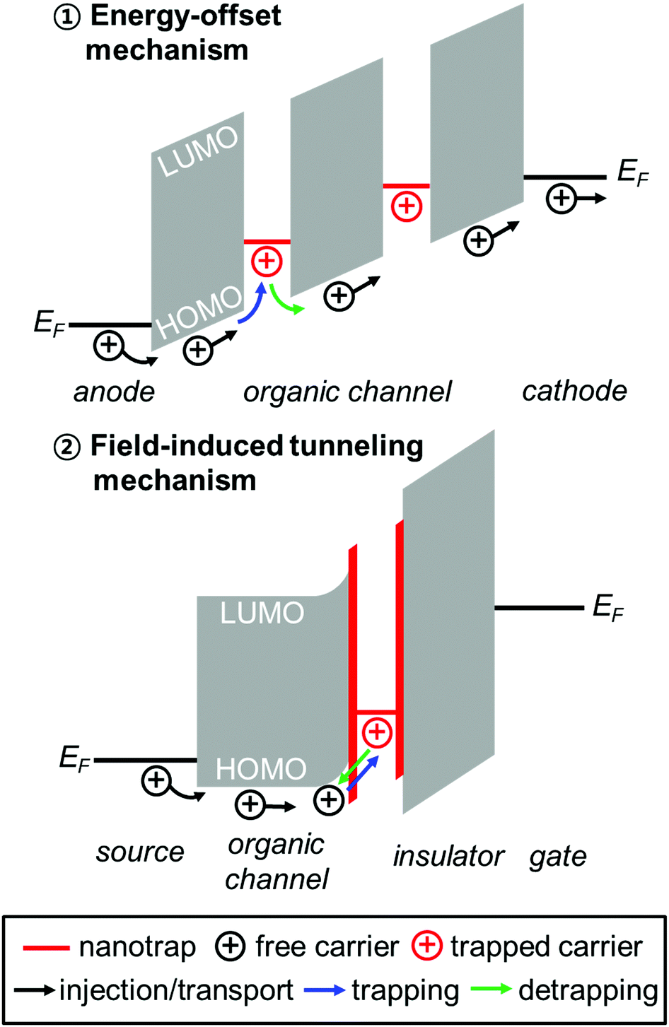 | ||
| Fig. 4 Energy diagrams illustrating characteristic charge-trapping and detrapping mechanisms. A hole-transporting semiconductor is assumed. Because of the dielectric nature of an organic medium, straight HOMO and LUMO levels appear in the diode architecture and the source injection barrier has direct implications in a transistor (EF: Fermi level of the metal electrode). | ||
Given the many different combinations of trapping materials, semiconductors, and device layouts, there are a virtually unlimited number of NTM variants. Nonetheless, in view of recent reports, we suggest categorizing them into two groups: NTMs with metallic nanostructures and those with carbon-based nanostructures. We will, from now on, exclusively deal with the devices that fall into either of these two sub-categories. Note that, among all possible structures (see Fig. 3), NTMs with non-carbon semiconducting trapping media will not be reviewed as they have not yet been investigated much. However, recently developed inorganic quantum dots (QDs) or hybrid perovskites are worth considering for a future generation of NTMs.59–62
4 Recent developments
Here, a systematic overview of NTMs is provided with reported examples. Our focus is to clarify the materials choice, fabrication techniques, structural designs, interface phenomena, and physical mechanisms of representative systems. The uniqueness of each device will be also evaluated with its technological implications reassessed. In particular, we will separately discuss the applications of NTMs as conventional nonvolatile memory elements (used in traditional computing architecture) and as bio-inspired synaptic devices that are the foremost elements for the realization of neuromorphic computing. Note that, while we will be introducing many historically important devices, those that are showcased in Fig. 5–8 are the most recent achievements (published within the last five years) that best represent the current status of the field.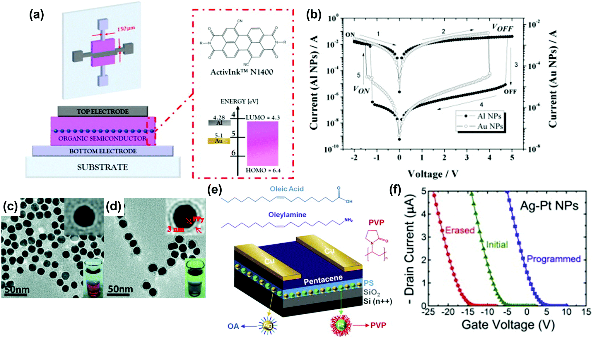 | ||
| Fig. 5 Metal-nanostructure NTMs: conventional applications. (a) Device structure of an n-type diode memory with Al or Au NPs. The molecular structure of the semiconductor and the relevant energy levels are given. (b) Cyclic current–voltage characteristics showing a resistive switching behavior. (a and b) Reproduced with permission. Copyright 2015, Elsevier.63 TEM images of (c) Au NPs and (d) Au@PPy core–shell NPs. (c and d) Reproduced with permission. Copyright 2018, Wiley-VCH.64 (e) Structure of a pentacene OFET memory with bimetallic NPs. (f) Shift of the transfer curve upon gate programming and erasing (measured at a drain voltage of −3 V). (e and f) Reproduced with permission. Copyright 2015, Elsevier.65 | ||
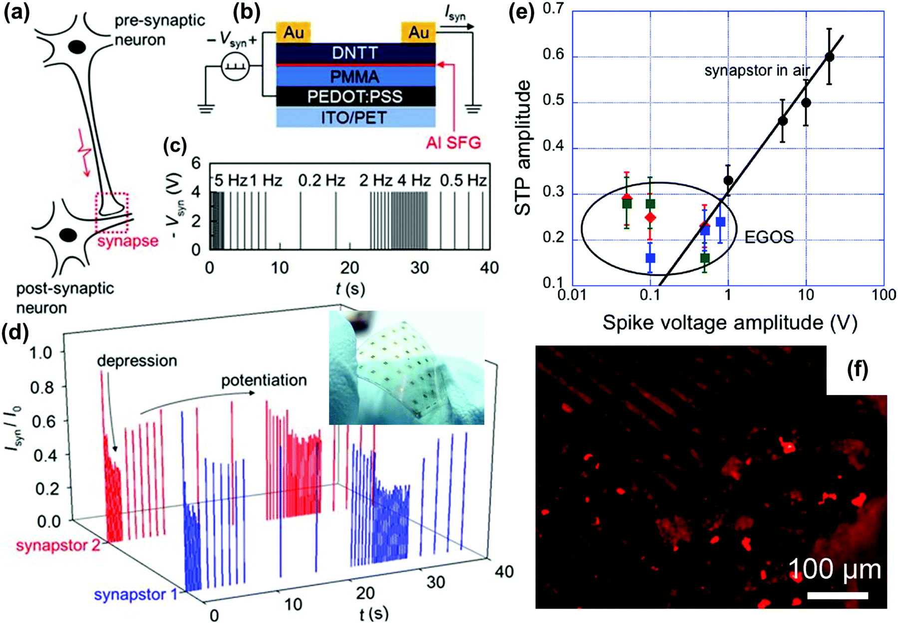 | ||
| Fig. 6 Metal-nanostructure NTMs: neuromorphic applications. (a) A simple illustration of the biological signal transmission between neurons via a synaptic junction. (b) Structure and electrical configuration of the DNTT synaptic transistor (synapstor). (c) Spike-type input voltage signals. (d) Time-varying output currents measured from two different synapstors showing the STP behavior (inset: photograph of a flexible device array). (a–d) Reproduced with permission. Copyright 2016, Nature Publishing Group.69 (e) The STP response amplitude versus the absolute value of the spike amplitude in pentacene–Au NP transistors. (f) Immuno-fluorescence image of SH-SY5Y grown and differentiated on EGOS. The red color is yielded by Alexa Fluor 594 immuno-label staining β-III tubulin. (e and f) Reproduced with permission. Copyright 2016, Elsevier.70 | ||
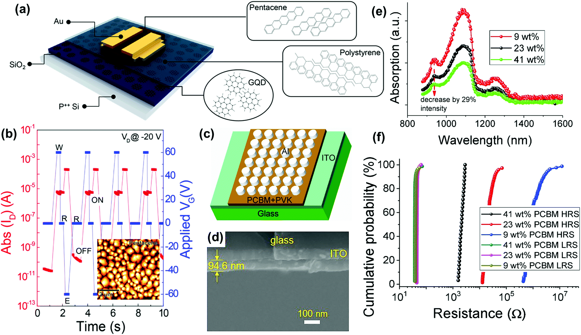 | ||
| Fig. 7 Carbon-nanostructure NTMs: conventional applications. (a) A structural illustration of the GQD-based memory transistor along with the chemical structures of the materials. (b) Repeated WRER cycling test using sequential VG signals of 60, 0, −60, and 0 V at a VD of −20 V. Inset: AFM topography of the pentacene layer. (a and b) Reproduced with permission. Copyright 2016, Institute of Physics.80 (c) Structure of the resistive memory based on a PCBM + PVK active layer. (d) Cross-section of the device with 9 wt% PCBM. (e) Optical absorption spectra of the composite films with different PCBM contents. (f) Statistical analysis of the resistances at HRS and LRS. (c–f) Reproduced with permission. Copyright 2019, Elsevier.81 | ||
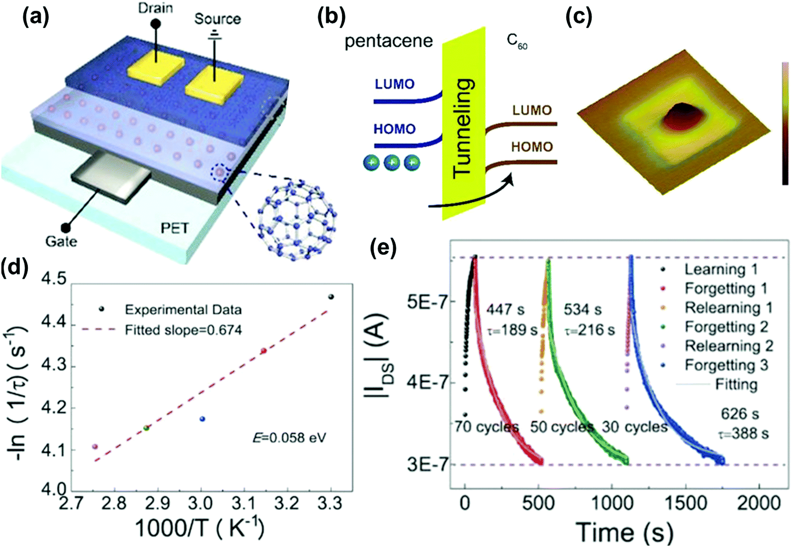 | ||
| Fig. 8 Carbon-nanostructure NTMs: neuromorphic applications. (a) The structure of the flexible synaptic transistor with C60 floating gates. (b) Gate-induced hole-trapping mechanism. (c) KPFM mapping of the trapping processes. (d) Temperature dependence of the relaxation time (E: activation energy). (e) Physiological learning, forgetting, and relearning experiences of the device. (a–e) Reproduced with permission. Copyright 2018, Wiley-VCH.90 | ||
4.1 NTMs with metallic nanostructures
When a metal is embedded into a semiconductor, it provides a material-specific Fermi level that interacts with the transport levels of the surrounding host. Many organic semiconductors have a sizeable band gap, so a general energy diagram would facilitate carrier trapping by this metal rather than an injection from it (more discussion in Section 5.1). An early report by Ma et al. published in 2002 revealed a diode memory characteristic from an organic/metal/organic tri-layer sandwiched between an anode and a cathode.66 A relatively thick Al layer (20 nm) was coupled with the organic semiconductor 2-amino-4,5-imidazoledicarbonitrile (AIDCN). Surprisingly, this unusual device exhibited a clearly identifiable ‘forming’ process and programmable current levels, which are seen in today's memristors.14 The exact mechanism was not fully accounted for at this time, but it is likely that both the intrinsic trapping at Al/AIDCN and the floating gate effect through the oxidized Al contributed to the memory behavior. This result stimulated further research and an important trend was to reduce the dimension of the metallic center by incorporating, for instance, metal nanoparticles (NPs). Many later studies investigated this organic–metal hybrid diode memory,67 and among them, that by Bozano et al. published in 2005 demonstrated a series of tunable memory devices by varying both the semiconducting material and the spatial distributions of the NPs inside the active layer.68In 2015, Casula et al. reported on an air-stable, electron-transporting diode NTM (Fig. 5a and b).63 The authors fabricated a vertical ITO (indium tin oxide)/N1400/NPs/N1400/Ag stack on glass with N1400 being the commercial name for a core-cyanated perylene derivative. The middle layer was composed of vacuum-evaporated Al or spray-coated Au NPs, to provide tunable morphologies and energy levels (Fig. 5a). Despite a substantial difference in their work functions, Al and Au NP based diodes showed similar resistive switching behaviors, as shown in Fig. 5b. We infer that this may reflect actual dissimilarities in the shapes and distributions of the NPs, and a thin surface alumina could also play a role. A high resistance ratio over 103 was obtained between on- and off-states, and a long data retention time on the order of 107 s was confirmed (for Au-NP devices). Importantly, the devices proved to be extremely stable in air, maintaining a reliable performance up to 16 months and enduring over 500 on–off cycling tests. Therefore, this device represents a promising platform that can satisfy a range of performance criteria (including long-term stability) critical to real applications.
A specific surface state (e.g. impurities or native oxides) may substantially contribute to the charge transfer kinetics at the metal/semiconductor interface, so probing and exploiting such nanoscale interfaces has become an important challenge. In this context, recent research on intentional pre-capping of NPs is worth discussing. In 2018, Zheng et al. demonstrated programmable negative differential resistance (NDR) in coplanar diodes made of self-assembled Au@polypyrrole (PPy) core–shell NPs (Fig. 5c and d).64 They achieved a bottom-up synthesis of hybrid NPs from cationic radicals on a prepolymerized PPy chain adhering to electronegative Au. By this method, NP aggregation was avoided, and a uniform dispersion with a well-defined capping structure was obtained, as shown in the transmission-electron microscopy (TEM) image in Fig. 5c and d. A simple solution deposition completed the device, and they could selectively alter the core NP size (13 to 18 nm) and the polymer thickness (2 to 5 nm) to modulate the NDR characteristics.
The NPs-in-organic concept has also been widely employed in transistor devices.71,72 Similar to diodes, the chemical nature, shape, and distribution of the NPs are shown to all be critical to the electrical properties, while a fundamental difference to take into consideration is the surface-conduction mechanism in FETs with a substantially larger carrier mobility (compared to bulk transport in diodes).73 Also, the structural uniqueness of an OFET allows for the integration of NPs within the gate insulator, drawing additional possibilities for device engineering.74–77 In 2015, Zhang et al. reported on advanced OFET NTMs incorporating bimetallic NPs (Fig. 5e and f).65 These authors compared three cases: Ag-only, Pt-only, and Ag–Pt bimetallic NP arrays in the polystyrene (PS) dielectric. As shown in Fig. 5e, the Ag and Pt NPs were stabilized by oleic acid/oleylamine (OA) and polyvinylpyrrolidone (PVP), respectively. Pentacene was used as a p-type molecular semiconductor, in conjunction with Cu source/drain electrodes. A major finding was that the bimetallic NPs produce a synergistic effect. All three systems exhibited both positive and negative VT shifts upon programming and erasing gate pulses. Interestingly, the memory windows (i.e. the entire VT shift range upon programming–erasing) of the Ag- and Pt- samples were 8.8 and 9.9 V, respectively, while it increases up to 18.7 V when both particles are present (Fig. 5f). This enhancement was rationalized by more hole-selective trapping of Ag and electron-selective trapping of Pt, cooperating to hold the largest density of trapped charges in the bimetallic case. This result suggests that the hybridized use of nanotrapping materials can be a great strategy for the improvement of NTMs. Another possible location of a trapping layer in an OFET is at the interface between the gate dielectric and the semiconductor.78 In 2016, our group published protein-capped Au NPs directly immobilized between SiO2 and pentacene, which made up highly adjustable and large-area uniform memory transistors thanks to the dual properties of the protein molecules as a film-forming agent and an efficient tunneling dielectric.79
Neuromorphic engineering is an emerging research area, which aims at building electronic systems that mimic the mechanisms of biological neurons and their interactions (Fig. 6a).27–31 It is expected that the ultra-parallel and extremely energy-efficient function of neurons can revolutionize traditional computing architecture. Synaptic devices are key elements in an artificial neural network, and different memory structures with synapse-mimicking functionalities have been demonstrated. In 2016, our group reported on an NTM-type synaptic transistor (synapstor) on plastic (Fig. 6a–d).69 Here, a few-nm-thick Al nanosheet was inserted between a poly(methyl methacrylate) (PMMA) dielectric and a dinaphtho[2,3-b:2′,3′-f]thieno[3,2-b]thiophene (DNTT) semiconductor.82–84 The thermally evaporated conformal Al layer was readily surface-oxidized to become an Al SFG (self-formed floating gate), for the molecular channel to stay stable without electrical shorting (Fig. 6b). More importantly, the ultra-thin Al2O3 allowed for highly dynamic gate-driven trapping and natural detrapping of holes in the intact core Al region. Thanks to this structural arrangement, we successfully demonstrated the short-term plasticity (STP) of biological neurons in our devices, as shown by the constantly decreasing (depression) or increasing (potentiation) currents upon modulating the frequency of the input spike trains (Fig. 6c and d). This study therefore raised the potential of mechanically flexible electronics for wearable neuromorphic systems.
Building upon a series of their earlier work,85–87 Desbief et al. reported in 2016 on an electrolyte-gated organic synapstor (EGOS) interfaced with real neurons (Fig. 6e and f).70 In this study, an NTM structure is found in the pentacene–Au NP mixed active region. These authors specifically compared two driving schemes: the bottom-gate solid-state driving (‘synapstor in air’ in Fig. 6e) and the top electrolyte-gating using 0.1 M NaCl solution in water (‘EGOS’ in Fig. 6e). While the STP was systematically observed in both cases, the magnitude of the operating voltage varied significantly. The synapstors in air required a large voltage around 10 V, but the EGOS operated with a minimal voltage as low as 50 mV due to the strong capacitive coupling through electric double layers (EDLs) (Fig. 6e).88 It is important to note that this voltage range is close to what the biological neurons transmit in their action potentials. Therefore, they made an attempt to build a direct neuronal interface using the EGOS. The suitability of a pentacene–Au film was tested by growing human neuroblastoma stem cells SH-SY5Y and NE-4C on top, and it was found to be a biocompatible substrate towards these cells (Fig. 6f). The device STP characteristics were not significantly affected by cell growth and differentiation, implying that neurons are weakly coupled to the transistor. We believe that the replacement of a biological synapse by an electronic one, or neuroprosthetics, might not be within the widespread interest of neuromorphics, but it might be something that organic systems will be able to ultimately accomplish.
4.2 NTMs with carbon nanostructures
The devices in which carbon-based nanomaterials undertake the nanotrapping function are discussed here. They are similar to the metal-based ones described above in that the shapes, properties, and locations of nanotraps are tailored to meet the specific performance requirements. Nonetheless, they can, in principle, provide a wider electronic tunability, because we can choose from 2-D materials such as graphene, semiconducting components (e.g. fullerenes) with a useful band gap, as well as mixed-dimensional, hybridized nanostructures.89In 2015, Park et al. reported on the controlled growth of a graphene charge-floating gate for memory transistors.91 They systematically varied the chemical vapor deposition (CVD) time of graphene on Cu foil from 1 to 60 s, to obtain partially connected ‘discrete’ nanosheets. An optimum material was obtained under the 40 s conditions to guarantee both a good coverage and in-plane discontinuity, which was claimed to be important for long-term charge storage. This graphene was transferred to be inserted between two dielectrics (SiO2 and PS), on which a pentacene channel and Au source/drain electrodes were evaporated to complete the device. The insertion of graphene resulted in a hysteresis in the transfer curves, which was absent in the control device. Therefore, an NTM-type operation was successfully demonstrated, with graphene serving as distributed charge traps. The transistor exhibited a large memory window (∼40 V) and a long data retention time over 105 s. In 2016, Ji et al. proposed an OFET memory with a solution-processed graphene quantum dot (GQD) layer (Fig. 7a and b).80 Physical and chemical nanoengineering of graphene is an efficient technique to tune its electrical properties,92 and these authors utilized a modified thermal plasma jet method to produce high-crystallinity GQDs with suppressed oxidation. The materials were spin-cast onto SiO2 and covered with a thin tunneling PS dielectric (Fig. 7a). The PS also planarized the QD surfaces, important for the growth of a pentacene film (inset of Fig. 7b). The final devices operated robustly with the on–off current ratio in excess of 105, the retention time over 104 s, and the confirmed endurance to 100 write/erase cycles. Fig. 7b is the result of a repeated write–read–erase–read (WRER) cycling test, showing the systematic transition between the on and off states. The electrical behaviors were explained by quantum confinement and level splitting in the GQDs, offering a carrier-trapping capability up to 7.2 × 10¹² charges per cm2. These and related research evidence that graphene, prepared by various synthetic routes and with different shapes, can be a high-performance trap medium for both diode and transistor NTMs,93,94 expanding its applicability beyond transparent electrodes.
Fullerene (C60) and its derivatives have also received growing attention as a molecular memory ingredient.95–98 A recent diode application can be found in the article by Sun et al. published in 2019 (Fig. 7c–f).81 Here, a vertical ITO/PCBM + PVK/Al stack was constructed on glass, where PCBM + PVK means a composite layer between [6,6]-phenyl-C61-butyric acid methyl ester (PCBM) and poly(N-vinylcarbazole) (PVK) (Fig. 7c). Both of the organic semiconductors were dissolved in dichlorobenzene and blended in the solution phase, with three different mixing ratios (9, 23, and 41 wt% PCBM). They were co-deposited by spin-coating to form a homogeneous active layer of less than 100 nm, as shown by the scanning electron microscopy (SEM) image in Fig. 7d. The authors specifically addressed the effect of the blending ratio on the electrical properties. In optical absorption measurements on the active films (Fig. 7e), the weak absorption band around 923 nm decreased at high PCBM contents, manifesting an overall favorable charge transfer between the donor PVK and the acceptor PCBM at low concentrations. All the diode devices behaved as a resistive switching memory, with a strong ratio effect. As shown in Fig. 7f, the resistance ratio between the high-resistance state (HRS) and the low-resistance state (LRS) was the highest for the 9 wt% sample, with a value exceeding 104, confirming that electronic coupling is the most pronounced under this condition. The devices were also shown to be highly non-volatile with an estimated retention time over 105 s. This study therefore reveals that a purely organic blend with a substantial internal energetic mismatch can produce an all-organic NTM, by affording efficient charge trapping and retention even without any dielectric capping or blocking interlayer.
Neuromorphic applications of carbon-based NTMs have been suggested very recently. In 2018, Ren et al. reported on gate-tunable synaptic plasticity in fullerene composites (Fig. 8).90 They synthesized a hybrid C60/PMMA nanotrapping film by solution processing. As shown in Fig. 8a, such a film was inserted between an Al2O3 blocking insulator and a pentacene channel, and Ag gate and Au source/drain electrodes were used for the transistor. All materials were low-temperature-processed to build a plastic device, and the combination of thin dielectrics (30 nm Al2O3 and 75 nm PMMA) allowed for low-voltage operation at around 5 V. Following the conventional floating gate mechanism (reviewed in Section 2), the uniformly distributed fullerenes served as gate-controllable charge-trap centers. Under a negative VG, holes from pentacene could tunnel into C60 (Fig. 8b), and under a positive VG, electron trapping occurred. Fig. 8c shows the Kelvin probe force microscopy (KPFM) image visualizing both a hole-trapping region (center) and an electron-trapping region (surroundings) in the C60/PMMA film, with a measured potential difference of ∼500 mV between the two regions. After charging the fullerene nanotraps with either type of carriers, the natural detrapping (or relaxation) process was monitored. Fig. 8d is an Arrhenius analysis showing that electron detrapping is thermally activated, equivalent to the relaxation time (τ) decreasing with a temperature (T) increase. The manipulation of the carrier trapping at the time domain was combined with the natural relaxation to mimic a number of biological synaptic functions, e.g. excitatory postsynaptic current (EPSC), paired-pulse facilitation/paired-pulse depression (PPF/PPD), and transition from short-term to long-term potentiation. An interesting demonstration is shown in Fig. 8e, for the three repeated cycles of learning and forgetting. Here, a learning period corresponds to current enhancement by multiple positive VG pulses, and forgetting is a detrapping relaxation. It was found that, between the two fixed current levels, a smaller number of ‘learning’ pulses were required with a slower relaxation when the process is repeated, reminding us of relearning with a human brain to keep old knowledge alive.
5 Design considerations
The comprehensive picture established in the previous section now allows us to see NTMs as a rapidly growing subject. Therefore, it seems difficult to grasp its full potential at this stage, and tremendous new opportunities are foreseeable. In this section, several key insights into how to create new devices with tailored functionalities are provided, as a guideline for future research endeavors.5.1 Energetic alignments
As detailed in our previous reviews,33,47 organic semiconductors are intrinsically reliant on an external charge supply due to their dielectric nature. Therefore, the energetic position of the frontier orbitals is the first to consider especially when designing an NTM with trapping inside the active layer (such as those in Fig. 5a and 7c, or NPs-in-channel OFETs71,72). When we incorporate a metallic nanotrap, its proper functioning as traps is guaranteed when its Fermi level is positioned within the band gap of the contacting semiconductor.56 In this sense, energetically deeper traps can provide a more pronounced effect with stronger device non-volatility (slower detrapping). In other words, the choice of a good ‘trapping’ metal for a given semiconductor generally goes in the opposite direction from how to select an efficient ‘injecting’ electrode. One can therefore refer to the available database (which actually mostly served the latter purpose) on the HOMO and LUMO levels of semiconductors and Fermi levels of metals in advance to pick ideal combinations.47,99,100 For NTMs with a carbon-containing semiconducting trap, at least one of its frontier orbitals should be placed within the band gap of the host matrix to ensure efficient trapping.When a dielectric is present between the nanotrap and the active material, either intentionally (e.g. self-assembled monolayers, core/shell architecture) or uncontrollably (e.g. native oxidation, mostly when Al is used), the pure energetic balance between the two media may eventually become less critical, because the tunneling and floating gate effects will enable the core to accommodate and hold trapped carriers.79
Relevant energy levels can be substantially affected by processing or by an electric field, implying another important aspect to take into account. For example, Mosciatti et al. reported in 2015 on a multifunctional polymer–graphene transistor exploiting one of these secondary effects.101 In this study, liquid-phase exfoliated graphene (LPE-G) was directly solution-deposited on a dielectric to form disconnected islands, onto which a polymer semiconductor made up a transistor channel. It was found that the ionization energy of LPE-G is highly sensitive to post-deposition thermal annealing, with a value changing from 4.8 to 5.7 eV. Therefore, it was possible to use LPE-G either as a nanotrapping material or a conductive bridge inside the semiconductor, depending on its energy. Graphene's work function is also known to be strongly field-dependent, and this property gave birth to novel vertical heterojunction triodes.73 Therefore, it is theoretically reasonable to expect a dynamic change of trapping levels in graphene or related materials inside an NTM under operating conditions.
5.2 Hierarchical features
Due to the soft molecular nature, the growth of an organic film is strongly affected by the underlying substrate.102 Furthermore, the nanoscale growth interface is believed to have a sequential bottom-up effect on the meso- to macroscopic properties through hierarchical mechanisms that are pronounced in organic-based systems. For instance, the molecular orientation of the same material, which can be tuned by the substrate chemistry, can have a broad impact on the injection barrier, carrier mobility, dielectric constant, emissive properties, and so on.44,45,103So, when incorporating a nanotrapping material, a careful consideration of its possible effects at various length scales is recommended, as it will enlighten an optimum material choice and an ideal device structure. Previous reports show that, when NPs are placed on a dielectric in a bottom-gate transistor, their roughness can prevent the growth of a high-mobility channel, and a trade-off between the memory and transport parameters may appear.79,85 Therefore, sophisticated interface engineering is key. For instance, introducing specific chemical anchoring groups to a metal or dielectric surface has been an efficient approach to guiding crystallization and improving ‘planar’ organic devices.46 We believe that a similar technique can be used in the context of NTMs, for the surface-functionalized nanotraps to provide an additional role as growth initiators and morphological modifiers, even though a more complex 3-D spread of the hierarchical forces will need to be elaborated.
5.3 Application horizons
To meet the increasingly strict requirements of mobile and wearable products, we can envision a newer generation of NTMs with additional potentially useful functionalities.Firstly, known optical properties of nanomaterials can be utilized to make an optically controllable NTM. Optical memories are gaining increasing attention, because they have promise for fast and low-power programming and readout. For instance, a flexible optical memory transistor with over 256 distinct levels was demonstrated in 2016 by Leydecker et al. using a photochromic organic blend.104 Nanoplasmonic effects of metal NPs and enhanced light–matter interactions are well-documented in solar cell research.105 Therefore, plasmonic improvement of optical sensitivity in an organic–NP hybrid channel can be useful to construct high-performance photonic NTM structures.
Secondly, traditionally separated sensing and memory parts can be ideally merged into a single device. In particular, the development of bio-NTMs can be an interesting idea. In 2017, our group proved the biocompatibility of protein-self-assembled Au NPs,106 the same material that was initially employed as a nanotrapping electrical component.79 Many other reports support the possibility of combining memory and biological phenomena, such as those on deoxyribonucleic acid (DNA)–Ag nanocomplex memristors,107 hysteresis-based Si nanowire biosensors,108 and biodegradable skin-inspired resistive switching memories.109
Thirdly, the energy consumption has not been addressed much, so the minimization of program/read voltages and static dissipation should be given a higher priority for technological advancements. Our expectation is that the characteristic operation relying on small-sized elements in NTMs would allow for the extreme scaling-down of the active layer and/or dielectric for a very-low-voltage device, and the inherently energy-efficient neuromorphic scheme could well serve this purpose. The ultimate goal in this direction might be a fully self-powered operation, enabled by flexible and ultra-light-weight energy harvesters (e.g. photovoltaics, thermoelectrics, etc.) integrated on-site along with sensing and memory components.110
We note that future research should aim at the areas that ideally leverage the unique properties of NTMs beyond traditional memory platforms. In this regard, a stronger emphasis on neuromorphic devices is deemed natural, given both the high promise of the technology and potentially many unrealized ways to combine nanotrapping and neuronal regimes. For the next-generation NTM synapses, structural miniaturization for biological signal compatibility, interface hybridization for operational stability, and cellular sensing and stimulating capabilities for prosthetic use can be some of the key drivers.
6 Conclusion
This review is intended to conceptualize NTMs and increase their visibility in nanoscience and electronics research. Although various devices discussed here might be originally developed under different names and motivations, a close look at their operating principles makes it logical and useful to group them into one technological stream and project their future in a unified framework. The importance of data and intelligent systems will continue to increase in our society, and it is believed that NTMs, with their versatility and flexible performances, can become a particularly promising candidate for next-generation memory technologies and unconventional on-demand platforms. Furthermore, it is anticipated that NTMs will grow to represent a cutting-edge interdisciplinary field with a clear target application, which therefore has the capacity to steer strong research efforts towards the discovery of ideal nanoscale materials and their advanced properties.Conflicts of interest
There are no conflicts to declare.Acknowledgements
This work was supported by the National Research Foundation of Korea (NRF) grant funded by the Korean government (Ministry of Science and ICT) (NRF-2019R1C1C1003356).References
- A. Zanella, N. Bui, A. Castellani, L. Vangelista and M. Zorzi, IEEE Internet Things J., 2014, 1, 22 Search PubMed.
- I. C. L. Ng and S. Y. L. Wakenshaw, Int. J. Res. Mark., 2017, 34, 3 CrossRef.
- D. Minoli, K. Sohraby and B. Occhiogrosso, IEEE Internet Things J., 2017, 4, 269 Search PubMed.
- A. Čolaković and M. Hadžialić, Comput. Netw., 2018, 144, 17 CrossRef.
- M. Gidlund, S. Han, E. Sisinni, A. Saifullah and U. Jennehag, IEEE Trans. Ind. Inform., 2018, 14, 2194 Search PubMed.
- P. Spachos, I. Papapanagiotou and K. N. Plataniotis, IEEE Signal Process. Mag., 2018, 35, 140 Search PubMed.
- F. Montori, L. Bedogni and L. Bononi, IEEE Internet Things J., 2018, 5, 592 Search PubMed.
- C. Metallo, R. Agrifoglio, F. Schiavone and J. Mueller, Technol. Forecast. Soc. Chang., 2018, 136, 298 CrossRef.
- A. K. Sharma, Semiconductor Memories: Technology, Testing, and Reliability, IEEE Press, New York, NY, 2002 Search PubMed.
- B. Prince and D. Prince, Memories for the Intelligent Internet of Things, Wiley, Hoboken, NJ, 2018 Search PubMed.
- H. Oh, J.-H. Yang, G. H. Kim, H. Lee, B.-H. Kwon, C. Byun, C.-S. Hwang, K. I. Cho and J.-I. Lee, J. Inf. Disp., 2018, 19, 165 CrossRef CAS.
- P. Heremans, G. H. Gelinck, R. Müller, K.-J. Baeg, D.-Y. Kim and Y.-Y. Noh, Chem. Mater., 2011, 23, 341 CrossRef CAS.
- R. C. G. Naber, K. Asadi, P. W. M. Blom, D. M. de Leeuw and B. de Boer, Adv. Mater., 2010, 22, 933 CrossRef CAS PubMed.
- H. S. P. Wong, H.-Y. Lee, S. Yu, Y.-S. Chen, Y. Wu, P.-S. Chen, B. Lee, F. T. Chen and M.-J. Tsai, Proc. IEEE, 2012, 100, 1951 CAS.
- X. Wang, W. Xie and J.-B. Xu, Adv. Mater., 2014, 26, 5496 CrossRef CAS PubMed.
- F. Hui, E. Grustan-Gutierrez, S. Long, Q. Liu, A. K. Ott, A. C. Ferrari and M. Lanza, Adv. Electron. Mater., 2017, 3, 1600195 CrossRef.
- S. Lee, Y. Lee, S. M. Kim and E. B. Song, Carbon, 2018, 127, 70 CrossRef CAS.
- D. Son, J. H. Koo, J.-K. Song, J. Kim, M. Lee, H. J. Shim, M. Park, M. Lee, J. H. Kim and D.-H. Kim, ACS Nano, 2015, 9, 5585 CrossRef CAS PubMed.
- D. C. Gilmer, T. Rueckes and L. Cleveland, Nanotechnology, 2018, 29, 134003 CrossRef CAS PubMed.
- L. Li and D. Wen, Nanomaterials, 2018, 8, 114 CrossRef PubMed.
- B.-H. Lee, D.-C. Ahn, M.-H. Kang, S.-B. Jeon and Y.-K. Choi, Nano Lett., 2016, 16, 5909 CrossRef CAS PubMed.
- K. Saranti, S. Alotaibi and S. Paul, Sci. Rep., 2016, 6, 27506 CrossRef CAS PubMed.
- D. Lim, M. Kim, Y. Kim, J. Cho and S. Kim, IEEE Trans. Electron Devices, 2018, 65, 1578 CAS.
- W. Li, M. Yi, H. Ling, F. Guo, T. Wang, T. Yang, L. Xie and W. Huang, J. Phys. D: Appl. Phys., 2016, 49, 125104 CrossRef.
- L. Song, Y. Wang, Q. Gao, Y. Guo, Q. Wang, J. Qian, S. Jiang, B. Wu, X. Wang, Y. Shi, Y. Zheng and Y. Li, ACS Appl. Mater. Interfaces, 2017, 9, 18127 CrossRef CAS PubMed.
- X. Hou, X. Xiao, Q.-H. Zhou, X.-F. Cheng, J.-H. He, Q.-F. Xu, H. Li, N.-J. Li, D.-Y. Chen and J.-M. Lu, Chem. Sci., 2017, 8, 2344 RSC.
- Y. van de Burgt, A. Melianas, S. T. Keene, G. Malliaras and A. Salleo, Nat. Electron., 2018, 1, 386 CrossRef.
- S. Pecqueur, D. Vuillaume and F. Alibart, J. Appl. Phys., 2018, 124, 151902 CrossRef.
- Y. He, Y. Yang, S. Nie, R. Liu and Q. Wan, J. Mater. Chem. C, 2018, 6, 5336 RSC.
- Z. Wang, L. Wang, M. Nagai, L. Xie, M. Yi and W. Huang, Adv. Electron. Mater., 2017, 3, 1600510 CrossRef.
- C.-H. Kim, IEEE Electron Device Lett., 2018, 39, 1736 Search PubMed.
- I. Kymissis, Organic Field Effect Transistors: Theory, Fabrication and Characterization, Springer, New York, NY, 2009 Search PubMed.
- C.-H. Kim, Y. Bonnassieux and G. Horowitz, IEEE Trans. Electron Devices, 2014, 61, 278 CAS.
- H. Ling, S. Liu, Z. Zheng and F. Yan, Small Methods, 2018, 2, 1800070 CrossRef.
- X. Liu, M. Kanehara, C. Liu and T. Minari, J. Inf. Disp., 2017, 18, 93 CrossRef CAS.
- C. Liu, X. Liu, T. Minari, M. Kanehara and Y.-Y. Noh, J. Inf. Disp., 2018, 19, 71 CrossRef CAS.
- G. Gu, M. G. Kane, J. E. Doty and A. H. Firester, Appl. Phys. Lett., 2005, 87, 243512 CrossRef.
- C. H. Kim, O. Yaghmazadeh, D. Tondelier, Y. B. Jeong, Y. Bonnassieux and G. Horowitz, J. Appl. Phys., 2011, 109, 083710 CrossRef.
- N. Tessler, Y. Preezant, N. Rappaport and Y. Roichman, Adv. Mater., 2009, 21, 2741 CrossRef CAS.
- S. D. Baranovskii, Phys. Status Solidi B, 2014, 251, 487 CrossRef CAS.
- S. Jung, C.-H. Kim, Y. Bonnassieux and G. Horowitz, J. Phys. D: Appl. Phys., 2015, 48, 395103 CrossRef.
- W. L. Kalb and B. Batlogg, Phys. Rev. B: Condens. Matter Mater. Phys., 2010, 81, 035327 CrossRef.
- C. H. Kim, A. Castro-Carranza, M. Estrada, A. Cerdeira, Y. Bonnassieux, G. Horowitz and B. Iñiguez, IEEE Trans. Electron Devices, 2013, 60, 1136 CAS.
- N. Koch, ChemPhysChem, 2007, 8, 1438 CrossRef CAS PubMed.
- C.-H. Kim, H. Hlaing, S. Yang, Y. Bonnassieux, G. Horowitz and I. Kymissis, Org. Electron., 2014, 15, 1724 CrossRef CAS.
- C.-H. Kim, H. Hlaing, J.-A. Hong, J.-H. Kim, Y. Park, M. M. Payne, J. E. Anthony, Y. Bonnassieux, G. Horowitz and I. Kymissis, Adv. Mater. Interfaces, 2015, 2, 1400384 CrossRef.
- C.-H. Kim and I. Kymissis, J. Mater. Chem. C, 2017, 5, 4598 RSC.
- C. Celle, C. Suspène, M. Ternisien, S. Lenfant, D. Guérin, K. Smaali, K. Lmimouni, J. P. Simonato and D. Vuillaume, Org. Electron., 2014, 15, 729 CrossRef CAS.
- C.-H. Kim, Solid-State Electron., 2019, 153, 23 CrossRef CAS.
- L.-L. Chua, J. Zaumseil, J.-F. Chang, E. C. W. Ou, P. K. H. Ho, H. Sirringhaus and R. H. Friend, Nature, 2005, 434, 194 CrossRef CAS PubMed.
- R. Häusermann and B. Batlogg, Appl. Phys. Lett., 2011, 99, 083303 CrossRef.
- Z. A. Lamport, H. F. Haneef, S. Anand, M. Waldrip and O. D. Jurchescu, J. Appl. Phys., 2018, 124, 071101 CrossRef.
- E. S. Snyder, P. J. McWhorter, T. A. Dellin and J. D. Sweetman, IEEE Trans. Nucl. Sci., 1989, 36, 2131 CrossRef.
- D. Kahng and S. M. Sze, Bell Syst. Tech. J., 1967, 46, 1288 CrossRef.
- P. Pavan, L. Larcher and A. Marmiroli, Floating Gate Devices: Operation and Compact Modeling, Springer, New York, NY, 2004 Search PubMed.
- S. M. Sze and K. K. Ng, Physics of Semiconductor Devices, Wiley, Hoboken, NJ, 2007 Search PubMed.
- G. A. Tao, A. Scarpa, J. Dijkstra, W. Stidl and F. Kuper, Microelectron. Reliab., 2000, 40, 1561 CrossRef.
- Q.-D. Ling, D.-J. Liaw, C. Zhu, D. S.-H. Chan, E.-T. Kang and K.-G. Neoh, Prog. Polym. Sci., 2008, 33, 917 CrossRef CAS.
- C.-Y. Han, J.-H. Jo and H. Yang, J. Inf. Disp., 2018, 19, 143 CrossRef CAS.
- H. Cho, J. S. Kim, Y.-H. Kim and T.-W. Lee, J. Inf. Disp., 2018, 19, 53 CrossRef CAS.
- H. Zhang, Y. Zhang, Y. Yu, X. Song, H. Zhang, M. Cao, Y. Che, H. Dai, J. Yang and J. Yao, ACS Photonics, 2017, 4, 2220 CrossRef CAS.
- B. Hwang and J.-S. Lee, Sci. Rep., 2017, 7, 673 CrossRef PubMed.
- G. Casula, P. Cosseddu, Y. Busby, J.-J. Pireaux, M. Rosowski, B. T. Szczesna, K. Soliwoda, G. Celichowski, J. Grobelny, J. Novák, R. Banerjee, F. Schreiber and A. Bonfiglio, Org. Electron., 2015, 18, 17 CrossRef CAS.
- J. Zheng, J. Zhang, Z. Wang, L. Zhong, Y. Sun, Z. Liang, Y. Li, L. Jiang, X. Chen and L. Chi, Adv. Mater., 2018, 30, 1802731 CrossRef PubMed.
- J.-Y. Zhang, L.-M. Liu, Y.-J. Su, X. Gao, C.-H. Liu, J. Liu, B. Dong and S.-D. Wang, Org. Electron., 2015, 25, 324 CrossRef CAS.
- L. P. Ma, J. Liu and Y. Yang, Appl. Phys. Lett., 2002, 80, 2997 CrossRef CAS.
- D. Tondelier, K. Lmimouni, D. Vuillaume, C. Fery and G. Haas, Appl. Phys. Lett., 2004, 85, 5763 CrossRef CAS.
- L. D. Bozano, B. W. Kean, M. Beinhoff, K. R. Carter, P. M. Rice and J. C. Scott, Adv. Funct. Mater., 2005, 15, 1933 CrossRef CAS.
- C.-H. Kim, S. Sung and M.-H. Yoon, Sci. Rep., 2016, 6, 33355 CrossRef CAS PubMed.
- S. Desbief, M. di Lauro, S. Casalini, D. Guerin, S. Tortorella, M. Barbalinardo, A. Kyndiah, M. Murgia, T. Cramer, F. Biscarini and D. Vuillaume, Org. Electron., 2016, 38, 21 CrossRef CAS.
- S. Wang, C.-W. Leung and P. K. L. Chan, Org. Electron., 2010, 11, 990 CrossRef CAS.
- S. M. Wang, C. W. Leung and P. K. L. Chan, Appl. Phys. Lett., 2010, 97, 023511 CrossRef.
- C.-H. Kim, H. Hlaing and I. Kymissis, Org. Electron., 2016, 36, 45 CrossRef CAS.
- K.-J. Baeg, Y.-Y. Noh, H. Sirringhaus and D.-Y. Kim, Adv. Funct. Mater., 2010, 20, 224 CrossRef CAS.
- S.-T. Han, Y. Zhou, Z.-X. Xu, V. A. L. Roy and T. F. Hung, J. Mater. Chem., 2011, 21, 14575 RSC.
- S. Lee, J. Lee, H. Lee, Y. J. Yuk, M. Kim, H. Moon, J. Seo, Y. Park, J. Y. Park, S. H. Ko and S. Yoo, Org. Electron., 2013, 14, 3260 CrossRef CAS.
- Z.-Q. Cui, S. Wang, J.-M. Chen, X. Gao, B. Dong, L.-F. Chi and S.-D. Wang, Appl. Phys. Lett., 2015, 106, 123303 CrossRef.
- C. Novembre, D. Guérin, K. Lmimouni, C. Gamrat and D. Vuillaume, Appl. Phys. Lett., 2008, 92, 103314 CrossRef.
- C.-H. Kim, G. Bhak, J. Lee, S. Sung, S. Park, S. R. Paik and M.-H. Yoon, ACS Appl. Mater. Interfaces, 2016, 8, 11898 CrossRef CAS PubMed.
- Y. Ji, J. Kim, A.-N. Cha, S.-A. Lee, M. W. Lee, J. S. Suh, S. Bae, B. J. Moon, S. H. Lee, D. S. Lee, G. Wang and T.-W. Kim, Nanotechnology, 2016, 27, 145204 CrossRef PubMed.
- Y. Sun, D. Wen and F. Sun, Org. Electron., 2019, 65, 141 CrossRef CAS.
- U. Zschieschang, F. Ante, D. Kälblein, T. Yamamoto, K. Takimiya, H. Kuwabara, M. Ikeda, T. Sekitani, T. Someya, J. B. Nimoth and H. Klauk, Org. Electron., 2011, 12, 1370 CrossRef CAS.
- C.-H. Kim, S. Thomas, J. H. Kim, M. Elliott, J. E. Macdonald and M.-H. Yoon, Adv. Electron. Mater., 2018, 4, 1700514 CrossRef.
- C.-H. Kim, Electron. Mater. Lett., 2019, 15, 166 CrossRef CAS.
- F. Alibart, S. Pleutin, D. Guérin, C. Novembre, S. Lenfant, K. Lmimouni, C. Gamrat and D. Vuillaume, Adv. Funct. Mater., 2010, 20, 330 CrossRef CAS.
- F. Alibart, S. Pleutin, O. Bichler, C. Gamrat, T. Serrano-Gotarredona, B. Linares-Barranco and D. Vuillaume, Adv. Funct. Mater., 2012, 22, 609 CrossRef CAS.
- S. Desbief, A. Kyndiah, D. Guérin, D. Gentili, M. Murgia, S. Lenfant, F. Alibart, T. Cramer, F. Biscarini and D. Vuillaume, Org. Electron., 2015, 21, 47 CrossRef CAS.
- L. Kergoat, L. Herlogsson, D. Braga, B. Piro, M.-C. Pham, X. Crispin, M. Berggren and G. Horowitz, Adv. Mater., 2010, 22, 2565 CrossRef CAS PubMed.
- D. Jariwala, T. J. Marks and M. C. Hersam, Nat. Mater., 2017, 16, 170 CrossRef CAS PubMed.
- Y. Ren, J.-Q. Yang, L. Zhou, J.-Y. Mao, S.-R. Zhang, Y. Zhou and S.-T. Han, Adv. Funct. Mater., 2018, 28, 1805599 CrossRef.
- Y. Park, S. Park, I. Jo, B. H. Hong and Y. Hong, Org. Electron., 2015, 27, 227 CrossRef CAS.
- C.-H. Kim, Nanomaterials, 2018, 8, 328 CrossRef PubMed.
- R. Yang, C. Zhu, J. Meng, Z. Huo, M. Cheng, D. Liu, W. Yang, D. Shi, M. Liu and G. Zhang, Sci. Rep., 2013, 3, 2126 CrossRef PubMed.
- B. Hafsi, A. Boubaker, D. Guerin, S. Lenfant, A. Kalboussi and K. Lmimouni, Org. Electron., 2017, 45, 81 CrossRef CAS.
- K.-J. Baeg, D. Khim, D.-Y. Kim, S.-W. Jung, J. B. Koo and Y.-Y. Noh, Jpn. J. Appl. Phys., 2010, 49, 05EB01 CrossRef.
- J.-C. Hsu, C.-L. Liu, W.-C. Chen, K. Sugiyama and A. Hirao, Macromol. Rapid Commun., 2011, 32, 528 CAS.
- H.-C. Chang, C. Lu, C.-L. Liu and W.-C. Chen, Adv. Mater., 2015, 27, 27 CrossRef CAS PubMed.
- H.-J. Yen, C.-J. Chen, J.-H. Wu and G.-S. Liou, Polym. Chem., 2015, 6, 7464 RSC.
- A. Kahn, N. Koch and W. Gao, J. Polym. Sci., Part B: Polym. Phys., 2003, 41, 2529 CrossRef CAS.
- J. Hwang, A. Wan and A. Kahn, Mater. Sci. Eng., R, 2009, 64, 1 CrossRef.
- T. Mosciatti, S. Haar, F. Liscio, A. Ciesielski, E. Orgiu and P. Samorì, ACS Nano, 2015, 9, 2357 CrossRef CAS PubMed.
- A. A. Virkar, S. Mannsfeld, Z. Bao and N. Stingelin, Adv. Mater., 2010, 22, 3857 CrossRef CAS PubMed.
- J. M. Mativetsky, H. Wang, S. S. Lee, L. Whittaker-Brooks and Y.-L. Loo, Chem. Commun., 2014, 50, 5319 RSC.
- T. Leydecker, M. Herder, E. Pavlica, G. Bratina, S. Hecht, E. Orgiu and P. Samorì, Nat. Nanotechnol., 2016, 11, 769 CrossRef CAS PubMed.
- C.-H. Kim, M. Seitanidou, J. W. Jin, Y. Bonnassieux, G. Horowitz, I. Vangelidis, E. Lidorikis, A. Laskarakis and S. Logothetidis, Solid-State Electron., 2018, 147, 39 CrossRef CAS.
- G. Bhak, J. Lee, C.-H. Kim, D. Y. Chung, J. H. Kang, S. Oh, J. Lee, J. S. Kang, J. M. Yoo, J. E. Yang, K. Y. Rhoo, S. Park, S. Lee, K. T. Nam, N. L. Jeon, J. Jang, B. H. Hong, Y.-E. Sung, M.-H. Yoon and S. R. Paik, ACS Appl. Mater. Interfaces, 2017, 9, 8519 CrossRef CAS PubMed.
- Y. Wang, X. Yan and R. Dong, Org. Electron., 2014, 15, 3476 CrossRef CAS.
- B. Ibarlucea, L. Römhildt, F. Zörgiebel, S. Pregl, M. Vahdatzadeh, W. M. Weber, T. Mikolajick, J. Opitz, L. Baraban and G. Cuniberti, Appl. Sci., 2018, 8, 950 CrossRef.
- W. Wu, S.-T. Han, S. Venkatesh, Q. Sun, H. Peng, Y. Zhou, C. Yeung, R. K. Y. Li and V. A. L. Roy, Org. Electron., 2018, 59, 382 CrossRef CAS.
- S. Park, S. W. Heo, W. Lee, D. Inoue, Z. Jiang, K. Yu, H. Jinno, D. Hashizume, M. Sekino, T. Yokota, K. Fukuda, K. Tajima and T. Someya, Nature, 2018, 561, 516 CrossRef CAS PubMed.
| This journal is © The Royal Society of Chemistry 2019 |