 Open Access Article
 This Open Access Article is licensed under a
 Creative Commons Attribution 3.0 Unported Licence
Layer-by-layer thinning of MoS2 by thermal annealing
Xin
Lu
a,
Muhammad Iqbal Bakti
Utama
a,
Jun
Zhang
a,
Yanyuan
Zhao
a and
Qihua
Xiong
*ab
aDivision of Physics and Applied Physics, School of Physical and Mathematical Sciences, Nanyang Technological University, Singapore 637371. E-mail: Qihua@ntu.edu.sg
bNOVITAS, Nanoelectronics Centre of Excellence, School of Electrical and Electronic Engineering, Nanyang Technological University, Singapore 639798
First published on 5th July 2013
Abstract
By thermal annealing, few-layer MoS2 flakes can be thinned down. In one hour, the upper layer is peeled off due to sublimation. Eventually, monolayer MoS2 is achieved. We have characterized the process by optical contrast, Raman spectroscopy and atomic force microscopy (AFM), and observed a mixture of surfaces of N and N − 1 layers.
Atomically thin layered transition metal dichalcogenides (TMDs) have aroused lots of interest recently, especially molybdenum disulfide (MoS2). As a typical TMD, MoS2 possesses special layer-related electronic and optical properties.1 Bulk MoS2 has an indirect gap, which increases gradually as we move towards atomic scale. The indirect gap evolves into a direct one in a monolayer.2 Both single-layer and multilayer MoS2 have been shown to be suitable materials for electronic devices, such as field effect transistors (FETs), FET-based small signal amplifiers, FET-based sensing devices and transistor-based integrated circuits.3–6 Monolayer MoS2 is considered a suitable material for valleytronics,7 since valley polarization has already been demonstrated at low temperature.8,9
Other features have been observed at low temperature, such as an increasing photoluminescence (PL) intensity in few-layer MoS210 and tightly bound trions in monolayer MoS2.11 Due to the direct gap, single-layer MoS2 has a stronger PL than the few-layer MoS2, even at room temperature.12,13 All the evidence shows monolayer MoS2 to be a suitable candidate for optoelectronics devices,1,12,13 and the optoelectronic application of multilayer MoS2 is also worth investigating. Meanwhile, layer-related properties have also been observed by Raman spectroscopy. Two fingerprint peaks, the A1g and E12g modes, shift according to the number of layers.14–16 A1g shifts to higher frequencies as the number of layers increases, due to stronger van der Waals forces. In contrast, E12g down shifts because of an enhancement in the dielectric screening of the long-range Coulomb interactions, which is much stronger than the short range van der Waals forces.15 Hence, it is proposed, that from the frequency difference between the A1g and E12g modes, it would be possible to determine the number of layers under five. Recently, a few groups including ours have demonstrated that low frequency (<50 cm−1) vibrational breathing and shear modes show highly sensitive but distinct dependence on thickness.17–19 The distinct shift of the low-frequency interlayer breathing mode (called B1 for convenience) can facilitate distinguishing between single- to nine-layer MoS2 flakes very accurately. Beyond nine layers, the breathing mode energy is so small that it is beyond the detection limit of the spectrometer. We have mainly used this method to determine the number of layers in our thinning experiment, in addition to AFM.
Several approaches have been reported to produce few-layer MoS2 flakes, including scotch tape-based mechanical exfoliation, liquid-based exfoliation20,21 and chemical vapor deposition (CVD) growth.22,23 Mechanical exfoliation is a random process and has a very low yield. The liquid method and CVD growth will introduce impurities unavoidably. Other new methods have been developed recently, such as laser thinning and anodic binding.24,25 While the latter one is actually an application of the method reported in graphene, laser thinning is relatively new. A green laser has been adopted to attenuate multilayer MoS2 flakes into monolayers. Laser-induced heat causes the sublimation of the upper layers when the power exceeds 10 mW, while the bottom layer would not disappear until the power reaches another threshold, around 17 mW. But laser-thinning can only produce monolayer samples. No bilayers or trilayers can be achieved in this way. However, layer-by-layer thinning is urgently needed for the study of atomically thin MoS2. For example, we could conduct in situ measurements to further investigate layer-dependent electronic and optical properties from the same original sample. Even with the same thickness, some properties vary, e.g. the PL intensity. Recently, layer-by-layer thinning of MoS2 has been achieved by argon plasma, which is more likely to cause damage than other thinning methods due to the energetic plasma.26 Here, we demonstrate that simple thermal annealing in a controlled atmosphere can also lead to layer-by-layer thinning.
We used scotch tape (3M) to exfoliate few-layer flakes from bulk MoS2 and deposited the thin samples on a Si substrate with 285 nm of SiO2. Monolayer to eight-layer samples could be observed and located under an optical microscope (Olympus BX51).27,28 We could even estimate the layer thickness by optical contrast.29,30,31 The contrast spectra of pristine few-layer MoS2 and thinned MoS2 were measured in a microspectrophotometer (Craic 20) under a 36× objective, with a numerical aperture of 0.5. A contrast spectrum calculated from Fresnel equations was also obtained, and agreed with the experimental results. In addition, AFM (Park NX-10) and Raman spectroscopy (Horiba-JY T64000) were used to determine the number of layers in a much faster way. MoS2 flakes were measured under a back scattering configuration and excited with a 532 nm laser. The low-frequency interlayer vibrational modes can be used to verify the number of layers from one to eight.
Thermal annealing was conducted in a home built CVD. By placing samples with the silicon substrate at the centre of a quartz tube, we made sure the temperature on the samples is the same as the set point. In this case, 650 °C and 10 Torr argon gas were set, with a gas flow rate of 5 standard cubic centimeters per minute (sccm). We set one hour as one cycle, during which one layer was lost. In fact, these parameters gave us the optimized results, considering the thinning rate, the size and surface quality of the thinned samples. Fig. 1a (eight-layer) and 1e (seven-layer) are pristine MoS2 flakes before annealing thinning. Fig. 1b–d and Fig. 1f–h display the gradual changes of these few-layer samples.
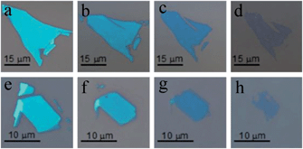 | ||
| Fig. 1 Optical microscopy images of the pristine (a, e), and thermal annealed MoS2 flakes (b–d) and (f–h). From (b) to (d), the annealing times are 2 hours, 4 hours and 7 hours. From (f) to (h), the annealing times are also 2 hours, 4 hours and 7 hours. | ||
Since thicker MoS2 flakes can reflect more light and show a brighter colour than thinner ones, the change of colour, from bright to dark, indicates that the flakes are getting thinner and thinner. Meanwhile, a shrinkage of the surface area is noticeable. This means that sublimation not only occurs perpendicularly on the surface, but also along the surface, thus resulting in smaller areas. To make a detailed comparison, we measured the contrast spectra of pristine single-layer to eight-layer MoS2 (Fig. 2b) and thinned MoS2 by thermal annealing (Fig. 2a), whose original number of layers was eight (shown in Fig. 1a).
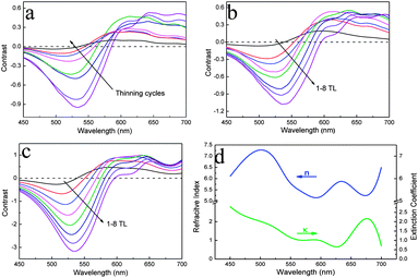 | ||
| Fig. 2 (a) Contrast spectra of the thermal thinning of MoS2. (b) Contrast spectra of pristine single- to eight-layer MoS2. (c) Contrast spectra from calculations. (d) Fitting refractive index n and extinction coefficient κ. | ||
From Fig. 2a and b, the vertical axis is the optical contrast C(λ), which is defined as:

R dark is the dark scan of the detector, and it can be treated as constant. If Rsample and Rsubstrate are much larger than Rdark, the above ratio would be much closer to Rsample/Rsubstrate, the relative reflectance that we are looking for. Therefore, it is reasonable that a smaller aperture size results in a smaller contrast than the true value. However, due to the limited size and irregular shape of the samples, we cannot use a larger aperture size, or it will be difficult to guarantee that the area within the aperture is of uniform thickness. Despite this, the good agreement between calculations and experiments (both pristine and thinned MoS2) shows that our results are robust.
To characterize the thinning process of the original seven-layer MoS2 sample (shown in Fig. 1d), we conducted a Raman scattering experiment. Compared to the high frequency regime, low frequency modes are much more sensitive to thickness.19 For instance, the B1 mode shifts from 10 cm−1 in a nine-layer sample to 40 cm−1 in a bilayer sample. However, the frequency difference between A1g and E12g increased from about 18 cm−1 in a monolayer sample to 24.5 cm−1 in a five-layer sample, which is already close to that from bulk. The original and thinned MoS2 flakes were measured after each cycle (one hour) under both parallel ![[z with combining macron]](https://www.rsc.org/images/entities/i_char_007a_0304.gif) (xx)z and cross (xy)z polarization configurations.19 From Fig. 3a, we can see that the low frequency breathing mode B1 peak shifts to a higher frequency and the shear mode E22g (called S1 for convenience) down shifts as the annealing cycle increases, indicating that the layer thickness is decreasing. The mixture of surfaces is also reflected in the spectra. The two B1 peaks after the second and third cycle of annealing confirm that the surface is a mixture of N and N − 1 layers (N = 6, 5) even in a small area, within a laser spot. After the seventh cycle, the interlayer breathing mode B1 and shear mode S1, which are mainly caused by van der Waals forces, disappear. The presence of the fingerprint modes A1g and E12g in Fig. 3b suggests that the sample is in monolayer regime. Meanwhile, the shifts in A1g and E12g, especially from the fourth cycle to the seventh cycle, are distinct. It can be regarded as another sign of thinning, which is in agreement with previous reports.14,16–19Fig. 3c and d are the spectra from the cross-polarized configuration. Only the shear mode vibration can be observed, since breathing modes, A1g and B1, are greatly suppressed. The down-shifted S1 in Fig. 3c is evidence of thinning. Two S1 peaks after the fourth and fifth cycle were observed, since the S1 peak shifts more in thinner MoS2 flake. This phenomenon indicates a mixed surface of N and N − 1 layers (N = 4, 3).
(xx)z and cross (xy)z polarization configurations.19 From Fig. 3a, we can see that the low frequency breathing mode B1 peak shifts to a higher frequency and the shear mode E22g (called S1 for convenience) down shifts as the annealing cycle increases, indicating that the layer thickness is decreasing. The mixture of surfaces is also reflected in the spectra. The two B1 peaks after the second and third cycle of annealing confirm that the surface is a mixture of N and N − 1 layers (N = 6, 5) even in a small area, within a laser spot. After the seventh cycle, the interlayer breathing mode B1 and shear mode S1, which are mainly caused by van der Waals forces, disappear. The presence of the fingerprint modes A1g and E12g in Fig. 3b suggests that the sample is in monolayer regime. Meanwhile, the shifts in A1g and E12g, especially from the fourth cycle to the seventh cycle, are distinct. It can be regarded as another sign of thinning, which is in agreement with previous reports.14,16–19Fig. 3c and d are the spectra from the cross-polarized configuration. Only the shear mode vibration can be observed, since breathing modes, A1g and B1, are greatly suppressed. The down-shifted S1 in Fig. 3c is evidence of thinning. Two S1 peaks after the fourth and fifth cycle were observed, since the S1 peak shifts more in thinner MoS2 flake. This phenomenon indicates a mixed surface of N and N − 1 layers (N = 4, 3).
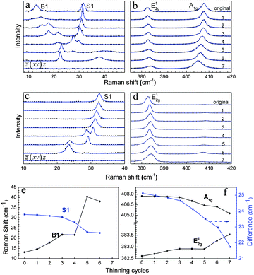 | ||
| Fig. 3
Raman spectra of a thinning MoS2 flake under (xx)z configuration at low frequency (a) and high frequency (b) regions. Raman spectra of a thinning MoS2 flake under (xy)z configuration at low frequency (c) and high frequency (d) regions. Raman shifts of S1, B1 (e) and A1g, E12g (f) of few-layer MoS2 as a function of thinning cycles. | ||
We summarize the shifts of the S1, B1, A1g and E12g modes as a function of the annealing cycles in Fig. 3e and f. The general trend of shifting confirms that thermal annealing can thin down few-layer MoS2. From Fig. 3d, we can see that after the sixth cycle, A1g was not as suppressed as in other cycles. We believe there may be some heat-induced disorders after this cycle, which mainly affect out-of-plane vibrations. Although the full width at half maximum (FWHM) of the pristine bilayer is comparably larger than of the other multilayers, it almost reaches 8.5 cm−1 after the sixth thinning cycle. For the rest of the thinning cycles, FWHM of the S1, B1, A1g and E12g peaks is below 2.0 cm−1, mostly around 1.5 cm−1 (data not shown here), which indicates that thermal annealing does not compromise the crystalline quality of few-layer MoS2 in terms of its optical properties. The frequency difference of A1g and E12g is about 21.5 cm−1 in a monolayer, and close to 23 cm−1 in a bilayer, which is larger than that of the pristine MoS2 produced by the mechanical exfoliated method.14 Similar effects were observed in monolayer MoS2 flakes fabricated by the chemical method12 and laser thinning.24 On the other hand, the smaller frequency difference in the monolayer (16 cm−1) and the bilayer (21 cm−1) was also noticed in mechanically exfoliated MoS2 in a previous report.23 Instead of the other likely reasons such as local thickness variation12 and a rougher surface caused by the laser,24 we believe this small difference is related to the lifetime of phonons. Similarly to laser thinning, we obtain a large frequency difference in thinned monolayers, as both thinning methods share a similar mechanism, a heat-induced sublimation. From our results, a larger frequency difference is mainly caused by the shear mode E12g, which did not shift too much after the fifth cycle. Therefore, we conclude that too many thermal thinning cycles will influence the force in shear mode vibration, while that of the breathing mode can hardly be affected.31
We further used AFM to check the uniformity and surface roughness of a thinned MoS2 flake. Fig. 4a shows a flat surface of an exfoliated MoS2 flake (the corresponding optical image is Fig. 1a), which is about 5.5 nm in thickness, corresponding to an eight-layer sample. After one annealing cycle, an inhomogeneous surface appears, indicating that some parts are getting thinned to six-layer flakes, while some parts are seven-layer flakes, as shown in Fig. 4b. In repeated experiments, although we have succeeded in thinning a small portion of samples to homogeneous thickness, for most atomically thin MoS2 flakes an inhomogeneous surface appears. We therefore considered vacancy defects as a possible reason to cause the uneven surface. The vacancy defects could come naturally from the samples themselves, as well as during the thinning process. In a “perfect” and “defect-free” MoS2 sample, sublimation can happen randomly in any area, leaving vacancies (thickness is N − 1 layers after sublimation), which make their surrounding parts (N layers) easier to sublimate due to the broken covalent bonds. As to the surface roughness, since there is inhomogeneity, we just selected some parts with uniform thickness and find that the roughness hardly changed during the thinning process, even when it came to the thinned bilayer and monolayer samples.
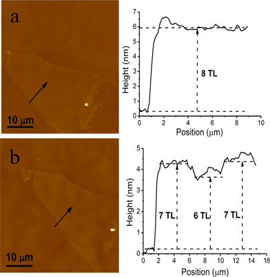 | ||
| Fig. 4 AFM images of a pristine eight-layer MoS2 (a) and thinned MoS2 after one cycle (b). | ||
Conclusion
To conclude, via thermal annealing, few-layer MoS2 flakes can be peeled off layer-by-layer. The thinning process was characterized by microspectrophotometry, Raman spectroscopy and AFM. During thinning, we can see that the crystalline quality does not change much, and the surface roughness mostly stays stable. Although the thinning process is not perfectly layer-by-layer yet, we believe that thinned MoS2 flakes with homogenous surfaces can be achieved by thermal annealing. Thus, we consider this easy and low-cost approach a promising top-down method for fabricating single- and few-layer MoS2, as well as facilitating future in situ measurements on electronic and optical properties. This thinning process may apply to other transition metal dichalcogenides as well.Acknowledgements
Q. X. acknowledges the strong support from the Singapore National Research Foundation through a Fellowship grant (NRF-RF2009-06), the Singapore Ministry of Education via two tier2 grants (MOE2011-T2-2-051 and MOE2012-T2-2-086) and the Nanyang Technological University via a start-up grant support (M58110061).Notes and references
- Q. H. Wang, K. Kalantar-Zadeh, A. Kis, J. N. Coleman and M. S. Strano, Nat. Nanotechnol., 2012, 7, 699–712 CrossRef CAS.
- K. F. Mak, C. Lee, J. Hone, J. Shan and T. F. Heinz, Phys. Rev. Lett., 2010, 105, 136805 CrossRef.
- B. Radisavljevic, A. Radenovic, J. Brivio, V. Giacometti and A. Kis, Nat. Nanotechnol., 2011, 6, 147–150 CrossRef CAS.
- B. Radisavljevic, M. B. Whitwick and A. Kis, Appl. Phys. Lett., 2012, 101, 043103 CrossRef.
- H. Li, Z. Y. Yin, Q. Y. He, X. Huang, G. Lu, D. W. H. Fam, A. I. Y. Tok, Q. Zhang and H. Zhang, Small, 2012, 8, 63–67 CrossRef CAS.
- H. Wang, L. L. Yu, Y. H. Lee, Y. M. Shi, A. Hsu, M. L. Chin, L. J. Li, M. Dubey, J. Kong and T. Palacios, Nano Lett., 2012, 12, 4674–4680 CrossRef CAS.
- T. Cao, G. Wang, W. P. Han, H. Q. Ye, C. R. Zhu, J. R. Shi, Q. Niu, P. H. Tan, E. Wang, B. L. Liu and J. Feng, Nat. Commun., 2012, 3, 887 CrossRef.
- K. F. Mak, K. L. He, J. Shan and T. F. Heinz, Nat. Nanotechnol., 2012, 7, 494–498 CrossRef CAS.
- H. L. Zeng, J. F. Dai, W. Yao, D. Xiao and X. D. Cui, Nat. Nanotechnol., 2012, 7, 490–493 CrossRef CAS.
- S. Tongay, J. Zhou, C. Ataca, K. Lo, T. S. Matthews, J. B. Li, J. C. Grossman and J. Q. Wu, Nano Lett., 2012, 12, 5576–5580 CrossRef CAS.
- K. F. Mak, K. He, C. Lee, G. H. Lee, J. Hone, T. F. Heinz and J. Shan, Nat. Mater., 2013, 12, 207–211 CrossRef CAS.
- G. Eda, H. Yamaguchi, D. Voiry, T. Fujita, M. Chen and M. Chhowalla, Nano Lett., 2011, 11, 5111–5116 CrossRef CAS.
- A. Splendiani, L. Sun, Y. B. Zhang, T. S. Li, J. Kim, C. Y. Chim, G. Galli and F. Wang, Nano Lett., 2010, 10, 1271–1275 CrossRef CAS.
- C. Lee, H. Yan, L. E. Brus, T. F. Heinz, J. Hone and S. Ryu, ACS Nano, 2010, 4, 2695–2700 CrossRef CAS.
- A. Molina-Sanchez and L. Wirtz, Phys. Rev. B, 2011, 84, 155413 CrossRef.
- S. L. Li, H. Miyazaki, H. Song, H. Kuramochi, S. Nakaharai and K. Tsukagoshi, ACS Nano, 2012, 6, 7381–7388 CrossRef.
- G. Plechinger, S. Heydrich, J. Eroms, D. Weiss, C. Schuller and T. Korn, Appl. Phys. Lett., 2012, 101, 101906 CrossRef.
- H. L. Zeng, B. R. Zhu, K. Liu, J. H. Fan, X. D. Cui and Q. M. Zhang, Phys. Rev. B, 2012, 86, 241301(R) Search PubMed.
- Y. Zhao, X. Luo, H. Li, J. Zhang, P. T. Araujo, C. K. Gan, J. Wu, H. Zhang, S. Y. Quek, M. S. Dresselhaus and Q. H. Xiong, Nano Lett., 2013, 13, 1007–1015 CrossRef CAS.
- J. N. Coleman, M. Lotya, A. O'Neill, S. D. Bergin, P. J. King, U. Khan, K. Young, A. Gaucher, S. De, R. J. Smith, I. V. Shvets, S. K. Arora, G. Stanton, H. Y. Kim, K. Lee, G. T. Kim, G. S. Duesberg, T. Hallam, J. J. Boland, J. J. Wang, J. F. Donegan, J. C. Grunlan, G. Moriarty, A. Shmeliov, R. J. Nicholls, J. M. Perkins, E. M. Grieveson, K. Theuwissen, D. W. McComb, P. D. Nellist and V. Nicolosi, Science, 2011, 331, 568–571 CrossRef CAS.
- R. J. Smith, P. J. King, M. Lotya, C. Wirtz, U. Khan, S. De, A. O'Neill, G. S. Duesberg, J. C. Grunlan, G. Moriarty, J. Chen, J. Z. Wang, A. I. Minett, V. Nicolosi and J. N. Coleman, Adv. Mater., 2011, 23, 3944–3948 CrossRef CAS.
- Y. C. Lin, W. J. Zhang, J. K. Huang, K. K. Liu, Y. H. Lee, C. T. Liang, C. W. Chu and L. J. Li, Nanoscale, 2012, 4, 6637–6641 RSC.
- K. K. Liu, W. J. Zhang, Y. H. Lee, Y. C. Lin, M. T. Chang, C. Su, C. S. Chang, H. Li, Y. M. Shi, H. Zhang, C. S. Lai and L. J. Li, Nano Lett., 2012, 12, 1538–1544 CrossRef CAS.
- A. Castellanos-Gomez, M. Barkelid, A. M. Goossens, V. E. Calado, H. S. van der Zant and G. A. Steele, Nano Lett., 2012, 12, 3187–3192 CrossRef CAS.
- K. Gacem, M. Boukhicha, Z. S. Chen and A. Shukla, Nanotechnology, 2012, 23, 505709 CrossRef.
- Y. Liu, H. Nan, X. Wu, W. Pan, W. Wang, J. Bai, W. Zhao, L. Sun, X. Wang and Z. Ni, ACS Nano, 2013, 7, 4202–4209 CrossRef CAS.
- M. M. Benameur, B. Radisavljevic, J. S. Heron, S. Sahoo, H. Berger and A. Kis, Nanotechnology, 2011, 22, 125706 CrossRef CAS.
- A. Castellanos-Gomez, N. Agrait and G. Rubio-Bollinger, Appl. Phys. Lett., 2010, 96, 213116 CrossRef.
- H. Li, G. Lu, Z. Y. Yin, Q. Y. He, Q. Zhang and H. Zhang, Small, 2012, 8, 682–686 CrossRef CAS.
- Z. H. Ni, H. M. Wang, J. Kasim, H. M. Fan, T. Yu, Y. H. Wu, Y. P. Feng and Z. X. Shen, Nano Lett., 2007, 7, 2758–2763 CrossRef CAS.
- J. Zhang, Z. P. Peng, A. Soni, Y. Y. Zhao, Y. Xiong, B. Peng, J. B. Wang, M. S. Dresselhaus and Q. H. Xiong, Nano Lett., 2011, 11, 2407–2414 CrossRef CAS.
| This journal is © The Royal Society of Chemistry 2013 |