
MOF-enabled high-density 2D molecular crystal optoelectronic memory transistor with floating gate architecture†
Shaosong
Gao‡
a,
Yiwen
Ren‡
a,
Dong
Zhang
b,
Xianshuo
Wu
a,
Yidi
Xie
a,
Lingjie
Sun
b,
Rongjin
Li
 a,
Fangxu
Yang
*a and
Wenping
Hu
a
a,
Fangxu
Yang
*a and
Wenping
Hu
a
aKey Laboratory of Organic Integrated Circuits, Ministry of Education & Tianjin Key Laboratory of Molecular Optoelectronic Sciences, Department of Chemistry, School of Science, Tianjin University, Tianjin 300072, China. E-mail: yangfangxu@tju.edu.cn
bKey Laboratory of Organic Integrated Circuits, Ministry of Education & Tianjin Key Laboratory of Molecular Optoelectronic Sciences, Department of Chemistry, Institute of Molecular Aggregation Science, Tianjin University, Tianjin 300072, China
First published on 17th April 2024
Abstract
Organic field-effect floating-gate transistors combine the advantages of organic semiconductor materials to produce more functionality by sensing changes in photogenerated carriers, allowing data to be stored efficiently. Herein, a novel metal–organic framework (MOF) floating gate optical memory transistor was engineered using a two-dimensional molecular crystal (2DMC) as the active layer via a layer-by-layer assembly technique. Highly uniform ultra-thin MOF films were synthesized at the gas–liquid interface and subsequently transferred to serve as the floating gate layer. The device exhibited a substantial memory window of 36 V upon optical pulse stimulation and maintained its performance without degradation after 100 cycles of optical programming and electrical erasure testing, demonstrating exceptional durability. Moreover, it displayed remarkable current-holding characteristics about 10![[thin space (1/6-em)]](https://www.rsc.org/images/entities/char_2009.gif) 000 seconds under varying light intensities and achieved multi-level memory functionality with significant current differences. These findings substantiate its potential commercial viability in high-performance information memory devices.
000 seconds under varying light intensities and achieved multi-level memory functionality with significant current differences. These findings substantiate its potential commercial viability in high-performance information memory devices.
 Fangxu Yang | Fangxu Yang obtained his master's degree from Harbin Institute of Technology in 2009 and his PhD from the Institute of Chemistry, Chinese Academy of Sciences in 2016 under the supervision of Professor Wenping Hu. Afterward, he engaged in postdoctoral research at Tianjin University and joined the faculty in 2019. He has since been appointed as a professor at Tianjin University. His research interests lie in the field of photoelectric detection and imaging using organic semiconductor crystals, with a particular focus on high-energy radiation, near-infrared, and terahertz. |
1. Introduction
With the advent of the internet of things (IoT) era, the utilization of intelligent devices has led to a substantial accumulation of data information, consequently elevating the demand for enhanced memory capacity.1,2 Therefore, it is imperative to develop memory devices with augmented storage capabilities, robust retention, and multifunctionality.3–5 Benefiting from the designability and flexibility of organic semiconductor materials, organic memory devices have garnered widespread attention and development to meet the ever-growing demand for high storage density.6–9 Among various types of devices, field-effect floating gate transistor memories are promising due to their ability to preserve charge-trapping centers within the device, preventing slow release of charges and thus achieving robust storage capabilities.10–13 Moreover, unlike traditional electrically programmable memory devices that read information, field-effect floating gate transistors involve a charge-trapping layer that can form an additional control electric field by capturing photogenerated carriers, providing a degree of freedom in the optical control of storage capabilities.14–18 In this manner, a single device can be employed to achieve multi-level memory with significant current differences by harnessing adjustable light intensity.19 Additionally, utilizing light to control the programming process in transistor memories also offers the advantages of low power consumption and high sensitivity.20 Therefore, the development of innovative floating gate memory devices with both excellent storage capabilities and multi-bit abilities lays the groundwork for high density memory applications.The ability of materials in the floating gate layer to sequester electrons or holes is crucial for the efficiency of the memory device.21,22 In previous studies, perovskite materials,23,24 metal oxides,25,26 and two-dimensional materials27–30 were employed as charge-trapping materials. To achieve high-performance memory applications, it is necessary to continue developing new floating gate materials capable of capturing charges generated by photons or through field effects. Two-dimensional metal–organic framework (2D MOF) thin films, formed by coordination structures through transition metal ions and planar conjugated aromatic ligands, are poised to emerge as charge-trapping materials.31–34 By employing MOF thin films as floating gate layers, their intrinsic porosity, high surface area, and tailorable processing attributes can preserve captured electrons within the MOF thin films over an extended period. Furthermore, the presence of MOF thin films can facilitate the efficient separation of photogenerated excitons in the channel, resulting in significant charge transfer effects and enabling photocontrolled storage capabilities. Therefore, the utilization of MOF thin films as charge-trapping materials in floating gate memory holds substantial significance.35–37 Concurrently, organic semiconductor materials possess unique optoelectronic properties, while two-dimensional molecular crystals (2DMCs) with single crystal and ultra-thin thickness have been identified as the most promising candidate materials for optoelectronic transistors.38–40 The ultra-thin thickness of 2DMCs can surmount the interlayer shielding effect, resulting in ultra-low dark-state currents, which can facilitate multilevel memory with substantial current differentiation.41 Additionally, 2DMCs exhibit rapid response to photons, and their ultra-thin thickness can also promote the effective separation of interface photogenerated excitons.40 Consequently, the use of MOF thin films as charge-trapping layers and 2DMCs as photosensitive active layers opens up a new development idea for constructing high-performance, multi-level floating-gate transistor memories.
Herein, we synthesized high-quality, uniformly continuous ultra-thin MOF films using a gas–liquid interface method for the floating gate charge-trapping layer. Subsequently, a blocking layer PMMA was spin-coated on its top, followed by the transfer of 2DMCs, thereby constructing a MOF floating gate optical memory transistor. The devices can display a memory window of 36 V under light pulse stimulation. 100 cycles of optical programming and electrical erasure testing showed no performance degradation. Under stimulation of different light intensities, a multi-level memory function with large current differences was achieved, with a maximum current difference of more than three orders of magnitude, and demonstrated good current retention characteristics (about 10000 s). The capture and release processes of photogenerated carriers have been studied by using Kelvin probe force microscope (KPFM) and photoluminescence (PL) spectra. Finally, the T-shape was successfully displayed on a 3 × 3 phototransistor array and was capable of being sustained for an extended period.
2. Results and discussion
2.1 Preparation and characterization of 2D MOF films
Fig. 1a shows a schematic diagram of the synthesis of two-dimensional Cu3(HHTP)2 MOF membranes through a gas–liquid interface method. In interface synthesis, by adding organic ligand solution dropwise above the metal ion aqueous solution, the organic ligand solution will expand and self-assemble on the surface of the aqueous solution to form MOF films. The solvent choice for the organic ligand solution is crucial, which impacts the solvation ability and the spreading state at the interface. The film growth in several different solvents was compared (as shown in Fig. S1–S3, ESI†). The smooth and continuous growth of MOF films can be achieved by using ethyl acetate (EA) and methyl benzene (MB) as solvents and adding appropriate amounts of dimethyl sulfoxide (DMSO). A centimeter-scale film without any cracks can be obtained and transferred onto the Si/SiO2 substrate, as shown in Fig. 1b. Optical microscopy (OM) and scanning electron microscopy (SEM) confirmed the uniform flatness of the Cu3(HHTP)2 thin films over a large area (Fig. 1c and d). The atomic force microscopy (AFM) image of the 2D Cu3(HHTP)2 film is shown in Fig. S4 (ESI†). By measuring the roughness and thickness of the MOF film at six different sites, the surface of the MOF film is homogeneous, and the thickness of the MOF film is uniform. As shown in Fig. 1e, the Cu3(HHTP)2 film was observed to have a good crystalline state through transmission electron microscopy (TEM). Meanwhile, a lattice spacing of 1.8 nm was obtained by high-resolution transmission electron microscopy (HRTEM), as depicted in Fig. 1f. The hexagonal lattice structure was displayed using fast Fourier transform (FFT) (Fig. S5, ESI†), which is consistent with previously reported literature.42,43 As shown in Fig. 1g, the crystal structure of MOF thin films was further characterized by X-ray diffraction (XRD), and the diffraction peaks of 2θ = 4.7°, 9.5°, 12.6°, and 27.7° correspond to (100), (200), (210), and (002), respectively.44,45 FT-IR spectra show that metal ions were successfully coordinated with organic ligands,37 as shown in Fig. S6 (ESI†). As shown in Fig. 1h and i and Fig. S7 (ESI†), X-ray photoelectron spectroscopy (XPS) shows the formation and high coordination of Cu, C, and O elements in MOF films, consistent with literature reports.45 Thus, high quality MOF films were successfully prepared here, ready for subsequent use in floating gate layers.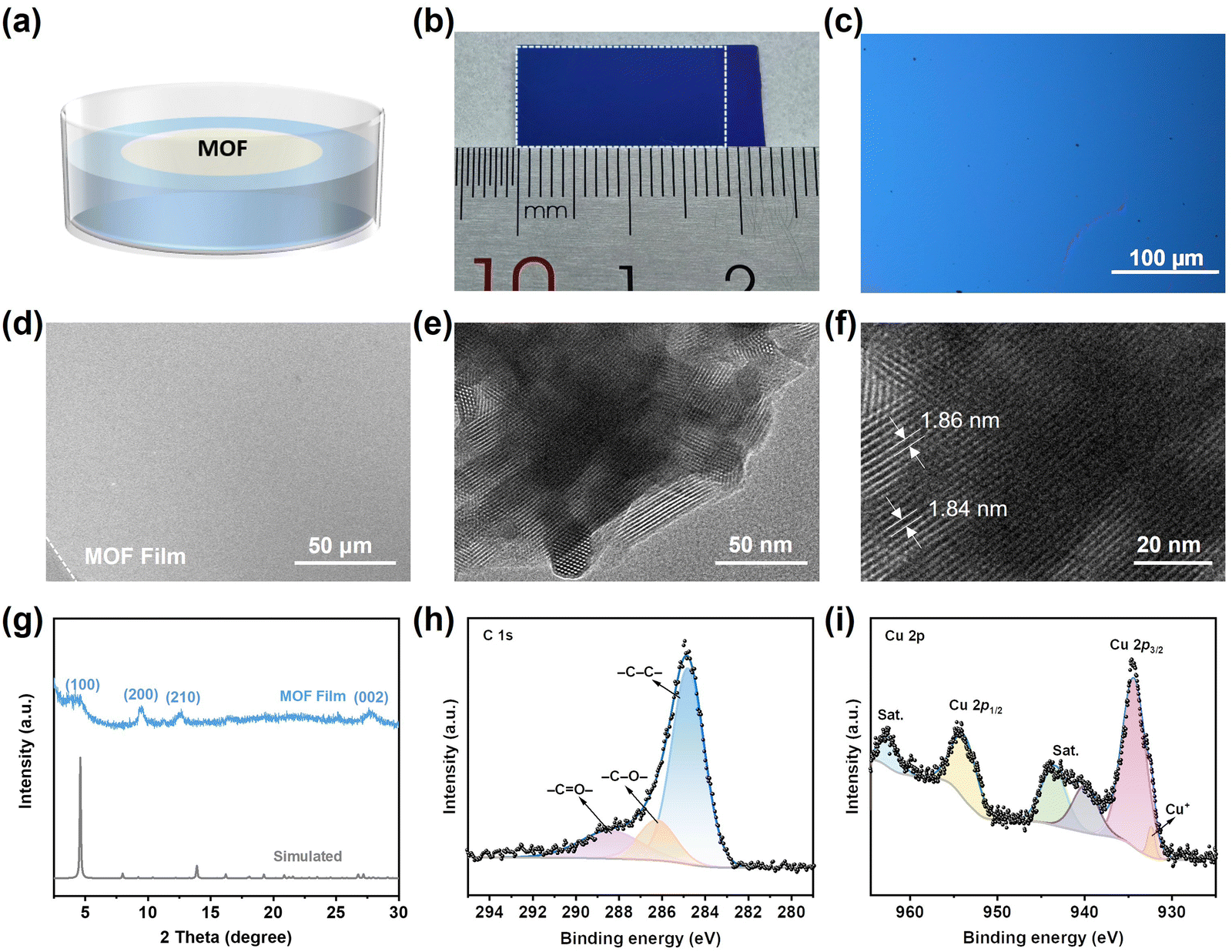 | ||
| Fig. 1 (a) A schematic diagram of the synthesis of two-dimensional Cu3(HHTP)2 MOF film through a gas–liquid interface method. (b) Photograph of 2D MOF film on a SiO2/Si substrate. (c) Optical image of Cu3(HHTP)2 MOF film. (d) SEM image of Cu3(HHTP)2 MOF film. (e) and (f) HRTEM images of Cu3(HHTP)2 MOF film. (g) XRD pattern of Cu3(HHTP)2 MOF film. (h) High resolution C 1s XPS spectra of Cu3(HHTP)2 film. (i) High resolution Cu 2p XPS spectra of Cu3(HHTP)2 film. | ||
2.2 Preparation and characterization of 2DMCs
As another pivotal component, high-quality two-dimensional molecular crystals (2DMCs) were employed as the channel layer in floating-gate optical memory transistors. Due to its exceptional charge transport capabilities and photoelectric response, 2,6-bis(4-octylphenyl)-dithieno[3,2-b:2′,3′-d]thiophene (DTT-8) was chosen as the channel material. A large-area single crystal film of DTT-8 with long ordered arrangement can be grown using a well-developed “solution epitaxy” method.46 To be specific, a mixture of DTT-8 and surfactant solution was dispensed onto the surface of glycerol, which functioned as a viscous liquid matrix. This not only restricted the movement of the organic solution but also eradicated the coffee ring effect by preventing triple-phase line pinning. Furthermore, the surfactant significantly reduces the surface tension of the solution, facilitating its spread across the glycerol surface, which consequently leads to the successful assembly of millimeter-sized, high-quality 2DMCs.The optical microscope image of DTT-8 is shown in Fig. 2a, with a uniform and smooth surface, uniform morphology, and large area. As shown in Fig. 2b and c, under the observation of a polarized optical microscope, when the entire sample is rotated 45°, the color of DTT-8 undergoes a uniform change from dark to bright, indicating that the sample has high crystallinity. The single crystal properties of DTT-8 were confirmed through bright field transmission electron microscopy (TEM) images and selected area electron diffraction (SAED) patterns, as shown in Fig. 2d and e. In the TEM image, the surface of DTT-8 exhibits a continuous, smooth, and uniform morphology at the nanoscale. In the SAED mode of DTT-8, the diffraction points are arranged in a bright and regular pattern. The lattice parameters of the crystal obtained through calculation are consistent with those reported in the literature.18 The X-ray diffraction (XRD) mode of DTT-8 is shown in Fig. S8 (ESI†). In the spectrum, the sharp diffraction peak of DTT-8 indicates that the prepared 2DMCs have high crystal quality. According to the single crystal data reported in previous literature,18 the diffraction peaks of DTT-8 at 2.5°, 5.0°, and 7.5° can be divided into (200), (400), and (600) diffraction peaks, respectively. This indicates that the bc-plane of 2DMC is parallel to the substrate. The atomic force microscopy (AFM) image of DTT-8 2DMC is shown in Fig. 2f. From this image it can be seen that the surface of DTT-8 2DMC is smooth and flat, with a surface roughness of 0.45 nm in the selected area, indicating its atomic level flatness. The thickness of the DTT-8 2DMC is 10.5 nm. The UV-vis absorption spectra was tested to characterize the optical properties of DTT-8 2DMC, as shown in Fig. S9 (ESI†). It can be seen from the figure that DTT-8 2DMC exhibits a significant absorption peak at 365 nm. Therefore, a 365 nm laser will subsequently be employed to examine its photoelectric properties.
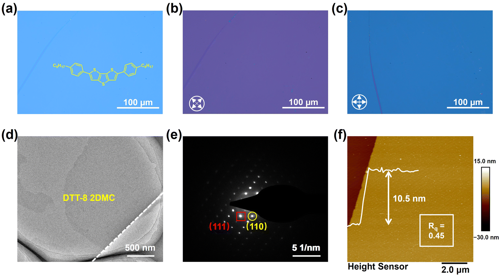 | ||
| Fig. 2 (a) Optical microscope (OM) image of DTT-8 2DMC. (b) and (c) POM image of DTT-8 2DMC. (d) TEM image of DTT-8 2DMC. (e) The corresponding SAED patterns of DTT-8 2DMC. (f) AFM image of DTT-8 2DMC. | ||
2.3 2DMC optical memory transistors based on MOF floating gate
Floating-gate optical memory transistors are constructed by preparing and transferring high-quality MOF films for use in a floating-gate layer and using 2DMCs as the active layer. The device preparation process is shown in Fig. S10 (ESI†). First, the prepared MOF film was transferred onto the Si/SiO2 (300 nm) substrate. Then, the surface of the MOF film was spin-coated with PMMA solution (as shown in Fig. S10, ESI†). The PMMA can not only act as a barrier layer, but also provide a hydrophobic surface to facilitate the subsequent transfer of 2DMCs. Next, the grown 2DMCs were transferred to the surface of PMMA. Finally, Au (120 nm) was selected as the source and drain electrode, and attached to the surface of DTT-8 2DMC using a mechanical transfer method. As shown in Fig. 3a, a bottom-gate top-contact organic field-effect transistor (OFET) device with a floating-gate structure was constructed. The OFET device based on DTT-8 2DMC exhibits significant p-type transport characteristics, with its transfer and output curves shown in Fig. S11 (ESI†).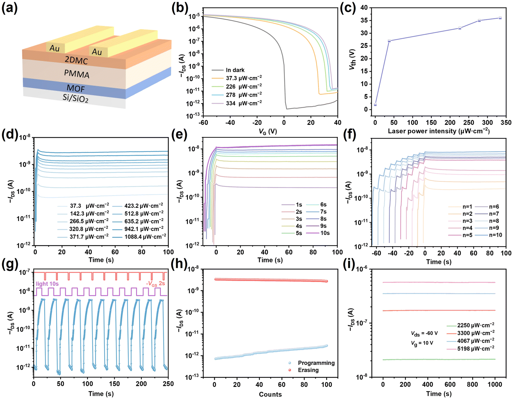 | ||
| Fig. 3 (a) The organic field-effect floating-gate transistor device. (b) Different light intensity characteristics of a floating gate transistor based on DTT-8 2DMC under 365 nm laser irradiation. (c) Shift of Vth as a function of laser power intensity. (d) Ten different current states by changing different light intensities. (e) Ten different current states by changing the illumination time. (f) Ten different current states by changing the pulse illumination numbers. (g) The typical programming/erasing (P/E) cycle process of the device. (h) The current level of the memory after 100 cycles of programming/erasing. (i) The current level after 1000 seconds. | ||
The light response characteristics of a floating gate transistor based on DTT-8 2DMC were studied under different light intensities of 365 nm laser irradiation (Fig. 3b). As shown in Fig. 3c, under 365 nm light irradiation, the transfer curve moves in the positive direction, and the threshold voltage undergoes a positive shift. The maximum threshold voltage shift is 36 V. Under the irradiation of ultraviolet light, the source–drain current (IDS) increases and the threshold voltage undergoes a significant positive shift, which is mainly due to the combination effect of photogating effect and photoconductivity effect. Photosensitivity (P), responsivity (R) and specific detectivity (D*) at different gate voltages (VGS) and illumination intensities were measured as an important parameter for evaluating phototransistors, as shown in Fig. S12 (ESI†). Under light irradiation, the maximum P value is 1 × 10⁷, the R value is 450 A W−1, and the D* value is 7 × 10¹⁵ Jones.
The excellent performance of phototransistors comes from the strong gate control ability of 2DMCs, which can completely deplete charge carriers and obtain extremely low dark state currents. This superior photo response performance lays the foundation for obtaining high-performance optical memory transistors. Interestingly, after laser irradiation, the IDS state of the device remains unchanged (as shown in Fig. 3d), that is, the high conductivity state in the channel remains unchanged, resulting in a persistent photoconductivity effect. Fig. 3d shows the relationship of IDS with different light intensities. After laser irradiation, IDS increased by up to 3 orders of magnitude, and the change in IDS became larger with the increase of light intensity. By changing different light intensities, ten different current states can be obtained. In addition, ten different current states can be obtained by changing the illumination time (Fig. 3e) and pulse illumination numbers (Fig. 3f). As shown in Fig. S13 (ESI†), by testing the transfer curves of the MOF/PMMA/DTT-8 and PMMA/DTT-8 devices, as well as the curves at different illumination numbers and intensities, the results showed that the behavior of the optical switch could only be shown in the absence of the MOF film, without memory behavior. It can be proved that MOF film, as a floating gate layer, can capture photogenerated electrons, which makes it difficult for electrons to recombine after being captured, as shown in Fig. S14 (ESI†). By combining these methods of changing light dose, different current states can be obtained in the optical memory transistor, achieving the function of multi-level memory. The implementation of this function benefits from two aspects: (1) 2DMCs have a very sensitive response to light, which enables them to regulate their conductivity state through different doses of light. (2) The gate control ability of 2DMCs is strong, which can achieve a very large light–dark current switching ratio, providing a basis for obtaining different current states. Thus, different current states can be clearly distinguished. Optoelectronic memory not only requires the process of optical programming, but also needs to be erased. Fig. 3g shows the typical programming/erasing (P/E) cycle process of the device. The process of programming the illumination using a 365 nm laser for 10 seconds resulted in a very high level of current. Subsequently, the negative gate voltage (VGS = −60 V) was applied for 2 seconds to erase it and restore its current to its initial state. Fig. 3h shows the change in current level of the memory after 100 cycles of programming/erasing. The high conductivity state in the programming state shows almost no attenuation, while the low conductivity state in the erasing state slightly increases, proving that our memory has excellent optical programming/electrical erasing cycle characteristics. The memory still exhibits excellent current retention characteristics after optical programming, and after 1000 seconds, there is no attenuation in the current level (Fig. 3i). The optical memory floating gate transistor can achieve a retention time of up to approximately 10000 seconds, demonstrating excellent memory functionality, as shown in Fig. S15 (ESI†). With the increase of light intensity, a higher on/off ratio of 2 × 10⁶ can be achieved, as shown in Fig. S16 (ESI†).
2.4 Working mechanism of optical memory transistors
In order to further understand the process of optoelectronic programming and erasure that this device can achieve, we have explained the working mechanism of the device. Firstly, the surface potential changes of 2DMC with the MOF floating gate structure before and after laser irradiation were characterized using KPFM, as shown in Fig. 4a. After laser irradiation (lasting for 20 seconds), the surface potential of DTT-8 2DMC increased significantly. The color change of the surface potential in Fig. 4b was very obvious, changing from dark to bright. The surface potential increased from 823 mV to 1162 mV, as shown in Fig. 4d. This result indicates that after absorbing photons, the concentration of charge carriers in 2DMC increases, leading to an increase in its surface potential. The KPFM measurement results are consistent with the trend of the transfer curve, with electrons captured and Vth experiencing a positive shift (Fig. 3b). And after the light is removed, there is no significant decrease in the surface potential of 2DMC, indicating that electrons are permanently captured. After ten minutes, the surface potential of 2DMC was scanned again, but there was still no downward trend. The surface color remained basically consistent with the color after illumination, and there was no significant change in surface potential. As shown in Fig. 4c, this is consistent with the experimental results mentioned above. After illumination, the channel can maintain a high conductivity state without significant attenuation. Steady state PL measurements can be used to study charge transfer efficiency, and to further confirm 2DMC underwent a significant charge transfer process after illumination. We tested the PL spectra of the MOF/PMMA/DTT-8 structure and PMMA/DTT-8 structure (Fig. 4e), and it was evident from the comparison that the PL intensity of DTT-8 molecules decreased after the addition of MOF film. This can be attributed to the effective separation of photo generated excitons at the PMMA/MOF interface by DTT-8, resulting in a decrease in the PL intensity of DTT-8. In addition, the dual exponential function can be used to match the PL decay dynamics of DTT-8/PMMA/MOF and DTT-8/PMMA to obtain their PL lifetime parameters (Fig. 4f). The results indicate the fast component of PL lifetime parameters for DTT-8/PMMA/MOF thin films (τ1) and the slow components (τ2). The values are 1.71 ns and 7.71 ns respectively, both of which are smaller than those of DTT-8/PMMA thin films τ1 (1.91 ns) and τ2 (9.39 ns). The shorter PL lifetime parameters of DTT-8/PMMA/MOF indicate that the presence of MOF accelerates the separation of DTT-8 photogenerated excitons.16,17 | ||
| Fig. 4 (a) Schematic diagram of the surface potential of an optical memory transistor studied using KPFM mode. (b) Surface potential changes of DTT-8 2DMC before and after laser irradiation. (c) The surface potential after ten minutes of laser irradiation. (d) The change of surface potential of DTT-8 2DMC after laser irradiation. (e) The PL spectra of the MOF/PMMA/DTT-8 structure and PMMA/DTT-8 structure. (f) The PL lifetime parameters of the MOF/PMMA/DTT-8 structure and PMMA/DTT-8 structure. (g) Under the initial state, (h) during the optical programming operation, and (i) during the electrical erasing operation. | ||
Based on the above research process, this operating mechanism has been obtained. The energy band diagram under initial, optical programming, and electrical erasure conditions is shown in Fig. 4g–i and Fig. S17 (ESI†). Under optical programming conditions, a large number of photo generated electron hole pairs will be generated in DTT-8 2DMC. Due to band bending, the photo generated electrons in DTT-8 can easily transfer to the LUMO level of the MOF, while the photo generated holes remain in the HOMO level of DTT-8, achieving a high conductivity state.37 After removing the light, the presence of PMMA blocks the electron return to DTT-8 in the MOF, and the metal ions in the MOF film can very easily bind electrons, allowing the captured electrons to remain in the MOF for a long time. However, when applying negative gate voltage erasure, the energy band of DTT-8 bends downwards, and the accumulated holes generated by photocurrent can easily transfer to the HOMO level of the MOF and recombine with the captured photogenerated electrons. At the same time, the number of holes on the DTT-8 HOMO level decreases, restoring the original conductivity level. We implemented a reciprocating cycle process of optical programming and electrical erasure.
2.5 Image sensing and memory function based on optical memory transistors
To further demonstrate the potential application prospects of the obtained transistor memories, we showcased their imaging storage function. Initially, a 35 × 35 μm2 square gold electrode was evaporated onto a large area of DTT-8 2DMC surface to serve as the source and drain electrodes, with a channel length of 30 μm between adjacent electrodes. As shown in Fig. 5b, a 3 × 3 pixel photo-memory transistor array was fabricated. This array is capable of encoding the geometric shape of an object through the heatmap representation of the array's current magnitude, effectively achieving imaging. Upon exposure to laser light, the IDS increased from 10−12 A to greater than 10−8 A, and after removing the light laser irradiation for 30 minutes, there was no significant attenuation in the current level (Fig. 5c), indicating that our device has excellent memory function. Consequently, a T-shaped hollow mask was placed on top of the 3 × 3 pixel photo-memory transistor array, creating a current mapping image by projecting the T-shape optical pattern onto the device array (Fig. 5a). The current level in the hollowed-out area exposed to light is greater than10−8 A, while the current in the area blocked by the mask is 10−12 A, with a current difference of more than four orders of magnitude. As shown in Fig. 5d–f, the T-shape pattern is clearly visible after illumination. Based on the outstanding information memory function, there was no significant change in the current level after 30 minutes, and a T-shaped graph was still displayed. This successfully demonstrated the potential application of our devices in image storage.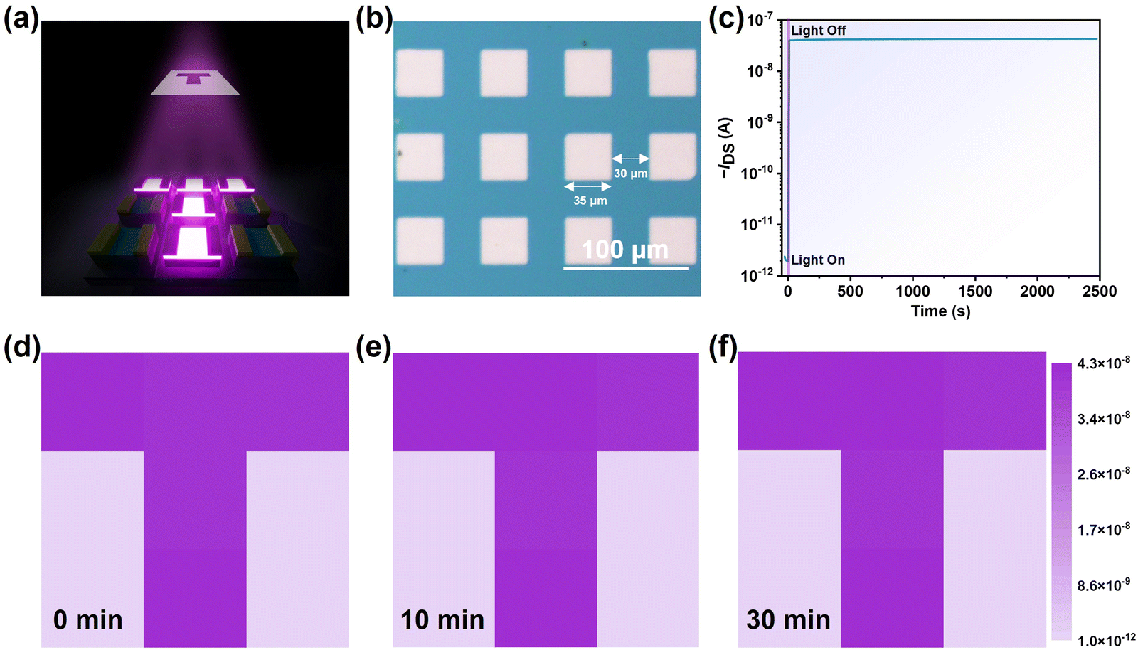 | ||
| Fig. 5 (a) Schematic diagram of a transistor array. (b) The 3 × 3 pixel transistor array. (c) The retention time of optical memory transistors. (d)–(f) 3 × 3 optical memory transistor array current mapping images at 0, 10, and 30 minutes after laser irradiation. | ||
3. Conclusions
In summary, we synthesized smooth and uniform MOF thin films using an interface method as floating gate capture materials for organic field-effect transistor memory devices, and demonstrated their excellent photo generated carrier capture ability. A MOF floating gate optical memory transistor was constructed using layer-by-layer assembly technology, combining 2DMC as the active layer. Floating gate optical memory transistors display a memory window of 36 V under photon stimulation. They have a stable memory performance and can efficiently capture electrons even after 100 cycles of optical programming and electrical erasure testing. Under the stimulation of different light intensities, a multi-level memory function with a large current difference was achieved, and the maximum current difference was more than three orders of magnitude, demonstrating a current retention characteristic of about 10000 seconds. It has also achieved the display of a T-shape pattern on an array of optoelectronic transistors for 30 minutes. By utilizing the excellent charge-trapping ability of MOF thin films and the photogenerated carrier sensing effects of 2DMCs, the developed high-density optical memory transistors show promising potential for future applications.
4. Experimental section
Materials
2,3,6,7,10,11-Hexahydroxytriphenylene hydrate was purchased from Aladdin. Copper(II) acetate monohydrate (C4H6CuO4·H2O) was purchased from Aladdin. 2,6-Bis(4-octylphenyl)-dithieno[3,2-b:2′,3′-d]thiophene (DTT-8) was purchased from Lumtec. Poly(methylmethacrylate) (PMMA) (Mw ≈ 12000) was purchased from Aladdin. All materials were used without purification.
Preparation of 2D MOF films
2D MOF thin films were prepared using a gas–liquid interface method. Disperse 10 mg of copper acetate monohydrate into 100 mL of deionized water. Disperse 1 mg of HHTP powder into 10 mL of a mixed solvent (EA:MB:DMSO = 8:1:1), and sonicate for 30 minutes at 50 Hz to obtain a uniform solution. Then slowly drop the HHTP solution onto the aqueous solution to allow metal ions and organic ligands to self-assemble on the water surface to form MOF film. Finally, it can be transferred to the substrate for testing and characterization.
Preparation of 2DMC
25 mL of glycerol was poured into the weighing flask as a liquid substrate for 2DMC growth. Then, 50 μL of the prepared DTT-8 solution (1 mg mL−1 in chlorobenzene) was measured with a pipette gun and slowly dripped onto the glycerol surface, which was placed in an atmospheric environment at 16 °C. After the chlorobenzene solvent slowly evaporated completely, DTT-8 2DMC was obtained on the glycerol surface.Device fabrication
SiO2 (300 nm)/Si wafers as the substrate were ultrasonically cleaned with deionised water, acetone and isopropanol separately for 10 min, followed by oxygen plasma treatment. The substrate was used to transfer the MOF film. PMMA solution (10 mg mL−1 in chlorobenzene) was spin-coated onto the MOF film and annealed at 120 °C for 30 min. After that, the substrate was inverted over the 2DMC grown on the glycerol surface so that the crystals adhered to the surface of the substrate, after which the substrate was fished out with tweezers and the glycerol on the surface of the 2DMC was rinsed with deionised water. The device with a bottom-gate/top-contact (BGTC) configuration was prepared by stamping two pieces of Au (120 nm thickness) electrodes onto the 2DMC as the source and drain electrodes.Instrumentation and characterization
Polarized optical microscope (POM) images were obtained using a Nikon ECLIPSE Ci-POL. TEM and SAED patterns were obtained using a Tecnai G2 F20 S-TWIN. AFM and KPFM images were obtained using a Bruker Dimension Icon in air. The X-ray photoelectron spectroscopy (XPS) results were obtained using a Thermo ESCALAB 250XI X-ray photoelectron spectrometer with Al kα ray. PL measurements were carried out using a HITACHI Florescence Spectrophotometer F-7000 with 365 nm laser excitation. XRD was conducted using a Rigaku SmartLab X-ray diffractometer with the highest power of 9 kW (step size 0.01°). The UV-vis-NIR absorption spectrum was obtained by Cary 7000. The optoelectronic properties were determined using a 365 nm laser generator with tunable power from 0.008 to 3.6 mW cm−2. The OFET and memory measurements were carried out using a semiconductor parameter analyzer (Keithley B2912A) in the air and at room temperature.Author contributions
S. Gao and Y. Ren contributed equally to this work. L. Sun, R. Li, F. Yang, and W. Hu conceived the idea and directed the project. S. Gao synthesized 2D MOF films and characterized their morphology and structure. Y. Ren prepared 2DMC and measured the electrical properties of OFET. D. Zhang characterized 2DMC. X. Wu analyzed the working mechanism. Y. Xie performed imaging characterization. All authors have analyzed and discussed the experimental results.Conflicts of interest
There are no conflicts to declare.Acknowledgements
The authors thank the National Key R&D Program (2022YFB3607500), the National Natural Science Foundation of China (No. 52373194) and the open research fund from State Key Laboratory of Luminescent Materials and Devices (2023-skllmd-02).References
- Z. Chen, S. Chen, T. Jiang, S. Chen, R. Jia, Y. Xiao, J. Pan, J. Jie and X. Zhang, Nanoscale, 2024, 16, 3721–3728 RSC
.
- F. Zhang, M. Shao, C. Wang, W. Wen, W. Shi, M. Qin, H. Huang, X. Wei, Y. Guo and Y. Liu, Adv. Mater., 2023, 36, 2307326 CrossRef PubMed
- F. Yang, L. Sun, Q. Duan, H. Dong, Z. Jing, Y. Yang, R. Li, X. Zhang, W. Hu and L. Chua, SmartMat, 2021, 2, 99–108 CrossRef CAS
- S. K. Hwang, I. Bae, R. H. Kim and C. Park, Adv. Mater., 2012, 24, 5910–5914 CrossRef CAS PubMed
- J. Y. Chen, Y. C. Chiu, Y. T. Li, C. C. Chueh and W. C. Chen, Adv. Mater., 2017, 29, 1702217 CrossRef PubMed
- C. Ma, Z. Luo, W. Huang, L. Zhao, Q. Chen, Y. Lin, X. Liu, Z. Chen, C. Liu, H. Sun, X. Jin, Y. Yin and X. Li, Nat. Commun., 2020, 11, 1439 CrossRef CAS PubMed
- S. H. Yu, S. Z. Hassan, C. So, M. Kang and D. S. Chung, Adv. Mater., 2022, 35, 2203401 CrossRef PubMed
- J. Y. Chen, H. Wang, H. Chen, W. Zhang, S. Xu, M. Pätzel, C. Ma, C. Wang, I. McCulloch, S. Hecht and P. Samorì, Adv. Funct. Mater., 2023, 33, 2305494 CrossRef
- Y. Kim, C. Zhu, W. Y. Lee, A. Smith, H. Ma, X. Li, D. Son, N. Matsuhisa, J. Kim, W. G. Bae, S. H. Cho, M. G. Kim, T. Kurosawa, T. Katsumata, J. W. F. To, J. Y. Oh, S. Paik, S. J. Kim, L. Jin, F. Yan, J. B. H. Tok and Z. Bao, Adv. Mater., 2022, 35, 2203541 CrossRef PubMed
- M. L. M. Lalieu, R. Lavrijsen and B. Koopmans, Nat. Commun., 2019, 10, 110 CrossRef CAS PubMed
- L. Shao, Y. Zhao and Y. Liu, Adv. Funct. Mater., 2021, 31, 2101951 CrossRef CAS
- M. D. Tran, H. Kim, J. S. Kim, M. H. Doan, T. K. Chau, Q. A. Vu, J. H. Kim and Y. H. Lee, Adv. Mater., 2018, 31, 1807075 CrossRef PubMed
- Y. C. Chiang, C. C. Hung, Y. C. Lin, Y. C. Chiu, T. Isono, T. Satoh and W. C. Chen, Adv. Mater., 2020, 32, 2002638 CrossRef CAS PubMed
- H. Shao, Y. Li, J. Chen, W. Yang, L. Wang, J. Fu, Y. Wang, H. Ling, L. Xie and W. Huang, SmartMat, 2023, 4, 1–11 Search PubMed
- X. Zhu, Y. Yan, L. Sun, Y. Ren, Y. Zhang, Y. Liu, X. Zhang, R. Li, H. Chen, J. Wu, F. Yang and W. Hu, Adv. Mater., 2022, 34, 2201364 CrossRef CAS PubMed
- J. Zhang, Z. Guo, T. Sun, P. Guo, X. Liu, H. Gao, S. Dai, L. Xiong and J. Huang, SmartMat, 2023, 4, 1–14 Search PubMed
- J. Zhang, P. Guo, Z. Guo, L. Li, T. Sun, D. Liu, L. Tian, G. Zu, L. Xiong, J. Zhang and J. Huang, Adv. Funct. Mater., 2023, 33, 2302885 CrossRef CAS
- X. Zhu, C. Gao, Y. Ren, X. Zhang, E. Li, C. Wang, F. Yang, J. Wu, W. Hu and H. Chen, Adv. Mater., 2023, 35, 2301468 CrossRef CAS PubMed
- B. Yang, Y. Lu, D. Jiang, Z. Li, Y. Zeng, S. Zhang, Y. Ye, Z. Liu, Q. Ou, Y. Wang, S. Dai, Y. Yi and J. Huang, Adv. Mater., 2020, 32, 2001227 CrossRef CAS PubMed
- M. Carroli, A. G. Dixon, M. Herder, E. Pavlica, S. Hecht, G. Bratina, E. Orgiu and P. Samorì, Adv. Mater., 2021, 33, 2007965 CrossRef CAS PubMed
- Y. Yu, Q. Ma, H. Ling, W. Li, R. Ju, L. Bian, N. Shi, Y. Qian, M. Yi, L. Xie and W. Huang, Adv. Funct. Mater., 2019, 29, 1904602 CrossRef CAS
- N. Shi, J. Zhang, Z. Ding, H. Jiang, Y. Yan, D. Gu, W. Li, M. Yi, F. Huang, S. Chen, L. Xie, Y. Ren, Y. Li and W. Huang, Adv. Funct. Mater., 2021, 32, 2110784 CrossRef
- W. Lin, G. Chen, E. Li, L. He, W. Yu, G. Peng, H. Chen and T. Guo, ACS Appl. Mater. Interfaces, 2020, 12, 43967–43975 CrossRef CAS PubMed
- H. Lai, Y. Zhou, H. Zhou, N. Zhang, X. Ding, P. Liu, X. Wang and W. Xie, Adv. Mater., 2022, 34, 2110278 CrossRef CAS PubMed
- X. Liu, H. Zhao, G. Dong, L. Duan, D. Li, L. Wang and Y. Qiu, ACS Appl. Mater. Interfaces, 2014, 6, 8337–8344 CrossRef CAS PubMed
- J. Pei, X. Wu, W.-J. Liu, D. W. Zhang and S.-J. Ding, ACS Nano, 2022, 16, 2442–2451 CrossRef CAS PubMed
- Y. Zhai, X. Yang, F. Wang, Z. Li, G. Ding, Z. Qiu, Y. Wang, Y. Zhou and S. T. Han, Adv. Mater., 2018, 30, 1803563 CrossRef PubMed
- H. Qiu, Z. Liu, Y. Yao, M. Herder, S. Hecht and P. Samorì, Adv. Mater., 2020, 32, 1907903 CrossRef CAS PubMed
- D. Xiang, T. Liu, J. Xu, J. Y. Tan, Z. Hu, B. Lei, Y. Zheng, J. Wu, A. H. C. Neto, L. Liu and W. Chen, Nat. Commun., 2018, 9, 2966 CrossRef PubMed
- X. Yang, J. Yu, J. Zhao, Y. Chen, G. Gao, Y. Wang, Q. Sun and Z. L. Wang, Adv. Funct. Mater., 2020, 30, 2002506 CrossRef CAS
- K. W. Nam, S. S. Park, R. dos Reis, V. P. Dravid, H. Kim, C. A. Mirkin and J. F. Stoddart, Nat. Commun., 2019, 10, 4948 CrossRef PubMed
- J.-H. Dou, M. Q. Arguilla, Y. Luo, J. Li, W. Zhang, L. Sun, J. L. Mancuso, L. Yang, T. Chen, L. R. Parent, G. Skorupskii, N. J. Libretto, C. Sun, M. C. Yang, P. V. Dip, E. J. Brignole, J. T. Miller, J. Kong, C. H. Hendon, J. Sun and M. Dincă, Nat. Mater., 2020, 20, 222–228 CrossRef PubMed
- T. C. Narayan, T. Miyakai, S. Seki and M. Dincă, J. Am. Chem. Soc., 2012, 134, 12932–12935 CrossRef CAS PubMed
- G. Wu, J. Huang, Y. Zang, J. He and G. Xu, J. Am. Chem. Soc., 2016, 139, 1360–1363 CrossRef PubMed
- H. Arora, R. Dong, T. Venanzi, J. Zscharschuch, H. Schneider, M. Helm, X. Feng, E. Cánovas and A. Erbe, Adv. Mater., 2020, 32, 1907063 CrossRef CAS PubMed
- C. K. Liu, V. Piradi, J. Song, Z. Wang, L. W. Wong, E. H. L. Tan, J. Zhao, X. Zhu and F. Yan, Adv. Mater., 2022, 34, 2204140 CrossRef CAS PubMed
- X. Song, X. Wang, Y. Li, C. Zheng, B. Zhang, C. a Di, F. Li, C. Jin, W. Mi, L. Chen and W. Hu, Angew. Chem., Int. Ed., 2019, 59, 1118–1123 CrossRef PubMed
- F. Yang, S. Cheng, X. Zhang, X. Ren, R. Li, H. Dong and W. Hu, Adv. Mater., 2018, 30, 1702415 CrossRef PubMed
- F. Yang, L. Jin, L. Sun, X. Ren, X. Duan, H. Cheng, Y. Xu, X. Zhang, Z. Lai, W. Chen, H. Dong and W. Hu, Adv. Mater., 2018, 30, 1801891 CrossRef PubMed
- B. Fu, F. Yang, L. Sun, Q. Zhao, D. Ji, Y. Sun, X. Zhang and W. Hu, Adv. Mater., 2022, 34, 2203330 CrossRef CAS PubMed
- L. Zhang, X. Tian, J. Yao, X. Song, S. Yang, S. Guo, Y. Wang, B. Li, X. Ren, Y. Sun, F. Yang, R. Li and W. Hu, J. Mater. Chem. C, 2021, 9, 8834–8841 RSC
- Z.-Z. Ma, Q.-H. Li, Z. Wang, Z.-G. Gu and J. Zhang, Nat. Commun., 2022, 13, 2203330 Search PubMed
- M. Hmadeh, Z. Lu, Z. Liu, F. Gándara, H. Furukawa, S. Wan, V. Augustyn, R. Chang, L. Liao, F. Zhou, E. Perre, V. Ozolins, K. Suenaga, X. Duan, B. Dunn, Y. Yamamto, O. Terasaki and O. M. Yaghi, Chem. Mater., 2012, 24, 3511–3513 CrossRef CAS
- K. Yuan, T. Song, C. Yang, J. Guo, Q. Sun, Y. Zou, F. Jiao, L. Li, X. Zhang, H. Dong, L. Li and W. Hu, J. Am. Chem. Soc., 2021, 143, 17526–17534 CrossRef CAS PubMed
- Y. Liu, Y. Wei, M. Liu, Y. Bai, X. Wang, S. Shang, J. Chen and Y. Liu, Angew. Chem., Int. Ed., 2020, 60, 2887–2891 CrossRef PubMed
- J. Yao, Y. Zhang, X. Tian, X. Zhang, H. Zhao, X. Zhang, J. Jie, X. Wang, R. Li and W. Hu, Angew. Chem., Int. Ed., 2019, 58, 16082–16086 CrossRef CAS PubMed
Footnotes |
| † Electronic supplementary information (ESI) available. See DOI: https://doi.org/10.1039/d4tc00421c |
| ‡ These authors contributed equally to this work. |
| This journal is © The Royal Society of Chemistry 2024 |