 Open Access Article
Spiers Memorial Lecture: Challenges and prospects in organic photonics and electronics
Michele
Catacchio
 a,
Mariapia
Caputo
 a,
Lucia
Sarcina
 b,
Cecilia
Scandurra
 b,
Angelo
Tricase
 a,
Verdiana
Marchianò
 a,
Eleonora
Macchia
 a,
Paolo
Bollella
 *b and
Luisa
Torsi
 *b
*b
aDipartimento di Farmacia-Scienze del Farmaco, Università degli Studi di Bari “Aldo Moro”, 70125 Bari, Italy
bDipartimento di Chimica and Centre for Colloid and Surface Science, Università degli Studi di Bari Aldo Moro, 70125 Bari, Italy. E-mail: luisa.torsi@uniba.it
First published on 21st February 2024
Abstract
While a substantial amount of research activity has been conducted in fields related to organic photonics and electronics, including the development of devices such as organic field-effect transistors, organic photovoltaics, and organic light-emitting diodes for applications encompassing organic thermoelectrics, organic batteries, excitonic organic materials for photochemical and optoelectronic applications, and organic thermoelectrics, this perspective review will primarily concentrate on the emerging and rapidly expanding domain of organic bioelectronics and neuromorphics. Here we present the most recent research findings on organic transistors capable of sensing biological biomarkers down at the single-molecule level (i.e., oncoproteins, genomes, etc.) for the early diagnosis of pathological states and to mimic biological synapses, paving the way to neuromorphic applications that surpass the limitations of the traditional von Neumann computing architecture. Both organic bioelectronics and neuromorphics exhibit several challenges but will revolutionize human life, considering the development of artificial synapses to counteract neurodegenerative disorders and the development of ultrasensitive biosensors for the early diagnosis of cancer to prevent its development. Moreover, organic bioelectronics for sensing applications have also triggered the development of several wearable, flexible and stretchable biodevices for continuous biomarker monitoring.
1. Introduction
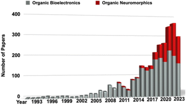
Bioelectronics is a discipline dating back to the pioneering experiments conducted by Luigi Galvani during the 18th century. In his renowned studies, he demonstrated the twitching of detached frog legs by applying a minute electric voltage. Presently, the field of bioelectronics has evolved significantly, giving rise to a diverse range of devices.1,2 These advanced bioelectronic devices not only enhance healthcare practices but also contribute to environmental preservation and expedite scientific advancements. Despite the great interest devoted to organic photonics and electronics, most of the researchers are currently focusing on organic bioelectronics and neuromorphics, as emerging technologies (Fig. 1).3,4In this regard, many organic materials have been customized (e.g., by adding functional groups, changing rheological features, etc.) to obtain specific electronic, photonic, and chemical properties and design organic bioelectronics. This paves the way for the development of bioelectronic devices and systems characterized by the essential attributes of flexibility, elasticity, and variable morphology. Additionally, these devices boast a surface chemistry that promotes biocompatibility and ensures long-term stability. Organic electronic materials are capable of efficiently conducting and processing both electronic and ionic (bio)signals, effectively bridging the gap between electronic and ionic charge compensation.5
Organic bioelectronics is a field of research and development dedicated to creating organic electronic devices that bridge the gap between signals and functions in biological systems and those in human-made electronic processing systems. In one direction, this technology allows precise control over the physiology of cells, tissues, and organs in a specific chemical manner, maintaining high spatiotemporal accuracy. Conversely, it can be integrated into biological systems to selectively detect, record, and monitor a variety of signals and physiological conditions. Additionally, it can convert gathered parameters into electronic data for further analysis and decision-making processes. This reciprocal connection between biology and electronics holds significant potential for diverse applications in healthcare, biotechnology, and beyond.6,7
Organic neuromorphics, also known as organic synaptic electronics, have gained widespread attention globally due to their numerous advantages. These include the wide availability of materials, cost-effectiveness, suitability for mass production, low operational voltage, physical flexibility, and compatibility with flexible substrates. These organic synaptic devices have significant potential not only in energy-efficient computing systems utilizing neural network algorithms, but also in the development of future flexible neuromorphic systems for highly efficient signal processing.8
One notable application involves the development of bio-inspired electronic skin (e-skin) for robots, which demands a substantial number of mechanoreceptors, thermoreceptors, and nociceptors. This leads to a rapid increase in sensory data, posing a significant challenge in managing these extensive input signals from sensor-integrated intelligent systems. The adoption of hardware-based neuromorphic processing, utilizing architectures resembling neural networks, can be invaluable in addressing this challenge.9,10
Organic artificial synapses (organic neuromorphics) show significant promise for future applications in adaptable intelligent systems. These applications include flexible electronic skins, interfaces between humans and machines, and pliable robotic systems. They will affect various fields like robotics and human–computer interaction.8
This review discusses the most recent research findings on organic bioelectronics (Section 2) and organic transistors capable of mimicking biological synapses (Section 3), paving the way for neuromorphic applications that overcome the limitations of the traditional von Neumann computing architecture, and sensing biological biomarkers down at the single-molecule level (i.e., in oncoproteins, genomes, etc.) for the early diagnosis of pathological states, or even controlling ionic-biochemical cell signalling (Section 4). All technologies exhibit several challenges but will revolutionize human life considering the development of artificial synapses to counteract neurodegenerative disorders, and the development of ultrasensitive biosensors for the early diagnosis of cancer to prevent its onset. Moreover, organic bioelectronics for sensing applications have also triggered the development of several wearable, flexible and stretchable biodevices for continuous biomarker monitoring (Section 5). Finally, Section 6 draws some conclusions and provides future perspectives within the field.
2. Emerging organic bioelectronics: challenges and applications
Over the past decades, organic bioelectronics have been widely used in biological research and medical science.7 Organic bioelectronics are built upon conductive polymers, inheriting their advantageous properties, such as flexibility, optical transparency, electrical conductivity, and ionic conductivity. Furthermore, the adaptability and functionalization of these materials using organic chemistry techniques make them highly versatile, particularly well-suited for medical applications, allowing for precise modelling of various aspects of cellular and human tissue attributes. The direct integration of electronic devices with living organisms occurs at multiple levels, including organs, tissues, cells, cell membranes, proteins, and small biomolecules. Once electronic materials establish a connection with biological entities, the devices can initiate the process of detecting biological signals and translating them into electronic outputs, effectively functioning as sensors. Alternatively, they can administer electronic charges and/or dispense biochemical molecules to actively intervene in biological processes, operating as actuators.11,12Among all electronic materials, organic semiconductors (OSs) have been widely explored to fabricate either organic field-effect transistors (OFETs) or organic electrochemical transistors (OECTs).3
Organic semiconductors (OSs) consist of organic molecules or polymers with a planar structure and π electrons. π electrons create electronic density above and below the molecule. Key in OSs are the highest occupied molecular orbital (HOMO) and lowest unoccupied molecular orbital (LUMO), characterized by the π electron distribution. Adjacent OS molecules interact weakly (π–π interactions), affecting optical properties, exciton size, and transport features, including charge mobility and the transport gap. Crystalline OS structures have narrow conduction bands influenced by LUMO–HOMO interactions, impacting optical properties, oxidation/reduction potentials, reactivity, and electronic transport.13–17
Narrow electronic bands (<0.2 eV) involve localized charge carriers moving through temperature-activated hopping (0.01–0.1 cm2 V−1 s−1). Wider bands result in delocalized charge carriers across multiple molecules (10–50 cm2 V−1 s−1). Some disordered semiconducting polymers show local order, ensuring moderate mobility (around 1 cm2 V−1 s−1). OSs can capture, store, and transmit energy for a range of electronic applications, from individual molecules to textiles, spanning various length scales.18–20 These materials have been used for a number of single-molecule sensing electronic applications.21–28
Besides OSs, organic mixed ionic electronic conductors (OMIECs) are widely employed in creating transistors, sensors, energy-storage devices, and more. They possess a conjugated backbone for electronic conduction and sidechains that aid in ion intercalation and solvent processing. The combination of electronic and ionic conduction, along with solvation capabilities, makes OMIECs valuable for flexible and efficient electronic devices.29–31
Changes in OMIECs’ properties result from significant alterations in electronic and ionic charge density within the material. This leads to various effects, impacting properties like electrochemical potential, transportation of electrons and ions, capacitance, optical bandgap, and modulus. OMIECs allow precise property adjustments within the bulk material, unlike traditional devices where modulation typically occurs only at interfaces.32 For instance, OMIECs can achieve substantial volumetric capacitances, enhancing transconductance in transistors. They also improve the permeability of chemical species throughout the bulk, benefiting sensors and fuel cells without complex electrode nanostructuring. OMIECs’ unique tunability within a single material has driven extensive research in designing and synthesizing novel OMIECs. These materials find applications in various devices, including electrochromic displays, organic electrochemical transistors, neuromorphic transistors, bioelectronic devices, and actuators. Some of these technologies are nearing commercialization, underlining the importance of bridging the gap between molecular design, device physics, and manufacturing processes.33
Considering all the mentioned materials, organic bioelectronics offer the potential for biosensing with incredibly precise spatiotemporal resolution. These state-of-the-art technologies have primarily been applied in the biomedical field.7 In contrast, in plant science, traditional sensing methods have relied on invasive techniques involving tissue sampling. This approach restricts in vivo detection and often results in limited spatiotemporal resolution, which hinders the understanding of dynamic biochemical processes in plants. The incorporation of bioelectronic devices into plant research has the potential to transform the field by enabling non-invasive, real-time, and high-resolution monitoring of biochemical activities within live plants.34 This development holds the promise of significantly improving our comprehension of plant physiology and how plants respond to various stimuli.
In a study by Stavrinidou and colleagues, implantable sensors based on OECTs were introduced for real-time monitoring of glucose and sucrose levels in plants (depicted in Fig. 2a and b). These sensors enabled in vivo monitoring, offering researchers unprecedented insights into plant biological processes.35
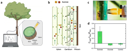 | ||
| Fig. 2 (a) The OECT was inserted into the xylem tissue, as illustrated in the diagram; (b) the process of sucrose transport in the vascular tissues; (c) photo of the OECT device within a poplar stem; and (d) selectivity of sucrose detection. Reproduced from ref. 34 with permission of the American Chemical Society. | ||
As a proof-of-concept, the technology was used to explore previously unexamined diurnal fluctuations in sucrose levels within the xylem sap of greenhouse-grown hybrid aspen (Populus tremula x tremuloides). OECT-based sensors were placed in the plant stem, specifically in the mature xylem tissue. These sensors continuously collected data over a 48 hour period (Fig. 2c). The results revealed significant diurnal patterns in sucrose concentration within the xylem tissue, increasing at night and decreasing during the day. In contrast, glucose levels remained relatively constant throughout the monitoring period (Fig. 2d). Control devices, used for comparison, showed no significant changes, underscoring the OECT sensors’ specificity and effectiveness in capturing these dynamic plant physiological changes. This data provides valuable insights into plant circadian rhythms and metabolic processes.
This discovery not only underscores the capabilities of OECT-based sensors but also emphasizes the fresh biological knowledge that can be acquired by using them. The capacity to acquire real-time, non-invasive data marks a notable progression in plant research, enabling a more profound comprehension of plant physiology and responses.
In carnivorous plants like the Venus flytrap (VFT; Dionaea muscipula), when mechanosensitive cells, such as sensory hairs, are stimulated, they trigger rapid electrical changes referred to as action potentials (APs).36 These APs are usually associated with quick plant movements and are a significant aspect of plant physiology. Stavrinidou and her team have created a flexible multi-electrode array (MEA) using organic electronics, designed for large-scale and high-resolution plant electrophysiology. Using this innovative technology, they could accurately chart the time- and space-based patterns of APs within the VFT. They demonstrated that APs actively spread through the plant tissue during both non-closure and closure-inducing events, which are linked to trap movement. This advanced electrophysiology setup enabled them to identify the source of spontaneously generated APs.
The authors developed the NeuroGrid probe, which covers a wide area, measuring 20 mm by 25 mm. It comprises 120 evenly spaced conducting polymer-based electrodes, each measuring 500 μm by 500 μm, as illustrated in Fig. 3a. The NeuroGrid’s flexibility is crucial for capturing electrophysiological data effectively, even on the curved surface of the Venus flytrap (VFT) in both open and closed states, as demonstrated in Fig. 3b. To observe the propagation of action potentials (APs) within the VFT, the NeuroGrid was delicately attached to the trap lobe’s outer surface, avoiding mechanical stimulation of sensitive hairs, as shown in Fig. 3c. A small amount of electrolyte was applied between the recording electrodes and the plant tissue.
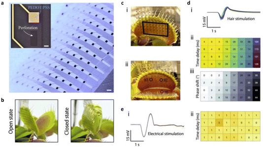 | ||
| Fig. 3 (a) The images display the NeuroGrid MEA, where electrodes are spaced 2 mm apart. The main image includes a 1 mm scale bar, while the inset focuses on a 500 μm by 500 μm PEDOT:PSS/Au electrode with a 250 μm scale bar; (b) the NeuroGrid is flexible and adapts to the VFT trap’s curvature in both open and closed states; (c) the NeuroGrid is attached to the outer side of a VFT lobe using an electrolyte. Active recording electrodes are denoted by black squares (i). Three hairs, H1, H3, and H6, are positioned relative to the NeuroGrid (ii); (d) mechanical stimulation of H1 results in the recording of generated action potentials (APs) (i). Analyzing time delays at each electrode allows the creation of a spatiotemporal propagation map (ii). This map’s accuracy is confirmed through phase-shift analysis (iii); (e) conversely, electrical stimulation of the trap from an external source (i) does not result in any signal propagation in the stimulation artifact (ii). Reproduced from ref. 34 with permission of the American Chemical Society. | ||
Stimulating a mechanosensitive hair led to the generation of an AP, meticulously tracked as it travelled through the trap lobe, detailed in Fig. 3di. Recorded data showed a noticeable time delay between different electrodes, confirming the setup’s essential spatial and temporal resolution for mapping signal propagation. This time delay data was used to create a map illustrating AP propagation, as seen in Fig. 3dii. Additionally, a thorough analysis of signal waveforms’ phase shifts provided further validation, confirming that the AP travelled without losing its frequency content, as shown in Fig. 3diii.
To investigate whether the recorded time delay was due to volume conduction (signal spreading through the electrolyte) or active signal propagation through plant tissue, researchers conducted an experiment. They applied an electrical stimulus to the Venus flytrap using an external electrode and recorded the response with the NeuroGrid, as depicted in Fig. 3ei. In this scenario, no significant time delay or phase shift was observed, indicating that electrical stimulation did not propagate but was simultaneously captured by all electrodes due to the high ionic conductivity of the epidermal tissue, confirmed in Fig. 3eii.
However, the observed time delay and phase shift during AP propagation suggested that APs travel through compartmentalized pathways within plant tissue, actively propagating without significant signal attenuation.
In the same context, a multiparameter stretchable sensor was designed to monitor various environmental parameters in plants while minimizing its impact on plant physiology. The sensor described in the study represents a remarkable integration of cutting-edge technologies, including CMOS, printable electronics, and transfer-printing techniques (Fig. 4a and b).37 This integration enables the sensor to have multifaceted capabilities for monitoring plants. The sensor incorporates meshed structures, which are arrangements of interconnected lines or patterns that resemble a mesh or grid. These structures are strategically designed and positioned within the sensor to optimize its performance. Meshed structures play a critical role in ensuring even strain distribution within the sensor’s ultrathin composition materials when the sensor is stretched. The meshed structures form an island–bridge configuration. In this setup, certain areas (the islands) are connected by thin lines or bridges. This configuration allows for controlled flexibility and stretchability of the sensor. The design of these island–bridge structures can be engineered to distribute strain evenly within the ultrathin materials when the sensor undergoes stretching. The serpentine interconnects are designed with secondary hierarchy structures. Such structures offer an additional level of stretchability and flexibility. They enable the entire sensor to conform to the growth and movement of the host leaf.
 | ||
| Fig. 4 (a) The OECT system includes components for monitoring relative humidity, temperature, strain, and light exposure; (b) the images show the system printed on Scindapsus aureus leaves immediately upon installation and after 7 days, highlighting its durability; (c) the system effectively monitors indoor environmental conditions for 2 days, showcasing the capabilities of this innovative wearable plant platform. Reproduced from ref. 34 with permission of the American Chemical Society. | ||
The sensor was tested on golden pothos (Scindapsus aureus) in a controlled environment. The environmental conditions were intentionally manipulated to assess the sensor’s performance over a one-week period. During the experiment, a range of external conditions were intentionally introduced to assess the sensor’s response. These conditions included wind blowing, cooling, water spraying, fog generation, and changes in light conditions (Fig. 4c). The results of the experiment demonstrated the sensor’s ability to provide timely and accurate responses to various stimuli. The sensor exhibited excellent responsiveness to changes in temperature. The system exhibited rapid responsiveness, promptly detecting and reacting to various external conditions that led to swift temperature fluctuations, some as substantial as 4.9 °C, in the local environment. Additionally, the sensor was capable of monitoring gradual temperature variations caused by natural conditions, such as a slow temperature change of 5.4 °C over the course of a day. The sensor’s temperature measurement element demonstrated a high level of sensitivity, with a temperature sensing resolution of 0.2 °C. The findings illustrated that the sensor’s ability to monitor environmental parameters was on par with that of commercially available devices. In a proof-of-concept trial, the sensor was further utilized in an outdoor environment, attached to a corn plant, and successfully tracked the plant’s microclimate over a duration of 2 hours. This experiment showcased the potential for real-world applications of such wearable sensors for plants in agricultural and environmental monitoring.
In agriculture, the integration of comprehensive technology that encompasses the collection of plant microclimate parameters along with plant physiological data, along with mechanisms for regulating plant physiology, has the potential to usher in a new era of intelligent and precise farming. With the rapid progress in big data analysis and the assistance of artificial intelligence, one can expect a fully automated agricultural process (as illustrated in Fig. 5). Nonetheless, there are several substantial challenges that must be confronted before achieving this level of sophistication.
 | ||
| Fig. 5 Turning our gaze towards the future, the left panel offers a glimpse of a fully integrated bioelectronic technology designed for smart agriculture. This cutting-edge technology fosters a seamless synergy among sensing, actuation, and decision-making, facilitated through a network of dispersed devices, cloud computing, and artificial intelligence. The ultimate objective is to optimize resource utilization and elevate crop yields in agriculture. In the right panel, we catch a sneak-peek into a visionary urban landscape where biohybrid plants take centre stage, symbolizing the potential for a more sustainable way of life. These biohybrids elegantly merge with the urban environment, coexisting harmoniously with the bustling city life. This futuristic vision alludes to the possibilities of a more interconnected and environmentally conscious urban existence. Reproduced from ref. 34 with permission of the American Chemical Society. | ||
The widespread integration of bioelectronic devices into numerous plants initially poses challenges in terms of cost and labour. However, the emergence of robotics provides an avenue for automating the integration process. Alternatively, a selective approach involves integrating the technology into specific indicator plants, which can serve as prototypes for optimizing the growth of a larger plant population.
A significant hurdle involves translating sensor data into actionable insights for farmers. Extensive research is necessary to pinpoint essential parameters of plant physiology that directly impact both product quality and growth optimization. Moreover, in real-world agricultural applications, a holistic technology solution is vital, covering aspects from power supply to data collection and transmission.
In the realm of basic research, concerns such as high costs and intricate protocols might not be significant. However, transitioning this technology into agriculture demands a focus on cost-effectiveness, scalability, user-friendliness, and precision. These factors are essential prerequisites for successfully commercializing bioelectronic products in the agricultural sector.
Organic bioelectronics, besides their sensing applications, also show promise as smart drug delivery systems. One notable innovation in this field is organic electronic ion pumps (OEIPs), which harness the electronic and ionic properties of organic materials. This unique combination allows precise release of ionic-biochemical signals for various biological purposes through electronic control. OEIPs function as “iontronic” resistors, facilitating the electrophoretic movement of charged substances across a cation- or anion-exchange membrane (AEM).38 This method enables incredibly accurate spatiotemporal delivery and dosage control, even down to delivering a single electron per monovalent ion. All OEIPs rely on ionically conducting polymers, or polyelectrolytes (PEs), which are vital for selective transport and precise delivery of ionic substances. The high fixed charge concentration on the polyelectrolyte membrane ensures selectivity in ionic transport, and the membrane’s polarity determines the direction and polarity of effectively transported charges.
Achieving the objectives of iontronics demands devices and materials that meet the complex demands of biological settings. This requires continuous progress in developing iontronic components with sophisticated, small-scale designs, and their seamless integration with compatible technologies. However, a notable drawback in the current production of iontronic PE membranes is their dependency on cleanroom techniques.39
Conventional microfabrication methods, although offering precise feature resolution, have limitations. They must align with strict processing and material requirements, such as high-temperature curing and chemical compatibility between different layers. Additionally, they demand substrates and materials that can withstand harsh processing conditions. Consequently, these microfabrication conditions can restrict the potential shapes and types of OEIP technologies, including substrate geometry. In research settings, these methods often involve multiple sequential steps that can result in significant material wastage, especially when using specialized materials produced in limited quantities for research purposes.40
To overcome these limitations in PE membrane microfabrication, a promising approach is the use of inkjet printing. Ultimately, the adoption of inkjet printing for PE membranes broadens the horizons for device designs and applications in iontronics research and development, offering enhanced flexibility and efficiency.
In their study, Simon and his colleagues explored the effectiveness of hyperbranched polyglycerol (HPG) membranes in delivering the pharmaceutical compound bupivacaine, which has a molecular weight of 343 g mol−1. They developed an in vitro protocol utilizing inkjet-based Organic Electronic Ion Pumps (inkjet-OEIPs) to achieve precise delivery of bupivacaine to live dorsal root ganglion (DRG) neurons (see Fig. 6).39 Bupivacaine is a nerve-blocking analgesic known for its reversible binding to sodium channels, preventing depolarization and subsequent nerve signalling downstream.
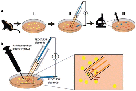 | ||
| Fig. 6 The in vitro experimental configuration involved the following procedures: (a) general guidelines: (i) dorsal root ganglia (DRGs) were initially obtained from a naive mouse and then subjected to dissociation to generate cultured cells (shown in yellow). (ii) The administration of bupivacaine to these cells was achieved using the Inkjet Organic Electronic Ion Pump (IJ-OEIP), resulting in the cells absorbing the bupivacaine (indicated in orange). (iii) Following this, potassium ions (K+) were introduced to the cells, and the ensuing fluorescence response was documented via a confocal microscope. Comparative analysis was performed using a control dish to gauge the consequences of bupivacaine delivery (cells that did not sufficiently bind bupivacaine are depicted in green, signifying a lack of significant reduction in subsequent calcium (Ca2+) activation); (b) detailed description of the in-dish setup: a Hamilton syringe was strategically positioned in proximity to the bupivacaine delivery point facilitated by the IJ-OEIP. A close-up inspection clearly delineates the trajectory of bupivacaine delivery, with precise orientation toward the cells (indicated by the red arrows). This setup ensured the meticulous and controlled administration of bupivacaine to the cells, streamlining subsequent experimental procedures and analysis. Reproduced from ref. 39 with permission of Wiley. | ||
DRG neurons loaded with a fluorescent calcium indicator were used to assess the effects of bupivacaine delivery. Changes in intracellular calcium (Ca2+) levels caused by potassium chloride (KCl) administration were monitored. KCl induces DRG depolarization by increasing extracellular potassium ions (K+) and subsequently opening sodium (Na+) and calcium (Ca2+) channels. Bupivacaine counteracts this by binding to sodium channels, preventing Na+ influx and membrane depolarization.
To confirm successful bupivacaine delivery through the Organic Electronic Ion Pump (OEIP), reduced activation of DRG neurons was expected after subsequent KCl administration, indicated by a smaller increase in intracellular calcium (Ca2+) levels. To ensure precise delivery, the OEIP outlets were directed downward toward the cells, enabling bupivacaine to be administered directly in the direction of the cells (as shown by the red arrows in Fig. 6).
Significant advancements have been made in comprehending the pathophysiology, treatment strategies, and molecular targets for various nervous system disorders. Many treatments involve monitoring and stimulating neural activity by electrical means, which has led to substantial efforts to enhance neural electrodes. Nonetheless, direct electrical connections have inherent constraints, such as the incapability to differentiate between various nerve-cell types. As a result, there is an increasing need for inventive tools that can accurately engage with nerve cells.
Richter-Dahlfors and her team have demonstrated the capability of an organic electronic device to accurately deliver neurotransmitters, both in laboratory settings and in living organisms.41 This device effectively mimics the function of a nerve synapse by converting electronic commands into neurotransmitter delivery. Through experiments conducted in the peripheral auditory system, the scientists have demonstrated that their device can specifically stimulate nerve cells that are sensitive to a particular neurotransmitter among a variety of different cells. This specificity is attained by carefully controlling electrophoretic motion within a polymer film through electronic means.
This process offers numerous desired characteristics for managing cell communication: it allows for precise dosage determination through electrochemical relationships, delivers neurotransmitters with minimal disturbance due to the absence of fluid flow, and offers the ability to be toggled on and off. This technology holds great promise as a therapeutic platform and has the potential to expedite the development of treatment approaches for nervous system disorders, offering hope for the future of neurology and neurotherapy.
In a similar application, the capillary organic electronic ion pump (c-OEIP) demonstrated remarkable penetration capabilities when applied to intact tobacco plants.42 Notably, it accomplishes this without triggering a significant wound response, as assessed over a 24 hour period. Moreover, this innovative device effectively transports the plant hormone abscisic acid (ABA) into the leaf apoplast. This OEIP-mediated delivery of ABA is especially noteworthy, since ABA is a phytohormone responsible for regulating a plant’s stress tolerance. When the c-OEIP administers ABA, it triggers the shutdown of stomata, the minute openings present in the epidermis of plant leaves. This closure of stomata is critical for processes like photosynthesis and transpiration, highlighting how this bioelectronic tool can potentially impact and improve a plant’s reaction to environmental challenges.
Using natural materials to create edible electronic devices is a promising innovation for improving point-of-care testing. These devices, which can be consumed as pills or integrated into food, are designed to work within the digestive system. Ingestible electronics have the potential to serve multiple biomedical functions, serving as both diagnostic and therapeutic tools. Moreover, this innovation could revolutionize the food sector by allowing swallowable electronic markers to smartly follow products and assess their condition as they are transported.43
Caironi and his team introduced an innovative method using temporary tattoo paper as a versatile platform to incorporate electronics into food and pharmaceutical capsules.44 This involves creating OFETs on tattoo paper, which can be transferred and used on edible surfaces, including those with complex shapes (Fig. 7). This approach holds great promise for developing edible electronic devices with significant implications for healthcare and the food industry. The temporary tattoo paper, which contains ethyl cellulose (EC), can be immersed in water to dissolve the starch layer, allowing for the easy transfer of the EC layer to various objects. Multiple sets of OFETs, including both p-type and n-type, are produced on temporary tattoo paper in this study. The EC layer serves a dual role as both a transferable substrate and a gate dielectric layer for the OFETs. The OFET electrodes are created using inkjet printing and then sintered with a commercially available silver nanoparticle ink, ensuring biocompatibility.
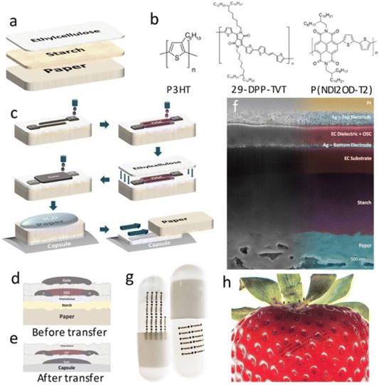 | ||
| Fig. 7 (a) The tattoo-paper stack combines ethylcellulose (EC) with regular paper via a water-soluble starch/dextrin layer, with a non-proportional layer-thickness representation; (b) molecular structures of the semiconductor materials used in the study are depicted; (c) a detailed procedure for creating OFETs on tattoo paper is provided; (d and e) the diagrams illustrate the device structure before (d) and after (e) the transfer process; (f) the SEM image reveals the cross-section of the tattoo-paper device; (g and h) the photos demonstrate silver electrodes transferred onto a pharmaceutical capsule (g) and a strawberry (h), highlighting the practical use of this technology for incorporating electronic components into diverse items, including pharmaceuticals and food products. Reproduced from ref. 44 with permission of Wiley. | ||
Caironi and his research group delved into the utilization of chitosan to print a chitosan-gated transistor (Fig. 8), an easily accessible and cost-effective edible polysaccharide with nutritional value. These transistors featured gold source and drain electrodes printed through inkjet technology, along with a cost-efficient inkjet-printed silver top gate.45
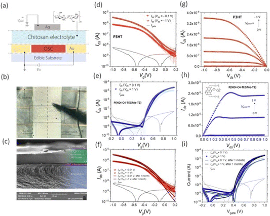 | ||
| Fig. 8 (a) Scheme of the device structure, with the structure of chitosan; (b) photos of chitosan-gated transistor; (c) SEM cross-section of chitosan-gated transistor; (d) transfer characteristic curves for the p-type chitosan-gated transistor; (e) output characteristic curves for the p-type chitosan-gated transistor; (f) transfer characteristic curves for the n-type chitosan-gated transistor; (g) output characteristic curves displaying the linear and saturation regimes for the n-type chitosan-gated transistor; (h) long-term stability of fully printed p-type chitosan-gated transistors over a month; (i) long-term stability of fully printed n-type chitosan-gated transistors over a month. Reproduced from ref. 45 with permission of the Royal Society of Chemistry. | ||
In the absence of approved edible semiconductor materials, the team demonstrated that chitosan-gated transistors can adapt to both hole- and electron-transporting materials using biocompatible polymers.
In recent decades, there has been a growing fascination with melanin and melanin-like materials as pliable, biocompatible functional substances for integration into bioelectronic and optoelectronic devices. Their unique water-dependent conductivity and exceptional biocompatibility have propelled their use. Nevertheless, during the initial stages of their development, challenges such as limited solubility and relatively modest electronic conductivity hindered their progress within these technological domains.46
In flexible organic bioelectronics, a promising frontier lies in the fusion of OFETs and OECTs with textiles, giving rise to electronic textiles or e-textiles. The evolution of flexible electronics represents a significant leap in technology, enabling the creation of advanced products that maintain their functionality, even under continuous deformation. This ground-breaking progress has captured the attention of both academic researchers and industry, particularly in the last decade.9,47
OFETs come with several distinct advantages when applied in wearable technology and e-textiles, making them a compelling choice for integration. These advantages include: (i) low-temperature solution processability: OFETs can be manufactured using low-temperature solution-based methods, making them compatible with a wide range of substrates, including plastics and biodegradable materials; (ii) mechanical flexibility: the organic materials inherent to OFETs exhibit natural flexibility, aligning seamlessly with the requirements of flexible and lightweight product designs.48
These unique features position OFETs as an attractive option for developing innovative, bendable, and lightweight electronic devices that seamlessly blend into various applications, such as wearable health-monitoring systems, flexible displays, and smart textiles. Importantly, OFETs can be configured in two essential forms to address specific electrical and mechanical challenges: planar OFETs (POFETs) and vertical OFETs (VOFETs).
POFETs typically have a layered structure with a thin organic semiconductor (OS) film between two metallic electrodes, the source, and drain. A third electrode, the gate, is separated from the OS layer by an insulator. Unlike traditional metal-oxide semiconductor field-effect transistors (MOSFETs), POFETs rely on the accumulation of charge carriers at the interface between the insulator and the semiconductor for channel formation, making them voltage-controlled current sources.48
On the other hand, VOFETs have a unique vertical stack design with a diode cell above a capacitor unit. The lower electrode serves as the gate, the intermediate electrode functions as the shared source, and the upper electrode operates as the drain. This innovative setup overcomes challenges related to charge transport initiation within the organic semiconductor layer. By using an extremely thin source electrode layer and a supercapacitor, high electric fields are generated at the interface between the source electrode and the OS layer. Alternatively, modifying the spatial structure of the source electrode, such as creating perforations, mitigates the electrode screening effect and improves VOFET performance.48
To enable effective communication between organic semiconductors and biological systems, careful adjustment of material properties is crucial. This tuning should promote cell adhesion and support cell proliferation and growth, and has significant potential in regenerative medicine and tissue engineering.49,50
Conjugated polymers, particularly donor–acceptor conjugated molecules, offer a promising strategy for achieving customizable surface properties to manipulate cell adhesion and cellular behaviour. While these polymers have been mainly used in devices like OECTs, their potential as biomaterials for regenerative medicine remains largely unexplored.
Previous research has primarily focused on conductive polymers offering both electrical stimulation capabilities and controlled surface properties beneficial for cell regeneration. Additionally, conductive polymers like polypyrrole (PPy) and poly(3,4-ethylenedioxythiophene):polystyrenesulfonate (PEDOT:PSS) undergo doping during synthesis, which can be regulated to finely adjust surface properties, creating new opportunities at the intersection of materials science and biology. In one study by Schroeder and colleagues, thin films of poly(diketopyrrolopyrrole terthiophene) (DPP3T) were doped using different dopants to influence cell adhesion and cell viability. The use of p-type dopants was explored to modify surface properties and charge, thus affecting cellular interactions (Fig. 9).51
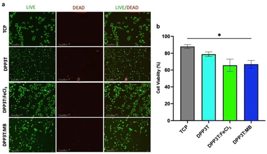 | ||
| Fig. 9 (a) Fluorescence images depicting SCL1.4/F7 Schwann cells that were grown on DPP3T thin films for 48 hours. Live cells are represented in green, thanks to calcein-AM staining, while dead cells are highlighted in red using ethidium homodimer-1 staining; (b) statistical analysis was performed using one-way ANOVA, followed by Tukey’s multiple comparison post-hoc test. Notably, ‘*’ denotes statistically significant differences at the p < 0.05 level. Reproduced from ref. 51 with permission of the Royal Society of Chemistry. | ||
Scientists have examined the impact of doped materials on cell viability after 48 hours of growth on various surfaces (Fig. 10). They compared the doped materials to a pristine DPP3T thin film, with tissue culture plastic (TCP) serving as a positive control. Cell viability was assessed using live and dead cell stains, along with observations of cell morphology.52
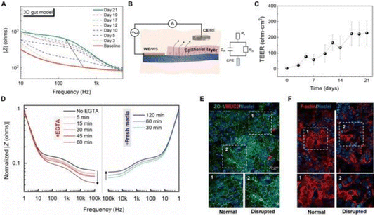 | ||
| Fig. 10 (A) In this representation, time-resolved impedance spectra of a 3D gut epithelial model in the e-transmembrane device allow real-time monitoring of the electrical properties of gut epithelial cells. (B) The electrochemical setup and circuit model, comprising three interconnected elements, are illustrated. (C) The graph displays changes in transepithelial electrical resistance (TEER) of the Caco-2/HT29-MTX cell monolayer over time. (D) Impedance spectrum transformations during disruption with EGTA and subsequent recovery are shown, supported by confocal images (E and F) demonstrating barrier recovery and morphological changes in the intestinal epithelium. Reproduced from ref. 52 with permission of the AAAS. | ||
In recent years, there have been advancements in 3D cell models to overcome the limitations of traditional 2D cell cultures in drug discovery. The “e-transmembrane” is introduced as a novel bioelectronic platform, designed for supporting and monitoring complex 3D cell architectures. It utilizes microengineered scaffolds made of PEDOT:PSS, which serve as both separators for compartmentalized cell cultures and electronic components for real-time monitoring of cell growth and function. This innovative design enables the development of deep, stratified tissues and cell polarization.
Impedance spectroscopy measurements were conducted throughout tissue growth, offering valuable data. The e-transmembrane platform holds significant potential for biologists in high-throughput drug-screening assays.
The researchers comprehensively assessed the e-transmembrane platform’s ability to monitor real-time electrical changes during cell growth. Impedance magnitude and TEER values for epithelial cells were measured over several weeks. Additionally, a calcium switch technique was employed to monitor the effect of EGTA on barrier integrity.
The e-transmembrane platform effectively tracked the recovery process after the removal of EGTA-infused media. The impedance magnitude partially recovered, and the barrier showed distinct regions with expected physiological morphology and others with cell detachment and actin-filament disassembly.
This observed process aligns with the known role of calcium ions in organizing actin filaments in intestinal cells, influencing epithelial junction integrity and maintenance.
3. Emerging organic neuromorphics: challenges and applications
Vertebrates have a complex nervous system that includes the central nervous system (CNS), with the brain and spinal cord, and the peripheral nervous system (PNS), comprising sensory and motor components connected by nerves. These systems work together to control behaviour and movement. Replicating the CNS and PNS functions can advance bioinspired electronics and robotics, creating neuromorphic systems resembling artificial brains and sensory-motor mechanisms. In the human nervous system, there are numerous neurons and synapses that transmit information chemically and electrically. The densely packed cerebral cortex, crucial for cognition, forms the basis for intricate brain operations. Synapses are categorized as chemical or electrical.53Chemical synapses are specialized connections that enable signal transmission between neurons and other cells, vital for intricate neural circuits in the CNS. They play a crucial role in perception, cognitive processes, and the nervous system’s interaction with other bodily systems. Chemical synapses involve the release of neurotransmitters from one neuron into a synaptic cleft, where they bind to receptors on another neuron, ensuring precise signalling.
Electrical synapses are conductive connections occurring in very close proximity between neurons, enabling rapid impulse transmission. Unlike chemical synapses, they do not amplify signals, but they are essential for swift responses, allowing bidirectional impulse transmission.
Researchers are working on replicating biological synapses in neuromorphic electronics to control synaptic functions associated with learning and memory. Organic synapses, with two-terminal (2-T) and three-terminal (3-T) being the main configurations, are fundamental in this field (Fig. 11).54
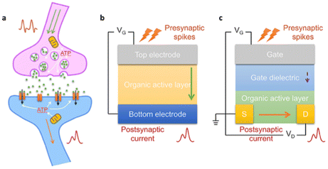 | ||
| Fig. 11 Illustrations of (a) a biological synapse, (b) 2-T organic neuromorphics, and (c) 3-T organic neuromorphics. Reproduced from ref. 54 with permission of Elsevier Ltd. | ||
The 2-T configuration mimics the presynaptic and postsynaptic functions with two distinct electrodes, closely resembling biological synapses but offering simplicity, making them suitable for array construction. Recent advancements in organic memristive devices have brought fast switching, high endurance, and stability, which is valuable for memory technology and neuromorphic computing, especially in pattern recognition tasks.
On the other hand, the 3-T artificial synapse employs three electrodes, each with specific roles. While they offer versatility for various applications, they can complicate wiring, device integration, and scaling. Their advantages include enhanced control and low energy consumption for specific neuromorphic tasks.
Synthetic synapses have benefited from electrolyte-gated organic field-effect transistors (EGOFETs) and OECTs. Nanoparticle organic memory field-effect transistors (NOMFETs) combine computation and memory with nanoparticles functioning as nanoscale capacitors. These devices allow dynamic adjustment of transconductance, vital for neural-network signal transmission. Electrolyte-gated organic synapstors have been proposed for prosthesis applications, mirroring biological synapses’ behaviour, making strides toward efficient neuromorphic systems.55,56
Biocompatibility experiments involved human neuroblastoma stem cells SH-SY5Y and NE-4C cultured on pentacene films integrated into devices. Neurons developed on the device’s surface without significantly affecting its properties, indicating potential applications in prosthesis-related uses, albeit with challenges due to increased semiconductor surface roughness.
Cramer and his research group harnessed EGOFETs to both stimulate and record signals within neural networks originating from murine stem cells.57 These EGOFETs had an ultra-thin 9 nm semiconductor layer and an integrated polystyrene pool for cell culture. Remarkably, these devices proved to be robust in aqueous environments without requiring additional protective layers. They successfully induced the neuronal differentiation of murine neural NE-4C stem cells on these EGOFETs, leading to fully functional neuronal networks. These EGOFETs exhibited sensitivity to signals from neurons rather than undifferentiated stem cells, making them valuable for interfacing with neuronal signals, facilitating electrical stimulation, and possibly contributing to stem cell-based therapies, particularly in the context of spinal-cord injuries. Their exceptional stability and sensitivity, based on ultrathin pentacene semiconductor films, make them a promising platform for translating neuronal activity.
Additionally, Lenz and colleagues introduced a ground-breaking vertical architecture for nanoscale EGOTs (electrolyte-gated organic transistors).58 This innovative design ushered in the era of low-voltage neuromorphic computing systems. The vertical architecture significantly reduced the dimensions of EGOTs, allowing seamless integration into various microchips. These EGOTs featured an organic semiconductor layer of only 2 nm thickness, composed of a diketopyrrolopyrrole–terthiophene donor–acceptor polymer (DPP3T), coupled with an electrolyte, 1-ethyl-3-methylimidazolium bis(trifluoromethylsulfonyl)imide ([EMIM][TFSI]). Remarkably, these EGOTs exhibited artificial synaptic behaviour, including both short- and long-term plasticity. They could induce postsynaptic spikes via application of electrical pulses to the gate electrode, highlighting the potential of EGOTs as artificial synapses. The devices demonstrated remarkable stability, with minimal shifts in threshold voltage and on-current, even after three months of storage. They consistently operated for a minimum of 50 minutes without significant degradation, solidifying their potential as a platform for transducing neuronal activity in neuromorphic computing systems.
This innovative operational principle of artificial synapses has significant potential, not only for computing systems but also for bioelectronic applications. In scenarios where interfacing with neuronal cells is crucial, such as in biosensors, it is essential for devices to operate efficiently at low voltage levels to accurately capture and transduce bioelectric signals from cells and tissues. This aspect of low-voltage operation is vital for successfully integrating these artificial synapses into bioelectronic systems.8,59,60
Early demonstrations of neuromorphic capabilities in OECTs have been reported. For instance, eight OECT devices have been integrated into an adaptive network based on polyaniline fibres, laying a strong foundation for organic-based neuromorphic circuits known for their adaptability and dynamic responsiveness.61
Malliaras and his research group explored the potential of OECT devices for neuromorphic applications. They used as the channel material and investigated how the duration of polarization pulses affected the device responses. Their findings represented a significant step forward in the development of organic-based neuromorphic circuits, particularly for processing spatiotemporal information.62
Salleo and his team enhanced OECT devices for neuromorphic purposes by incorporating a polyethyleneimine (PEI)-blended PEDOT:PSS channel layer to control channel conductivity.63 These devices exhibited a remarkable density of non-volatile states, providing a wide range of conductance levels for computational tasks. By adjusting the parameters of presynaptic pulses, they achieved paired-pulse facilitation (PPF) at short intervals, closely resembling the behaviour of biological synapses. These devices showed great promise in terms of energy efficiency, operational speed, and overall performance, enabling the simulation of a neural network with high accuracy in image classification tasks.
Pecqueur et al. developed an OECT optimized for computing applications, utilizing a spatial reservoir strategy. They created artificial synapses through the electropolymerization of 2-(2-thienyl)-(3,4-ethylenedioxythiophene) (TEDOT) on an array of electrodes.64,65 These OECT devices operated in p-type accumulation mode, requiring lower gate voltages for switching compared to depression-mode devices like PEDOT:PSS. The synaptic properties were thoroughly analysed, emphasizing their variability, and the devices found practical use in reservoir computing, achieving real-time classification of pulse-frequency modulated signals with remarkably low error rates. The study highlighted the significance of materials with inherent variability in the field of neuromorphic applications.
Paulsen et al. integrated OECT devices with a photoresistor and a pressure sensor, allowing them to correlate light and pressure inputs for associative learning.29 They used innovative materials to enhance hysteresis in output curves and observed improved neuromorphic properties, including paired-pulse facilitation (PPF) and paired-pulse potentiation (PTP). The synaptic circuit they designed successfully associated light and pressure as conditioned and unconditioned stimuli, demonstrating associative learning. This study emphasized the value of combining volatile and non-volatile components in neuromorphic circuits, opening possibilities for advanced computing applications.
In their study, Nguyen-Dang et al. introduced a novel gelatine–glycerol gel designed for use as a solid electrolyte in OECTs (Fig. 12).66 This achievement not only brought forth a new biomaterial option for OECTs but also set the stage for future explorations in biomaterial-based electronics. The scientists conducted a comprehensive examination of the gelatine–glycerol gel, particularly focusing on its adjustable ionic conductivity. This thorough analysis was instrumental in understanding the gel’s characteristics and its applicability in electronic contexts. The study effectively demonstrated the application of a gelatine–glycerol gel as a solid-state electrolyte in OECTs. They introduced novel device configurations, achieving remarkable performance metrics, and shed light on the underlying mechanisms of these biogel-based OECTs. Furthermore, the research highlighted the potential of these devices to mimic synaptic behaviours and function as artificial synapses, including frequency-based short-term plasticity. This adaptability opens doors to applications where these devices can emulate and reproduce synaptic functions, significantly impacting the field of neuromorphic computing and related areas. Moreover, in the case of a dehydrated biogel OECT with 50% glycerol content, it exhibited favourable state retention and programmable redox memory, rendering it suitable for specific use cases. Furthermore, a hydrated biogel OECT operating under high humidity displayed behaviours akin to those of liquid-electrolyte OECTs, encompassing pair-pulse depression, emphasizing its versatility and applicability under various environmental conditions.
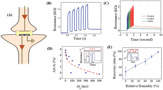 | ||
| Fig. 12 (A) Neuromorphic features of a biogel-modified OECT. (B–D) Resistance measurements over time and with pulses, and (E) evaluation of recovery performance correlated with relative humidity. Reproduced from ref. 66 with permission of Wiley. | ||
Under low-humidity conditions, biogel OECTs demonstrated a remarkable ability to retain the doping state of PEDOT:PSS, despite having less-than-optimal electrolyte conductivity. This intriguing behaviour suggests that the retention of the doping state in biogel OECTs might be linked to the rate of electrochemical doping and de-doping reactions, which varies with humidity levels. The study primarily investigated the short-term synaptic functions of these OECTs, which are crucial for their application as artificial synapses. However, there is a recognized need to explore these devices further, especially in terms of their ability to maintain their functionality over extended periods, thereby achieving long-term plasticity.
In a separate development, researchers led by Sarkar introduced an innovative organic artificial spiking neuron (OAN) that operates within a liquid environment.67 This unique neuron is highly sensitive to ionic species typically found in the extracellular space. The neuron effectively mimics the behaviour of biological neurons, responding to changes in ionic concentrations and displaying spiking responses that are comparable to those seen under physiological and pathological conditions. Furthermore, the OAN can modulate its excitability and generate spikes in response to alterations in ionic concentrations and biomolecules. It even exhibits ion-specific oscillations, emulating the dynamics of ion channels. The ability of the OAN to interface with biological membranes and react in real-time opens a realm of possibilities in the fields of bio-interfacing and neuromorphic computing.
Meanwhile, the emerging field of sensorimotor nervetronics is making strides toward replicating human sensory and motor systems using organic components. Krauhausen et al. introduced an innovative organic neuromorphic circuit capable of facilitating sensorimotor integration.68 This circuit enabled an autonomous robot to learn and navigate a two-dimensional maze by interacting with its sensorimotor system in real-time. The association between sensory inputs and motor actions within this organic neuromorphic circuit proved to be essential for the robot’s successful navigation. Importantly, the robot operated independently and was powered by batteries, demonstrating the significant potential of organic neuromorphic electronics for energy-efficient mobile applications.
Overall, these developments highlight the progress in organic electronics and neuromorphic computing, offering promising avenues for future research and applications in various fields, including biointerfacing, robotics, and advanced computing. The study demonstrated the feasibility of employing organic neuromorphic circuits for tasks requiring adaptive and context-dependent behaviours, representing a significant advancement in the fields of robotics and artificial intelligence.
Additionally, Shim and colleagues introduced a fully elastic synaptic transistor constructed entirely from organic materials (Fig. 13).69 This innovation was accompanied by the development of a neurologically integrated electronic skin, presented in a fully flexible and elastic format. The core components included an elastic semiconductor, an elastic conductor, and an elastic gate dielectric. This electronic skin was capable of real-time interaction with a robotic hand, enabling tactile communication and control and demonstrating its potential for advanced human–robot interaction applications.
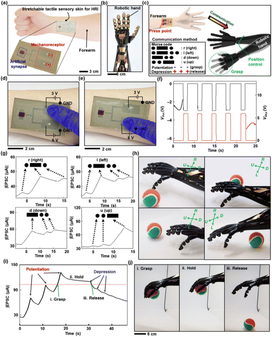 | ||
| Fig. 13 (a–c) A flexible neural electronic dermis has been developed for Human–Robot Interactions (HRIs). This technology is applied to the forearm and allows for tactile communication and control between a human and a robotic hand. (d–f) It operates by converting tactile signals into Morse code using an adaptable neural electronic dermis with mechanoreceptors. (g–j) The system enables real-time interaction, allowing the robotic hand to perform various tasks based on decoded signals from the electronic skin. This advancement holds significant potential for HRIs and demonstrates the feasibility of using organic neuromorphic circuits in robotics and artificial intelligence. Reproduced from ref. 69 with permission of Springer Nature. | ||
While previous research efforts have mainly focused on emulating chemical synapses, there is growing interest in electrical synapses, which are expected to enhance the functionalities and efficiency of neuromorphic electronics in the near future.10,60
4. Bioelectronics for biosensing applications
Transitioning to biosensing applications necessitates the incorporation of liquid electrolytes, resulting in substantial capacitances within the range of 1 to 10 μF cm−2.47 These capacitances significantly surpass those of traditional ‘high-k’ dielectric materials like Ta2O5, often by a factor of approximately ten, especially when considering a 100 nm thick film. Higher capacitances are directly correlated with lower voltages (typically <2 V). This can be better understood from the key equation (eqn (1)) of drain current for a transistor operating in the linear regime (VD ≪ VG): | (1) |
The formula uses the symbols W for channel width, L for channel length, μ for carrier mobility, and VG, VD, and VT for gate, drain, and threshold voltages, respectively. Electrolyte-gating provides various advantages, including reducing source and drain contact resistances, enabling innovative device structures, allowing the use of printable solid electrolytes, and facilitating the integration of electrolyte-gating into biosensors.
In the quest for more precise diagnostics, especially in distinguishing lowgrade from high-grade mucinous cystic lesions in pancreatic cancer, researchers have focused on investigating potential markers, possibly at the level of single molecule.21,22 The markers KRAS and MUC1, which are specific to mucinous lesions, have been effectively tested on a platform named “SiMoT” in both phosphate buffered saline (PBS) and whole human blood serum. These findings offer promising prospects for enhancing diagnostic accuracy, and are discussed in more detail in the following paragraphs.23,70
In the context of the European project “SiMBiT”, Torsi and colleagues introduced a ground-breaking single-molecule transistor (SiMoT). This device achieved the world record for detection limits in label-free assays by immobilizing approximately 1012 anti-human-Immunoglobulin-G (anti-IgG)-capturing antibodies on a millimeter-sized gate electrode. The SiMoT system, featuring a dual-gate structure, was developed using innovative, scalable, and large-area-compatible methods. Researchers successfully employed the SiMoT platform for the analysis of KRAS and MUC1 mucinous lesions in blood serum samples, achieving single-molecule detection sensitivity.23–25
Fig. 14a schematically illustrates the SiMoT device, which includes a lateral gate for reference (Fig. 14b), a sensing gate (Fig. 14c), and a printed poly(3-hexylthiophene) layer inkjet-printed between interdigitated electrodes to form the channel between the source and drain electrodes. The sensing gate electrode was modified using a mixed self-assembled monolayer (SAM) to immobilize receptors for MUC1 and KRAS (Fig. 14d) detection at the single-molecule level, as depicted in the graph in Fig. 14e.
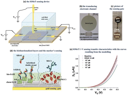 | ||
| Fig. 14 (a) Schematic of the SiMoT device; (b) the lateral gate; (c) the sensing gate; (d) immobilization procedures for anti-MUC1 and b-KRAS; and (e) transfer curves for the detection of KRAS at the single-molecule level. Reproduced from ref. 24 with permission of Wiley. | ||
Additionally, both EGOFETs and OECTs have been utilized for cytokine detection. Casalini and colleagues proposed two distinct approaches for immobilizing anti-IL4 to enable the specific detection of IL-4: covalent attachment and noncovalent attachment.71 The latter, involving noncovalent interaction with protein G, proved to be more effective for cytokine detection due to a higher likelihood of specific binding events.
In this context, SAMs have been primarily employed for functionalizing gate electrodes, initially used to control contact resistances. SAMs have become widely adopted in organic electronics for manipulating the interfacial properties of devices, enhancing stability, responsiveness, and enabling innovative experiments. SAM-functionalized organic devices have successfully bridged the gap between molecular and organic electronics.
Moreover, field-effect transistor (FET)-based sensors rely on electrostatic gating of thin-film semiconductor channels through target–receptor interactions for signal transduction and amplification. Overcoming the fundamental challenges of shielding in ionic solutions and the impact of small target molecules is crucial for improving the sensitivity and effectiveness of receptor-modified FETs in target-molecule detection.72
Andrews and her team pioneered aptamer-modified FETs for electronic detection of small molecules. They covalently modified thin-film In2O3 FETs with aptamers specific for dopamine and serotonin, showcasing remarkable responsiveness even in physiological fluid environments with extremely short Debye screening lengths. These aptamer-based FETs demonstrated high selectivity for their respective targets, making them valuable for sensitive and specific detection.
Weiss and collaborators have introduced a novel approach for detecting oligonucleotide sequences and single nucleotide variations (SNVs) using ultrathin-film quasi-2D metal oxide FETs, as shown in Fig. 15.73 This method offers an innovative pathway for molecular sensing and genomics research due to its potential for highly sensitive and specific genetic information detection. In their study, they modified the semiconductor channel material of FETs with single-stranded DNA (ssDNA) to enable the detection of complementary DNA hybridization.
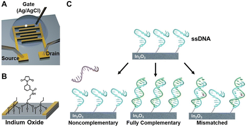 | ||
| Fig. 15 (A) These transistors, measuring 2 × 3 mm2, utilized a 4 nm In2O3 channel and featured interlocked electrodes made of a 10 nm Ti adhesion layer and a 30 nm top Au layer. The transistors operated using a solution-gated system with a reference gate electrode composed of Ag/AgCl. (B) Additionally, the text discusses the functionalization of these transistors with thiolated single-stranded DNA (ssDNA) through a complex process involving silane compounds and linkers. (C) Subsequently, the transistors were exposed to various DNA sequences, including noncomplementary, fully complementary, or mismatched ones. Reproduced from ref. 73 with permission of the American Chemical Society. | ||
FET arrays were fabricated using an ultrathin In2O3 layer (about 4 nm thick) as the channel material through a high-throughput solution-processable sol–gel method. ssDNA probes, in the form of thiolated probes, were functionalized onto the FET surfaces. These probes were attached through self-assembled silanes on the indium oxide channels, employing an amine–thiol linker.
Subsequently, individual FETs equipped with ssDNA probes were exposed to solutions containing different oligonucleotide targets. This included noncomplementary targets, fully complementary targets, or targets with single base-pair mismatches compared to the probes on the FET surfaces. Notably, the FETs could distinguish between responses associated with single base-pair mismatches of various types and positions, demonstrating potential for SNV genotyping, enabling the identification of even minor genetic differences.
Furthermore, within the realm of biosensor technologies, one persistent challenge is nonspecific binding. This is primarily due to an incomplete understanding of this phenomenon, which continues to be a subject of scientific discussion. Given these challenges, introducing theoretical models to predict biosensor behaviour under physiologically relevant conditions is vital. These models serve as a foundation for optimizing sensor performance and estimating theoretical detection limits.74
Additionally, in biosensing applications related to bioelectronics, OECTs have been utilized in biocatalytic biosensors, particularly for detection of metabolites like glucose and lactate. For instance, Inal et al. created an electronic metabolite sensor by physically adsorbing the enzyme on the surface of an organic semiconductor using an n-type copolymer. This device effectively detected glucose levels in saliva, demonstrating impressive sensitivity and selectivity, and a broad detection range.75
Notably, the performance of this glucose sensor relied on the O2 sensitivity of the n-type film, where glucose binding to the enzyme caused changes in the film’s conductivity. To enhance glucose sensitivity, Ohayon et al. employed multiphoton lithography to 3D-print oxygen-sensitive materials encapsulating glucose oxidase (GOx).76
In the study of OECTs, Torricelli and colleagues conducted a comprehensive investigation into the ionic–electronic interactions within these devices. They revealed that the measurements were comprehensively explained by the electrostatic bulk uptake of ions within the OECTs, which neutralized both fixed and mobile electronic charges. This understanding led to the development of OECT unipolar inverters exhibiting remarkable characteristics in electronics.77
Moreover, OMIECs have been used for sensing platforms. van de Burgt and collaborators introduced a flexible circuit that processes signals like electromyograms (EMGs) and electrocardiograms (ECGs) in a neuromorphic classification array. The system utilizes a single polymer mixed conductor to amplify signals and function as a neuromorphic memory element, allowing fine-tuning of gain properties through conductance modulation. This non-volatile adjustment enhances the potential for hardware neural network integration and real-time signal classification.59
Additionally, the utilization of organic thermoelectric materials has been explored for self-powered wearable biosensors. Organic thermoelectrics (OTEs) have gained attention due to their favourable characteristics, such as low toxicity, abundance of constituent elements, and ease of processing. However, OTE-based self-powered sensors are still an emerging concept with limited research and reports to date.
To demonstrate the practical applicability of these materials in the field of wearable sensors, an 8-couple thermoelectric (TE) “bracelet” device was utilized to provide power to a single NL (Nax(Ni-ett)n and PEDOT:PSS) stripe sensor (Fig. 16).78 This setup results in noticeable fluctuations in current and voltage signals as the finger moves, illustrating the potential of these materials for self-powered sensors.
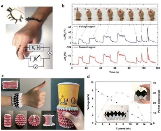 | ||
| Fig. 16 (a) A self-powered thermoelectric (TE) device in the form of a “bracelet”. The device incorporates 8 TE couples and is designed to generate power to operate a strain-sensing component that functions as a motion detector for the index finger. (b) It demonstrates responsiveness to different finger positions by utilizing a temperature difference of about 20 °C. (c) The concept of TE devices with multiple couples is introduced, taking inspiration from the origami “magic ball” design. (d) Power output of a 6-couple TE device when subjected to a 20 °C temperature difference. Reproduced from ref. 78 with permission of Wiley. | ||
Additionally, more complex device designs were explored, inspired by origami principles that transform 2D materials into 3D shapes. These structures consist of p–n TE legs connected in series or parallel to enhance power output and reliability. For instance, a basic 6-couple TE device achieved a power output of 30 picowatts when exposed to a 20 °C temperature difference. These applications open possibilities for use in inflatable and 3D-conformable surfaces, including in soft robotics, intelligent packaging, wearables, automotive applications, and the Internet of Things.
5. Wearable bioelectronics for continuous biomarker monitoring
Detecting chemicals in body fluids, gaseous pollutants or physical inputs without invasive and costly analytical tools is a promising solution for future healthcare needs.79,80 Traditional silicon-based electronic devices have limitations in biological systems due to their reliance on electrons as charge carriers, while organic materials offer versatile solutions. Conducting and semiconducting organic materials bridge biology and electronics by allowing electronic and ionic conduction. They can be tailored with specific receptors for highly sensitive and selective chemical detection, making organic bioelectronics valuable for healthcare applications.81,82Stretchable electronic devices for wearables rely on the flexibility of thin-film transistors. Achieving stretchable semiconductors involves introducing materials that accommodate strain while preserving charge transport properties. Conjugated polymers with modified sidechains and segmented backbones exhibit stretchability by facilitating non-covalent crosslinking. These materials maintain high field-effect mobility performance even after undergoing strain and recovery cycles, making them suitable for wearable devices. Researchers explored also stretchable devices' field-effect mobility under various mechanical strains and movement conditions, demonstrating their durability. Additionally, the polymer semiconductor exhibits healing capability using solvent and thermal treatments.
An innovative interface, called BIND (biphasic, nano-dispersed), enables the connection of soft, rigid, and encapsulation modules in stretchable devices (Fig. 17).83 This interface, composed of polymer and metal nanostructures, facilitates module assembly without the need for pastes. Modules connected with BIND show remarkable mechanical and electrical stretchability. The BIND interface streamlines the development of stretchable devices for on-skin and implantable applications, as demonstrated in in vivo neuromodulation and on-skin electromyography devices. This plug-and-play interface simplifies device construction and offers superior performance compared to conventional paste connections.
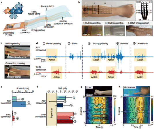 | ||
| Fig. 17 (a) Illustration depicting the EMG electrode array structure. (b) Photograph showcasing the EMG electrode array placement on a human arm. (c) Images displaying a BIND connection before and after applying pressure with a tweezer clamp. (d) Average EMG signals obtained from 21 channels, recorded during experiments involving pressing and releasing, with (e) a comparison between the BIND electrode and the control electrode regarding artifacts. (f) Evaluation of the BIND electrode’s signal-to-noise ratio. (g and h) Photographs and intensity contour mapping of the 21-channel EMG signals, illustrating actions of fist clenching in the air (g) and stretching fingers underwater (h). Reproduced from ref. 83 with permission of SpringerNature. | ||
On-skin EMG electrodes often face mechanical challenges like pressure and strain at their connection points. These stresses can lead to noisy signals and electrode malfunction. The BIND electrode overcomes these challenges, staying resilient when pressure is applied using a tweezer clamp, resulting in clear signals. In contrast, the control ACF-connected electrode shows weakened and noisy signals under pressure. The BIND electrode has smaller artifacts during pressing (0.03 vs. 0.24 mV) and releasing (0.12 vs. 0.80 mV). It maintains a high signal-to-noise ratio (SNR) during various hand and finger movements, both during and after pressing. In contrast, the control electrode experiences significant signal loss and incomplete recovery. The BIND electrode can withstand strains up to 50%, exhibiting fewer artifacts and a higher SNR during stretching. It effectively maps EMG signals for various gestures and performs well underwater and on sweaty skin after exercise.
Monitoring mechanical forces on tendons post-surgery for personalized rehabilitation has been challenging. Bao et al. introduced an implantable biodegradable sensor capable of independently measuring strain and pressure. It can detect tiny strains (0.4%) and low pressures (equivalent to a grain of salt). The sensor has minimal hysteresis, millisecond-level response time, and remarkable cycling stability. An in vivo study in a rat model showed excellent biocompatibility and functionality, highlighting its potential for real-time tendon-healing monitoring.84
Mechanical failure of π-conjugated polymer thin films under cyclic loading is a common issue. Gu et al. introduced a semiconducting composite with butyl rubber (BR) as the elastomer matrix to resist crack propagation, exhibit self-healing properties, and enhance ambient stability.85
The next generation of wearable electronics requires mechanical flexibility and stretchability. Photodetectors based on organic polymers and molecules offer these characteristics, along with excellent light-sensing performance and biocompatibility, making them promising alternatives to rigid inorganic photodetectors.86
6. Conclusions and outlooks
Bioelectronics are currently used in a huge variety of applications, considering the ongoing revolution in personalised medicine and the ‘Green Revolution’, as well as energy management. In all these applications, bioelectronic devices are usually exposed to high-salt aqueous solutions, which can be corrosive to traditional electronic materials. Some applications only need short-term operation (like cutaneous monitoring), while others require long-term in vivo use (such as implantable stimulators). Ensuring the stability of organic bioelectronic materials is crucial for both device performance and their interaction with complex biological systems (considering sensing and neuromorphic applications). To enhance the morphological stability of organic materials, approaches like post-deposition cross-linking or introducing non-covalent intermolecular interactions can be employed.Bioelectronics is poised to make a significant impact on disease diagnosis and treatment. Biosensors capable of detecting biomarkers in blood or other bodily fluids at the single-molecule level can identify diseases, including cancer, at early stages before symptoms manifest. This early detection allows for timely intervention and treatment, ultimately improving patient outcomes and reducing healthcare costs. Bioelectronics also has the potential to develop less invasive and more effective therapies, especially considering the advancements in organic neuromorphics.
In addition, the proliferation of wearable bioelectronic devices, such as fitness monitors and smartwatches, is already evident. These devices are becoming increasingly sophisticated, monitoring vital signs and health metrics in real time. This trend could enable remote patient monitoring, facilitating healthcare providers in remotely tracking patients’ health and intervening when necessary. Implantable bioelectronics devices like pacemakers and cochlear implants have significantly enhanced the lives of millions. These devices are expected to advance further, potentially incorporating features like drug delivery or real-time monitoring of physiological parameters, expanding their utility.
Bioelectronics is set to play a pivotal role in the advancement of biotechnology and biomedicine. By offering new tools for studying biological systems, bioelectronics can accelerate discoveries in these fields. Biosensors capable of detecting specific molecules could aid in the study of cellular signalling pathways, while implantable devices may monitor brain neuron activity.
Ultimately, bioelectronics is anticipated to play a critical role in the development of precision medicine. It can allow personalization of treatments based on an individual’s genetic makeup and medical history. For example, biosensors detecting genetic mutations can identify patients likely to respond to specific therapies, while implantable devices can deliver personalized medication and therapies.
The potential applications of bioelectronics are vast, holding great promise for the advancement of healthcare and biomedicine. As the field continues to evolve, it is likely that new innovations and applications will emerge, further expanding the influence of bioelectronics in these vital areas.
Author contributions
All authors contributed to writing and revising the manuscript. The final version has been approved by all authors. L. T. is responsible for funding acquisition.Conflicts of interest
There are no conflicts to declare.Acknowledgements
The following funding agencies are acknowledged: Biosensori analitici usa-e getta a base di transistori organici auto-alimentati per la rivelazione di biomarcatori proteomici alla singola molecola per la diagnostica decentrata dell’HIV (6CDD3786); Research for Innovation REFIN—Regione Puglia POR PUGLIA FESR-FSE 2014/2020; Dottorati innovativi con caratterizzazione industrial—PON R&I 2014–2020; “Sensore bio-elettronico usa-e-getta per l’HIV autoalimentato da una cella a combustibile biologica” (BioElSens&Fuel); SiMBiT—Single molecule bio-electronic smart system array for clinical testing (grant agreement ID: 824946); PMGB—Sviluppo di piattaforme meccatroniche, genomiche e bioinformatiche per l’oncologia di precisione—ARS01_01195-PON “Ricerca e Innovazione” 2014–2020; CSGI is acknowledged for partial financial support.Notes and references
- M. Berggren and A. Richter-Dahlfors, Adv. Mater., 2007, 19, 3201–3213 CrossRef CAS.
- J. Rivnay, R. M. Owens and G. G. Malliaras, Chem. Mater., 2014, 26, 679–685 CrossRef CAS.
- G. G. Malliaras, Biochim. Biophys. Acta, Gen. Subj., 2013, 1830, 4286–4287 CrossRef CAS PubMed.
- G. Malliaras and I. McCulloch, Chem. Rev., 2022, 122, 4323–4324 CrossRef CAS PubMed.
- D. Ohayon and S. Inal, Adv. Mater., 2020, 32, 2001439 CrossRef CAS PubMed.
- N. Wang, A. Yang, Y. Fu, Y. Li and F. Yan, Acc. Chem. Res., 2019, 52, 277–287 CrossRef CAS PubMed.
- A. Yasuda and W. Knoll, Organic Bioelectronics for Life Science and Healthcare, Materials Research Forum LLC, 2019 Search PubMed.
- Y. Lee and T. W. Lee, Acc. Chem. Res., 2019, 52, 964–974 CrossRef CAS PubMed.
- Y. Xu, W. Liu, Y. Huang, C. Jin, B. Zhou, J. Sun and J. Yang, Adv. Electron. Mater., 2021, 7, 2100336 CrossRef CAS.
- W. Wang, Y. Jiang, D. Zhong, Z. Zhang, S. Choudhury, J.-C. Lai, H. Gong, S. Niu, X. Yan and Y. Zheng, Science, 2023, 380, 735–742 CrossRef CAS PubMed.
- D. T. Simon, E. O. Gabrielsson, K. Tybrandt and M. Berggren, Chem. Rev., 2016, 116, 13009–13041 CrossRef CAS PubMed.
- A. A. Leonardi, M. J. Lo Faro, C. Di Franco, G. Palazzo, C. D’Andrea, D. Morganti, K. Manoli, P. Musumeci, B. Fazio and M. Lanza, J. Mater. Sci.: Mater. Electron., 2020, 31, 10–17 CrossRef CAS.
- H. Bronstein, C. B. Nielsen, B. C. Schroeder and I. McCulloch, Nat. Rev. Chem, 2020, 4, 66–77 CrossRef CAS PubMed.
- C. Wang, H. Dong, L. Jiang and W. Hu, Chem. Soc. Rev., 2018, 47, 422–500 RSC.
- J. Borges-González, C. J. Kousseff and C. B. Nielsen, J. Mater. Chem. C, 2019, 7, 1111–1130 RSC.
- A. J. Lovinger, D. D. Davis, A. Dodabalapur, H. E. Katz and L. Torsi, Macromolecules, 1996, 29, 4952–4957 CrossRef CAS.
- A. J. Lovinger, D. D. Davis, R. Ruel, L. Torsi, A. Dodabalapur and H. E. Katz, J. Mater. Res., 1995, 10, 2958–2962 CrossRef CAS.
- G. Lanzani, Nat. Mater., 2014, 13, 775–776 CrossRef CAS PubMed.
- C. Müller, L. Ouyang, A. Lund, K. Moth-Poulsen and M. M. Hamedi, Adv. Mater., 2019, 31, 1807286 CrossRef PubMed.
- B. C. Schroeder, T. Kurosawa, T. Fu, Y. C. Chiu, J. Mun, G. J. N. Wang, X. Gu, L. Shaw, J. W. E. Kneller, T. Kreouzis, M. F. Toney and Z. Bao, Adv. Funct. Mater., 2017, 27, 1701973 CrossRef.
- E. Macchia, K. Manoli, B. Holzer, C. Di Franco, M. Ghittorelli, F. Torricelli, D. Alberga, G. F. Mangiatordi, G. Palazzo, G. Scamarcio and L. Torsi, Nat. Commun., 2018, 9, 3223 CrossRef PubMed.
- E. Macchia, F. Torricelli, P. Bollella, L. Sarcina, A. Tricase, C. Di Franco, R. Osterbacka, Z. M. Kovacs-Vajna, G. Scamarcio and L. Torsi, Chem. Rev., 2022, 122, 4636–4699 CrossRef CAS PubMed.
- E. Genco, F. Modena, L. Sarcina, K. Björkström, C. Brunetti, M. Caironi, M. Caputo, V. M. Demartis, C. Di Franco, G. Frusconi, L. Haeberle, P. Larizza, M. T. Mancini, R. Österbacka, W. Reeves, G. Scamarcio, C. Scandurra, M. Wheeler, E. Cantatore, I. Esposito, E. Macchia, F. Torricelli, F. A. Viola and L. Torsi, Adv. Mater., 2023, 35, 2304102 CrossRef CAS PubMed.
- E. Macchia, L. Sarcina, C. Driescher, Z. Gounani, A. Tewari, R. Osterbacka, G. Palazzo, A. Tricase, Z. M. Kovacs Vajna, F. Viola, F. Modena, M. Caironi, F. Torricelli, I. Esposito and L. Torsi, Adv. Electron. Mater., 2021, 7, 2100304 CrossRef CAS.
- E. Macchia, R. A. Picca, K. Manoli, C. Di Franco, D. Blasi, L. Sarcina, N. Ditaranto, N. Cioffi, R. Österbacka, G. Scamarcio, F. Torricelli and L. Torsi, Mater. Horiz., 2020, 7, 999–1013 RSC.
- M. Magliulo, A. Mallardi, R. Gristina, F. Ridi, L. Sabbatini, N. Cioffi, G. Palazzo and L. Torsi, Anal. Chem., 2013, 85, 3849–3857 CrossRef CAS PubMed.
- E. Macchia, K. Manoli, B. Holzer, C. Di Franco, R. A. Picca, N. Cioffi, G. Scamarcio, G. Palazzo and L. Torsi, Anal. Bioanal. Chem., 2019, 411, 4899–4908 CrossRef CAS PubMed.
- E. Macchia, A. Tiwari, K. Manoli, B. Holzer, N. Ditaranto, R. A. Picca, N. Cioffi, C. Di Franco, G. Scamarcio, G. Palazzo and L. Torsi, Chem. Mater., 2019, 31, 6476–6483 CrossRef CAS.
- B. D. Paulsen, K. Tybrandt, E. Stavrinidou and J. Rivnay, Nat. Mater., 2020, 19, 13–26 CrossRef CAS PubMed.
- F. Bonafè, F. Decataldo, B. Fraboni and T. Cramer, Adv. Electron. Mater., 2021, 7, 2100086 CrossRef.
- X. Wu, T. L. D. Tam, S. Chen, T. Salim, X. Zhao, Z. Zhou, M. Lin, J. Xu, Y. L. Loo and W. L. Leong, Adv. Mater., 2022, 34, 2206118 CrossRef CAS PubMed.
- S. T. M. Tan, A. Gumyusenge, T. J. Quill, G. S. LeCroy, G. E. Bonacchini, I. Denti and A. Salleo, Adv. Mater., 2022, 34, 2110406 CrossRef CAS PubMed.
- R. Wu, D. Meli and J. Rivnay, Nat. Mater., 2023, 22, 1055–1056 CrossRef CAS PubMed.
- G. Dufil, I. Bernacka-Wojcik, A. Armada-Moreira and E. Stavrinidou, Chem. Rev., 2022, 122, 4847–4883 CrossRef CAS PubMed.
- C. Diacci, T. Abedi, J. W. Lee, E. O. Gabrielsson, M. Berggren, D. T. Simon, T. Niittylä and E. Stavrinidou, iScience, 2021, 24, 101966 CrossRef CAS PubMed.
- A. Armada-Moreira, A. M. Dar, Z. Zhao, C. Cea, J. Gelinas, M. Berggren, A. Costa, D. Khodagholy and E. Stavrinidou, Sci. Adv., 2023, 9, eadh4443 CrossRef CAS PubMed.
- Y. Zhao, S. Gao, J. Zhu, J. Li, H. Xu, K. Xu, H. Cheng and X. Huang, ACS Omega, 2019, 4, 9522–9530 CrossRef CAS PubMed.
- M. Seitanidou, R. Blomgran, G. Pushpamithran, M. Berggren and D. T. Simon, Adv. Healthcare Mater., 2019, 8, 1900813 CrossRef CAS PubMed.
- D. Cherian, A. Roy, A. B. Farinotti, T. Abrahamsson, T. Arbring Sjöström, K. Tybrandt, D. Nilsson, M. Berggren, C. I. Svensson, D. J. Poxson and D. T. Simon, Adv. Healthcare Mater., 2023, 12, 2300550 CrossRef CAS PubMed.
- D. Cherian, A. Armgarth, V. Beni, U. Linderhed, K. Tybrandt, D. Nilsson, D. T. Simon and M. Berggren, Flexible Printed Electron., 2019, 4, 22001 CrossRef CAS.
- D. T. Simon, S. Kurup, K. C. Larsson, R. Hori, K. Tybrandt, M. Goiny, E. W. H. Jager, M. Berggren, B. Canlon and A. Richter-Dahlfors, Nat. Mater., 2009, 8, 742–746 CrossRef CAS PubMed.
- I. Bernacka-Wojcik, M. Huerta, K. Tybrandt, M. Karady, M. Y. Mulla, D. J. Poxson, E. O. Gabrielsson, K. Ljung, D. T. Simon, M. Berggren and E. Stavrinidou, Small, 2019, 15, 1902189 CrossRef CAS PubMed.
- A. S. Sharova, F. Melloni, G. Lanzani, C. J. Bettinger and M. Caironi, Adv. Mater. Technol., 2021, 6, 2000757 CrossRef.
- G. E. Bonacchini, C. Bossio, F. Greco, V. Mattoli, Y. H. Kim, G. Lanzani and M. Caironi, Adv. Mater., 2018, 30, 1706091 CrossRef PubMed.
- A. S. Sharova, F. Modena, A. Luzio, F. Melloni, P. Cataldi, F. Viola, L. Lamanna, N. F. Zorn, M. Sassi, C. Ronchi, J. Zaumseil, L. Beverina, M. R. Antognazza and M. Caironi, Nanoscale, 2023, 15, 10808–10819 RSC.
- J. V. Paulin and C. F. O. Graeff, J. Mater. Chem. C, 2021, 9, 14514–14531 RSC.
- S. H. Kim, K. Hong, W. Xie, K. H. Lee, S. Zhang, T. P. Lodge and C. D. Frisbie, Adv. Mater., 2013, 25, 1822–1846 CrossRef CAS PubMed.
- A. Nawaz, L. Merces, L. M. M. Ferro, P. Sonar and C. C. B. Bufon, Adv. Mater., 2023, 35, 2204804 CrossRef CAS PubMed.
- O. Dadras-Toussi, M. Khorrami, A. S. C. Louis Sam Titus, S. Majd, C. Mohan and M. R. Abidian, Adv. Mater., 2022, 34, 2200512 CrossRef CAS PubMed.
- M. Fahlman, S. Fabiano, V. Gueskine, D. Simon, M. Berggren and X. Crispin, Nat. Rev. Mater., 2019, 4, 627–650 CrossRef CAS.
- R. P. Trueman, P. G. Finn, M. M. Westwood, A. Dey, R. Palgrave, A. Tabor, J. B. Phillips and B. C. Schroeder, J. Mater. Chem. C, 2023, 11, 6943–6950 RSC.
- C. Pitsalidis, D. Van Niekerk, C. M. Moysidou, A. J. Boys, A. Withers, R. Vallet and R. M. Owens, Sci. Adv., 2022, 8, eabo4761 CrossRef CAS PubMed.
- A. E. Pereda, Nat. Rev. Neurosci., 2014, 15, 250–263 CrossRef CAS PubMed.
- Y. Lee, H.-L. Park, Y. Kim and T.-W. Lee, Joule, 2021, 5, 794–810 CrossRef CAS.
- J. Sun, Y. Fu and Q. Wan, J. Phys. D Appl. Phys., 2018, 51, 314004 CrossRef.
- F. Alibart, S. Pleutin, O. Bichler, C. Gamrat, T. Serrano-Gotarredona, B. Linares-Barranco and D. Vuillaume, Adv. Funct. Mater., 2012, 22, 609–616 CrossRef CAS.
- T. Cramer, B. Chelli, M. Murgia, M. Barbalinardo, E. Bystrenova, D. M. de Leeuw and F. Biscarini, Phys. Chem. Chem. Phys., 2013, 15, 3897–3905 RSC.
- J. Lenz, F. Del Giudice, F. R. Geisenhof, F. Winterer and R. T. Weitz, Nat. Nanotechnol., 2019, 14, 579–585 CrossRef CAS PubMed.
- Y. Zhang, E. R. W. van Doremaele, G. Ye, T. Stevens, J. Song, R. C. Chiechi and Y. van de Burgt, Adv. Mater., 2022, 34, 2200393 CrossRef CAS PubMed.
- Y. Van De Burgt, A. Melianas, S. T. Keene, G. Malliaras and A. Salleo, Nat. Electron., 2018, 1, 386–397 CrossRef.
- Y. Tuchman, T. N. Mangoma, P. Gkoupidenis, Y. Van De Burgt, R. A. John, N. Mathews, S. E. Shaheen, R. Daly, G. G. Malliaras and A. Salleo, MRS Bull., 2020, 45, 619–630 CrossRef.
- P. Gkoupidenis, N. Schaefer, B. Garlan and G. G. Malliaras, Adv. Mater., 2015, 27, 7176–7180 CrossRef CAS PubMed.
- S. T. Keene, T. P. A. van der Pol, D. Zakhidov, C. H. L. Weijtens, R. A. J. Janssen, A. Salleo and Y. van de Burgt, Adv. Mater., 2020, 32, 2000270 CrossRef CAS PubMed.
- S. Pecqueur, M. Mastropasqua Talamo, D. Guérin, P. Blanchard, J. Roncali, D. Vuillaume and F. Alibart, Adv. Electron. Mater., 2018, 4, 1800166 CrossRef.
- S. Yamamoto, Polym. Int., 2023, 72, 609–618 CrossRef CAS.
- T. Nguyen-Dang, K. Harrison, A. Lill, A. Dixon, E. Lewis, J. Vollbrecht, T. Hachisu, S. Biswas, Y. Visell and T. Q. Nguyen, Adv. Electron. Mater., 2021, 7, 2100519 CrossRef CAS.
- T. Sarkar, K. Lieberth, A. Pavlou, T. Frank, V. Mailaender, I. McCulloch, P. W. M. Blom, F. Torricelli and P. Gkoupidenis, Nat. Electron., 2022, 5, 774–783 CrossRef.
- I. Krauhausen, D. A. Koutsouras, A. Melianas, S. T. Keene, K. Lieberth, H. Ledanseur, R. Sheelamanthula, A. Giovannitti, F. Torricelli and I. Mcculloch, Sci. Adv., 2021, 7, eabl5068 CrossRef CAS PubMed.
- H. Shim, S. Jang, J. G. Jang, Z. Rao, J. I. Hong, K. Sim and C. Yu, Nano Res., 2022, 15, 758–764 CrossRef CAS.
- D. Blasi, F. Viola, F. Modena, A. Luukkonen, E. MacChia, R. A. Picca, Z. Gounani, A. Tewari, R. Österbacka, M. Caironi, Z. M. Kovacs Vajna, G. Scamarcio, F. Torricelli and L. Torsi, J. Mater. Chem. C, 2020, 8, 15312–15321 RSC.
- S. Casalini, C. A. Bortolotti, F. Leonardi and F. Biscarini, Chem. Soc. Rev., 2017, 46, 40–71 RSC.
- N. Nakatsuka, K. A. Yang, J. M. Abendroth, K. M. Cheung, X. Xu, H. Yang, C. Zhao, B. Zhu, Y. S. Rim, Y. Yang, P. S. Weiss, M. N. Stojanović and A. M. Andrews, Science, 2018, 362, 319–324 CrossRef CAS PubMed.
- K. M. Cheung, J. M. Abendroth, N. Nakatsuka, B. Zhu, Y. Yang, A. M. Andrews and P. S. Weiss, Nano Lett., 2020, 20, 5982–5990 CrossRef CAS PubMed.
- A. Frutiger, A. Tanno, S. Hwu, R. F. Tiefenauer, J. Vörös and N. Nakatsuka, Chem. Rev., 2021, 121, 8095–8160 CrossRef CAS PubMed.
- V. Druet, P. D. Nayak, A. Koklu, D. Ohayon, A. Hama, X. Chen, M. Moser, I. McCulloch and S. Inal, Adv. Electron. Mater., 2022, 8, 2200065 CrossRef CAS.
- D. Ohayon, D. Renn, S. Wustoni, K. Guo, V. Druet, A. Hama, X. Chen, I. P. Maria, S. Singh, S. Griggs, B. C. Schroeder, M. Rueping, I. McCulloch and S. Inal, ACS Appl. Mater. Interfaces, 2023, 15, 9726–9739 CrossRef CAS PubMed.
- P. Romele, M. Ghittorelli, Z. M. Kovács-Vajna and F. Torricelli, Nat. Commun., 2019, 10, 3044 CrossRef PubMed.
- K. Wan, P. J. Taroni, Z. Liu, Y. Liu, Y. Tu, G. Santagiuliana, I. C. Hsia, H. Zhang, O. Fenwick, S. Krause, M. Baxendale, B. C. Schroeder and E. Bilotti, Adv. Electron. Mater., 2019, 5, 1900582 CrossRef CAS.
- P. Bollella, Anal. Chim. Acta, 2022, 1234, 340517 CrossRef CAS PubMed.
- A. Tricase, A. Imbriano, M. Valentino, N. Ditaranto, E. Macchia, C. Di Franco, R. Kidayaveettil, D. Leech, M. Piscitelli and G. Scamarcio, Adv. Sens. Res., 2023, 2300036 CrossRef.
- M. Y. Lee, H. R. Lee, C. H. Park, S. G. Han and J. H. Oh, Acc. Chem. Res., 2018, 51, 2829–2838 CrossRef CAS PubMed.
- J. Y. Oh, S. Rondeau-Gagné, Y. C. Chiu, A. Chortos, F. Lissel, G. J. N. Wang, B. C. Schroeder, T. Kurosawa, J. Lopez, T. Katsumata, J. Xu, C. Zhu, X. Gu, W. G. Bae, Y. Kim, L. Jin, J. W. Chung, J. B. H. Tok and Z. Bao, Nature, 2016, 539, 411–415 CrossRef CAS PubMed.
- Y. Jiang, S. Ji, J. Sun, J. Huang, Y. Li, G. Zou, T. Salim, C. Wang, W. Li, H. Jin, J. Xu, S. Wang, T. Lei, X. Yan, W. Y. X. Peh, S. C. Yen, Z. Liu, M. Yu, H. Zhao, Z. Lu, G. Li, H. Gao, Z. Liu, Z. Bao and X. Chen, Nature, 2023, 614, 456–462 CrossRef CAS PubMed.
- C. M. Boutry, Y. Kaizawa, B. C. Schroeder, A. Chortos, A. Legrand, Z. Wang, J. Chang, P. Fox and Z. Bao, Nat. Electron., 2018, 1, 314–321 CrossRef.
- S. Zhang, Y. H. Cheng, L. Galuska, A. Roy, M. Lorenz, B. Chen, S. Luo, Y. T. Li, C. C. Hung, Z. Qian, P. B. J. St. Onge, G. T. Mason, L. Cowen, D. Zhou, S. I. Nazarenko, R. F. Storey, B. C. Schroeder, S. Rondeau-Gagné, Y. C. Chiu and X. Gu, Adv. Funct. Mater., 2020, 30, 2000663 CrossRef CAS.
- P. C. Y. Chow and T. Someya, Adv. Mater., 2020, 32, 1902045 CrossRef CAS PubMed.
| This journal is © The Royal Society of Chemistry 2024 |

