
 Open Access Article
 This Open Access Article is licensed under a
 Creative Commons Attribution 3.0 Unported Licence
Double-type-I charge-injection heterostructure for quantum-dot light-emitting diodes†
Li-Xi
Wang‡
ab,
Cindy G.
Tang‡
a,
Zhao-Siu
Tan
c,
Hao-Yu
Phua
a,
Jing
Chen
 b,
Wei
Lei
b,
Rui-Qi
Png
*a,
Lay-Lay
Chua
*ac and
Peter K. H.
Ho
a
b,
Wei
Lei
b,
Rui-Qi
Png
*a,
Lay-Lay
Chua
*ac and
Peter K. H.
Ho
a
aDepartment of Physics, National University of Singapore, Lower Kent Ridge Road, S117550, Singapore. E-mail: ruiqi@nus.edu.sg
bJoint International Research Laboratory of Information Display and Visualization, School of Electronic Science and Engineering, Southeast University, Nanjing, People's Republic of China
cDepartment of Chemistry, National University of Singapore, Lower Kent Ridge Road, S117552, Singapore. E-mail: chmcll@nus.edu.sg
First published on 26th May 2022
Abstract
Enforcing balanced electron–hole injection into the emitter layer of quantum-dot light-emitting diodes (QLEDs) remains key to maximizing the quantum efficiency over a wide current density range. This was previously thought not possible for quantum dot (QD) emitters because of their very deep energy bands. Here, we show using Mesolight® blue-emitting CdZnSeS/ZnS QDs as a model that its valence levels are in fact considerably shallower than the corresponding band maximum of the bulk semiconductor, which makes the ideal double-type-I injection/confinement heterostructure accessible using a variety of polymer organic semiconductors as transport and injection layers. We demonstrate flat external quantum efficiency characteristics that indicate near perfect recombination within the QD layer over several decades of current density from the onset of device turn-on of about 10 μA cm−2, for both normal and inverted QLED architectures. We also demonstrate that these organic semiconductors do not chemically degrade the QDs, unlike the usual ZnMgO nanoparticles. However, these more efficient injection heterostructures expose a new vulnerability of the QDs to in device electrochemical degradation. The work here opens a clear path towards next-generation ultra-high-performance, all-solution-processed QLEDs.
New conceptsThis manuscript describes a major breakthrough in the design thinking of charge carrier injection and confinement structures for quantum-dot light-emitting diodes (QLEDs) that can now finally enforce perfect electron–hole recombination efficiency, over an unprecedentedly wide current density and luminance range of 4+ orders of magnitude. Although there are recent reports of very high performance, that performance is strongly peaked over a narrow current density and luminance range, due to the inability of the diode structure to confine electrons and holes over a wide range of operating conditions. Our manuscript reveals the way to fix this, clarifying the general requirement for the double type-I injection heterostructure that has been neglected in the science and technology of QLEDs for the last 30 years. We report here a new approach to device architecture using organic semiconductor layers to implement this double type-I charge-confinement heterostructure through a novel film-transfer method. We discover unity internal quantum efficiency with flat external quantum efficiency characteristics for blue QLEDs, limited only by the radiative efficiency of the emitter. This sets a new benchmark for performance. The approach is also applicable to other novel semiconductors, including perovskites. |
Introduction
A number of breathtaking advances have occurred recently in the development of high-quality core/shell QDs to improve device quantum efficiency (QE) and stability, in particular better surface passivation and stabilization.1–3 QLEDs are now promising candidates for display and lighting applications on account of their inherent solution processability, narrow emission linewidth and wide color gamut. Nevertheless, the device structures are still sub-optimal from the device physics point-of-view.The prevailing QLED charge injection heterostructures are of type-II, with energy offsets at both valence and conduction levels in the same direction, whereas the ideal heterostructure should be type-I, with offsets in the opposite direction. In the ideal double-type-I injection heterostructure (Fig. 1a), holes are injected by a doped hole injection layer (HIL) with the Fermi level aligned close to the valence band (VB) edge of the hole transport layer (HTL), which is further aligned to, or marginally deeper than, the valence level of the QD core in the emitter layer (EML). Correspondingly, electrons are injected by a doped electron injection layer (EIL) with the Fermi level aligned close to the conduction band (CB) edge of the electron transport layer (ETL), which is aligned to, or marginally shallower than, the conduction level of the QD core. This arrangement minimizes energy losses in the carriers before they recombine. Within the EML, carrier tunneling across the QD shell should relieve the need for transport edges of the HTL and ETL to match those of the shell. The ideal injection heterostructure should also present a large unfavorable energy offset to block the exit and thus confine the opposite carriers. The device type-I heterostructure discussed here is different from the internal type-I heterostructure of the core/shell employed to confine the electron and hole wavefunctions to the QD core for efficient radiative recombination.4
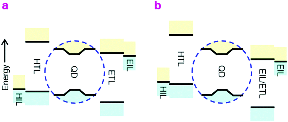 | ||
| Fig. 1 Injection heterostructures. (a) Ideal double-type-I injection/confinement heterostructure QLEDs, and (b) actual double-type-II heterostructure QLEDs in widespread study. The region enclosed by the blue dashed line denotes the core/shell QD, neglecting the wide-gap organic ligand coating which protects the QD but acts as a tunnel spacer to charge carriers. | ||
Due to the deep energy levels of the QD semiconductor and limited availability of charge transport materials, however, the actual devices are usually of the double-type-II heterostructure, especially for blue-emitting QLEDs (Fig. 1b). These devices present considerable thermodynamic barriers to the injection of both carriers into the EML, which causes the diode built-in potential (Vbi) to fall below the emission bandgap. Furthermore, as a consequence of the inevitable asymmetry, electron and hole currents are highly imbalanced at device turn-on. Although the low carrier mobilities within the EML cause carrier density pile-up that advantageously improves the current balance, and hence recombination efficiency, the external QE–current density (η–J) characteristic still tend to exhibit peaking over a relatively narrow current density and luminance range.5,6
This roll-off of QE at high current densities, often called “droop”, has a number of fundamental contributing factors, including electric field quenching,7 Auger recombination,8,9 and Joule heating.10 But an overarching one would be imperfect recombination at both the high and particularly at the low current density range, due to imbalanced injection and/or carrier leakage from the EML. Similar efficiency roll-off also plagues LEDs based on other colloidal nanocrystals, such as perovskites.11,12
Whether type-I injection heterostructures can be fabricated depends on the energy levels of the QD core. The semiconductors making up the core of practical QDs, whether Cd-based II–VI, In-based III–V or (Cu,Zn)(In,Ga)S I–III–VI, generally have very deep VB maximum. For example, CdSe(11![[1 with combining macron]](https://www.rsc.org/images/entities/char_0031_0304.gif) 0) has an ionization energy (IE) of 6.6 eV.13 Curvature, composition grading and, particularly, surface termination effects in their QDs may upshift the energy levels. But the extent of this effect is not fully understood. As a model of high-performance blue-emitting QDs (‘blue-QD’), we choose Mesolight® CdZnSeS/ZnS core/shell QDs. X-ray photoemission spectroscopy suggests that these are gradient-alloyed QDs14 that comprise a small CdZnSeS core and a thick shell of ZnSeS terminating in an outer ZnS layer coated with oleic acid (for XPS, see Fig. S1, ESI†).
0) has an ionization energy (IE) of 6.6 eV.13 Curvature, composition grading and, particularly, surface termination effects in their QDs may upshift the energy levels. But the extent of this effect is not fully understood. As a model of high-performance blue-emitting QDs (‘blue-QD’), we choose Mesolight® CdZnSeS/ZnS core/shell QDs. X-ray photoemission spectroscopy suggests that these are gradient-alloyed QDs14 that comprise a small CdZnSeS core and a thick shell of ZnSeS terminating in an outer ZnS layer coated with oleic acid (for XPS, see Fig. S1, ESI†).
Ultraviolet photoemission spectroscopy (UPS) shows that the VB density-of-states extends well above the −7.5 eV onset expected of bulk ZnS to ca. −6.2 eV (Fig. 2). The emission intensifies with vacuum UV exposure, which evidences its VB origin, since the shell is increasingly exposed by VUV-induced dehydrogenation of the unsaturated organic acid coating.15 The inelastic mean free path of photoelectrons in this energy range for these materials is about 3 Å; therefore, only the shell can be observed. Taking the onset as IE of the QD ZnS shell, we estimate from a rigid shift that the effective valence and conduction levels of the core are −5.7 and −2.9 eV, respectively.16,17 These values are considerably shallower than often assumed for blue-emitting CdSe-based cores, but are in good agreement with systematics of diode behaviour (vide infra). They open the possibility to find polymer organic semiconductors with matching transport levels. For example, poly(9,9-dioctylfluorene-2,7-diyl-1,4-phenylene-N-(m-trifluoromethyl-phenyl)imino-1,4-phenylene) (mTFF), with an effective VB edge at −5.8 eV, could offer a suitable HTL,18 while the usual poly(9,9-dioctylfluorene-2,7-diyl-1,4-phenylene-N-(p-sec-butylphenyl)imino-1,4-phenylene) (TFB), at −5.5 eV, is too shallow. Poly(9,9-bis(4-octylphenyl)fluorene-2,7-diyl) (PFOP) and poly(9,9-dioctylfluorene-2,7-diyl-benzo[2,1,3]-thiadiazole-4,7-diyl) (F8BT), with estimated CB edges at −2.4 and −2.9 eV, respectively, could provide suitable ETLs. The chemical structures of these and other relevant materials are shown in Fig. 3a. The resultant energy-level diagrams, compared to the conventional ‘standard’ one, are shown in Fig. 3b. Although organic ETLs have been suggested before, earlier attempts to use electron transporting materials, such as Alq3 and TPBi, have not been successful, presumably due to poor electron mobility and/or energy mismatch.19
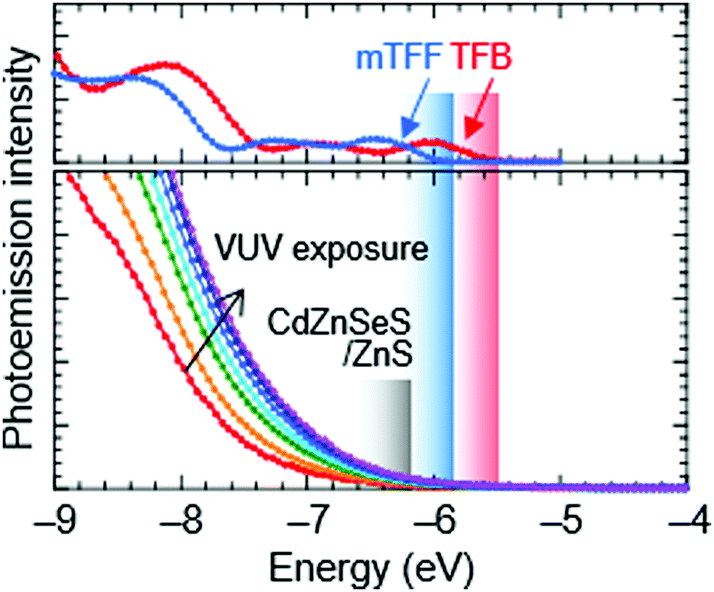 | ||
| Fig. 2 Ultraviolet photoemission spectroscopy of the ionization edge of Mesolight® blue-emitting CdZnSeS/ZnS QDs, and possible hole transporting organic semiconductors. Excitation source, He–I. Energy plotted from the vacuum level. He–I radiation causes dehydrogenation of the unsaturated organic acid coating, which reveals the VB onset at ca. −6.2 eV. The effective VB edges of TFB and mTFF are −5.5 and −5.8 eV, respectively, extrapolated from inflection of the frontier slope. | ||
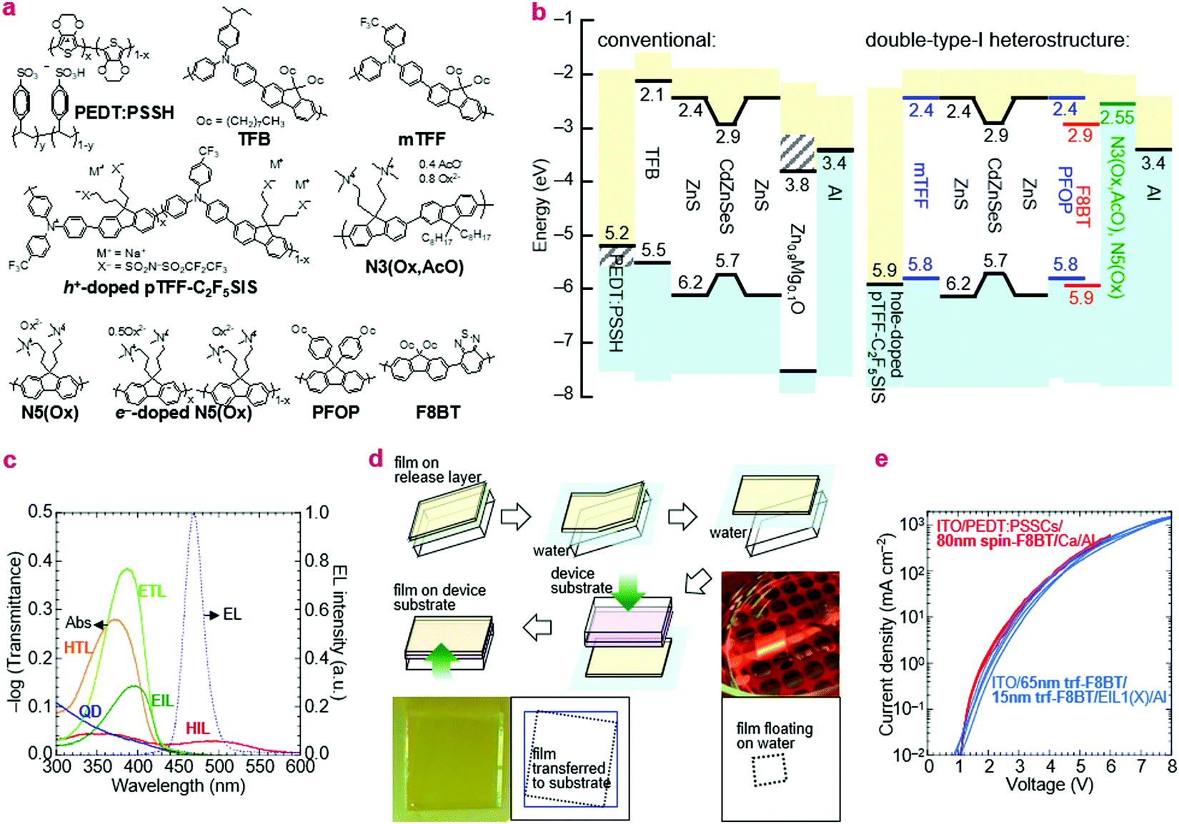 | ||
| Fig. 3 Polymer injection and transport layers. (a) Chemical structure. Doping level is denoted by the value of x in charge per repeat unit: 0 (undoped) ≤ x ≤ 1 (fully doped). (b) Energy-level diagram. Hashed lines indicate uncertainty due to work function shifts. Doped organic semiconductors are depicted as ‘gap-less’ because polaron states exist across the Fermi level. (c) −log(Transmittance) spectra of polymer layers compared to the electroluminescence (EL) spectrum of QDs. (d) Thin-film float-off and pick-up method. The film to be transferred is floated off on water and picked up by the destination device stack. It is visible due to higher reflectance on water and interference contrast on the device stack. (e) Current–voltage characteristics of a spin-on F8BT film and a stack of two transferred films (trf-F8BT) of the same total thickness; two representative diodes are shown for each. | ||
Thus, in this work, we have exploited recently available polymer semiconductors as injection and transport layers to realize the elusive double-type-I injection heterostructures for blue QLEDs. We show that even a rudimentary structure can enforce balanced electron–hole injection and near perfect recombination over an unprecedentedly wide current density range, with near ideal η–J characteristics superior to those of the ‘standard’ structure based on TFB as the HTL20 and ZnMgO as the EIL.21–23 We also show that the polymer layers do not degrade the QDs, unlike ZnMgO. Thus, organic semiconductors possess not only sufficient latitude for energy-level engineering but also chemical compatibility and suitable carrier mobilities to manage injection and recombination in QLEDs.
Results and discussion
Material selection
For the EML, we used two-monolayer-thick (20 nm) Mesolight® blue-QDs with emission peak wavelength λem of 467 nm (in octane) and full-width-at-half-maximum (fwhm) of 25 nm. For the HTL, we used TFB and mTFF in standard diodes as a reference, and the type-I hole-injection heterostructure, respectively. mTFF is a member of the triarylamine-alt-fluorene (TAF) copolymers with ‘tuneable’ IE from 5.2 to 6.0 eV depending on pendant ring substitution.18 As the HIL for mTFF, we used hole-doped pTFF-C2F5SIS,24,25 a solution-processed self-compensated polymer with stable ultrahigh work function of 5.9 eV and immunity to ‘dopant migration’.26,27 It furnishes an Ohmic hole contact to mTFF, with a pinned effective work function of 5.7 eV.28,29 For the ETL, we used PFOP and F8BT.As the EIL, we used N5(Ox) and N3(Ox, AcO), which both have the polyfluorene semiconductor core attached with trimethylammonioalkyl-functionalized side chains, counter-balanced by oxalate, or a mixture of oxalate and acetate, respectively.30 These are ambient solution-processable polymers that transform to the self-compensated, lightly-electron-doped form in device to give an ultralow work function of 2.55 eV.30 Al is used as the capping metal electrode. The effective work function of evaporated Al at its buried contact with ‘inert’ organic surfaces is 3.4 eV, significantly lower than the vacuum value.29 We also used ZnMgO nanoparticles as the EIL in the standard diodes. The chosen polymer transport and injection layers are transparent to the QD emission. Their π → π* absorption edges of the transport polymers occur at ca. 425 nm, while the polaron absorption band of the doped injection layer at λpeak is relatively weak due to mild doping and/or small thickness (Fig. 3c).
Film-transfer method
The key challenge to implementing all-polymer transport layers is dissolution of the QD and other underlayers when using a solvent to deposit the overlayer. To circumvent this challenge in a proof-of-concept, we employed a float-off and pick-up method to lay down the upper transport film (Fig. 3c). This method is based on the release-layer method.31,32 The desired polymer semiconductor is first spin-cast over a poly(diallydimethylammonium chloride) (PDDAC) film on a clean glass substrate and Millipore® water is then admitted via a syringe pump to dissolve away the PDDAC underlayer to float off the polymer overlayer. The destination device stack with its QD film uppermost is then inverted over this layer to pick it up from the water surface by van der Waals contact. This method is highly repeatable yet gentle. It does not disrupt the QD film nor damage the transferred film, as evidenced by identical JV characteristics of the transferred film to a spin-cast film of the same thickness (Fig. 3d). Thus, any polymer heterostructure can be fabricated at will for rapid screening.Excited-state lifetime measurements
We show here from time-resolved photoluminescence (PL) measurements that the polymer transport films do not degrade the PL lifetime (τ) nor quantum yield (ηpl) of the Mesolight® blue-QDs, unlike a typical ZnMgO nanoparticle film. The QDs in octane give bi-exponential decay with τ of 9.0 ns (67%) and 4.5 ns (33%) (Table 1). Assuming the QDs exhibit a single radiative lifetime with no non-emissive sub-population in solution, the quantum yield is related to the lifetimes by: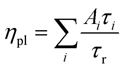 , where Ai is the sub-population fraction, τi is the excited state lifetime and τr is the radiative lifetime. For a ηpl of 70%, specified by the manufacturer, τr is 10.7 ns. In contrast, a 20 nm-thick QD film spin-cast on fused silica gives ηpl of 42% in an integrating sphere and mono-exponential PL decay with τ of 4.3 ns (Fig. 4a; Table 1, S/N 2). When the QD is spin-cast over an underlying polymer transport film, whether TFB, mTFF or PFOP, its lifetime is unchanged (Fig. 4b and c; Table 1, S/N 4, 6, 14). When a ZnMgO (Zn0.9Mg0.1O) layer is deposited over these, however, the QD film becomes less emissive, as evidenced by shortening of τ1 and drastic decrease of A1 (S/N 5 cf. 4; 12 cf. 6). The quenching of QD luminescence by ZnMgO has previously been noted.33–36 In contrast, when a polymer transport layer is overlaid, the τ of the QDs remains unchanged at 4.3 ns (S/N 10 cf. 6; 18 cf. 14). Thus, the polymer transport layers do not degrade the luminescent properties of the QD film, unlike ZnMgO. Possible contact with water during pickup also does not harm the QD film (S/N 8 cf. 6; 16 cf. 14). Nevertheless, the QD film itself slowly loses some ηpl over time, whether on fused silica (S/N 3 cf. 2), a polymer layer (S/N 7 cf. 6; 15 cf. 14), or sandwiched between polymer layers (S/N 11 cf. 10; 19 cf. 18). This loss is about 25% relative, even in a glovebox.
![[thin space (1/6-em)]](https://www.rsc.org/images/entities/char_2009.gif) exp(−t/τ1) + A2exp(−t/τ2). Correlation coefficient R2 is better than 0.995 in all cases. QD film thickness, 20 nm. Excitation, 374 nm; emission, 465 nm. For some samples, data were collected before and after 48 h storage in a nitrogen glovebox. S/N 1 gives the properties of the blue-emitting QD in octane solution (dispersion)
exp(−t/τ1) + A2exp(−t/τ2). Correlation coefficient R2 is better than 0.995 in all cases. QD film thickness, 20 nm. Excitation, 374 nm; emission, 465 nm. For some samples, data were collected before and after 48 h storage in a nitrogen glovebox. S/N 1 gives the properties of the blue-emitting QD in octane solution (dispersion)
| SN | Sample | A 1 | τ 1 (ns) | A 2 | τ 2 (ns) | Remarksa |
|---|---|---|---|---|---|---|
| a η pl is the photoluminescence efficiency of the QD. Relative change in ηpl of the QD film embedded in various structures is obtained by normalizing for the emission of the polymer underlayer and/or overlayer, which is taken to be stable with time. | ||||||
| 1 | QD soln, octane | 0.67 | 8.98 | 0.33 | 4.54 | η pl = 70%, manufacturer |
| 2 | Silica/QD, fresh | 1.00 | 4.34 | — | — | η pl = 42%, by integrating sphere |
| 3 | Silica/QD, after 48 h | 0.68 | 4.34 | 0.32 | 2.18 | η pl ≈ 85% of ‘fresh’ film (S/N 2) |
| 4 | TFB/QD, fresh | 0.17 | 4.6 | 0.83 | 0.64 | |
| 5 | TFB/QD/ZnMgO, fresh | 0.06 | 3.2 | 0.94 | 0.49 | |
| 6 | mTFF/QD, fresh | 0.51 | 4.45 | 0.49 | 0.72 | |
| 7 | mTFF/QD, after 48h | 0.40 | 4.2 | 0.60 | 0.73 | QD ηpl ≈ 60% of ‘fresh’ film (S/N 6) |
| 8 | mTFF/QD, water dip, fresh | 0.48 | 4.4 | 0.52 | 0.74 | |
| 9 | mTFF/QD, water dip, after 48 h | 0.33 | 4.2 | 0.67 | 0.70 | QD ηpl ≈ 55% of ‘fresh’ film (S/N 8) |
| 10 | mTFF/QD/PFOP, fresh | 0.35 | 4.4 | 0.65 | 0.70 | |
| 11 | mTFF/QD/PFOP, after 48 h | 0.28 | 4.3 | 0.72 | 0.70 | QD ηpl ≈ 70% of ‘fresh’ film (S/N 10) |
| 12 | mTFF/QD/ZnMgO, fresh | 0.19 | 3.3 | 0.81 | 0.74 | |
| 13 | mTFF/QD/ZnMgO, after 48 h | 0.13 | 3.0 | 0.87 | 0.58 | QD ηpl ≈ 60% of ‘fresh’ film (S/N 12) |
| 14 | PFOP/QD, fresh | 0.22 | 4.2 | 0.78 | 0.69 | |
| 15 | PFOP/QD, after 48 h | 0.19 | 3.9 | 0.81 | 0.71 | QD ηpl ≈ 75% of ‘fresh’ film (S/N 14) |
| 16 | PFOP/QD, water dip, fresh | 0.21 | 4.1 | 0.79 | 0.72 | |
| 17 | PFOP/QD, water dip, after 48 h | 0.18 | 3.9 | 0.82 | 0.68 | QD ηpl ≈ 85% of ‘fresh’ film (S/N 16) |
| 18 | PFOP/QD/mTFF, fresh | 0.29 | 4.2 | 0.71 | 0.72 | |
| 19 | PFOP/QD/mTFF, after 48 h | 0.25 | 4.1 | 0.75 | 0.72 | QD ηpl ≈ 80% of ‘fresh’ film (S/N 18) |
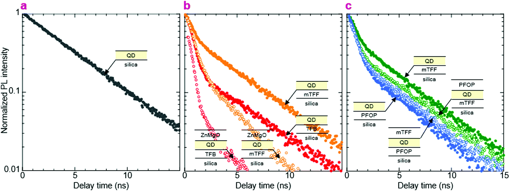 | ||
| Fig. 4 Time-resolved photoluminescence decay. Mesolight® blue-QDs (20 nm thick film): (a) on fused silica, (b) on the polymer HTL, before and after deposition of ZnMgO nanoparticles, (c) on the polymer HTL or ETL, before and after the lay down of the opposite transport layer. The fast component comes primarily from the polymer (τ ≈ 0.7 ns) and the slow component from the QDs (τ ≈ 4.3 ns in pristine film). Excitation, 374 nm; emission, 465 nm. | ||
Next, we elucidate from the systematic behavior of QLEDs with ZnMgO as the EIL but different HIL/HTL stacks that neither ZnMgO nor PEDT/TFB are good respective charge injection layers for the blue-QDs.
‘Standard’ PEDT/TFB/QD/ZnMgO/Al QLEDs
This is the design widely used in current research. Their JVL and η–J characteristics are shown in Fig. 5a, a few hours and about 10 days after fabrication. The characteristics show little current leakage below 2 V, less than 0.1 mA cm−2, indicating that the ZnMgO layer here is ‘optimal’, with similar behavior as aged films.37,38 The full-cycle sweep shows that electron injection improves in the returning half-cycle. This hysteresis is characteristic of the ZnMgO contact but often neglected in the literature. η reaches 3.5% at 8.0 V for 450 mA cm−2 and 10 kcd m−2. Both JV and η–J degrade with storage over days, but the decline in JV can be partly recovered by pre-biasing the QLED. Thus, electron injection by ZnMgO is unstable, and appears to be dependent on polarization. Related ageing characteristics have been discussed in the literature.35,36,39,40 The key feature here is that η–J also declines monotonically with time in storage. This points to a fundamental chemical incompatibility between ZnMgO and the blue-QDs.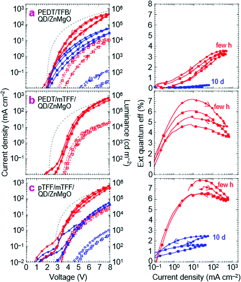 | ||
| Fig. 5 Blue-QLED characteristics for ZnMgO as the electron injection layer. Current density–voltage–luminance JVL (left), and external quantum efficiency η–J (right) of: (a) ITO/30 nm PEDT:PSSH/35 nm TFB/20 nm blue-QD/60nm ZnMgO/Al, (b) ITO/30 nm PEDT:PSSH/35 nm mTFF/20 nm blue-QD/60 nm ZnMgO/Al, (c) ITO/10 nm pTFF-C2F5SIS/35nm mTFF/20nm blue-QD/60 nm ZnMgO/Al. pTFF-C2F5SIS is hole doped. JVL plots: solid line, closed symbols (J), dashed line, open symbols (L); red (freshly made devices), blue (after storage). Every five data points shown. Two representative diodes shown in their second voltage sweep. Sweep protocol: 0 to +8 V then to −3 and back to 0 V. Grey dots: Mott–Gurney model with all interfaces Ohmic and neglecting diffusion current. | ||
To interpret the JV characteristics, we computed the ideal characteristics with only the drift current contribution in the Mott–Gurney approximation (see Methods).41 The model assumes Ohmic injection throughout the QLED with perfect recombination within the EML, incorporating carrier-density-dependent mobility (Fig. S2, ESI†).42,43 It has no free input parameters. The apparent built-in voltage V* is taken to be the true built-in potential Vbi given by 1/e × (ϕeff,1 − ϕeff,2), where ϕeff,i is the effective work function of each of the two contacts (1 = hole, 2 = electron).29 This approach enables simple comparison between the experimental results and space-charge-limited-conduction JV to determine whether at least one of the contacts is limiting, which is sufficient for our purpose, without detailed knowledge of all the contacts.
For this standard QLED, Vbi is expected to be 2.0 V, where ϕeff,1 for PEDT:PSSH is 5.2 eV, and ϕeff,2 for Zn0.9Mg0.1O is assumed to be 3.2 eV. While bulk ZnO(11![[2 with combining macron]](https://www.rsc.org/images/entities/char_0032_0304.gif) 0) has an electron affinity (EA) of 4.4 eV, ZnO nanoparticles can exhibit a work function as shallow as 3.5 eV, due to surface hydration,13,44 which may decrease to 3.2 eV at 10 mol% Mg doping through a CB shift.22,45 The computed ideal JV is approached by the experimental JV only at high voltages and in the reverse half-cycle. Since the PEDT/TFB contact is Ohmic,46 and so is ZnMgO/Al, this indicates an injection resistance into the QD EML. Experimentally, η–J falls to zero for J ≲ 1 mA cm−2 (V ≲ 3.2 V), suggesting that the current is highly imbalanced there.
0) has an electron affinity (EA) of 4.4 eV, ZnO nanoparticles can exhibit a work function as shallow as 3.5 eV, due to surface hydration,13,44 which may decrease to 3.2 eV at 10 mol% Mg doping through a CB shift.22,45 The computed ideal JV is approached by the experimental JV only at high voltages and in the reverse half-cycle. Since the PEDT/TFB contact is Ohmic,46 and so is ZnMgO/Al, this indicates an injection resistance into the QD EML. Experimentally, η–J falls to zero for J ≲ 1 mA cm−2 (V ≲ 3.2 V), suggesting that the current is highly imbalanced there.
Modified hole injection stacks
QLEDs with PEDT/mTFF or pTFF/mTFF as the hole injection stack give significantly improved results. Substituting TFB with mTFF produces a limiting contact at the PEDT/mTFF interface due to the injection barrier from PEDT to mTFF that frustrates buildup of a δ-doped interface there, particularly at low voltages.28,46 Indeed, JV yields an exponential-like behavior at low V (Fig. 5b). Yet η–J shows a higher η (6–7%) that peaks at a lower J (10 mA cm−2) at its exponentially rising portion, where the hole current is curtailed. The better resultant electron–hole recombination efficiency then indicates that electron injection by ZnMgO is previously limiting. The standard QLED suffers strong hole leakage at low V.A second substitution of PEDT with the ultrahigh-workfunction pTFF then turns the hole-injection stack Ohmic.18Vbi increases to 2.5 V, because ϕeff,1 increases to 5.7 eV, pinned just outside the VB edge of mTFF.18 The experimental JV matches the ideal one more closely and with less hysteresis than before. η–J broadens to give a quasi-plateau at ca. 7%, with a 90%-width spanning 10 to 100 mA cm−2. Clearly, the electron–hole recombination efficiency has improved considerably and over a wider current density range. Both JV and η–J at high V exceed those of the standard QLED. Thus, pTFF/mTFF clearly provides a better hole injection stack than PEDT/TFB, consistent with its energy-level diagram, where the VB edge of mTFF is better matched to the valence level of the QD. Then, through a feedback mechanism, this improves electron injection from the opposite contact. However, there is significant hole leakage through the ZnMgO layer at low V, and the standard QLED is hole-rich throughout operation.
Nevertheless, the JV of the improved QLED still decays to one-tenth of its initial value over 10 days, similar to the standard QLED, although its η–J decays less, to just one-quarter instead of one-tenth. In all cases, this η loss is irreversible, pointing to an underlying degradation of the QD layer. In general, QLED characteristics with ZnMgO contacts are highly variable, but the above trends are reproducible. See Fig. S3 (ESI†) for another set of devices fabricated months apart. Thus, it is clear that the ZnMgO/QD contact does not provide efficient electron injection into the blue-QD, especially at low voltages. Insertion of an ultrathin polymer dielectric layer could improve charge balance,33,47 but at the expense of increased tunnel resistance which may be mitigated using molecularly graded junctions demonstrated some time ago for polymer OLEDs.48,49
Double injection heterostructures: normal QLEDs
We next substitute the ZnMgO layer with N3/PFOP as the electron injection stack to give ITO/pTFF/mTFF/QD/PFOP/N3/Al QLEDs. The N3 layer is the EIL known to be capable of Ohmic electron injection into PFOP.30 The JVL and η–J characteristics of this QLED are shown in Fig. 6a. Despite having polymer transport layers sandwiching the QD film, electron–hole recombination occurs exclusively in the QD, as evidenced by pure QD electroluminescence (EL; Fig. 2e). Emission from the adjacent mTFF and PFOP layers (0 → 0 at 430 nm) has not been observed. This confirms the successful fabrication of a double type-I injection heterostructure.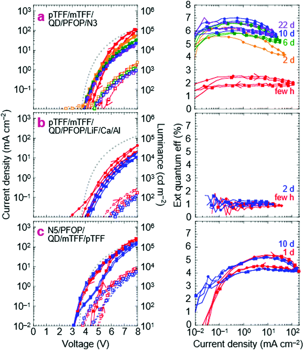 | ||
| Fig. 6 Blue-QLED characteristics for the double-type-I injection heterostructure. Current density–voltage–luminance JVL (left), and external quantum efficiency η–J (right) of: (a) ITO/10 nm pTFF-C2F5SIS/35 nm mTFF/20 nm blue-QD/60 nm PFOP/20 nm N3(Ox,AcO)/Al, (b) ITO/10 nm pTFF-C2F5SIS/35 nm mTFF/20 nm blue-QD/60 nm PFOP/3.5 nm LiF/10 nm Ca/Al, and (c) ITO/20 nm N5(Ox)/50 nm PFOP/20 nm blue-QD/35 nm mTFF/20 nm pTFF-C2F5SIS/Pd/Ag. pTFF-C2F5SIS is hole doped, N3 and N5 are electron doped. JVL plots: solid line, closed symbols (J), dashed line, open symbols (L); red (freshly made devices), blue (after storage). Every five data points shown. Two representative diodes shown in their second voltage sweep. Sweep protocol: 0 to +8 V then to −3 and back to 0 V. Grey dots: Mott–Gurney model with all interfaces Ohmic and neglecting diffusion current. | ||
With a Vbi of 3.15 V, from ϕeff,1 = 5.7 eV and ϕeff,2 = 2.55 eV, the ideal JV matches the experimental one fairly well. This confirms that introduction of PFOP ETL increases the electrical resistance as expected. However, η–J now exhibits a broad plateau with the 90%-width spanning four decades of current density from the diode turn-on of 10 μA cm−2, at 2% initially, improving to 6.5% over a few days. The initial η depression is not fully understood, but reproducible and appears related to an initial electron damage of the QDs, followed by subsequent healing (vide infra).
The successful flattening of η–J at the maximum η from the onset of diode turn-on confirms that balanced electron–hole injection can be enforced using the double-type-I device heterostructure. At the same time, the polymer transport layers ‘protect’ the QD sufficiently to improve the rest stability of the QLEDs. η–J does not decay with storage time, unlike for standard QLEDs. These results are reproducible. In another set of devices fabricated months later, the same η–J plateau is observed, stabilizing at 7.5–8% (Fig. S4a, ESI†). Furthermore, the strong electron injection stack, through the feedback effect, provides some latitude to employ a weaker hole injection stack, and conversely. This is illustrated by ITO/PEDT/TFB/QD/PFOP/N3/Al QLEDs, where the Al/N3/PFOP stack is able to coerce similar JV and η–J characteristics from PEDT/TFB as the pTFF/mTFF hole injection stack, though with the expected Vbi loss and the attendant low-V leakage (Fig. S4b, ESI†).
Substituting N3 with evaporated LiF produces a less optimal electron injection stack, reducing the electron current.30 Indeed, both JV and η–J decline, but η–J remains flat. This indicates that hole leakage into PFOP is still possible, consistent with the energy-level diagram that the hole transport level of PFOP is rather close to the valence level of the blue-QDs, about 0.1 eV. If the offset can be increased to 0.3 eV, complete blocking can be achieved.
Double injection heterostructures: inverted QLEDs
We also demonstrate inverted QLEDs where electrons are injected from a bottom ITO cathode, and holes from a top metal anode. A N5(Ox) layer was spin-cast on ITO–glass, followed by PFOP and blue-QD layers. An mTFF film was then picked up from water, a hole-doped pTFF-C2F5SIS layer was spin-cast, and Pd and Ag layers then evaporated sequentially. N5 has the same polyfluorene semiconductor core and work function as N3, but a higher ion density for improved adhesion to ITO.24,50 The JVL and η–J characteristics are shown in Fig. 6c. The JV in the return half-cycle is close to the ideal curve, indicating the absence of electron and hole barriers. However, the positive hysteresis indicates that electron injection at ITO/N5 may still be limiting in the forward half-cycle. This may not be surprising because of the large mismatch in work functions between ITO (4.5 eV) and N5 (2.55 eV), which would result in a large Schottky barrier that may be suppressed with further increase in doping. Nevertheless, the successful demonstration of inverted QLEDs points to the utility of the double-type-I heterostructure to coax carrier injection, even from non-traditional electrodes.A ‘white’ QLED
As a further check of the energy-level diagram, we fabricated another double-type-I QLED with ZnMgO/F8BT as the electron injection stack (Fig. S5, ESI†). A 10 nm-thick film of F8BT is used as the ETL by float-off and pick-up. F8BT has a VB edge at 5.9 eV, and CB edge estimated at 2.9 eV, with a transport gap similar or wider than that of the QD, but an emission gap much narrower due to excimer relaxation (λpeak, 540 nm; 2.3 eV).49 Hence, F8BT would not be able to inject electrons into the QD were its conduction level much higher than 2.9 eV. Then EL would only occur from F8BT since energy back transfer to the wider gap QD is not possible. Experimentally, EL occurs from both QD and F8BT layers, producing a ‘white’ spectrum. This confirms that the conduction level of the QD core is in the neighborhood of 2.9 eV. However, hole confinement is less effective here due to inefficient electron injection by ZnMgO into F8BT. Altogether, the device results support the energy-level diagram, and that elimination of ZnMgO is key to good storage stability.Emission modeling
In order to make an assessment of whether the best η reached here is consistent with perfect electron–hole recombination, we need to evaluate the effect of the photonic structure of the QLED on its emission rate and distribution. This is a well known topic in organic light-emitting diodes, where the emission rate and its distribution into air, trapped substrate and waveguide modes are governed by wave interference of the emitting dipole together with surface plasmon-polariton quenching by the metal electrode and other conductive layers.51,52 Thus, we employed the same theoretical framework based on the emitting-dipole formalism of Chance, Prock and Silbey to estimate radiative rates from the EML in the QLEDs.53There are two key parameters in this model, kr,o and knr,i, which are the hypothetical radiative decay rate under vacuum, and the intrinsic non-radiative decay rate in the film, respectively. These were evaluated and fixed by time-resolved photoluminescence measurements (see Methods). The photonic structure relevant to the double-type-I QLED is given in Fig. 7a; the optical properties of the layers are given in ESI,† Table S1. Then we computed kr and knr under the influence of the electrodes and other layers. These are given in Table 2 for the three key QLED structures—double-type-I normal QLED (A-1), double-type-I inverted QLED (B-1), and standard QLED (C-1). The example plot of photon emission rate as a function of emission angle illustrates why only a fraction of the emitted photons can escape into air, especially of the s-polarization (Fig. 7b). The example plots of kr and knr de-excitation rates with depth in the EML illustrate how knr for the out-of-plane emitting dipoles increases, but the radiative rate into air modes kr1 for in-plane emitting dipoles also increases, with decreasing distance to the metal layer (Fig. 7c). As a result, the radiative efficiency is marginally higher (8% relative) for the QD monolayer that is nearer to the metal electrode (Fig. 7d). These plots illustrate the sensitivity of η to the structure of the QLED and the location of the recombination zone.
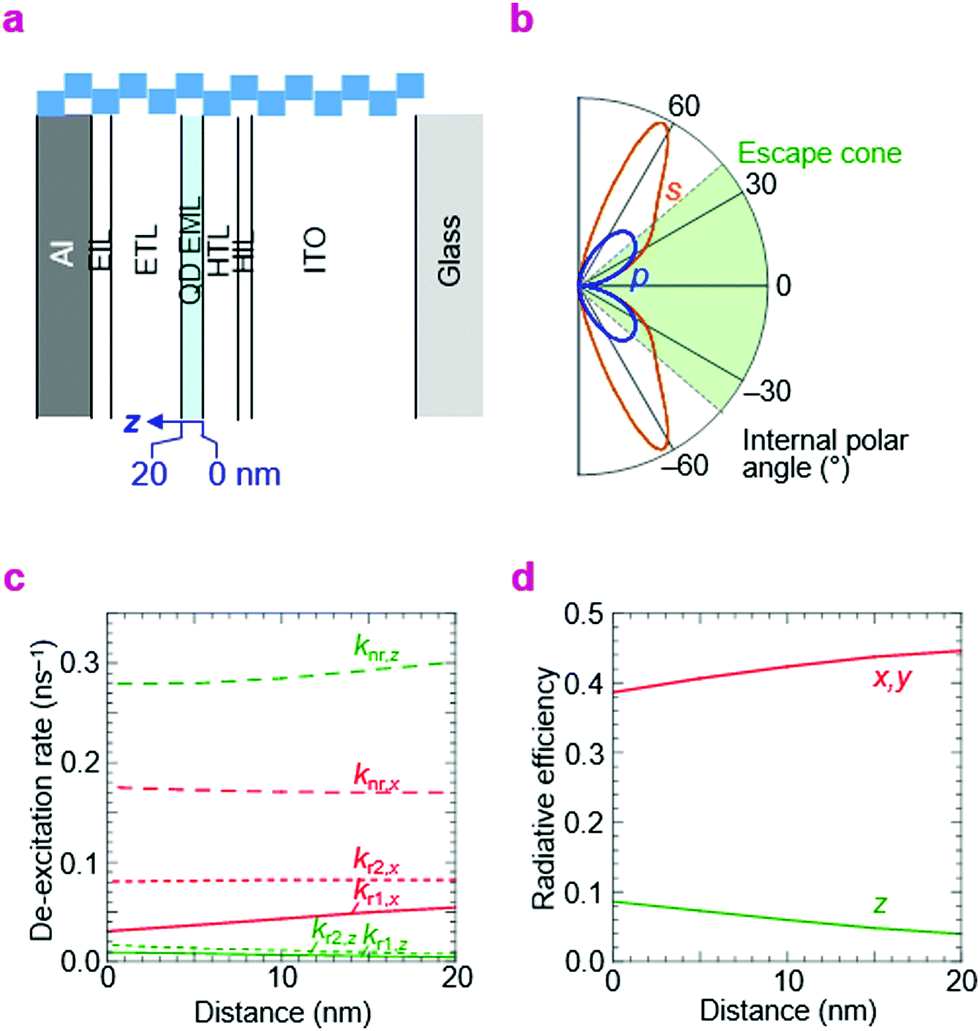 | ||
| Fig. 7 Computed radiative and non-radiative rates in QLEDs. (a) Photonic structure: glass/ITO/HIL/HTL/QD/ETL/EIL/Al (type A-1 of Table 2; bar length, 25 nm). (b) Integrated emission rate for s- and p-polarized photons as a function of internal polar angle. The emission is taken from an equal distribution of x-, y- and z-oriented dipoles, where the z-direction is perpendicular to the device plane. Photons emitted within the escape cone can exit the front face of the QLED. (c) Rate of de-excitation into various channels for z- and x-oriented dipoles as a function of distance z in the EML: non-radiative, nr; air radiative modes, r1; substrate radiative modes (glass and waveguide), r2. By symmetry, y-oriented dipoles behave identically as x-oriented dipoles. (d) Radiative efficiency of the z- and x-(or y-)dipole as a function of distance z. Emission wavelength, 470 nm. | ||
| SN | Device structurea | Radiative and non-radiative decay ratesb | Random dipolesc | Random degenerate dipolesd | |||||||
|---|---|---|---|---|---|---|---|---|---|---|---|
| k r1,x (ns−1) | k r2,x (ns−1) | k nr,x (ns−1) | k r1,z (ns−1) | k r2,z (ns−1) | k nr,z (ns−1) | EQEe | IQEf | EQEe | IQEf | ||
| a Device structure: A-1: Glass/150 nm ITO/10 nm HIL/35 nm HTL/20 nm QD/60 nm ETL/20 nm EIL/Al B-1: Glass/150 nm ITO/20 nm EIL/50 nm ETL/20 nm QD/35 nm HTL/20 nm HIL/Pd C-1: Glass/150 nm ITO/10 nm HIL/35 nm HTL/20 nm QD/60 nm ZnO/Al. b k r1 is the radiative decay rate into air modes, kr2 is the radiative decay rate into substrate modes—both glass and waveguide, knr is the non-radiative decay rate; subscripts x and z refer to x- and z-oriented radiating dipoles, respectively, y-oriented dipoles behave identically as x-oriented ones, by symmetry. Input parameters: The free-space radiative rate kr,o is taken to be 0.067 ns−1 (i.e. for n = 1.00) in order to reproduce the experimental kr of 0.093 ns−1 in octane (n = 1.41), corresponding to the radiative lifetime of 10.7 ns. The intrinsic non-radiative rate knr,i is taken to be 0.140 ns−1 (i.e., in the film state) to reproduce the excited state lifetime and PL quantum yield in a 20 nm-thick film on fused silica (exptal, 4.3 ns and 42%; theo, 4.2 ns and 35%). Emission wavelength, 470 nm. c Equal distribution of x, y and z-oriented non-degenerate emitting dipoles. d Equal distribution of xy, yz and xz doubly-degenerate emitting dipoles. e Theoretical radiative efficiency for air modes, given by: 2/3 × kr1,x/(kr1,x + kr2,x + knr,x) +1/3 × kr1,z/(kr1,z + kr2,z + knr,z), for randomly oriented, non-degenerate dipoles, and 1/3 × kr1,x/(kr1,x + kr2,x + knr,x) + 2/3 × (kr1,x + kr1,z)/(kr1,z + kr2,z + knr,z), for randomly oriented, doubly-degenerate dipoles. f Theoretical radiative efficiency for all modes, given by: 2/3 × (kr1,x + kr2,x)/(kr1,x + kr2,x + knr,x) + 1/3 × (kr1,z + kr2,z)/(kr1,z + kr2,z + knr,z), for randomly oriented, non-degenerate dipoles, and 1/3 × (kr1,x + kr2,x)/(kr1,x + kr2,x + knr,x) + 2/3 × (kr1,x + kr2,x + kr1,z + kr2,z)/(kr1,x + kr2,x + knr,x + kr1,z + kr2,z + knr,z), for randomly oriented, doubly-degenerate dipoles. | |||||||||||
| 1 | A-1 | 0.043 | 0.082 | 0.170 | 0.007 | 0.011 | 0.285 | 0.105 | 0.302 | 0.104 | 0.300 |
| 2 | B-1 | 0.055 | 0.065 | 0.163 | 0.003 | 0.040 | 0.279 | 0.133 | 0.328 | 0.129 | 0.321 |
| 3 | C-1 | 0.045 | 0.087 | 0.194 | 0.006 | 0.013 | 0.352 | 0.098 | 0.288 | 0.096 | 0.280 |
The results indicate for the blue-QDs used, the internal and external QEs are limited to 30% and 10%, respectively, for both A-1 and C-1 structures, but 30% and 13%, respectively, for the B-1 structure, provided that non-emissive states are absent. The photon outcoupling factor turns out to vary narrowly over 35–40%. However, since a dark state is known to occur with ageing of the QD film which reduces ηpl by about 20–25%, the theoretical maximum η is reduced correspondingly to 7.5–8%. Consequently, the experimental yield of 7–8% indicates that those QLEDs indeed exhibit near perfect electron–hole recombination efficiency. If these dark states can be completely eliminated, however, and knr,i reduced to 0.008 ns−1, the maximum attainable η would be 18%.
Stability issues
Numerous challenges have to be addressed in QLEDs. The application of the double-type-I heterostructure resolves the problem of balancing electron–hole injection and enforcing perfect recombination inside the QD EML. The use of polymer organic semiconductor transport layers resolves the problem of chemical incompatibility with ZnMgO. But several other issues still remain. Despite improved electron–hole balance, the operational lifetimes of these QLEDs in fact decrease. Here, we briefly outline some issues clarified or exposed by the new injection heterostructures.First, we show by luminescence spectroscopies that the ZnMgO layer chemically degrades both the QD and HTL over time, which can be avoided by polymer transport layers. PL quenching can already be observed in τ and ηpl measurements after film deposition, as noted earlier. With further stress bias or ageing, the standard QLEDs, but not the double-type-I QLEDs with polymer transport layers, exhibit a red-shift and broadening of their EL spectrum (Fig. 8a). The EL spectra of the latter remain pure with electrical driving in both normal and inverted architectures. Moreover, the standard QLEDs show that their PL spectra are strongly degraded beyond recognition after a few months, regardless of the polymer HTL (Fig. 8b). The HTL emission is completely changed, while the QD emission is greatly attenuated. In contrast, the double-type-I QLEDs show unchanged PL spectra. Regardless of whether the diode is fresh, aged (for five months), or driven to half-initial-luminance by constant current drive, the PL emission from the transport layers in: pTFF/mTFF/QD/PFOP/N3/Al, PEDT/TFB/QD/PFOP/N3/Al, and pTFF/mTFF/QD/PFOP/LiF/Ca/Al devices remains practically unchanged, although that from the QD layer does decrease significantly (Fig. 8c). Thus, ZnMgO is not chemically compatible with the QDs nor the polymer HTL, and the QDs show greater vulnerability than the transport polymers to electrical injection.
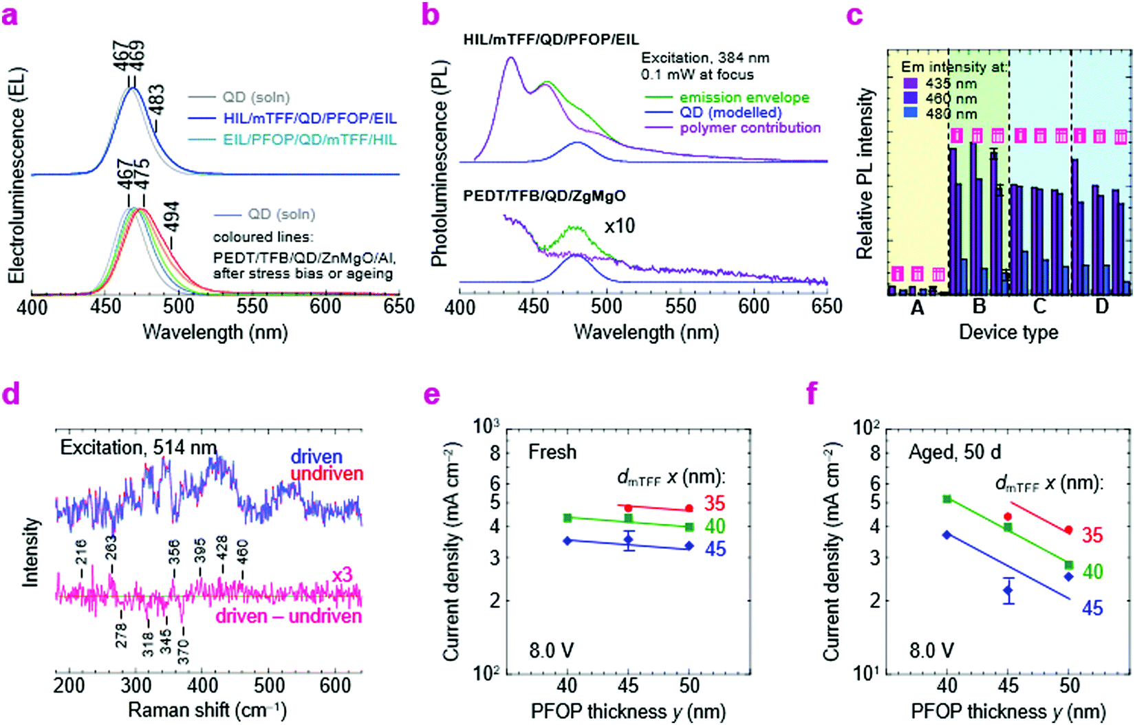 | ||
| Fig. 8 Stability analysis. (a) Comparative EL spectra. Emission from PEDT/TFB/QD/ZnMgO diodes exhibits red-shift with stress bias and aging. (b) Comparative PL spectra after five months; bottom panel expanded by 10×. Emission from PEDT/TFB/QD/ZnMgO diodes is degraded even when at rest. (c) Relative PL intensity: 435 and 460 nm, from the polymer; 480 nm, from QDs, for (i) the device after freshly evaporating Al, (ii) the device after long storage, and (iii) the device after stress-to-half-initial-luminance followed by long storage, for device type: (A) PEDT/TFB/QD/ZnMgO/Al, (B) HIL/mTFF/QD/PFOP/EIL/Al, (C) PEDT/TFB/QD/PFOP/EIL/Al, and (D) HIL/mTFF/QD/PFOP/LiF/Ca/Al. (d) Raman spectra of HIL/mTFF/QD/PFOP/EIL diodes before (undriven) and after stress-to-half-initial-luminance (driven). Sensitivity of ITO/20 nm pTFF/x nm mTFF/20 nm blue-QD/y nm PFOP/20 nm N3/Al to x and y: (e) a few hours after fabrication, (f) 50 days later. Error bar indicates typical population standard deviation. | ||
Next, we show by in situ Raman spectroscopy that this vulnerability is associated with chemical changes in the QD layer. Recent work has already indicated that CdZnSeS/ZnS core/shell QDs are damaged by electron injection.3 After driving to half-initial-luminance, the pTFF/mTFF/QD/PFOP/N3/Al QLED exhibits subtle changes in the 200–500 cm−1 region that indicate structural changes and formation of new inorganic chemical species (Fig. 8d). These sensitive measurements were made by comparing a driven diode with an adjacent undriven one. The following tentative assignments may be made: loss at 278 and 345cm−1, loss of ZnS; gain at 216 and 460 cm−1, formation of sulfur clusters;54 gain at 263 cm−1, selenium clusters.55 The gain at 356, 395 and 428 cm−1 may be attributed to ZnO clusters on account of its rich spectrum of modes.56 These molecular changes imply that under electron-rich conditions, the QD layer may undergo electrochemical reduction at its shell to release Zn, which then oxidizes to ZnO by scavenging adventitious O2 or H2O, counterbalanced by electrochemical oxidation to release sulfur and selenium. This is also consistent with the initially observed depression of η. The mechanism is reminiscent of the in device electrochemistry that occurs in doped conducting polymers under strong injection.57–59 Thus, future work would be required to attain better stabilization or passivation of the QDs to take full advantage of the new injection heterostructures.
Finally, we show that the polymer transport layers themselves also show a slow relaxation. To extract the layer contribution to ageing manifested by the slow decline in JV, we examined the variation of the QLED resistance with mTFF and PFOP layer thicknesses (dmTFF and dPFOP). The resistance initially varies little with dPFOP but more with dmTFF (Fig. 8e). After 50 days, the resistance increases considerably, and varies strongly with both dPFOP and dmTFF (Fig. 8f). This suggests that the space-charge voltage through both transport layers eventually becomes significant, pointing to a possible relaxation in the layers.
Afterword
The present work has demonstrated that the double-type-I charge-injection heterostructure with polymer organic semiconductors can indeed enforce near perfect electron–hole balance in the QD emitter layer over a wide current density range from the very onset of diode turn-on. Further optimization of energy levels and thicknesses should make it possible to further shift the JVL characteristic down-voltage by another few tenths of a volt. This overcomes a longstanding challenge, and at the same time, eliminates the destructive ZnMgO layer. As a consequence, we found that the QDs ironically become more unstable during operation, which appears to be a consequence of operando electrochemistry at the QD in the QLEDs. This work suggests the design of new polymer semiconductors as transport layers with more optimal energy levels and requisite processability from orthogonal solvents would be productive. This would enable simpler manufacturing by sequential film deposition. Suitable target solvents include those in the intermediate to strong polarity range, such as dimethyl sulfoxide, acetonitrile, N,N-dimethylformamide, 2,2,3,3,4,4,5,5-octafluoro-1-pentanol, tetrahydrofuran, diglyme and dimethyl carbonate (Fig. S6, ESI†). The QD films do not dissolve in these solvents, nor is their photoluminescence efficiency degraded. In the course of our work, we have also investigated small molecule organic semiconductors as ETLs, such as TSPO1 (Fig. S7, ESI†). Unfortunately, they appear to exhibit too low an electron mobility to be useful.Methods
Materials
1:6 w/w PEDT:PSSH (Clevios P VP Al 4083) was obtained from Heraeus Precious Metals; PFOP, mTFF and F8BT were obtained from Cambridge Display Technology; TFB (Mw 460k) from Xi’An Polymer; TSPO1 from Luminescence Technology Corp. All were used as received. Mesolight® blue-emitting quantum dots (ca. 100 mg mL−1 in octane) were obtained from Suzhou Xingshuo Nanotech Co. Ltd, and stored in a N2-glovebox prior to use. The solution was diluted with octane, if necessary. The blue-QD films were spin-cast in a glovebox. pTFF-C2F5SISNa was synthesized as reported by Ang et al.24,25 It was annealed at 120 °C for 1 h in a glovebox, then dissolved in anhydrous acetonitrile (ACN) to give a 100 mM solution. 0.9 equiv. of tris(4-bromophenyl)ammoniumyl hexachloroantimonate in anhydrous ACN (12 mM) was added to generate the hole-doped polymer solution. The solution was purified in the glovebox by dimethyl carbonate precipitation and ACN redissolution, twice, to give a self-compensated hole-doped polymer solution. Doped films were spin-cast in the glovebox. N3(Ox,AcO) and N5(Ox) were synthesized as reported by Tang et al.30In situ electron doping occurred during operation after device fabrication.30
Zn0.9Mg0.1O synthesis
0.90 mmol Zn(OAc)2·2H2O (99.999%, Sigma Aldrich) and 0.10 mmol Mg(OAc)2·4H2O (>99%, Sigma Aldrich) were dissolved in 10.0 mL of dimethyl sulfoxide (DMSO) in a 25 mL round-bottom flask, and stirred in air at room temperature until fully dissolved. 5.0 mL of anhydrous ethanol was added to 2.75 mmol of tetramethylammonium hydroxide (TMAH; Sigma Aldrich). 3.0 mL of this TMAH solution was added dropwise to the Zn–Mg solution at a rate of 0.1 mL min−1 under stirring at room temperature. The nanoparticles were precipitated with hexane, collected by centrifugation, and re-dispersed in anhydrous ethanol to a concentration of 25 mg mL−1.Float-off and pick-up film transfer method
A 40 nm-thick film of poly(diallyldimethylammonium chloride) was spin-cast onto clean glass substrates as the release layer. PFOP or mTFF was spin-cast from toluene solution over this film to give the desired thickness. The composite film on the substrate was then placed in a flat-bottom dish at a tilt angle of 15°. Millipore® water was pumped into the dish to increase its level at a rate of 50 μm s−1 to slowly float off the polymer semiconductor film. This film was then picked up by the device substrate wafer by inverting the device stack over the film and bringing them into contact. The film was then baked at 100 °C on a digital hotplate for 1 min in the glovebox.Device fabrication
PEDT:PSSH was filtered through a 0.45 μm nylon syringe filter and spin-cast in the ambient onto oxygen-plasma-cleaned ITO–glass substrates. The films were then baked at 140 °C on a digital hotplate for 10 min in a N2-glovebox. Alternatively, 10 nm-thick self-compensated hole-doped pTFF-C2F5SISNa films were spin-cast in the glovebox as the HIL (3 mM in ACN) onto the substrates. mTFF films were then spin-cast as the HTL (12 mg mL−1 in toluene) in the glovebox, and annealed at 110 °C on a digital hotplate for 5 min. Blue-QD films were then spin-cast as the EML (10 mg mL−1 in octane), and annealed at 100 °C for 5 min. ZnMgO films were then spin-cast (25 mg mL−1 in ethanol), and annealed at 80 °C for 5 min. Alternatively, PFOP films were deposited by the float-off and pick-up method in the ambient, as described above, then N3(Ox,AcO) films were spin-cast (1.8 mg mL−1 in a mixed solvent of 3:1 v/v 2,2,2-trifluoroethanol (TFE):2,2,3,3,4,4,5,5-octafluoro-1-pentanol (OFP)) in the glovebox. For inverted QLEDs: N5(TfO) films were spin-cast (2 mg mL−1 in the mixed solvent 3:1 v/v TFE:OFP) onto an oxygen-plasma-cleaned ITO–glass substrate, and then ion-exchanged with oxalate by contacting with a sodium oxalate solution (80 mM in 4:1 v/v H2O:methanol) in the ambient for 30 s before spin-off (6000 revolutions per minute (rpm)) and spin-rinse (H2O for 30 s, then spin-off 6,000 rpm) to give N5(Ox) as the precursor EIL. PFOP films were then spin-cast (7 mg mL−1 in toluene) in the glovebox, and annealed at 110 °C for 5 min. Blue-QD films were then deposited as before. mTFF films were then deposited by the float-off and pick-up method in the ambient, as described above, and annealed at 100 °C for 1 min in a glovebox. Self-compensated hole-doped pTFF-C2F5SISNa films were then spin-cast (6 mM in ACN). All films were annealed at 100 °C on the digital hotplate in the glovebox for 1 min before metal deposition. Metal films (Al, Pd or Ag as appropriate) were deposited by thermal evaporation through a shadow mask at a base pressure of 10−6 Torr to give eight 4.3 mm2 pixels on each device substrate.
Characterization
JVL characteristics were collected with a semiconductor parameter analyser (Keithley 4200), using a probe station with a calibrated Si photodiode in the N2-glovebox. Electroluminescence spectra were collected with a diode array spectrometer (Ocean Optics QE Pro). Photoluminescence spectra were collected using an excitation diode laser (384-nm wavelength, attenuated to 0.1 mW) focused by a parabolic mirror onto the QLED, with emission collected by the same parabolic mirror into a diode array spectrometer (Ocean Optics QE Pro). Time-resolved photoluminescence decay curves were collected using a spectrofluorometer (Horiba Fluorolog-3) at an excitation wavelength of 374 nm with a pulse width of 240 ps (LED), and emission wavelength of 465 nm. Raman spectra were collected using a Raman microscope (Renishaw) through a ×20 objective at 514 nm excitation with 1 mW at focus using a stepper motor to collect data averaged over an array of image points.JV modeling
Ideal JV characteristics were computed as the drift current contribution in the Mott–Gurney approximation for the ideal device model which assumes Ohmic injection throughout the entire QLED stack and perfect recombination within the EML. The relevant electron or hole mobility function of the polymer transport layer with carrier-density dependence was separately measured and used as input. The carrier mobility in the QD layer was assumed to be constant at 1 × 10⁻⁶ cm2 V−1 s−1 for both electrons and holes,1,2,33,40 while the ZnMgO layer was taken to be Ohmic with negligible resistance due to its high electrical conductivity (≳1 × 10⁻⁶ S cm−1).37Vbi was taken to be 1/e × (ϕeff,1 − ϕeff,2) for the contacts selected. Because the diffusion current contribution was neglected, these ideal JV characteristics would underestimate the true current in the vicinity of diode turn-on and below.Emission modeling
De-excitation rates were computed in the Chance, Prock and Silbey emitting-dipole formalism.53 First, kr,o was evaluated to reproduce the experimental τr of the blue-QD in octane (10.7 ns). Then knr,i was evaluated to reproduce both τ1 and ηpl of the 20 nm-thick blue-QD film on the fused silica substrate (4.3 ns and 42%, respectively). Results are given in footnote b of Table 2. Self-consistency was achieved. This validated the essential assumptions of the model that the radiative lifetime in the film is modified from that in solution through the photonic structure effect, while the excess PL quenching in the film can be treated as an additional competing decay channel. Then we computed the effects of the electrodes and other layers on kr and knr self-consistently, and the distribution of kr into its various propagating photon modes. The results are given in Table 2 separately for in-plane and out-of-plane emitting dipoles, and broken down into air modes and substrate modes. We performed the computations for the two cases of randomly oriented emitting dipoles: non-degenerate and doubly-degenerate. The emitting dipoles of ideal CdSe QDs are doubly degenerate, but the results here show that this does not really matter—the photonic structure effects are practically identical.Author contributions
L. X. W., C. G. T., Z. S. T. and H. Y. P. performed the device fabrication, together with materials and device characterisation. R. Q. P. and L. L. C. guided the work. L. L. C. led the materials research effort in polymer injection and transport layers. R. Q. P. led the device heterostructure research effort in QLEDs. P. K. H. H. provided theoretical support through current–voltage modeling and emission modeling. L. X. W., C. G. T., R. Q. P. and P. K. H. H. wrote the manuscript. All authors discussed the manuscript.Conflicts of interest
There are no conflicts to declare.Acknowledgements
We thank Qiu-Jing Seah and Mazlan Nur Syafiqah for synthesizing pTFF-C2F5SIS, N3(Ox,AcO) and N5(Ox) materials, and Desmond Teo for experimental support. Li-Xi Wang thank National Key Research and Development Program of China (2018YFE0125500, 2016YFB0401600), Natural Science Foundation of Jiangsu Province (BK20190774) and Postgraduate Research & Practice Innovation Program of Jiangsu Province (KYCX19_0082) for funding. This research is partially funded by the National Research Foundation, Prime Minister's Office, Singapore under its Competitive Research Programme (CRP Award No. NRF-CRP24-2020-0006: A-0008375-00-00, A-0008375-01-00).References
- Y. H. Won, et al., Highly efficient and stable InP/ZnSe/ZnS quantum dot light-emitting diodes, Nature, 2019, 575, 634–638 CrossRef CAS PubMed.
- T. Kim, et al., Efficient and stable blue quantum dot light-emitting diode, Nature, 2020, 586, 385–389 CrossRef CAS PubMed.
- C. Pu, et al., Electrochemically-stable ligands bridge the photoluminescence-electroluminescence gap of quantum dots, Nat. Commun., 2020, 11, 937 CrossRef CAS PubMed.
- J. M. Pietryga, et al., Spectroscopic and device aspects of nanocrystal quantum dots, Chem. Rev., 2016, 116, 10513–10622 CrossRef CAS PubMed.
- Y. Deng, et al., Deciphering exciton-generation processes in quantum-dot electroluminescence, Nat. Commun., 2020, 11, 2309 CrossRef CAS PubMed.
- F. Wang, et al., Suppressed efficiency roll-off in blue light-emitting diodes by balancing the spatial charge distribution, J. Mater. Chem. C, 2020, 8, 12927 RSC.
- Y. Shirasaki, G. J. Supran, W. A. Tisdale and V. Bulović, Origin of efficiency roll-off in colloidal quantum-dot light-emitting diodes, Phys. Rev. Lett., 2013, 110, 217403 CrossRef PubMed.
- W. K. Bae, et al., Controlling the influence of Auger recombination on the performance of quantum-dot light-emitting diodes, Nat. Commun., 2013, 4, 2661, DOI:10.1038/ncomms3661.
- J. H. Lim, Y. S. Park, K. F. Wu, H. J. Yun and V. I. Klimov, Droop-free colloidal quantum dot light-emitting diodes, Nano Lett., 2018, 6645–6653 CrossRef CAS PubMed.
- Y. Z. Sun, et al., Investigation on thermally induced efficiency roll-off: Toward efficient and ultrabright quantum-dot light-emitting diodes, ACS Nano, 2019, 13, 11433–11442 CrossRef CAS PubMed.
- W. Zou, et al., Minimising efficiency roll-off in high-brightness perovskite light-emitting diodes, Nat. Commun., 2018, 9, 608 CrossRef PubMed.
- C. Zou, Y. Liu, D. S. Ginger and L. Y. Lin, Suppressing efficiency roll-off at high current densities for ultra-bright green perovskite light-emitting diodes, ACS Nano, 2020, 14, 6076–6086 CrossRef CAS PubMed.
- V. Stevanović, S. Lany, D. S. Ginley, W. Tumas and A. Zunger, Assessing capability of semiconductors to split water using ionization potentials and electron affinities only, Phys. Chem. Chem. Phys., 2014, 16, 3706–3714 RSC.
- W. K. Bae, K. H. Char, H. Hur and S. H. Lee, Single-step synthesis of quantum dots with chemical composition gradients, Chem. Mater., 2008, 20, 531–539 CrossRef CAS.
- L. L. Chua, et al., Large damage threshold and small electron escape depth in X-ray absorption spectroscopy of a conjugated polymer thin film, Langmuir, 2006, 22, 8587–8594 CrossRef CAS PubMed.
- J. Zhang, et al., InP/ZnSe/ZnS quantum dots with strong dual emissions: visible excitonic emission and near-infrared surface defect emission and their application in in vitro and in vivo bioimaging, J. Mater. Chem. B, 2017, 5, 8152–8160 RSC.
- C.-Y. Han and H. Yang, Development of colloidal quantum dots for electrically driven light-emitting devices, J. Korean Ceram. Soc., 2017, 54, 449–469 CrossRef CAS.
- R. Q. Png, et al., Madelung and Hubbard interactions in polaron band model of doped organic semiconductor, Nat. Commun., 2016, 7, 11948, DOI:10.1038/ncomms11948.
- Q. Sun, et al., Bright, multicoloured light-emitting diodes based on quantum dots, Nat. Photon., 2007, 1, 717–722 CrossRef CAS.
- W. Cao, et al., Highly stable QLEDs with improved hole injection via quantum dot structure tailoring, Nat. Commun., 2018, 9, 1–6 CrossRef CAS PubMed.
- L. Qian, Y. Zheng, J. Xue and P. H. Holloway, Stable and efficient quantum-dot light-emitting diodes based on solution-processed multilayer structures, Nat. Photonics, 2011, 5, 543–548 CrossRef CAS.
- J. H. Kim, et al., Performance improvement of quantum-dot-light-emitting diodes enabled by an alloyed ZnMgO nanoparticle electron transport layer, Chem. Mater., 2014, 27, 197–204 CrossRef.
- S. Wang, et al., Bandgap tunable Zn1–xMgxO thin films as electron transport layers for high performance quantum dot light-emitting diodes, J. Mater. Chem. C, 2017, 5, 4724 RSC.
- M. C. Y. Ang, et al., Spectator cation size effect on the work function and stability of self-compensated hole-doped polymers, J. Mater. Chem. C, 2020, 2019, 124–131 RSC.
- A. G. Ricciardulli, et al., Polymer-perovskite blend light-emitting diodes using a self-compensated heavily doped polymeric anode, APL Mater., 2020, 8, 021101 CrossRef CAS.
- C. G. Tang, et al., Doped polymer semiconductors with ultrahigh and ultralow work functions for ohmic contacts, Nature, 2016, 539, 536–540 CrossRef CAS PubMed.
- Q. M. Koh, et al., Overcoming the water oxidative limit for ultra-high-workfunction hole-doped polymers, Nat. Commun., 2021, 12, 3345 CrossRef CAS PubMed.
- M. Zhou, et al., The role of delta-doped interfaces for Ohmic contacts to organic semiconductors, Phys. Rev. Lett., 2009, 103, 036601–036604 CrossRef PubMed.
- M. Zhou, et al., Effective work functions for the evaporated metal/organic semiconductor contacts from in-situ diode flatband potential measurements, Appl. Phys. Lett., 2012, 101, 013501 CrossRef.
- C. G. Tang, et al., Multivalent anions as universal latent electron donors, Nature, 2019, 573, 519–525, DOI:10.1038/s41586-019-1575-7.
- J. Song, et al., A general method for transferring graphene onto soft surfaces, Nat. Nanotechnol., 2013, 8, 356–362 CrossRef CAS PubMed.
- J. G. Yang, F. Y. Kam and L. L. Chua, Transferred metal electrode films for large-area electronic devices, Appl. Phys. Lett., 2014, 105, 193304 CrossRef.
- X. Dai, et al., Solution-processed, high-performance light-emitting diodes based on quantum dots, Nature, 2014, 515, 96–99 CrossRef CAS PubMed.
- K. Acharya, et al., High efficiency quantum dot light emitting diodes from positive aging, Nanoscale, 2017, 14451–14487 RSC.
- Q. Su, Y. Sun, H. Zhang and S. Chen, Origin of positive aging in quantum-dot light-emitting diodes, Adv. Sci., 2018, 5, 1800549 CrossRef PubMed.
- S. Chen, et al., On the degradation mechanisms of quantum-dot light-emitting diodes, Nat. Commun., 2019, 10, 765 CrossRef CAS PubMed.
- W. J. Zhang, et al., Positive aging effect of ZnO nanoparticles induced by surface stabilization, J. Phys. Chem. Lett., 2020, 11, 5863–5870 CrossRef CAS PubMed.
- M. Chrzanowski, G. Zatryb, P. Sitarek and A. Podhorodecki, Effect of air exposure of ZnMgO nanoparticle electron transport layer on efficiency of quantum-dot light-emitting diodes, ACS Appl. Mater. Interfaces, 2021, 13, 20305–20312 CrossRef CAS PubMed.
- S. Ding, et al., Impact of resistive switching effects in ZnMgO electron transport layer on the aging characteristics of quantum dot light-emitting diodes, Appl. Phys. Lett., 2020, 117, 093501 CrossRef CAS.
- X. L. Xue, et al., Degradation of quantum dot light emitting diodes, the case under a low driving level, J. Mater. Chem. C, 2020, 8, 2014–2018 RSC.
- J. A. Röhr, D. Moia, S. A. Haque, T. Kirchartz and J. Nelson, Exploring the validity and limitations of the Mott–Gurney law for charge-carrier mobility determination of semiconducting thin-films, J. Phys.: Condens. Matter, 2018, 30, 105901 CrossRef PubMed.
- C. Tanase, P. W. M. Blom and D. M. De Leeuw, Origin of the enhanced space-charge-limited current in poly(p-phenylene vinylene), Phys. Rev. B, 2004, 70, 193202 CrossRef.
- C. Zhao, et al., Improving organic photovoltaic cells by forcing electrode work function well beyond onset of Ohmic transition, Nat. Commun., 2021, 12, 2250 CrossRef CAS PubMed.
- S. Gutmann, M. Conrad, M. A. Wolak, M. M. Beerbom and R. Schlaf, Work function measurements on nano-crystalline zinc oxide surfaces, J. Appl. Phys., 2012, 111, 123710 CrossRef.
- Y. Ke, et al., Enhanced electron mobility due to dopant-defect pairing in conductive ZnMgO, Adv. Funct. Mater., 2014, 24, 2875–2882 CrossRef CAS.
- M. Zhou, et al., Determination of the interface delta-hole density in a blue-emitting organic semiconductor diode by electromodulated absorption spectroscopy, Appl. Phys. Lett., 2010, 97, 113505 CrossRef.
- H. Zhang, et al., Ultrastable quantum-dot light-emitting diodes by suppression of leakage current and exciton quenching processes, ACS Appl. Mater. Interfaces, 2016, 8, 31385–31391 CrossRef CAS PubMed.
- P. K. H. Ho, M. Granström, R. H. Friend and N. C. Greenham, Ultrathin self-assembled layers at the ITO interface to control charge injection and electroluminescence efficiency in polymer light-emitting diodes, Adv. Mater., 1998, 10, 769–774 CrossRef CAS.
- P. K. H. Ho, et al., Molecular-scale interface engineering for polymer light-emitting diodes, Nature, 2000, 404, 481–484 CrossRef CAS PubMed.
- M. C. Y. Ang, et al., Bulk Ion-clustering and surface ion-layering effects on work function of self-compensated charge-doped polymer semiconductors, Mater. Horiz., 2020, 7, 1073–1082 RSC.
- J. S. Kim, P. K. H. Ho, N. C. Greenham and R. H. Friend, Electroluminescence emission pattern of organic light-emitting diodes: Implications for device efficiency calculations, J. Appl. Phys., 2000, 88, 1073–1081 CrossRef CAS.
- L. H. Smith, J. A. E. Wasey, I. D. W. Samuel and W. L. Barnes, Light out-coupling efficiencies of organic light-emitting diode structures and the effect of photoluminescence quantum yield, Adv. Funct. Mater., 2005, 15, 1839–1844 CrossRef CAS.
- R. R. Chance, A. Prock and R. Silbey, in Advances in Chemical Physics, ed. I. Prigogine and S.A. Rice, John Wiley & Sons, 1978, vol. 37 Search PubMed.
- L. J. Zhang, et al., Chain breakage in the supercooled liquid–liquid transition and re-entry of the λ-transition in sulfur, Sci. Rep., 2018, 8, 4558 CrossRef PubMed.
- A. H. Goldan, et al., Molecular structure of vapor-deposited amorphous selenium, J. Appl. Phys., 2016, 120, 135101 CrossRef.
- C. Morales, A. del Campo, J. Méndez, P. Prieto and L. Soriano, Re-oxidation of ZnO clusters grown on HOPG, Coatings, 2020, 10, 401 CrossRef CAS.
- P. J. Chia, et al., Injection-induced de-doping in a conducting polymer during device operation: Asymmetry in thoe hole injection and extraction rates, Adv. Mater., 2007, 19, 4202–4207 CrossRef CAS.
- D. Belaineh, et al., A high-performance p-doped conducting polymer blend based on sulfonated polyalkoxythiophene and poly(4-hydroxystyrene), Chem. Mater., 2014, 26, 4724–4730 CrossRef CAS.
- C. Zhao, et al., Bias-induced electrochemical electron doping of organic semiconductor contacts, Adv. Mater. Interfaces, 2019, 6, 1900607 CrossRef CAS.
Footnotes |
| † Electronic supplementary information (ESI) available. See DOI: https://doi.org/10.1039/d1mh00859e |
| ‡ These authors contributed equally to this work. |
| This journal is © The Royal Society of Chemistry 2022 |