
 Open Access Article
 This Open Access Article is licensed under a
 Creative Commons Attribution 3.0 Unported Licence
Revealing the origin of magnetoresistance in unipolar amorphous organic field-effect transistors†
Carolin
Isenberg
and
Tobat P. I.
Saragi
*
Department of Mathematics and Science and Center for Interdisciplinary Nanostructure Science and Technology (CINSaT), University of Kassel, Heinrich-Plett-Straße 40, D34132 Kassel, Germany. E-mail: tobat.saragi@uni-kassel.de
First published on 27th August 2014
Abstract
We report on the magnetoresistance (MR) effect in a unipolar p-channel field-effect transistor based on amorphous thin film of low molecular weight 2,2′,7,7′-tetrakis(diphenylamino)-9,9′-spirobifluorene (Spiro-TAD). To scrutinize the origin of this effect two themes have been studied: (i) the influence of gate dielectric SiO2 surface treatment and (ii) the importance of organic molecular p-dopant 1,3,4,5,7,8-hexafluorotetracyanonaphthoquinodimethane (F6-TNAP) thin films sandwiched between SiO2 and Spiro-TAD. A device fabricated on bare SiO2 shows larger MR than one fabricated on hexamethyldisilazane-treated SiO2, suggesting the bipolaron species as the origin of this effect. This could be understood through two aspects. (i) The stabilization of bipolaron, i.e. trapped charge-stabilized bipolaron. Due to large energy cost for bipolaron formation, the stabilization of bipolaron by a trap with opposite sign is favored. Additionally, interface doping of Spiro-TAD with F6-TNAP reveals a significant enhancement in MR caused by an increase in trap density and charge carriers, boosting the effectiveness of bipolaron stabilization. (ii) Larger energetic disorder that might compensate the energy cost for bipolaron formation is expected to be obtained for a device fabricated on bare SiO2 caused by dipolar disorder at the corresponding interface. Adding a thin layer of F6-TNAP is expected to increase the energetic disorder as well.
1. Introduction
Organic semiconductors have attracted much interest in the scientific community since the first report on high conductivity in the conjugated polymer cis-polyacetylene doped with AsF5.1 This research field has been extensively studied over more than three decades, leading to a new research area called “organic electronics”. The applications of organic π-conjugated molecules or polymers can already be found in light-emitting devices,2 solar cells,3 and field-effect transistors.4Along with optoelectronic devices, the field of spin-transport electronics, so-called spintronics, is a blossoming research field as well. Research in spintronics has been carried out for many material systems such as metals, ferromagnets and semiconductors.5 Thus, one may think to utilize thin films of organic π-conjugated molecules and polymers as spacers or tunnel barriers in spintronic devices due to the abundance of physical aspects and potential practical applications. Interest has rapidly increased, triggered by the first observation of giant magnetoresistance (MR; MR = ΔR/R, where ΔR is the resistance of the sample in an external magnetic field minus the resistance of the sample in the absence of external magnetic field, R) in an organic spin-valve measured at low temperatures.6
Generally, two types of devices have been reported. Firstly is a device consisting of an organic semiconductor as a spacer in a so-called organic spin-valve embedded between two ferromagnetic electrodes with different coercive fields: 1st ferromagnet/organic spacer/2nd ferromagnet. In this case MR is caused by a change in the resistance due to a change in the mutual orientation of the magnetizations of the two ferromagnetic electrodes, demonstrating a possibility for injecting, transporting and detecting a non-equilibrium spin current.7–9 Secondly, MR effect has also been observed and obtained in an organic light-emitting diode (OLED) with a structure of non-magnetic anode/organic spacer/non-magnetic cathode, which has been dubbed an organic magnetoresistance (OMAR) device.10 Generally, the effect occurs at room temperature and is significantly large at low external magnetic field.10 Ease of and simple fabrication of this device as for conventional OLEDs or organic solar cells have motivated intensive research activity in the scientific community. Both magnetoconductance of >25% and magneto-electroluminescence of over 50% have been reported and measured at room temperature and at low external magnetic field.11 Also, several efforts have been recently devoted to investigating MR in conductive polymers and their nanocomposites.12–17
So far OMAR has been observed in two-terminal devices like OLEDs or organic solar cells. The corresponding microscopic mechanism can be attributed to the interaction between spin-carrying particles. The hyperfine interaction is generally accepted as the source that affects the spin dynamic in organic semiconductors and is, therefore, responsible for the MR effect at low external magnetic fields. However, no consensus can be reached at the moment as to which pairs of quasi particles influence the resistance or the current in organic devices. The specific interaction between spin-carrying particles in OMAR is still a big scientific puzzle and is debated among scientists, resulting in several existing theories such as excitonic model,18,19 triplet–polaron interaction (TPI) model20 or bipolaron model.21 The excitonic model is based on the spin-dependent formation of electrostatically bound polaron pairs formed from oppositely injected current (two-carrier process), whereas the bipolaron model describes the spin-dependent formation of two equally charged polarons (one-carrier process). The TPI model describes the capturing of a polaron by long-lived triplet excitons for which an applied magnetic field influences the number of triplet excitons. Recently, the importance of traps and trion species as origins of OMAR has been proposed and considered.22 Also, a call for more specific investigation of organic spin-valves and OMAR has been debated among scientists, including a comprehensive theme such as device physics, modelling, spectroscopy study and design and synthesis of new materials.23
We realize that this field is quite complex especially for two-terminal devices and, therefore, there is an urgent need to extend the study of OMAR in three-terminal devices like field-effect transistors. In this device geometry the sign of charge carriers is defined by the gate voltage and the mobility and charge carrier density can be determined independently, which are the unique characteristics in comparison to a diode. Furthermore, a field-effect transistor also allows for much control of the charge carrier density through the third electrode. However, there is not much information to be found in the literature about magnetic field effects in organic field-effect transistors (OFETs) without ferromagnetic electrodes.24 Our group has intensively studied the OMAR effects in OFETs measured at room temperature and at low external magnetic field.25–29 MR in OFETs has been observed in two different material systems and experimental conditions: (i) photoinduced MR in p-channel OFETs based on acene compounds25–27 and (ii) MR in bipolar material systems such as in a binary mixture composed of electron donor and acceptor and bipolar molecular glass.28,29
Here, we scrutinize the OMAR effects by isolating a certain mechanism and report MR effects in a unipolar (p-channel) field-effect transistor based on low molecular weight 2,2′,7,7′-tetrakis(diphenylamino)-9,9′-spirobifluorene (Spiro-TAD).30,31 We also found that the MR effect is strongly influenced by surface treatment of the corresponding SiO2 gate dielectric. Finally, the influence of an additional thin layer of the organic molecular p-dopant 1,3,4,5,7,8-hexafluorotetracyanonaphthoquinodimethane (F6-TNAP) deposited between SiO2 and Spiro-TAD on the MR effects is presented and discussed in detail. Spiro-TAD and F6-TNAP have been chosen for this study for the following reasons: (i) vacuum-evaporated thin films of Spiro-TAD showed smooth surface and the corresponding transistor characteristics did not change when the samples were placed in ambient atmosphere for nine months32 and (ii) F6-TNAP has been used as p-dopant in a hole transport layer in OLEDs.33,34
2. Results and discussion
2.1. The influence of surface-treated gate dielectric
A schematic view of our bottom-contact field-effect transistor and the chemical structures of Spiro-TAD and F6-TNAP, including their energy levels, are displayed in Fig. 1. | ||
| Fig. 1 (a) Schematic view of a bottom-contact OFET with a bilayer thin film of F6-TNAP and Spiro-TAD. The thickness of Spiro-TAD was kept constant at 40 nm, whereas the thickness of F6-TNAP was varied between 0 and 15 nm. In this study two types of SiO2 were used: bare SiO2 and hexamethyldisilazane (HMDS)-treated SiO2 gate dielectric. (b) The chemical structures of Spiro-TAD and F6-TNAP. (c) Energy level diagrams of Spiro-TAD,34 F6-TNAP34 and gold.35 | ||
Firstly, we investigated the influence of surface-treated gate dielectric on the MR in a unipolar field-effect transistor particularly for the commonly used gate dielectric silicon dioxide (SiO2). For this purpose we employed SiO2 with two different surface treatments, namely bare SiO2 and hexamethyldisilazane (HMDS)-treated SiO2 substrates (see Experimental section for details). In organic electronics HMDS is one of the most frequently used monolayers on the SiO2 gate dielectric for OFETs and is a silane with short chain length and high vapor pressure so that we can deposit it on hydroxylated surfaces of SiO2 from the vapor phase by heating under vacuum.
Fig. 2a–c show the output and transfer curves of unipolar Spiro-TAD field-effect transistors utilizing bare SiO2 and HMDS-treated SiO2. As expected, higher drain current Id is obtained for the device fabricated on HMDS-treated SiO2 with respect to that on bare SiO2, which is commonly observed in organic electronics. In this case, HMDS molecules replace a fraction of the surface silanol (SiOH) groups with –O–Si–CH3 groups, which provide a barrier to prevent carrier trapping of negative charges on the residual silanol groups. On the contrary, the MR experiments show that the MR values achieved for a device fabricated on bare SiO2 are much higher (∼0.023%) than that on HMDS-treated SiO2 (a negligible MR of <0.01%), as depicted in Fig. 2d. Furthermore, MR effects and values for devices fabricated on bare SiO2 and HMDS-treated SiO2 have been checked for several devices and at different voltages (Fig. S1 and S2†). Based on our experiment and observation we conclude that significant MR is obtained for devices employing bare SiO2 and, in contrast, a negligible effect is achieved for devices fabricated on HMDS-treated SiO2. The absence of the MR effect was also reported for other spiro-linked compound field-effect transistors fabricated on HMDS-treated SiO2.28
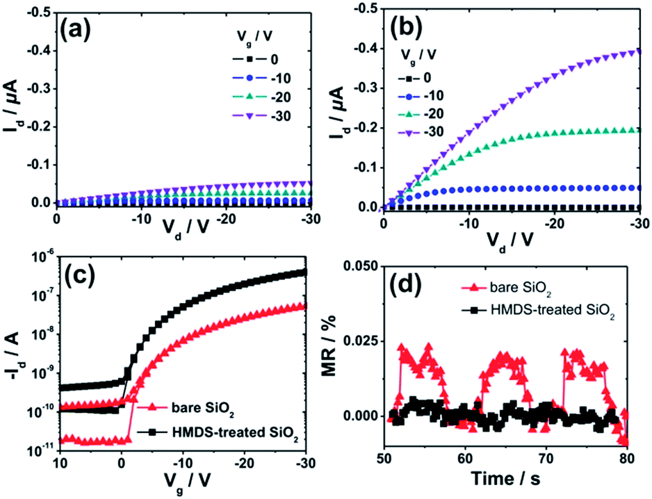 | ||
| Fig. 2 Output curves of Spiro-TAD field-effect transistors fabricated on (a) bare SiO2 and (b) HMDS-treated SiO2. (c) The corresponding transfer curves were recorded at Vd = −30 V. (d) The MR effects of both devices were measured at Vd = Vg = −40 V (for bare SiO2) and Vd = Vg = −50 V (for HMDS-treated SiO2). | ||
2.2. The role of interface doping with organic molecular p-dopant
To further study the reliability of our findings we deposited an additional thin film of 5 nm thick organic molecular p-dopant F6-TNAP directly on bare SiO2 and on HMDS-treated SiO2. We found that the Id of the device fabricated on HMDS-treated SiO2 is higher than that of the device on bare SiO2, as displayed in Fig. 3a. Here, we mention that no transistor action could be observed in devices fabricated with pristine F6-TNAP in the measurement range of our set-up (−100 V ≤ Vg and Vd ≤ +100 V), which is probably due to the energy level mismatch between the work function of gold and the lowest unoccupied molecular orbital of F6-TNAP. However, interesting results were observed in MR experiments. In the case of F6-TNAP deposited between SiO2 and Spiro-TAD, the MR values obtained for devices fabricated on bare SiO2 are higher than those fabricated on HMDS-treated SiO2 (see Fig. 3b). Also, MR in the device fabricated on HMDS-treated SiO2 with an additional thin layer of F6-TNAP is higher than that without F6-TNAP (compare Fig. 2d and 3b). In this case, a MR of 0.01–0.02% is obtained for devices fabricated on HMDS-treated SiO2, whereas a MR of ∼0.05% is achieved for devices fabricated on bare SiO2, as displayed in Fig. 3b.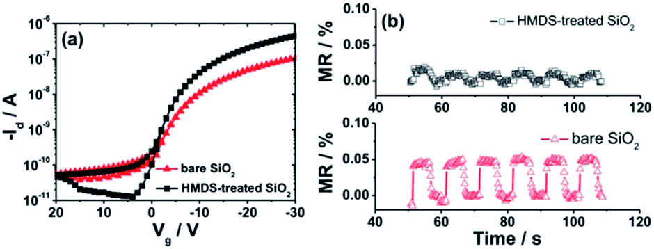 | ||
| Fig. 3 (a) Transfer characteristics of bilayer F6-TNAP (5 nm)/Spiro-TAD (40 nm) field-effect transistors fabricated on bare SiO2 and HMDS-treated SiO2 measured at Vd = −30 V. (b) MR effect of both devices recorded at Vd = Vg = −30 V. | ||
We conclude that the interlayer thin film of p-dopant F6-TNAP sandwiched between SiO2 and Spiro-TAD increases significantly the MR in the corresponding devices compared to the devices fabricated without F6-TNAP. These results point to the crucial role of organic molecular p-dopant F6-TNAP on the MR effect in unipolar OFETs. For that reason we further studied the effect of thickness of F6-TNAP in devices fabricated on bare SiO2. The transistor characteristics at different gate voltage Vg sweep rates and bias stress effects were measured (see Fig. S3 and S4†). Our results show that Vg sweep rate dependence of Id is negligible in all fabricated devices, which indicates the transport parameters of these devices are very stable on the time scale of the measurements. Moreover, the Id was also monitored as a function of time as the device was biased at fixed drain voltage Vd and Vg in the accumulation regime. The devices show negligible bias stress effects as well, which indicates a very high stability of our devices. Therefore, MR effects reported in this work could not be correlated to bias stress effects or degradation effects.
Fig. 4 shows the hole mobility μ and the fitted threshold voltage Vt of pristine Spiro-TAD and bilayer films of F6-TNAP/Spiro-TAD for devices fabricated on bare SiO2 and HMDS-treated SiO2. The corresponding output and transfer curves can be found in the ESI (Fig. S5 and S6†). Here, Fig. 4a shows a small difference in threshold voltage (ΔVt ≈ 0.1 V) and also a slight change in the switch-on voltage Vso (ΔVso ≈ 2.0 V) for the devices fabricated on bare SiO2 and on HMDS-treated SiO2. Fig. 2c shows that the ON state starts at lower voltage for the device fabricated on HMDS-treated SiO2 with respect to the device fabricated on bare SiO2.
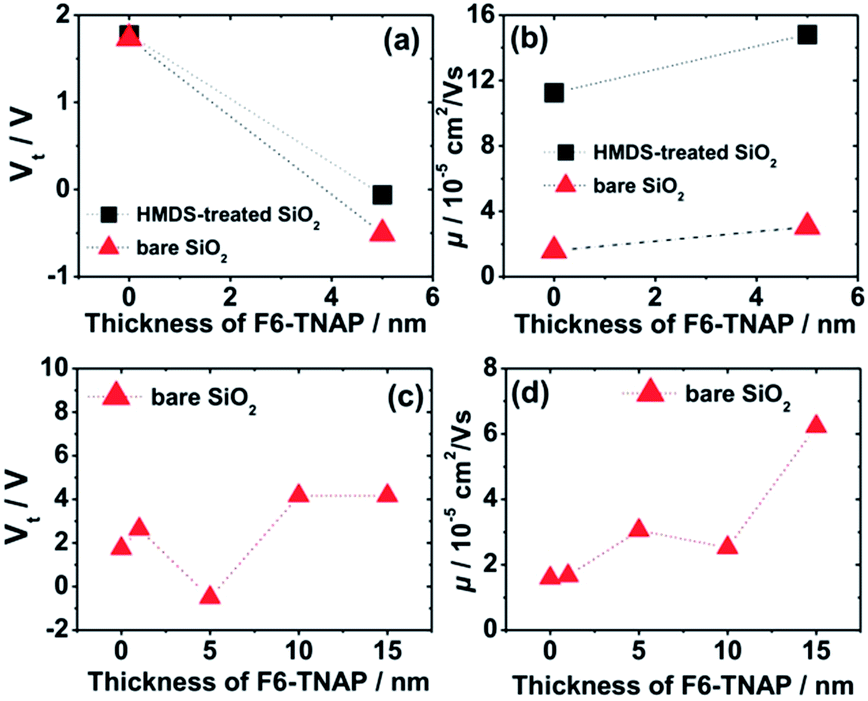 | ||
| Fig. 4 (a) The fitted threshold voltage Vt and (b) hole mobility μ of F6-TNAP/Spiro-TAD field-effect transistors fabricated on bare SiO2 and HMDS-treated SiO2. (c) Vt and (d) μ of F6-TNAP/Spiro-TAD devices fabricated on bare SiO2 with different thicknesses of F6-TNAP. | ||
There is also a difference in Vt of 0.4 V for devices without and with a 5 nm thick F6-TNAP interlayer. Therefore, the gate dielectric treatment and additional layer of F6-TNAP slightly influence the fitted threshold voltage or the switch-on voltage of the corresponding devices. Also, the hole mobility in devices utilizing bare SiO2 is lower by a factor of 7 than that in devices utilizing HMDS-treated SiO2, as displayed in Fig. 4b. An additional layer of 5 nm thick F6-TNAP sandwiched between SiO2 and Spiro-TAD results in higher hole mobility for both devices, but the difference in the fitted threshold voltages is less than 1 V.
Due to higher MR obtained for devices fabricated on bare SiO2, we subsequently investigated the influence of F6-TNAP thickness on the threshold voltage and hole mobility in the saturation region (Fig. 4c and d). In this case the mobility of holes slightly increases with increasing thickness of F6-TNAP and the fitted threshold voltage increases as well toward positive values. The corresponding MR values for devices fabricated with different thicknesses of F6-TNAP interlayer (1 nm, 5 nm, 10 nm and 15 nm) while the thickness of Spiro-TAD was kept constant at 40 nm are depicted in Fig. 5, showing high reproducibility of the results. We achieved MR values of ∼0.1% for all devices with F6-TNAP thicknesses of 1 nm and 10 nm. On the other hand, MR values of ∼0.05% were obtained for devices with F6-TNAP thicknesses of 5 nm and 15 nm. In this case we cannot see a direct correlation between the thickness of F6-TNAP and MR values.
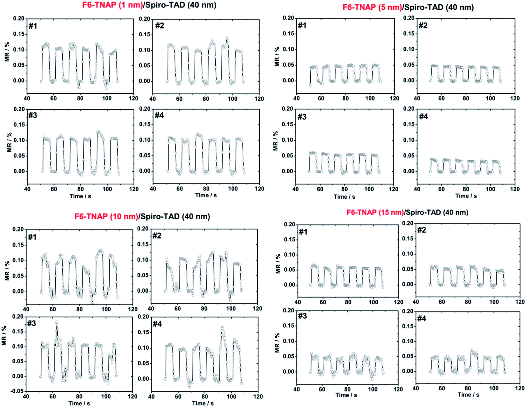 | ||
| Fig. 5 The experimental data of MR effects obtained by switching a constant magnetic field on and off six times in a row, showing the reproducibility of MR in field-effect transistors based on F6-TNAP (x nm)/Spiro-TAD (40 nm) bilayer. Here, x is 1, 5, 10 and 15 nm. For each thickness of F6-TNAP the data for four identical devices are shown, which are labeled as #1, #2, #3 and #4. All devices have channel length and width of 20 μm and 10 mm, respectively. All MR values displayed here are recorded at Vg = Vd = −40 V. | ||
MR values were also measured and calculated at different Vd and Vg, including the details of magnetic field dependency behaviors. Fig. 6a shows the dependency of MR values on both Vd and Vg. In this case, only positive MR values are obtained and no sign change of MR is observed in the range of our applied voltages. However, the MR values depend on the Vd and Vg and the highest MR value is achieved at high |Vg| and low |Vd|. Fig. 6b shows the magnetic field dependency measurements at a constant Vd of −20 V and at Vg of −10 V, −40 V and −80 V. A significant increase in MR with increasing |Vg| is obtained at constant |Vd|. In contrast, at constant |Vg| a decrease in MR is observed with increasing |Vd|, as displayed in Fig. 6c. The data shown in Fig. 6b and c are consistent with the results shown in Fig. 6a. Furthermore, the magnetic field dependency curves were fitted by using empirical laws: non-Lorentzian MR ∼ B2/(B + B0)2 and Lorentzian MR ∼ B2/(B2 + B02), where B0 is a constant. Both functions fitted our data very well with coefficient of correlation higher than 0.98. The fitting with non-Lorentzian line shape gave relatively small values of B0 between 3.9 ± 0.2 mT and 5.2 ± 0.3 mT, which are comparable to those obtained for other organic semiconductors.10 In contrast, the fitting with Lorentzian function gave values of the constant B0 of between 8.1 ± 0.4 mT and 10.2 ± 0.5 mT, which are much larger than those obtained with non-Lorentzian line shape.
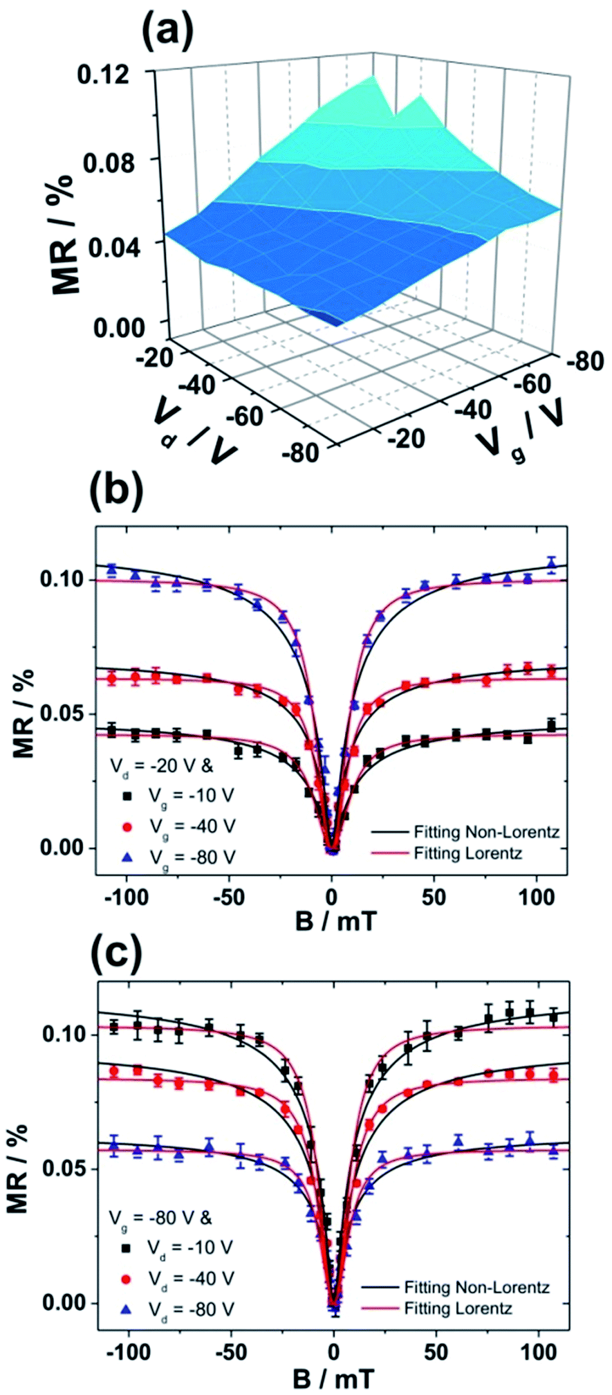 | ||
| Fig. 6 (a) A “landscape” of MR values measured at different Vd and Vg for bilayer thin films of F6-TNAP (5 nm)/Spiro-TAD (40 nm) field-effect transistor fabricated on bare SiO2. Magnetic field dependence of MR measured at (b) constant Vd for different Vg and at (c) constant Vg for different Vd. The corresponding data were plotted by using non empirical laws of non-Lorentzian and Lorentzian line shapes. | ||
2.3. Discussion about the origin of MR
Now we attempt to explain the general underlying physical mechanism of the MR effect observed in our unipolar p-channel Spiro-TAD field-effect transistor measured at low fields of <100 mT and room temperature, including the role of F6-TNAP sandwiched between SiO2 and Spiro-TAD. Firstly, we compare the performance of pristine Spiro-TAD devices fabricated on bare SiO2 and HMDS-treated SiO2. Spiro-TAD itself is a p-type organic semiconductor that does not transport electrons in a field-effect transistor.30,32 A bare SiO2 surface contains high concentrations of natural defects, free radicals, OH groups, peroxide bridges and non-bridging oxygen centers.36 These defects are expected to lead to dipole moments of the order of a few debyes that give rise to transport traps for carriers in the nearby channel of the field-effect transistor.37,38 Therefore, in the conducting channel we have mobile positive charges (holes) originated from the hole injection into the Spiro-TAD and fixed immobile electron or acceptor-like traps, indicated by positive fitted threshold voltage.39 In contrast, a HMDS-treated SiO2 surface contains qualitatively lower density of traps with respect to a pristine SiO2 surface. This implies that quasi particles participating in the transport process and MR effect are holes and immobile electron or acceptor-like traps. For this reason the excitonic and triplet exciton–polaron interaction models can be excluded for explaining MR effects in Spiro-TAD transistors. One possible model for explaining our result is the bipolaron model, which is also the most suitable model for unipolar devices.21,40The main differences between transistors fabricated on bare SiO2 and on HMDS-treated SiO2 are in terms of density of traps, current density of the corresponding transistors and interface characteristics between SiO2 and Spiro-TAD. The device fabricated on bare SiO2 has lower current density, but higher density of traps. In contrast, the device fabricated on HMDS-treated SiO2 has higher current density, but lower density of traps. Despite its high current density a negligible MR is obtained for the device utilizing HMDS-treated SiO2, which is in contrast to the device fabricated on bare SiO2. For explaining our results we propose two possible mechanisms, which are relevant to each other: (i) trapped charge-stabilized bipolaron intermediate states and (ii) broadening density of states and its correlation to bipolaron formation.
Firstly, there is a hint obtained from the experiments that the MR effect is strongly affected by electron traps. Therefore, we suggest the stabilization of bipolaron species by electron traps as a possible occurrence. In Spiro-TAD transistors holes are injected and transported via a hopping process through a limited number of percolation paths. Thus, one hole may block the transport of other holes. During the transport process a bipolaron consisting of two identical charge carriers can be formed as an intermediate state for which the spin configuration of bipolaron species is influenced by an external magnetic field, especially for fields larger than the random hyperfine fields. At zero fields a large current is obtained caused by the spin mixing between singlet and triplet states. In contrast, a lower current is achieved at fields larger than the random hyperfine fields because the spin mixing between singlet and triplet is lifted up. As a result, positive MR is expected to be obtained in the bipolaron model. However, due to its high on site exchange energy the bipolaron species is not stable and is only available as an intermediate state. One possible way to stabilize the bipolaron species is via an interaction with opposite trapped charge. Therefore, higher MR values are obtained for devices fabricated on bare SiO2 due to higher density of traps compared to the devices fabricated on HMDS-treated SiO2. The trapped charge-stabilized bipolaron species proposed in this work is quite similar to trion species.22,41
Secondly, the interface between bare SiO2 or HMDS-treated SiO2 and Spiro-TAD may play an important role as well. It has been suggested that the gate dielectric may induce broadening of the density of states (DOS) of an organic semiconductor by dipolar disorder at the interface.42,43 Therefore, low density of trapped charges at the SiO2 interface, which is more pronounced for devices fabricated on bare SiO2, slightly broadens the DOS.44 As a result, a slightly larger energetic disorder can be expected for devices fabricated on bare SiO2, which is beneficial for compensating the energy cost for bipolaron formation. This in turn gives rise to relatively higher bipolaron formation rate and, hence, it gives higher MR values for Spiro-TAD transistors fabricated on bare SiO2. We also conjecture the synergy between the first and the second mechanism as an origin of the MR effect in unipolar Spiro-TAD field-effect transistors.
The second important result obtained in our experiment is the influence of organic molecular p-dopant F6-TNAP on the MR effects. A significant increase in MR values was obtained when an additional thin layer of F6-TNAP was deposited between SiO2 and Spiro-TAD. For specifying the origin of this effect we measured the absorption spectra of the corresponding films, as shown in Fig. 7. In this case the UV-Vis-NIR absorption spectra were recorded for pristine Spiro-TAD and bilayer films of Spiro-TAD with different thicknesses of F6-TNAP. For bilayer films two new absorption bands were obtained at 450 nm and 825 nm, respectively. The absorption maximum at 450 nm can be assigned to the fingerprint of radical cation Spiro-TAD˙+, which is in agreement with the absorption of radical cation Spiro-TAD˙+ measured in dichloromethane by means of a spectroelectrochemical method (see Fig. S7†). The NIR absorption occurring at 825 nm can be attributed to the radical anion F6-TNAP˙− (see Fig. S8†).33 These results imply an interfacial doping of Spiro-TAD with F6-TNAP.33,45 As a result, the hole density in the transistor channel is expected to increase upon doping with F6-TNAP as indicated by higher drain current, as displayed in Fig. 3a. The mechanism for charge transfer could originate via two different ways that could not be distinguished in our case, namely integer charge transfer and hybrid charge transfer.46,47 Recently, the use of F6-TNAP as p-dopant has been demonstrated for doping N,N,N′,N′-tetrakis(4-methoxyphenyl)benzidine (MeO-TPD)48 or N,N′-di-1-naphthyl-N,N′-diphenyl-1,1′-biphenyl-4,4′-diamine (α-NPD)33 and pentacene.49
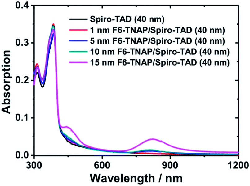 | ||
| Fig. 7 UV-Vis-NIR absorption spectra of pristine Spiro-TAD and F6-TNAP and Spiro-TAD bilayer thin films deposited on a glass substrate. | ||
Based on our experiment we conclude that an increase in MR in devices containing F6-TNAP strongly corresponds to the interfacial doping of Spiro-TAD with that compound. On the one hand, the doping process increases the net of charge carriers and, therefore, leads to a better conductivity. On the other hand, the doping process creates more traps, which reduce the charge carrier hopping rate.50 Thus, the overall number of electron traps is higher for devices fabricated with F6-TNAP, making the stabilization of bipolaron intermediate state more effective and resulting in higher MR values with respect to pristine Spiro-TAD. Also, broader density of states is also assumed to be obtained upon doping F6-TNAP into Spiro-TAD, enlarging the energetic disorder compared to pristine Spiro-TAD. As a consequence, the bipolaron formation rate is increased for doping systems due to higher energetic disorder of those systems. This argument is supported by an experiment which reported the density of states in undoped and doped amorphous organic films of α-NPD with tetrafluorocyanoquinodimethane (F4-TCNQ).51
The effect of doping on the DOS has been analytically studied, showing an increase in the DOS and broadening the deep tail of the DOS distribution due to the interaction between dopant ions and localized carriers.50 In our argument we consider a slow-hopping process in which the spin mixing should be completed before a specific pair is formed or dissociated. In other words, the average hopping rate is much smaller than the precession frequency of spins at specific molecular sites.21,40 However, the hole mobility extracted from the transfer curves was found to be constant or not affected significantly by external magnetic fields (see Fig. S9†), which is in contrast to the bipolaron model that suggests a change in mobility is expected under the influence of external magnetic fields. In our study, such a change in mobility has not been observed and obtained and this is probably due to only a small number of charge carriers participating in bipolaron formation (due to three-dimensional hopping transports) with respect to the total drain current. Therefore, a change in current caused by external magnetic fields is too small to be detected and measured.
Now we have to consider the influence of electric fields (mainly lateral field due to Vd). If sufficient electric field is available to dissociate the CT state, we will have extra positive charges (secondary charges) that participate in the conducting channel, and extra negative charges, acting as traps. The CT state itself can have larger binding energies, but the lateral electric field Vd can (partially) overcome the corresponding binding energies. Hence, the dissociation probability of the 1CT state increases with increasing lateral electric field.52 The dependency of MR on Vg and Vd is shown in Fig. 6a for which the gate field Eg (Eg = |Vg|/d, where d is the thickness of SiO2) is much larger than the drain field Ed (Ed = |Vd|/L, where L is the channel length). In this case, the gate-induced charge in the conducting channel increases by increasing |Vg| at a given |Vd|. On the other hand, at a given |Vg|, increasing |Vd| will increase the number of charge carriers flowing between source and drain electrodes.
For the sake of simplicity, at constant |Vd| we have a constant dissociation rate and, therefore, MR increases with increasing |Vg| due to more induced charge carriers being available in the channel that participate in bipolaron formation, as displayed in Fig. 6b. The situation changes significantly when |Vg| is kept constant, which means the number of gate-induced charges is constant. Then, increasing |Vd| will decrease MR values, as shown in Fig. 6c. This can be explained by using electric field enhanced dissociation rate. At low |Vd| (and at high constant |Vg|) the dissociation rate of 1CT is low and, thus, the subtracted secondary charges and traps are low as well. However, the overall density of charges and traps is higher than devices without F6-TNAP. Therefore, higher MR values are obtained due to higher density of trapped charge-stabilized bipolaron species. High |Vd| value increases the dissociation rate of 1CT and, therefore, the numbers of secondary charges and traps increase as well. However, we conjecture that at high |Vd| the charge carrier has relatively high drift velocity. As a consequence, the hopping rate is probably higher, shortening the interaction time between quasi particles and hampering the formation of bipolaron species. As a result, at high |Vd| fewer bipolaron species are available in the conducting channel, decreasing the density of trapped charge-stabilized bipolaron species and decreasing the overall MR at high |Vd| as well. This argument is supported by Fig. 6, which shows that at a given |Vg| the MR values decrease with increasing |Vd|.
It is also worth noting that the competition between electrical drifting force and local Coulomb interaction determines the formation and dissociation probabilities of electron–hole pairs in the CT states.53 Also, the donor and acceptor interaction is determined by the intermolecular distance and the electronegativity difference between the donor and acceptor molecules.54 The overall MR values reported in this work are quite low, but significant. Such low MR values can be attributed to the three-dimensional hopping conduction in thin films of amorphous Spiro-TAD field-effect transistors because only a small number of bipolaron species participates in MR effects. Recently, a giant MR effect has been reported for molecular wires for which the spin blockade is dominated in one-dimensional hopping transport.55
3. Conclusions
In conclusion, we show the MR effect in a unipolar p-channel field-effect transistor based on amorphous thin films of Spiro-TAD. MR values obtained for pristine Spiro-TAD devices fabricated on bare SiO2 gate dielectric are higher than those for devices fabricated on HMDS-treated SiO2. An additional thin layer of organic molecular p-dopant F6-TNAP sandwiched between SiO2 and Spiro-TAD further increases the overall MR values with respect to devices fabricated without F6-TNAP.We propose two possible explanations for MR effects in Spiro-TAD field-effect transistors. Firstly, a trapped charge-stabilized bipolaron species is suggested. In this case, higher MR is obtained for devices containing larger amounts of electron traps. Secondly, the interface between bare SiO2 or HMDS-treated SiO2 and Spiro-TAD modifies the density of states due to the different dipolar disorder at the corresponding interface. As a consequence, a different energetic disorder is achieved, which is larger for devices fabricated on bare SiO2 caused by higher density of traps. This physical characteristic is beneficial for compensating the energy cost for bipolaron formation. Thus, more bipolaron species are formed during the transport process and participate in magnetic field effects, increasing the overall MR values. The MR values increase for devices with an additional layer of organic molecular p-dopant F6-TNAP due to an increase in charge carriers and traps.
4. Experimental section
Bottom-contact field-effect transistor substrates were purchased from Fraunhofer IPMS (Dresden, Germany). We used a channel length (L) of 20 μm and a channel width (W) of 10 mm. The gate dielectric consisted of 230 ± 10 nm thick SiO2 and the source and drain electrodes were 30 nm Au with 10 nm ITO as adhesion layer. Prior to the deposition of organic materials the predefined substrates were cleaned with acetone and 2-propanol, followed by oxygen-plasma treatment. This gate dielectric is denoted as “bare SiO2”. Then, the gate dielectric SiO2 was exposed to HMDS (under vacuum, 130 °C, for 20 minutes), which is called “HMDS-treated SiO2”. Finally, Spiro-TAD and F6-TNAP were deposited by thermal evaporation process at a base pressure of 1 × 10⁻⁷ Torr (Tsubstrate = 298 K) with a thickness between 0 and 15 nm for F6-TNAP and a thickness of 40 nm for Spiro-TAD. Spiro-TAD was synthesized and purified in our laboratory. F6-TNAP (LT-N223) was purchased from Lumtec (Taiwan) and was used as received. From the vacuum chamber the samples were directly transferred to a glove box (O2, H2O < 0.1 ppm) and placed in a homebuilt sample holder. This sample holder was placed between the poles of an (unshielded) electromagnet. The magnetic field was varied between −100 mT and +100 mT. The data acquisition process and the calculation of MR values have been described in detail elsewhere.28,29 The hole mobility and the threshold voltage have been calculated at the saturation regime.30 Current–voltage measurements were performed using a Keithley 4200 semiconductor characterization system equipped with preamplifiers for improving low-current measurements. All measurements were performed at room temperature. All magnetic field-effect experiments were carried out at a magnetic field of 96 mT, except for magnetic field dependence measurements.The UV-Vis-NIR spectra of thin films were recorded with a Perkin-Elmer Lambda 900 UV-Vis-NIR spectrophotometer. The cyclic voltammetry (CV) measurements were carried out with an EG & G Princeton Applied Research model 273 A potentiostat/galvanostat in a three-electrode, single-compartment cell equipped with a platinum disc working electrode, a glassy carbon counter electrode and an Ag/AgCl reference electrode. The CV measurements were carried out in dichloromethane containing 0.1 M tetrabutylammonium hexafluorophosphate (TBAHFP) as a supporting electrolyte. Solutions were purged with nitrogen prior to conducting the experiments. All measurements were performed under nitrogen atmosphere at room temperature with a scan rate of 50 mV s−1 and were referenced against ferrocene/ferrocenium (Fc/Fc+) as internal standard reference. In situ UV-Vis-NIR spectroelectrochemical measurement of Spiro-TAD was carried out in MeCN/0.1 M TBAHFP at room temperature. The spectroelectrochemical experiment was carried out with the same equipment as for the CV experiment and is described in detail elsewhere.56,57
Acknowledgements
We acknowledge T. Reichert for intensive discussion about this theme and providing us the analysis of magnetic field dependence measurements and J. Salbeck for his long-standing support in this new research area. We also thank A. Scheffler for providing us with the electrochemistry data of compounds used in this experiment.Notes and references
- C. K. Chiang, C. R. Fincher Jr, Y. W. Park, A. J. Heeger, H. Shirakawa, E. J. Louis, S. C. Gau and A. G. MacDiarmid, Phys. Rev. Lett., 1977, 39, 1098 CrossRef CAS.
- S. Reineke, F. Lindner, G. Schwartz, N. Seidler, K. Walzer, B. Lüssem and K. Leo, Nature, 2009, 459, 234 CrossRef CAS PubMed.
- Heliatek GmbH, Neuer Weltrekord für organische Solarzellen: Heliatek behauptet sich mit 12% Zelleffizienz als Technologieführer, http://www.heliatek.com, January, 2013.
- H. Minemawari, T. Yamada, H. Matsui, J. Tsutsumi, S. Haas, R. Chiba, R. Kumai and T. Hasegawa, Nature, 2011, 475, 364 CrossRef CAS PubMed.
- I. Zutic, J. Fabian and S. Das Sarma, Rev. Mod. Phys., 2004, 76, 323 CrossRef CAS.
- Z. H. Xiong, D. Wu, Z. V. Vardeny and J. Shi, Nature, 2004, 427, 821 CrossRef CAS PubMed.
- D. Sun, L. Yin, C. Sun, H. Guo, Z. Gai, X. G. Zhang, T. Z. Ward, Z. Cheng and J. Shen, Phys. Rev. Lett., 2010, 104, 236602 CrossRef.
- X. Zhang, S. Mizukami, T. Kubota, Q. Ma, M. Oogane, H. Naganuma, Y. Ando and T. Miyazaki, Nat. Commun., 2013, 4, 1392 CrossRef PubMed.
- T. D. Nguyen, E. Ehrenfreund and Z. V. Vardeny, Science, 2012, 337, 204 CrossRef CAS PubMed.
- Ö. Mermer, G. Veeraraghavan, T. L. Francis, Y. Sheng, D. T. Nguyen, M. Wohlgenannt, A. Köhler, M. K. Al-Suti and M. S. Khan, Phys. Rev. B: Condens. Matter Mater. Phys., 2005, 72, 205202 CrossRef.
- T. D. Nguyen, Y. Sheng, J. Rybicki and M. Wohlgenannt, Phys. Rev. B: Condens. Matter Mater. Phys., 2008, 77, 235209 CrossRef.
- H. Gu, J. Guo, Q. He, Y. Jiang, Y. Huang, N. Haldolaarachige, Z. Luo, D. P. Young, S. Wei and Z. Guo, Nanoscale, 2014, 6, 181 RSC.
- J. Guo, H. Gu, H. Wei, Q. Zhang, N. Haldolaarachige, Y. Li, D. P. Young, S. Wie and Z. Guo, J. Phys. Chem. C, 2013, 117, 10191 CAS.
- H. Gu, J. Guo, X. Zhang, Q. He, Y. Huang, H. A. Colorado, N. Haldolaarachige, H. Xin, D. P. Young, S. Wei and Z. Guo, J. Phys. Chem. C, 2013, 117, 6426 CAS.
- H. Gu, H. Wie, J. Guo, N. Haldolaarachige, D. P. Young, S. Wie and Z. Guo, Polymer, 2013, 54, 5974 CrossRef CAS PubMed.
- H. Gu, J. Guo, H. Wei, Y. Huang, C. Zhao, Y. Li, Q. Wu, N. Haldolaarachige, D. P. Young, S. Wie and Z. Guo, Phys. Chem. Chem. Phys., 2013, 15, 10866 RSC.
- H. Gu, X. Zhang, H. Wie, Y. Huang, S. Wie and Z. Guo, Chem. Soc. Rev., 2013, 42, 5907 RSC.
- B. Hu, L. Yan and M. Shao, Adv. Mater., 2009, 21, 1500 CrossRef CAS PubMed.
- V. Prigodin, J. Bergeson, D. Lincoln and A. Epstein, Synth. Met., 2006, 156, 757 CrossRef CAS PubMed.
- P. Desai, P. Shakya, T. Kreouzis, W. P. Gillin, N. A. Morpley and M. R. J. Gibbs, Phys. Rev. B: Condens. Matter Mater. Phys., 2007, 75, 094423 CrossRef.
- P. A. Bobbert, T. D. Nguyen, F. W. A. van Oost, B. Koopmans and M. Wohlgenannt, Phys. Rev. Lett., 2007, 99, 216801 CrossRef CAS.
- M. Cox, P. Janssen, F. Zhu and B. Koopmans, Phys. Rev. B: Condens. Matter Mater. Phys., 2013, 88, 035202 CrossRef.
- C. Boehme and J. M. Lupton, Nat. Nanotechnol., 2013, 8, 612 CrossRef CAS PubMed.
- M. Nishioka, Y. B. Lee, A. M. Goldman, Y. Xia and C. D. Frisbie, Appl. Phys. Lett., 2007, 91, 092117 CrossRef PubMed.
- T. P. I. Saragi and T. Reichert, Appl. Phys. Lett., 2012, 100, 073304 CrossRef PubMed.
- T. Reichert and T. P. I. Saragi, Appl. Phys. Lett., 2011, 98, 063307 CrossRef PubMed.
- T. Reichert and T. P. I. Saragi, Org. Electron., 2012, 13, 377 CrossRef CAS PubMed.
- T. Reichert, T. P. I. Saragi and J. Salbeck, RSC Adv., 2012, 2, 7388 RSC.
- E. Tatarov, T. Reichert, T. P. I. Saragi, A. Scheffler, R. Ueberschaer, C. Bruhn, T. Fuhrmann-Lieker and J. Salbeck, Chem. Commun., 2013, 49, 4564 RSC.
- T. P. I. Saragi, T. Fuhrmann-Lieker and J. Salbeck, Adv. Funct. Mater., 2006, 16, 966 CrossRef CAS PubMed.
- T. P. I. Saragi, T. Spehr, A. Siebert, T. Fuhrmann-Lieker and J. Salbeck, Chem. Rev., 2007, 107, 1011 CrossRef CAS PubMed.
- T. P. I. Saragi, T. Fuhrmann-Lieker and J. Salbeck, Synth. Met., 2005, 148, 256 CrossRef PubMed.
- P. K. Koech, A. B. Padmaperuma, L. Wang, J. S. Swensen, E. Polikarpov, J. T. Darsell, J. E. Rainbolt and D. J. Gaspar, Chem. Mater., 2010, 22, 3926 CrossRef CAS.
- M. Thomschke, PhD Thesis, Technische Universität Dresden, September, 2012.
- H. B. Michaelson, J. Appl. Phys., 1977, 48, 4729 CrossRef CAS PubMed.
- S. J. Konezny, M. N. Bussac and L. Zuppiroli, Phys. Rev. B: Condens. Matter Mater. Phys., 2010, 81, 045313 CrossRef.
- J. W. Raymonda, J. S. Muenter and W. A. Klemperer, J. Chem. Phys., 1970, 52, 3458 CrossRef CAS PubMed.
- R. W. Fessenden, A. Hitachi and V. Nagarajan, J. Phys. Chem., 1984, 88, 107 CrossRef CAS.
- (a) S. G. J. Mathijssen, M. J. Spijkman, A. M. Andringa, P. A. van Hal, I. McCulloch, M. Kemerink, R. A. J. Janssen and D. M. de Leeuw, Adv. Mater., 2010, 22, 5105 CrossRef CAS PubMed; (b) S. Scheinert, K. P. Perntich, B. Batlogg and G. Paasch, J. Appl. Phys., 2007, 102, 104503 CrossRef PubMed; (c) L. L. Chua, J. Zaumseil, J. F. Chang, E. C. W. Ou, P. K. H. Ho, H. Sirringhaus and R. H. Friend, Nature, 2005, 434, 194 CrossRef CAS PubMed.
- W. Wagemans, P. Janssen, A. J. Schellekens, F. L. Bloom, P. A. Bobbert and B. Koopmans, Spin, 2011, 1, 93 CrossRef CAS.
- A. Kadashchuk, V. I. Arkhipov, C. H. Kim, J. Shinar, D. W. Lee, Y. R. Hong, J. I. Jin, P. Heremans and H. Bässler, Phys. Rev. B: Condens. Matter Mater. Phys., 2007, 76, 235205 CrossRef.
- J. Veres, S. D. Ogier, S. W. Leeming, D. C. Cupertino and S. M. Khaffaf, Adv. Funct. Mater., 2003, 13, 199 CrossRef CAS PubMed.
- H. Sirringhaus, Adv. Mater., 2009, 21, 3859 CrossRef CAS PubMed.
- N. Tessler, Y. Preezant, N. Rappaport and Y. Roichman, Adv. Mater., 2009, 21, 2741 CrossRef CAS PubMed.
- B. Lüssem, M. Riede and K. Leo, Phys. Status Solidi A, 2013, 210, 9 CrossRef PubMed.
- S. Braun, W. R. Salaneck and M. Fahlman, Adv. Mater., 2009, 21, 1 CrossRef PubMed.
- I. Salzmann, G. Heimel, S. Duhm, M. Oehzelt, P. Pingel, B. M. George, A. Schnegg, K. Lips, R. P. Blum, A. Vollmer and N. Koch, Phys. Rev. Lett., 2012, 108, 035502 CrossRef.
- J. H. Lee, J. Lee, Y. H. Kim, C. Yun, B. Lüssem and K. Leo, Org. Electron., 2014, 15, 16 CrossRef CAS PubMed.
- B. Lüssem, M. L. Tietze, H. Kleemann, C. Hoßbach, J. W. Bartha, A. Zakhidov and K. Leo, Nat. Commun., 2013, 4, 2775 Search PubMed.
- V. I. Arkhipov, P. Heremans, E. V. Emelianova and H. Bässler, Phys. Rev. B: Condens. Matter Mater. Phys., 2005, 71, 045214 CrossRef.
- O. Tal, Y. Rosenwaks, Y. Preezant, N. Tessler, C. K. Chan and A. Kahn, Phys. Rev. Lett., 2005, 95, 256405 CrossRef CAS.
- C. L. Braun, J. Chem. Phys., 1984, 80, 4157 CrossRef CAS PubMed.
- H. Zang, Z. Xu and B. Hu, J. Phys. Chem. B, 2010, 114, 5704 CrossRef CAS PubMed.
- Z. Xu and B. Hu, Adv. Funct. Mater., 2008, 18, 2611 CrossRef CAS PubMed.
- R. N. Mahato, H. Lülf, M. H. Siekman, S. P. Kersten, P. A. Bobbert, M. P. de Jong, L. De Cola and W. G. van der Wiel, Science, 2013, 341, 257 CrossRef CAS PubMed.
- J. Salbeck, Anal. Chem., 1993, 65, 2169 CrossRef CAS.
- A. Scheffler, PhD Thesis, University of Kassel, November, 2011.
Footnote |
| † Electronic supplementary information (ESI) available: Output and transfer curves, magnetoresistance measurements, UV-Vis spectroscopy and electrochemistry. See DOI: 10.1039/c4tc00702f |
| This journal is © The Royal Society of Chemistry 2014 |