 Open Access Article
Creative Commons Attribution 3.0 Unported Licence
Geometry of tellurene adsorbed on the Si(111)- R30°-Sb surface from first principles calculations†
Stefania
Isceri‡
 ab,
Daniele
Dragoni§
 c,
Davide
Campi
 c,
Stefano
Cecchi
 bc and
Marco
Bernasconi
 *c
*c
aDepartment of Physics, Politecnico di Milano, Piazza L. da Vinci 32, 20133, Milano, Italy
bPaul-Drude-Institut für Festkörperelektronik, Leibniz-Institut im Forschungsverbund Berlin e. V., Hausvogteiplatz 5-7, 10117, Berlin, Germany
cDepartment of Materials Science, University of Milano-Bicocca, Via R. Cozzi 55, 20125, Milano, Italy. E-mail: marco.bernasconi@unimib.it
First published on 27th July 2022
Abstract
The 2D form of tellurium, named tellurene, is one of the latest discoveries in the family of 2D mono-elemental materials. In a trilayer configuration, free-standing tellurene was predicted theoretically to acquire two crystallographic forms, the α and β phases, corresponding to either a 1T-MoS2-like geometry or a trilayer slab exposing the Te(10![[1 with combining macron]](https://www.rsc.org/images/entities/char_0031_0304.gif) 0) surface of bulk Te with helical chains lying in-plane and further reconstructed due to the formation of interchain bonds. Either one or the other of the two phases was observed experimentally to prevail depending on the substrate they were grown onto. In the perspective to integrate tellurene on silicon, we here report an ab initio study of the adsorption of tellurene on the Si(111)-
0) surface of bulk Te with helical chains lying in-plane and further reconstructed due to the formation of interchain bonds. Either one or the other of the two phases was observed experimentally to prevail depending on the substrate they were grown onto. In the perspective to integrate tellurene on silicon, we here report an ab initio study of the adsorption of tellurene on the Si(111)- R30° surface passivated by antinomy. According to the literature, this substrate is chosen for the growth of several tellurides by molecular beam epitaxy. The calculations reveal that on this substrate the adsorption energy mostly compensates the energy difference between the α and β phases in the free-standing configuration which suggests that the prevalence of one phase over the other might in this case strongly depend on the kinetics effects and deposition conditions.
1 Introduction
Mono-elemental 2D materials referred to as Xenes, where X is an element of the groups III, IV, V or VI, have attracted great interest in recent years because of their extraordinary mechanical, electrical, and optical properties, which are different from those of their counterparts in the bulk phase.1The two-dimensional form of tellurium, known as tellurene, is one of the latest found materials in this class.1 In the bulk under normal conditions, tellurium crystallizes in a trigonal phase (space group P3121)2 made of helical chains with short (2.835 Å) Te–Te intrachain bonds. Weak interchain interactions lead to a hexagonal arrangement of the chains aligned along the c axis (in the hexagonal setting of the trigonal phase with a = 4.45 Å and c = 5.93 Å). Due to its quasi-one-dimensional character, Te is less prone to be exfoliated into 2D sheets, although examples of mechanical exfoliation have been reported in the literature.3 Most often 2D tellurium is grown in the form of flakes in solution4 or is deposited as ultrathin films on different substrates by several means. For instance, molecular beam epitaxy (MBE) on graphene supported by a 6H-SiC(0001) substrate leads to the formation of helical chains with their axis lying parallel to the substrate which corresponds to the formation of the Te(10![[1 with combining macron]](https://www.rsc.org/images/entities/char_0031_0304.gif) 0) face of bulk tellurium.5 This is actually the truncation of the bulk with the lowest surface energy.6 No preferred orientation between the Te chains and the substrate is observed because of the van der Waals epitaxy.5 The band gap of the films increases by decreasing the thickness from 0.33 eV (bulk) to 0.92 eV (a single chain layer) as measured by scanning tunneling microscopy.5 A field-effect transistor made of flakes of tellurene grown in solution in the Te(10
0) face of bulk tellurium.5 This is actually the truncation of the bulk with the lowest surface energy.6 No preferred orientation between the Te chains and the substrate is observed because of the van der Waals epitaxy.5 The band gap of the films increases by decreasing the thickness from 0.33 eV (bulk) to 0.92 eV (a single chain layer) as measured by scanning tunneling microscopy.5 A field-effect transistor made of flakes of tellurene grown in solution in the Te(10![[1 with combining macron]](https://www.rsc.org/images/entities/char_0031_0304.gif) 0) geometry was actually reported in the literature with hole mobilities as high as about 700 cm2 V−1 s−1 at 300 K.4
0) geometry was actually reported in the literature with hole mobilities as high as about 700 cm2 V−1 s−1 at 300 K.4
The growth of helical chains with their axis perpendicular to that of the substrate has been attained instead by Wang et al.7 on flexible mica sheets with a film thickness of 32 nm. This geometry corresponds to the exposure of the (0001) surface of bulk Te.
On the other hand, theoretical calculations based on density functional theory (DFT) have shown that a free-standing trilayer made of helical chains lying in-plane is unstable with respect to a reconstruction forming additional interchain bonds.8 This geometry is referred to as the β phase in ref. 8 and it is consistent with the structure of ultrathin films grown on highly oriented pyrolytic graphite (HOPG).8,9
Moreover, a trilayer corresponding to the truncation of the helical chains growing perpendicular to the layer plane exposing the Te(0001) face was shown to be unstable with respect to the formation of a trilayer 1T-MoS2-like geometry, called the α phase in ref. 8. The 1T-MoS2-like structure was later found to be consistent with transmission electron microscopy (TEM) images of ultrathin films grown by physical vapor deposition (PVD) on silica.10
The morphology and crystal structure of tellurene seem thus dependent on the growth method, the choice of the substrate and the film thickness.
The exploitation of tellurene in electronic devices, such the field-effect transistors already mentioned4 or photodetector devices,11 requires the development of large-area deposition of tellurene on a silicon substrate for eventual integration with standard microelectronic technologies. To this aim, a suitable passivation of the silicon surface is needed. Surface oxidation is a possible option which leads to an amorphous surface for the growth of 2D materials (see several examples in ref. 12). There are, however, numerous examples in the literature showing that the crystalline quality of epitaxial films of layered selenides can be improved by growing directly on the Si(111) surface with an adequate termination of the dangling bonds.13–15 Concerning tellurides, it has been shown that GeTe16 and layered Sb2Te3 and (GeTe)n (Sb2Te3)m17 can be grown in quasi single-crystalline films by MBE on the Si(111) surface passivated by Sb and reconstructed in a Si(111)- R30°-Sb geometry. In fact, this choice of the surface passivation mostly suppresses in-plane rotational domains, and for GeTe, it also reduces twinned domains, which are typical for chalcogenide thin films grown on Si(111).18,19 The reduction in the number of rotational domains is expected to reduce the overall number of defects leading to an improvement of the electrical mobility of the film which is beneficial for electronic and optoelectronic applications. The same Si(111) passivated substrate might thus be useful to grow ultrathin crystalline Te and tellurene films as well.
In this perspective, we here investigate the geometry of a trilayer of Te adsorbed on the Si(111)- R30°-Sb surface by DFT calculations. In particular, we compare the energetics of the formation of Te(10
![[1 with combining macron]](https://www.rsc.org/images/entities/char_0031_0304.gif) 0) termination, observed in ref. 5 on graphene, with the 1T-MoS2-like structure proposed in ref. 8.
0) termination, observed in ref. 5 on graphene, with the 1T-MoS2-like structure proposed in ref. 8.
2 Computational details
The geometry and adsorption energy of tullerene on the Si(111)- R30°-Sb surface were studied within the DFT framework implemented in the Quantum Espresso suite of programs.20,21 The exchange and correlation functional by Perdew, Burke and Ernzerhof (PBE)22 and norm-conserving pseudopotentials were employed. The Kohn–Sham (KS) orbitals were expanded on a plane wave basis set up to a kinetic energy cutoff of 24 Ry for geometry optimization at a fixed simulation cell. Optimization of the lattice parameters in a constant pressure relaxation algorithm was performed with a higher cutoff of 50 Ry for the convergence of the stress tensor. All energies reported hereafter refer to the calculation with 24 Ry. The semiempirical correction due to Grimme (D2)23 was added to include van der Waals (vdW) interactions. The Brillouin zone (BZ) integration was performed on Monkhorst-Pack meshes.24 The pseudopotential/PBE-D2 framework adopted here was also used and validated against different functionals for tellurene in ref. 8.
3 Results and discussion
In order to study the adsorption energy and geometry of tellurene on the Si surface, we first generated a slab model of silicon exposing the Si(111)- R30°-Sb surface on one side and a H-passivated 1 × 1 surface on the other side. We then optimized the geometry of pure Te in the bulk and of a free-standing trilayer of Te in a slab geometry either in the 1T-MoS2-like structure or exposing the Te(10
![[1 with combining macron]](https://www.rsc.org/images/entities/char_0031_0304.gif) 0) surface of the bulk.
0) surface of the bulk.
Although previous DFT calculations8 predicted that, in a free-standing trilayer, tellurene is most stable in the 1T-MoS2-like structure (α geometry of ref. 8), the interaction with the substrate might favor another configuration such as the Te(10![[1 with combining macron]](https://www.rsc.org/images/entities/char_0031_0304.gif) 0) geometry seen experimentally in ref. 5. We therefore considered both possibilities for the geometry of tellurene adsorbed on the Si(111)-
0) geometry seen experimentally in ref. 5. We therefore considered both possibilities for the geometry of tellurene adsorbed on the Si(111)- R30°-Sb surface.
The results of the individual steps summarized above are reported in the different subsections below.
3.1 The clean Si(111)- R30°-Sb surface
The theoretical lattice parameter and bulk modulus for bulk Si within our framework are 5.41 Å and 97 GPa which are close to the experimental values of 5.43 Å and 99 GPa.25 We used the theoretical equilibrium lattice parameter for bulk Si to optimize the model of the Si(111)- R30°-Sb surface in a slab with the bottom surface saturated by H in a 1 × 1 geometry. We applied 3D periodic boundary conditions with a vacuum 20 Å wide separating the periodic images along the direction perpendicular to the surface plane. The hexagonal surface unit cell has a lattice parameter of ahex equal to
  times the cubic lattice parameter of bulk Si which in our case yields ahex =
  × 5.407 Å = 6.622 Å.
The slab consists of four Si layers, a topmost Sb layer and a hydrogen bottom layer with three atoms per surface unit cell in each layer. The top and side views of the slab are shown in Fig. 1. According to the literature,26 the three Sb atoms per unit cell (one for each Si atom in the topmost surface layer) form a trimer whose center is aligned with the Si atom on the second layer in a site named T4.
We optimized the atomic positions in two steps: in the first step only the relaxation of hydrogen atoms was allowed in the c-direction, while all the other atoms were fixed at the ideal equilibrium sites of bulk Si. In the second step we relaxed all the atoms, apart from the hydrogen atoms and the Si atoms in the bottom layer which were kept fixed. Integration of the BZ was performed over a 5 × 5 × 1 MP mesh.
The final Si–H distance is 1.516 Å, whereas the interplanar distances between the n-th and the n-th + 1 Si layers (where n = 1 corresponds to the layer closest to the H atoms) are 0.692 Å, 2.297 Å and 0.896 Å. The distance between the top-most Si layer and the Sb layer is 2.557 Å.
3.2 Free-standing trilayer of tellurene
We first optimized a free-standing trilayer of tellurene in the 1T-MoS2-like structure shown in Fig. 2 which is the most stable configuration according to previous DFT calculations (α geometry of ref. 8). Integration of the BZ was performed over a 16 × 16 × 1 MP mesh. The equilibrium lattice parameters of the hexagonal surface unit cell (a) and the bond length (d) are a = 4.121 Å and d = 2.994 Å in good agreement with the DFT results of a = 4.15 Å and d = 3.02 Å in ref. 8.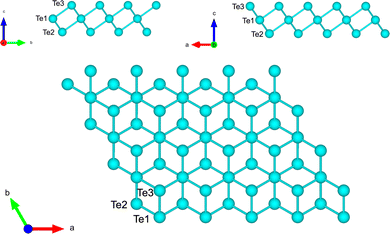 | ||
| Fig. 2 Side and top views of the optimized structure of tellurene in the 1T-MoS2-like geometry. The three atoms per unit cell are labelled. | ||
We then moved to a trilayer in a Te(10![[1 with combining macron]](https://www.rsc.org/images/entities/char_0031_0304.gif) 0) geometry.
0) geometry.
We first optimized the geometry of bulk trigonal Te which yielded the theoretical equilibrium lattice parameters of a = 4.318 Å and c = 5.934 Å to be compared with the experimental values27 of a = 4.45 Å and c = 5.93 Å.
Starting from the bulk geometry, we built a trilayer slab exposing the Te(10![[1 with combining macron]](https://www.rsc.org/images/entities/char_0031_0304.gif) 0) surface with helical chains lying in-plane as shown in Fig. 3. The unit cell is orthorhombic with the initial lattice parameters a and b corresponding to the a and c parameters of bulk Te (4.318 Å, b = 5.934 Å). Geometry optimization leads to a shrinking of the unit cell area with the formation of interchain bonds corresponding to the β geometry identified in ref. 8. The optimized lattice parameters of a = 4.142 Å and b = 5.449 Å are in good agreement with the previous DFT results of a = 4.17 Å and b = 5.49 Å in ref. 8. Integration of the BZ was performed over a 16 × 12 × 1 MP mesh.
0) surface with helical chains lying in-plane as shown in Fig. 3. The unit cell is orthorhombic with the initial lattice parameters a and b corresponding to the a and c parameters of bulk Te (4.318 Å, b = 5.934 Å). Geometry optimization leads to a shrinking of the unit cell area with the formation of interchain bonds corresponding to the β geometry identified in ref. 8. The optimized lattice parameters of a = 4.142 Å and b = 5.449 Å are in good agreement with the previous DFT results of a = 4.17 Å and b = 5.49 Å in ref. 8. Integration of the BZ was performed over a 16 × 12 × 1 MP mesh.
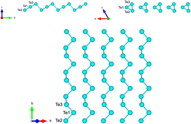 | ||
Fig. 3 Side and top views of the Te(10![[1 with combining macron]](https://www.rsc.org/images/entities/char_0031_0304.gif) 0) trilayer slab in the initial geometry obtained by truncation of the bulk. The three atoms per unit cell are labelled. 0) trilayer slab in the initial geometry obtained by truncation of the bulk. The three atoms per unit cell are labelled. | ||
The energy of the β phase is 68 meV per atom higher than the energy of the 1T-MoS2-like geometry in agreement with the value of 60 meV per atom reported in ref. 8.
By expanding the surface unit cell by about 7% with respect to the configuration of minimal energy of the β geometry, the helical chains are recovered as depicted in Fig. 4 which shows the energy vs the surface area of the Te(10![[1 with combining macron]](https://www.rsc.org/images/entities/char_0031_0304.gif) 0) trilayer slab. We remark that a previous DFT study,28 albeit with a functional different from ours, showed that the helical chains are stable in a double trilayer configuration with equilibrium lattice parameters of a = 4.36 Å and b = 5.81 Å the corresponding equilibrium area of which is shown as a dashed blue line in Fig. 4.
0) trilayer slab. We remark that a previous DFT study,28 albeit with a functional different from ours, showed that the helical chains are stable in a double trilayer configuration with equilibrium lattice parameters of a = 4.36 Å and b = 5.81 Å the corresponding equilibrium area of which is shown as a dashed blue line in Fig. 4.
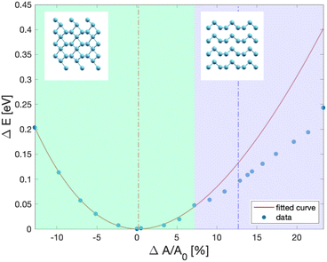 | ||
Fig. 4 Energy (dots) per unit cell (three atoms per cell) versus surface area of the Te(10![[1 with combining macron]](https://www.rsc.org/images/entities/char_0031_0304.gif) 0) trilayer slab from DFT calculations. The surface area is expressed in variation in % with respect to the area at the minimal energy (4.142 × 5.449 Å2, see text). The red line is a fitting of the data with a 2D version of the Birch–Murnaghan equation of state. In the green region the system is in the β geometry of ref. 8, while in the violet region the bulk-like helical chains are recovered. The insets show the crystal structure in the two regimes. The blue dashed line corresponds to the DFT equilibrium unit cell area of a Te(10 0) trilayer slab from DFT calculations. The surface area is expressed in variation in % with respect to the area at the minimal energy (4.142 × 5.449 Å2, see text). The red line is a fitting of the data with a 2D version of the Birch–Murnaghan equation of state. In the green region the system is in the β geometry of ref. 8, while in the violet region the bulk-like helical chains are recovered. The insets show the crystal structure in the two regimes. The blue dashed line corresponds to the DFT equilibrium unit cell area of a Te(10![[1 with combining macron]](https://www.rsc.org/images/entities/char_0031_0304.gif) 0) double-trilayer from ref. 28. 0) double-trilayer from ref. 28. | ||
3.3 Tellurene adsorbed on the Si(111)- R30°-Sb surface
 R30°-Sb surface. In the case of 1T-MoS2-like geometry, a reasonable commensuration is found by using a hexagonal supercell made of a 5 × 5 hexagonal cell of tellurene adsorbed on a 3 × 3 hexagonal cell of the substrate.
The ideal lattice parameter of the adsorbed tellurene would correspond to 5 × 4.121 Å = 20.61 Å which is close to the lattice parameter of the substrate supercell of 3 × 6.622 Å= 19.87 Å (see Section 3.1) with a linear misfit of about 3.6%.
By using the six-layer slab for the silicon substrate (see Section 3.1 and Fig. 1), the commensurate supercell contains 237 atoms.
A better commensuration with a misfit of 0.2% could be obtained by using 8 × 8 cells of tellurene adsorbed on 5 × 5 cells of the substrate. This model would, however, contain 642 atoms which are more difficult to be tackled by DFT simulations within our framework. We therefore restricted ourselves to the smaller 237-atom slab. Tellurene was initially adsorbed at a large distance of 5 Å from the surface to allow for possible translation of the trilayer with respect to the substrate. Geometry optimization leads to an interplanar distance between Sb and Te planes of 3.41 Å.
The side and top views of the relaxed slab are shown in Fig. 5. The atomic positions in Cartesian coordinates and the cell edges are given in the ESI.† The calculations are performed by using a 5 × 5 × 1 MP mesh.
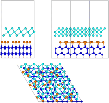 | ||
Fig. 5 The relaxed configuration of tellurene in a trilayer 1T-MoS2-like geometry adsorbed on the Si(111)- R30°-Sb surface in a slab geometry. Side and top views are shown. R30°-Sb surface in a slab geometry. Side and top views are shown. | ||
We calculated the formation energy of the trilayer adsorbed on the substrate with respect to bulk Te as
 | (1) |
![[thin space (1/6-em)]](https://www.rsc.org/images/entities/char_2009.gif) bulk is the energy per atom of bulk Te.
bulk is the energy per atom of bulk Te.
The resulting formation energy is 94 meV per atom which is positive because the energy gain due to the interaction of Te with the substrate is lower than the energy paid to form a trilayer from the bulk.
The adsorption energy of tellurene on the substrate with respect to the free-standing trilayer is estimated instead by
 | (2) |
The adsorption energy Eads = −59 meV per atom is negative due to the attractive interaction with the substrate with an energy gain with respect to the free-standing tellurene. The value of Eads is most probably an underestimation because of the strain experienced by the adsorbed tellurene due to the constraint of the supercell geometry which features a 3.6% misfit with respect to the equilibrium lattice parameter of the free-standing trilayer. We then estimated the energy cost of straining tellurene by optimizing the free-standing trilayer with the lattice parameters of the substrate (equivalent to a = 3.974 Å). The resulting strain energy with respect to the equilibrium lattice parameters of the free-standing trilayer is 29 meV per atom. By assuming that the same energy penalty is paid by tellurene adsorbed on the substrate, one would predict for tellurene adsorbed in an incommensurate manner on the substrate a formation energy of 65 meV per atom with respect to that of bulk Te (eqn (1)) and an adsorption energy of about −88 meV per atom with respect to that of the optimized free-standing trilayer.
This value of the adsorption energy is larger than the difference in energy between the Te(10![[1 with combining macron]](https://www.rsc.org/images/entities/char_0031_0304.gif) 0) and the 1T-MoS2-like geometries of the free-standing trilayer (68 meV per atom, see Section 3.2).
0) and the 1T-MoS2-like geometries of the free-standing trilayer (68 meV per atom, see Section 3.2).
One might thus conceive that the interaction with the substrate might change the hierarchy in energy among the different configurations of the free-standing trilayer.
In the next subsection we will therefore discuss the optimization of the trilayer of Te adsorbed on the substrate in the Te(10![[1 with combining macron]](https://www.rsc.org/images/entities/char_0031_0304.gif) 0) geometry.
0) geometry.
![[1 with combining macron]](https://www.rsc.org/images/entities/b_char_0031_0304.gif) 0) geometry.
For the reconstructed geometry of the Te(10
0) geometry.
For the reconstructed geometry of the Te(10![[1 with combining macron]](https://www.rsc.org/images/entities/char_0031_0304.gif) 0) structure (β geometry mentioned in ref. 8, see inset in Fig. 4) a commensuration with the substrate is not easy. A possibility is to align the a lattice parameter of tellurene with the a lattice parameter of the hexagonal unit cell in the geometry shown in Fig. 6 which corresponds to 3 × 2 cells of tellurene matched with a 2 a ×
0) structure (β geometry mentioned in ref. 8, see inset in Fig. 4) a commensuration with the substrate is not easy. A possibility is to align the a lattice parameter of tellurene with the a lattice parameter of the hexagonal unit cell in the geometry shown in Fig. 6 which corresponds to 3 × 2 cells of tellurene matched with a 2 a ×  rectangular supercell of the substrate. By considering the a and b equilibrium lattice parameters of tellurene in the Te(10
![[1 with combining macron]](https://www.rsc.org/images/entities/char_0031_0304.gif) 0) trilayer (a = 4.142 Å and b = 5.449 Å, see Section 3.2) the mismatch is as large as 5–6% along both the a and b directions.
0) trilayer (a = 4.142 Å and b = 5.449 Å, see Section 3.2) the mismatch is as large as 5–6% along both the a and b directions.
However, the misfit decreases to 1.2 and 1.3% along the two directions if we consider the unreconstructed trilayer with the helical chains at the equilibrium lattice parameters of a bi-trilayer found in previous DFT calculations28 (a = 4.36 Å and b = 5.81 Å, see Section 3.2). As a first attempt, we therefore considered the supercell geometry sketched in Fig. 6 with an initial configuration featuring helical Te chains as in the bulk (see Fig. 3).
The optimized geometry of tellurene adsorbed on the slab of the substrate is shown in Fig. 7. The Te chains are still present albeit slightly distorted, with the Te atoms two-fold coordinated. The average interplanar distance between the Sb and the innermost Te plane is 2.96 Å. The atomic positions in Cartesian coordinates and the cell edges of the slab are given in the ESI.†
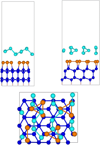 | ||
Fig. 7 Side and top views of the relaxed configuration of tellurene in the Te(10![[1 with combining macron]](https://www.rsc.org/images/entities/char_0031_0304.gif) 0) geometry on Si(111)- 0) geometry on Si(111)- R30°-Sb surface. R30°-Sb surface. | ||
We calculated the formation energy of the trilayer adsorbed on the surface with respect to bulk Te as given by eqn (1) (n = 18 for this geometry) which yields Eform =111 meV per atom. This value is larger than the formation energy obtained for the 1T-MoS2-like geometry reported in the previous section. This result confirms the higher stability of the latter configuration as it occurs for the free-standing trilayer. The adsorption energy of tellurene on the substrate with respect to that of the free-standing trilayer given by eqn (2) is instead Eads = −112 meV per atom for the Te(10![[1 with combining macron]](https://www.rsc.org/images/entities/char_0031_0304.gif) 0) geometry which suggests a stronger interaction between the trilayer and the substrate than for the 1T-MoS2-like geometry (−59 meV per atom, see Section 3.3.1). We must also consider that tellurene adsorbed on the surface is highly strained with respect to the equilibrium lattice parameter of the Te(10
0) geometry which suggests a stronger interaction between the trilayer and the substrate than for the 1T-MoS2-like geometry (−59 meV per atom, see Section 3.3.1). We must also consider that tellurene adsorbed on the surface is highly strained with respect to the equilibrium lattice parameter of the Te(10![[1 with combining macron]](https://www.rsc.org/images/entities/char_0031_0304.gif) 0) free-standing trilayer. We then calculated the strain energy from the energy difference between the trilayer at the equilibrium lattice parameter (β geometry of ref. 8) and at the lattice parameters commensurate with the substrate as given above. The resulting strain energy is 32 meV per atom. By assuming that the same energy penalty is paid by tellurene adsorbed on the substrate, one would predict for tellurene adsorbed in an incommensurate manner on the substrate a formation energy of 111–31 meV per atom = 80 meV per atom which is higher by only 15 meV per atom than that of tellurene adsorbed in the 1T-MoS2-like trilayer (65 meV per atom, see Section 3.3.1).
0) free-standing trilayer. We then calculated the strain energy from the energy difference between the trilayer at the equilibrium lattice parameter (β geometry of ref. 8) and at the lattice parameters commensurate with the substrate as given above. The resulting strain energy is 32 meV per atom. By assuming that the same energy penalty is paid by tellurene adsorbed on the substrate, one would predict for tellurene adsorbed in an incommensurate manner on the substrate a formation energy of 111–31 meV per atom = 80 meV per atom which is higher by only 15 meV per atom than that of tellurene adsorbed in the 1T-MoS2-like trilayer (65 meV per atom, see Section 3.3.1).
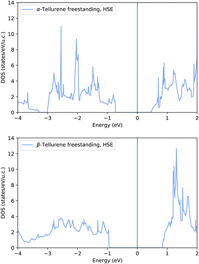
![[1 with combining macron]](https://www.rsc.org/images/entities/char_0031_0304.gif) 0) (β) phases of free-standing tellurene reported in Fig. 8 reproduces the band gap already found in ref. 8.
0) (β) phases of free-standing tellurene reported in Fig. 8 reproduces the band gap already found in ref. 8.
The DOS projected on the Te atoms 1T-MoS2-like (α) and (bottom panel) Te(10![[1 with combining macron]](https://www.rsc.org/images/entities/char_0031_0304.gif) 0) (β) phases of tellurene adsorbed on the Si(111)-
0) (β) phases of tellurene adsorbed on the Si(111)- R30°-Sb surface are shown in Fig. 9 and compared with the DOS of the corresponding free-standing phases. It turns out that the interaction with the surface leads to a substantial reduction of the band gap for both phases.
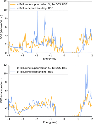 | ||
Fig. 9 Electronic density of states projected on the Te atoms of the (top panel) 1T-MoS2-like (α) and (bottom panel) Te(10![[1 with combining macron]](https://www.rsc.org/images/entities/char_0031_0304.gif) 0) (β) phases of tellurene adsorbed on the Si(111)- 0) (β) phases of tellurene adsorbed on the Si(111)- R30°-Sb surface. The DOS is computed with the HSE06 functional on a single special point with a smearing of the Kohn–Sham energy of 0.015 Ry. The DOS of the adsorbed tellurene is compared with that of the free-standing tellurene in Fig. 8. The DOS are aligned at the top of the valence band. R30°-Sb surface. The DOS is computed with the HSE06 functional on a single special point with a smearing of the Kohn–Sham energy of 0.015 Ry. The DOS of the adsorbed tellurene is compared with that of the free-standing tellurene in Fig. 8. The DOS are aligned at the top of the valence band. | ||
4 Conclusions
In summary, we reported on DFT calculations of the adsorption of a trilayer tellurene on the Si(111)- R30°-Sb surface. This surface has been chosen here as a suitable substrate for the growth of a high quality tellurene film directly on Si surfaces for integration with silicon technology. In fact, it has been shown in the literature that different telluride compounds, such as GeTe16 and layered Sb2Te3 and (GeTe)n (Sb2Te3)m,17 can be grown on this substrate as quasi single-crystalline thin films with minimal rotational disorder of the crystalline domains which is expected to improve the electrical properties of the film. Our DFT calculations reveal that the adsorption energy is substantially different for the two phases, α and β, of free-standing tellurene. Although in the free-standing geometry the α phase is 68 meV per atom lower in energy than the β phase, the adsorption energy partially compensates this energy difference. In spite of the many uncertainties due to the constraints of commensuration with the substrate, DFT calculations suggest that tellurene in the α phase, which consists of a trilayer 1T-MoS2-like geometry, becomes only marginally (15 meV per atom) more stable than the β geometry when adsorbed on the Si(111)-
 R30°-Sb surface. This result supports the experimental pieces of evidence that the formation of the α or β phases depends on the substrate the tellurene is grown on. On the Si(111)-
 R30°-Sb surface, which is here suggested as a suitable substrate for the integration of tellurene on silicon in analogy with other tellurides, the energy difference of the two phases is particularly tiny and the prevalence of one trilayer phase with respect to the other might thus be strongly affected by the kinetics effects and deposition conditions. Obviously, the Te(10
![[1 with combining macron]](https://www.rsc.org/images/entities/char_0031_0304.gif) 0) geometry will finally prevail by increasing the number of Te layers.
0) geometry will finally prevail by increasing the number of Te layers.
Author contributions
Conceptualization: M. B. and S. C.; investigation: S. I., D. D., M. B., and S. C.; validation and data curation: S. I., D. D., D. C., and M. B.; methodology and supervision: M. B.; writing—original draft: S. I. and M. B.; writing—review & editing: S. I., M. B., D. C., and S. C.Conflicts of interest
There are no conflicts to declare.Notes and references
- C. Grazianetti, C. Martella and A. Molle, Phys. Status Solidi RRL, 2020, 14, 1900439 CrossRef CAS.
- C. Adenis, V. Langer and O. Lindqvist, Acta Crystallogr., 1989, C45, 941–942 CAS.
- H. O. H. Churchill, G. J. Salamo, S.-Q. Yu, T. Hironaka, X. Hu, J. Stacy and I. Shih, Nanoscale Res. Lett., 2017, 12, 488 CrossRef PubMed.
- Y. Wang, G. Qiu, R. Wang, S. Huang, Q. X. Wang, Y. Liu, Y. Du, W. A. G. III, M. J. Kim, X. Xu, P. D. Ye and W. Wu, Nat. Electron., 2018, 1, 228–236 CrossRef.
- X. Huang, J. Guan, Z. Lin, B. Liu, S. Xing, W. Wang and J. Guo, Nano Lett., 2017, 17, 4619–4623 CrossRef CAS PubMed.
- R. Tran, Z. Xu, B. Radhakrishnan, D. Winston, W. Sun, K. A. Persson and S. P. Ong, Sci. Data, 2016, 3, 1–13 Search PubMed.
- Q. Wang, M. Safdar, K. Xu, M. Mirza, Z. Wang and J. He, ACS Nano, 2014, 8, 7497–7505 CrossRef CAS PubMed.
- Z. Zhu, X. Cai, S. Yi, J. Chen, Y. Dai, C. Niu, Z. Guo, M. Xie, F. Liu, J.-H. Cho, Y. Jia and Z. Zhang, Phys. Rev. Lett., 2017, 119, 106101 CrossRef PubMed.
- J. Chen, Y. Dai, Y. Ma, X. Dai, W. Ho and M. Xie, Nanoscale, 2017, 9, 15945–15948 RSC.
- A. Apte, E. Bianco, A. Krishnamoorthy, S. Yazdi, R. Rao, N. Glavin, H. Kumazoe, V. Varshney, A. Roy, F. Shimojo, E. Ringe, R. K. Kalia, A. Nakano, C. S. Tiwary, P. Vashishta, V. Kochat and P. M. Ajayan, 2D Mater., 2018, 6, 015013 CrossRef.
- Z. Yan, H. Yang, Z. Yang, C. Ji, G. Zhang, Y. Tu, G. Du, S. Cai and S. Lin, Small, 2022, 18, 2200016 CrossRef CAS PubMed.
- N. Youngblood and M. Li, Nanophotonics, 2017, 6, 1205 CAS.
- H. Li, L. Gao, H. Li, G. Wang, J. Wu, Z. Zhou and Z. Wanga, Appl. Phys. Lett., 2013, 102, 074106 CrossRef.
- G. Zhang, H. Qin, J. Teng, J. Guo, Q. Guo, X. Dai, Z. Fang and K. Wu, Appl. Phys. Lett., 2009, 95, 053114 CrossRef.
- N. Bansal, Y. S. Kim, E. Edrey, M. Brahlek, Y. Horibe, K. Iida, M. Tanimura, G.-H. Li, T. Feng and H. D. Li, et al. , Thin Solid Films, 2011, 520, 224 CrossRef CAS.
- R. Wang, J. E. Boschker, D. D. S. Emilie Bruyer, S. Picozzi, K. Perumal, A. Giussani, H. Riechert and R. Calarco, J. Phys. Chem. C, 2014, 118, 29724–29730 CrossRef CAS.
- J. E. Boschker, J. Momand, V. Bragaglia, R. Wang, K. Perumal, A. Giussani, B. J. Kooi, H. Riechert and R. Calarco, Nano Lett., 2014, 14, 3534 CrossRef CAS PubMed.
- L. H. X. Kou and K. L. Wang, Phys. Status Solidi RRL, 2013, 7, 50 CrossRef.
- N. V. Tarakina, S. Schreyeck, T. Borzenko, C. Schumacher, G. Karczewski, K. Brunner, C. Gould, H. Buhmann and L. W. Molenkamp, Cryst. Growth Des., 2012, 12, 1913 CrossRef CAS.
- P. Giannozzi, S. Baroni, N. Bonini, M. Calandra, R. Car, C. Cavazzoni, D. Ceresoli, G. L. Chiarotti, M. Cococcioni, I. Dabo, A. D. Corso, S. de Gironcoli, S. Fabris, G. Fratesi, R. Gebauer, U. Gerstmann, C. Gougoussis, A. Kokalj, M. Lazzeri, L. Martin-Samos, N. Marzari, F. Mauri, R. Mazzarello, S. Paolini, A. Pasquarello, L. Paulatto, C. Sbraccia, S. Scandolo, G. Sclauzero, A. P. Seitsonen, A. Smogunov, P. Umari and R. M. Wentzcovitch, J. Phys.: Condens. Matter, 2009, 21, 395502 CrossRef PubMed.
- P. Giannozzi, O. Andreussi, T. Brumme, O. Bunau, M. B. Nardelli, M. Calandra, R. Car, C. Cavazzoni, D. Ceresoli, M. Cococcioni, N. Colonna, I. Carnimeo, A. D. Corso, S. de Gironcolin, P. Delugas, R. A. D. S. Jr., A. Ferretti, A. Floris, G. Fratesi, G. Fugallo, R. Gebauer, U. Gerstmann, F. Giustino, T. Gorni, J. Jia, M. Kawamura1, H.-Y. Ko, A. Kokalj, E. Küçükbenli, M. Lazzeri, M. Marsili, N. Marzari, F. Mauri, N. L. Nguyen, H.-V. Nguyen, A. O. de la Roza, L. Paulatto, S. Poncé, D. Rocca, R. Sabatini, B. Santra, M. Schlipf, A. P. Seitsonen, A. Smogunov, I. Timrov, T. Thonhauser, P. Umari, N. Vast, W. Xifan and S. Baroni, J. Phys.: Condens. Matter, 2017, 29, 465901 CrossRef CAS PubMed.
- J. P. Perdew, K. Burke and M. Ernzerhof, Phys. Rev. Lett., 1996, 77, 3865–3868 CrossRef CAS PubMed.
- S. Grimme, J. Comput. Chem., 2006, 27, 1787–1799 CrossRef CAS PubMed.
- H. J. Monkhorst and J. D. Pack, Phys. Rev. B: Solid State, 1976, 13, 5188–5192 CrossRef.
- C. Kittel, in Introduction to Solid State Physics, Wiley; New York, 5th edn, 1976 Search PubMed.
- S. Bengió, M. Martin, J. Avila, M. C. Asensio and H. Ascolani, Phys. Rev. B: Condens. Matter Mater. Phys., 2002, 65, 205326 CrossRef.
- R. Keller, W. B. Holzapfel and H. Schulz, Phys. Rev. B: Solid State, 1977, 16, 4404–4412 CrossRef CAS.
- J. Qiao, Y. Pan, F. Yang, C. Wang, Y. Chai and W. Ji, Sci. Bull., 2018, 63, 159–168 CrossRef CAS.
- J. Heyd, G. E. Scuseria and Z. Ernzerhof, J. Chem. Phys., 2003, 118, 8207 CrossRef CAS.
- D. K. Sang, B. Wen, S. Gao, Y. Zeng, F. Meng, Z. Guo and H. Zhang, Nanomaterials, 2019, 9, 1075 CrossRef CAS PubMed.
Footnotes |
| † Electronic supplementary information (ESI) available: Atomic positions of tellurene adsorbed on the silicon surface in Cartesian coordinates. See DOI: https://doi.org/10.1039/d2cp01759h |
| ‡ Present address: Institute of Solid-State Electronics, TU Wien, Gusshausstrasse 25-25a, 1040 Vienna, Austria. E-mail: stefania.isceri@tuwien.ac.at |
| § Present address: Leonardo S. p. A., Piazza Monte Grappa 4, 00195, Roma, Italy. |
| This journal is © the Owner Societies 2022 |


