Superior electrical conduction of a water repelling 3D interconnected nano-network†
Received
23rd November 2017
, Accepted 24th January 2018
First published on 24th January 2018
Abstract
A three-dimensional (3D) network of interconnected nanowires of functional materials possesses huge potential for device fabrication since it hinders sluggish interfacial charge carrier transport owing to reduced contact resistance. In the present work, the formation of a highly porous 3D interconnected nano-network by Na+ ion irradiation is demonstrated. The mechanism of solid junction formation at very low energy is established using the results obtained from TRI3DYN computer simulation studies. The formation of a 3D interconnected network resulted in a significant improvement in the electrical conduction as compared to that observed for the pristine nanotube mesh. Further, contact angle measurement shows a transition from “superhydrophilic” nature, as observed for pristine nanotubes, to “superhydrophobic” nature for the 3D nano-network. The superhydrophobicity of the 3D nano-network is expected to find application in miniaturized electronic devices, wherein water condensation and related effects such as short-circuits and erroneous signal output can be significantly minimized.
1. Introduction
In past decades a major focus was on the growth and fabrication of nanostructured functional materials with different morphologies. At present emphasis is being given to using these nanostructured materials to fabricate devices. For such device fabrication, one of the most important aspects would be the joining of individual nanostructures. It is believed that the most flexible way of fabricating a nanoscale junction is a bottom-up approach.1,2 Many elaborate studies have been performed on the joining of metal3,4 and carbon based5,6 nanostructured components. Very recently, our group has shown that ion irradiation can be used effectively for joining ceramic nanowires, producing a 2D interconnected large-scale network.7–9 An important challenge still remains to realize a stable 3D interconnected network of ceramic nanomaterials. To the best of our knowledge until now there has been no report of the production of a 3D interconnected nano-network of ceramic nanomaterials by ion irradiation. A handful of papers are available on 3D nanomaterials which have been grown using mainly chemical routes for carbon based10–13 and a few ceramics based14,15 nanomaterials. Ion irradiation has been used to fabricate 3D folding sheets2 and a 3D fin array.16 The present work on a 3D interconnected nano-network is expected to have versatile applications for miniaturized electronic devices, sensors, filters, catalysts etc. The formation of interconnections reduces contact resistance, and as a result an enhancement in charge carrier transport is expected, which in turn will enhance the efficiency of the nanodevices. The large specific surface area or the improved surface area to volume ratio of the 3D network structure may make it useful as a catalyst support.
In this work, we report the formation of a 3D assembly of hydrogen titanate nanotubes upon ion irradiation. Irradiation of the as-prepared nanotubes with 5 keV Na+ ions at different ion fluences resulted in the formation of a complex interconnected network, establishing a 3D porous structure. I–V measurements revealed that the 3D interconnected nano-network structures exhibit significant enhancement of current conduction as compared to that of the pristine sample. Remarkably, the as-prepared hydrogen titanate nanotubes were superhydrophilic in nature, while the 3D nano-network structure turns out to be superhydrophobic. Our study shows that the fabrication of a 3D interconnected nano-network using ion irradiation is simple, speedy, easily controllable and can be performed at a large scale.
2. Experimental details
2.1 Synthesis of nanotubes
Hydrogen titanate nanotubes (HTNT) were synthesised hydrothermally. For this synthesis, 99.9% pure TiO2 (anatase) powder was dissolved in 10 M NaOH solution and stirred continuously for over 3 days. The solution was then put in an autoclave and the growth was carried out at a temperature of 150 °C for about 12 h in a hot-air oven. The product obtained in a powder form was further washed multiple times using dilute hydrochloric acid to remove sodium ions, which produces hydrogen titanate nanotubes (HTNT) as the final product. The HTNT powder was finally washed with deionized water and dried. In order to make the coating, the HTNTs were dispersed in ethanol and ultrasonicated for 30 min. The ultrasonicated HTNT were dropcasted using a fine-tip pipette on pre-cleaned silicon substrates and dried in air.
2.2 Ion irradiation and characterizations
The irradiation was performed in an ion–solid interaction setup developed in-house at IIT Bhubaneswar.17 Na+ ions of energy 5 keV were derived from an alkali metal ion source (Kimball Physics Inc.) to irradiate the samples at different ion fluences. The beam was uniform, having a diameter of about 1 cm and a steady beam current of 1 μA. The samples coated on the silicon substrate were mounted on an indigenously developed 5-axis manipulator. The pre- and post-irradiated samples were characterized using a scanning electron microscope (SEM, Zeiss Merlin Compact Gemini) to analyze the surface morphology. A Raman scattering study was performed using a Jobin Yvon T64000 Micro-Raman spectrometer equipped with an inverted microscope. I–V characteristics were studied using a two-probe method. Two tungsten probes were connected to the surface of the sample using silver paste. The current was measured by varying the voltage in the range of ±1 V using a Keithley 6517B electrometer. The wetting properties of pre- and post-irradiated samples were studied by measuring contact angles of sessile drops of Milli-Q water using a contact angle meter (OCA15EC, Dataphysics) at room temperature. The contact angle measurements were done at three different locations on each sample to check the consistency.
3. Simulation details
The computer simulation of ion irradiation effects on 3D HTNT was performed using TRI3DYN, which is based on the Binary Collision Approximation (BCA) and treated using a Monte Carlo concept.18,19 Unlike the Transport of Ions in Matter (TRIM)20 program, the current simulation can be performed for a 3D structure with an arbitrary shape, which predicts more accurate post-collision consequences. The target was comprised of volume elements of size 400 (depth) × 600 × 600 nm3 and total of 40 × 60 × 60 voxels with periodic y–z boundaries. A uniform and broad beam of Na+ ions (atomic number 11 and atomic mass 22.98 u) was used as the projectile at an energy of 5 keV and ion fluences of 5 × 10¹⁵ and 1 × 10¹⁶ ions per cm2, respectively.
4. Results and discussions
The as-prepared HTNT show a 3D assembly of loosely bound nanotubes, as observed under a scanning electron microscope (Fig. 1). The size of the 3D clusters is typically in the range between 1 and 10 μm. The transmission electron microscope images of a few nanotubes taken from the 3D cluster reveal that the individual HTNT units are highly crystalline in nature with a typical diameter of 15 ± 5 nm and a length of about 1–2 μm. It is further evident from the figure that the nanotubes are loosely touching each other, possibly due to van der Waals type interactions and, apparently, there is no solid mechanical joining.
 |
| | Fig. 1 (a and b) Scanning electron micrographs and (c) high resolution TEM image of the 3D pristine hydrogen titanate nanotube assembly. | |
The pristine 3D assemblies were irradiated with 5 keV Na+ ions at different ion fluences. At an ion fluence of 1 × 10¹⁶ ions per cm2 the nanotubes are welded and form large-scale junctions (Fig. 2(a) and (b)) yielding a 3D interconnected network with solid junctions. At a larger ion fluence of 2 × 10¹⁶ ions per cm2 the junction areas thicken, as shown in Fig. 2(c) and (d). The 3D network structure is comprised of pores of sizes in the range of 20–200 nm. This observation clearly implies that using low-energy ions a 3D welded nano-network with a porous structure can be achieved easily. The joining of the 3D network at a fluence of 2 × 10¹⁶ ions per cm2 is further investigated using TEM. This apparently shows two effects: namely, nanotubes have been converted into solid nanowires and a clear physical join persists between them (Fig. 3).
 |
| | Fig. 2 SEM micrographs of 3D HTNT samples irradiated with 5 keV Na+ ions at fluences of 1 × 10¹⁶ ions per cm2 (a), (b) and 2 × 10¹⁶ ions per cm2 (c), (d). | |
 |
| | Fig. 3 High resolution TEM image of 3D HTNT irradiated with 2 × 10¹⁶ ions per cm2 showing welded junctions. | |
The joining mechanism at this low energy, where thermal spike related effects are less likely, is investigated by employing TRI3DYN simulations. The collisional effects can be realized through this simulation while looking into the evolutions of atomic fractions of the nanotubes before and after irradiation. For instance, in Fig. 4(a) and (b), the titanium atomic fraction is shown on two HTNT oriented perpendicular to each other in a 3D geometry. With an increase in ion fluence from 5 × 10¹⁵ up to 1 × 10¹⁶ ions per cm2 (Fig. 4(c) and (d)) a consistent downward flow (along the direction of ions) of titanium atoms occurs due to recoils and sputtering. The ion irradiation further creates dangling bonds due to collision-induced defects on the surface of the nanotubes. Thus, the amassed atoms in between two nanotubes bridge the gap by saturating the dangling bonds and establish a solid join.9 The simulation further shows that the hollow part of the nanotubes is gradually filled with atoms, producing a solid wire-like structure, as is also evident in the TEM image (Fig. 3). The simulation predicts a change in the Ti/O ratio with increasing ion fluence (Fig. 5(a) and (b)). It is apparent that the Ti/O ratio increases mostly in the lower nanotubes of the given geometry from an initial 0.42 to about 0.8, which indicates the role of preferential sputtering and surface diffusion.8,9 Such altered abundances of Ti and O may trigger the formation of a new phase of titanium oxide. The simulation also predicts that some negligible amount of silicon gets deposited only at the bottom of the nanotubes (Fig. 5(c) and (d)). Silicon atoms from the substrate are ejected due to sputtering, which is caused by primary ions as well as by recoiled atoms. The sputtered-out silicon atoms are slow enough and, therefore, they settle at the bottom part of the nanotubes. TRI3DYN simulation shows that the atomic fraction of silicon at the bottom of the nanotubes is nearly 0.2. The primary Na+ ions travel across the nanotube walls and suffer successive collisions with the lattice atoms and lose energy mostly through nuclear stopping (i.e. elastic collision). We have performed a calculation using the TRIM20 program to simulate the collision details, which shows that the Na+ ions have range of about 8 nm. Since the average wall thickness of a nanotube is 5 nm, the ions are mostly stopped on the opposite side of the wall of entry as well as just outside the nanotube: i.e. in the junction areas. The TRI3DYN simulation confirms the presence of most of the sodium atoms at the sidewall and junction areas, as seen in Fig. 5(e) and (f). The simulation results in Fig. 4 and 5 further show that the bottoms of the nanotubes are physically welded to the substrate, which offers the possibility that the irradiated titanate surface can be used as a coating material.
 |
| | Fig. 4 The surface contours as obtained from the TRI3DYN computer simulation show Ti atomic fractions: (a, b) for pristine sample, (c, d) and (e, f) after 5 keV Na+ irradiation at ion fluences of 5 × 10¹⁵ ions per cm2 and 1 × 10¹⁶ ions per cm2, respectively. The outer diameter of the nanotubes is 15 nm with a wall thickness of 5 nm. The Ti atomic fraction is shown in the range from 0 to 0.5. | |
 |
| | Fig. 5
X–Y cut-through the axis of the upper tube. The Ti/O atomic ratio (a, b); the silicon atomic fraction (c, d) and sodium atomic fractions (e, f) are shown for two different ion fluences of 5 × 10¹⁵ ions per cm2 (left-hand figures) and 1 × 10¹⁶ ions per cm2 (right-hand figures). | |
The irradiation-induced formation of a new phase is also apparent in the Raman scattering study. As shown in Fig. 6, the pristine sample shows characteristic peaks at around 198, 272. 458 and 678 cm−1 that correspond to the hydrogen titanate nanotubes. At the largest ion fluence used in this study several strong peaks appear. Apart from the peak at 272 cm−1 for hydrogen titanate, peaks around 440 and 612 cm−1 correspond to the rutile phase and the peak around 150 cm−1 corresponds to the anatase phase of titanium dioxide.21
 |
| | Fig. 6 Raman scattering spectra of pristine and irradiated (2 × 10¹⁶ ions per cm2) samples. | |
4.1 Electrical property
I–V measurements for pristine and irradiated 3D samples show interesting aspects (Fig. 7). For pristine HTNT the current has been measured in the voltage range of −1 to +1 V, which yields a nonlinear curve with current in the range of 3–5 μA (Fig. 7(a)). The current increases drastically at an ion fluence where large-scale welding is formed and it reaches about 10 mA at a fluence of 2 × 10¹⁶ ions per cm2 (Fig. 7(b)). The distance between the two tungsten probes was fixed at 4 mm for both pristine and irradiated samples. Each probe has a width about 2 mm. While the conductivity of the pristine sample is estimated to be 7.86 S m−1 at 0.5 V, the value for the irradiated sample is 2.19 × 10⁴ S m−1, which is about four orders of magnitude larger than that of the pristine sample. For pristine 3D mesh the nanotubes are loosely connected to each other, which leads to the high contact resistance. In contrast, for the irradiated 3D sample, the nanotubes are physically welded, providing good contacts with a large area, as shown schematically in Fig. 8. Furthermore, the nanotubes are converted into solid nanowires providing high cross section areas for the conduction of charge carriers. Thus the combined effect of welding and conversion into solid nanowires enhances the electrical conductivity and reduces the overall resistance.6 At high ion fluence (2 × 10¹⁶ ions per cm2) the I–V curve tends to become more linear with no barrier potential. Since the work function of silver (4.3 eV22,23) is comparable with the electron affinity of titanium oxide, which is in the range of 3.9–4.8 eV,24–26 this leads to a zero barrier height with almost no rectifying action in this case.
 |
| | Fig. 7
I–V curves for pristine (a) and irradiated 3D hydrogen titanate at an ion fluence of 2 × 10¹⁶ ions per cm2 (b). | |
 |
| | Fig. 8 Schematic showing reduced contact resistance and increase in conduction area after the ion irradiation. | |
4.2 Wetting property
The interaction of water droplets with both pristine and irradiated 3D samples has been studied using contact angle measurements. The water droplet on the pristine sample disappears extremely fast, as shown in Fig. 9. The time evolution of the droplet has been captured from the initial stage, i.e. before touching the surface. Within 0.15 s the water droplet flattens on the surface with a contact angle close to 0° and it vanishes completely before 5 s. Thus the pristine sample turns out to be superhydrophilic in nature. This, however, changes drastically upon ion irradiation. As shown in Fig. 10, the contact angle of water increases with increasing ion fluence. At an ion fluence of 8 × 10¹⁵ ions per cm2 the sample surface becomes hydrophilic with a contact angle of 53° ± 2° (Fig. 10(a)) from an initial superhydrophilic surface. At an increased ion fluence of 1 × 10¹⁶ ions per cm2 the sample surface becomes hydrophobic with a contact angle of 105° ± 2° (Fig. 10(b)). At the highest ion fluence of 2 × 10¹⁶ ions per cm2 used in this work, the surface turns superhydrophobic with a contact angle of 150° ± 2.5° (Fig. 10(c)). There was almost no change in the contact angle of the irradiated sample (i.e. superhydrophobic nature) measured two months after the irradiation (Fig. 10(d)). We have delved into possible reasons for such drastic changes.
 |
| | Fig. 9 Optical image of water droplet on pristine 3D hydrogen titanate assembly at 0 (a), 0.14 (b), 1.4 (c) and 4.9 s (d). | |
 |
| | Fig. 10 Optical image of water droplet on irradiated 3D hydrogen titanate network for ion fluences 8 × 10¹⁵ ions per cm2 (a), 1 × 10¹⁶ ions per cm2 (b), immediately (c) and two months (d) after the ion irradiation at a fluence of 2 × 10¹⁶ ions per cm2. | |
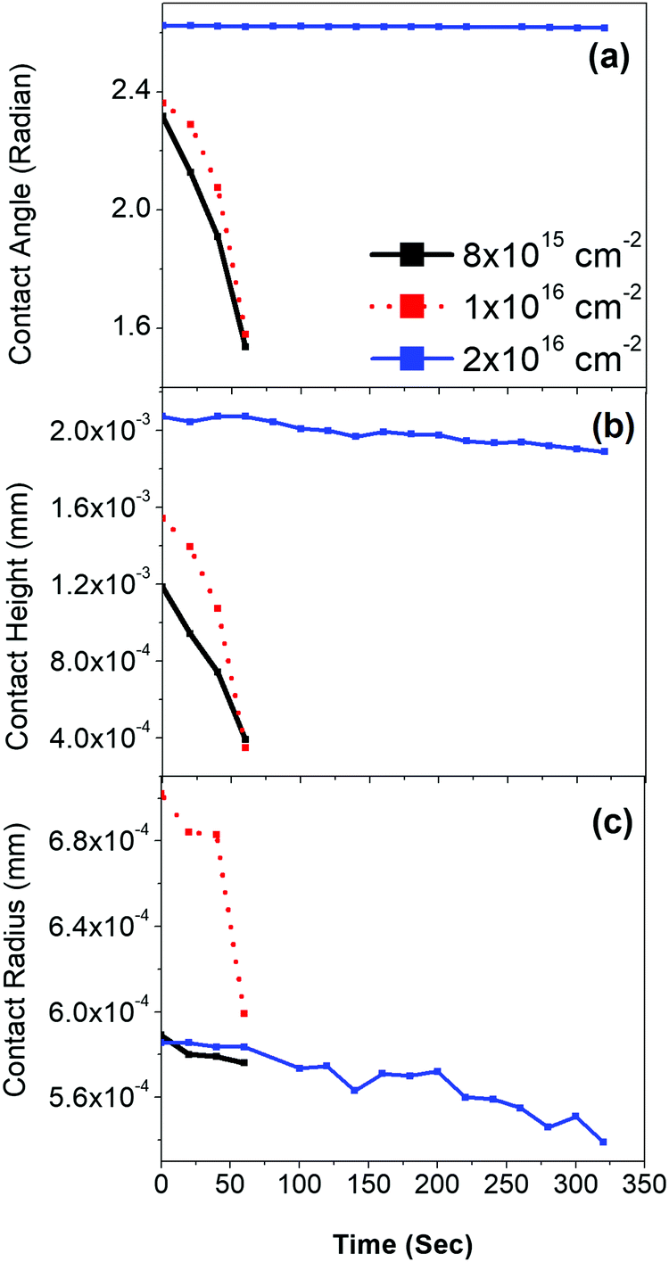
Usually the wetting property depends on the chemical property of the surface as well as on the microstructures present on the surface. It is known that a monoclinic hydrogen titanate structure contains lot of –OH groups on the surface.27,28 Thus the presence of OH groups in a pristine sample attracts water molecules, leading to the superhydrophilic nature of the surface. On the other hand, irradiated samples contain rutile and anatase phases, as evident from Raman spectroscopy, which usually yields a hydrophobic surface.29,30 However, a significant contribution towards a strong water repelling nature comes from the 3D porous network. Usually the roughness of a nanostructured surface leads to a hydrophobic nature, termed a Wenzel surface.31,32 The other type is a Cassie–Baxter type surface, where trapped air in the nanostructure pushes back the water, leading to the superhydrophobic nature of the surface.32,33 The welded network traps air, which forms a Cassie state, resulting in a hydrophobic nature. With increasing ion fluence, the welding occurs over a large scale and more trapped air pockets are produced, which leads to the superhydrophobic nature of the surface. We have studied the time evolution of water droplets on the irradiated surfaces for different ion fluences, as shown in Fig. 11. It is evident that for lower ion fluences (8 × 10¹⁵ and 1 × 10¹⁶ ions per cm2) the contact parameters, such as contact angle (θ), contact height (h) and contact radius (rb), drop drastically to about 50–70% within 2 min. Whereas, at the highest fluence of 2 × 10¹⁶ ions per cm2, θ, h and rb remain almost constant for a long time.
 |
| | Fig. 11 Time dynamics of contact angle (a), contact height (b) and contact radius (c) of 3D hydrogen titanate samples irradiated at different ion fluences. | |
The diffusion coefficient (D) was calculated using Fick's law of diffusion for a sessile water droplet.33,34 For the highest fluence used, this yields a value of (3.13 ± 0.52) × 10−5 m2 S−1, which is comparable with the normal evaporation of water droplets into the environment at room temperature.35 This implies that the irradiated 3D surface acts as a good water repellent. We have further tested the wetting behaviour of the nanowelded surface with saline water (concentration 1%), which showed a superhydrophobic character with a contact angle of about 151° (figure not shown). Thus the water repelling property of the irradiated surface is retained for both normal water and salted water. It may be interesting to note that usually the sodium based compounds are hygroscopic in nature. The network structure supersedes the water-attraction nature of sodium and makes the sample superhydrophobic. In principle, the amount of sodium implanted is tiny and it is mostly inside the surface with an approximate range of 8 nm (as obtained from TRIM simulation). Therefore, sodium plays almost no role in the wetting behaviour of the sample. The dynamics of interaction of the water droplets with the present superhydrophilic and superhydrophobic surfaces are provided in the form of videos in the ESI† as V1 and V2, respectively.
5. Conclusions
In conclusion, low-energy ion irradiation is used as a tool to fabricate a well-interconnected 3D nano-network of titanium oxide based nanowires. The Na+ ion irradiation leads to the formation of nanowires from hollow nanotubes and triggers solid mechanical joining between them. The 3D network structure offers a highly porous structure and is expected to have a large surface area as well as volume. The interconnected network shows about four orders of magnitude enhancement in electrical conductivity compared to that of the pristine sample, which is attributed to the physical joining and the conversion into solid nanowires. Taking into consideration the high surface area and volume with better conduction of charge carriers, this 3D interconnected nano-network could be a potential candidate for sensors or filtering applications. The water contact angle measurements show that the pristine hydrogen titanate nanotubes are superhydrophilic in nature. A drastic transition takes place upon irradiation with Na+ ions. The surface gradually becomes hydrophobic and finally turns superhydrophobic at larger ion fluences. This wetting property provides an advantage for this structure for use as a water-borne corrosion resistive coating.
Conflicts of interest
There are no conflicts to declare.
Acknowledgements
S. C. and N. R. acknowledge the financial support from Board of Research in Nuclear Sciences (DAE) for Grant No. 37(3)/14/19/2016-BRNS. S. C. is also thankful to SERB, DST for grant no. EMR/2017/000509. Authors are grateful to Dr P. K. Sahu for facilitating the electrical property measurements and I. Thakur for helping in wetting property measurements.
References
- H. Yan,
et al.
, Nature, 2011, 470(7333), 240–244 CrossRef CAS PubMed.
- W.-H. Kim,
et al.
, ACS Nano, 2016, 10(4), 4451–4458 CrossRef CAS PubMed.
- Z. Gu,
et al.
, Langmuir, 2007, 23(3), 979–982 CrossRef CAS PubMed.
- E. C. Garnett,
et al.
, Nat. Mater., 2012, 11(3), 241–249 CrossRef CAS PubMed.
- G. Seth Roberts and P. Singjai, Nanoscale, 2011, 3(11), 4503 RSC.
- J. S. Woo,
et al.
, Sci. Rep., 2014, 4, 4808 Search PubMed.
- S. Dhal,
et al.
, Nanotechnology, 2015, 26(23), 235601 CrossRef PubMed.
-
S. Dhal, et al., AIP Conference Proceedings, AIP Publishing, 2017, vol. 1832, p. 80091 Search PubMed.
- S. Dhal,
et al.
, Cryst. Growth Des., 2017, 17(5), 2660–2666 CAS.
- D. P. Hashim,
et al.
, Sci. Rep., 2012, 2, 363 CrossRef PubMed.
- P. M. Sudeep,
et al.
, ACS Nano, 2013, 7(8), 7034–7040 CrossRef CAS PubMed.
- S. Ozden,
et al.
, Carbon, 2017, 119, 142–149 CrossRef CAS.
- J. Yan,
et al.
, Adv. Funct. Mater., 2017, 27, 22 Search PubMed.
- Bin Liu and Hua Chun Zeng, J. Am. Chem. Soc., 2004, 126(51), 16744–16746 CrossRef CAS PubMed.
- Y. Xia,
et al.
, J. Alloys Compd., 2017, 705, 58–63 CrossRef CAS.
- C.-L. Wu,
et al.
, Nano Lett., 2016, 17(1), 249–254 CrossRef PubMed.
- P. Das,
et al.
, Nucl. Instrum. Methods Phys. Res., Sect. B, 2017, 413, 31–36 CrossRef CAS.
- W. Möller,
et al.
, Nucl. Instrum. Methods Phys. Res., Sect. B, 2014, 322, 23–33 CrossRef.
-
W. Eckstein, Springer Series in Materials Science, Computer Simulation of Ion-Solid Interactions, Springer-Verlag, Berlin, Heidelberg, 1991 Search PubMed.
-
J. F. Ziegler and J. P. Biersack, The Stopping and Range of Ions in Matter, Treatise on Heavy-Ion Science, Springer US, Boston, MA, 1985, pp. 93–129 Search PubMed.
- Y. Swamy,
et al.
, Appl. Phys. Lett., 2006, 89(16), 1–4 CrossRef.
- A. W. Dweydari,
et al.
, Phys. Status Solidi, 1975, 27(1), 223–230 CrossRef CAS.
- H. B. Michaelson, J. Appl. Phys., 1977, 48(11), 4729–4733 CrossRef CAS.
- D. O. Scanlon,
et al.
, Nat. Mater., 2013, 12(9), 798–801 CrossRef CAS PubMed.
- K. D. Schierbaum,
et al.
, Sens. Actuators, B, 1991, 4(1–2), 87–94 CrossRef CAS.
- R. Könenkamp,
et al.
, Mater. Sci. Eng., B, 2000, 69, 519–521 CrossRef.
- S. Chatterjee,
et al.
, J. Nanomater., 2014, 2014, 328618 Search PubMed.
- A. Liu,
et al.
, Anal. Chem., 2005, 77(24), 8068–8074 CrossRef CAS PubMed.
- R. Wang,
et al.
, J. Phys. Chem. B, 1999, 103(12), 2188–2194 CrossRef CAS.
- X. Peng,
et al.
, Appl. Phys. A: Mater. Sci. Process., 2005, 80(3), 473–476 CrossRef CAS.
- R. N. Wenzel, Ind. Eng. Chem., 1936, 28(8), 988–994 CrossRef CAS.
- S. Dhal,
et al.
, Soft Matter, 2015, 11(47), 9211–9217 RSC.
- A. B. D. Cassie and S. Baxter, Trans. Faraday Soc., 1944, 40, 546–551 RSC.
- Y.-S. Yu,
et al.
, J. Colloid Interface Sci., 2012, 365(1), 254–259 CrossRef CAS PubMed.
-
R. C. Weast, et al., CRC Handbook of Chemistry and Physics, CRC Press, Boca raton FL, 1989, vol. 1990 Search PubMed.
Footnote |
| † Electronic supplementary information (ESI) available: The videos for time variations of water droplet on the surfaces of pristine hydrogen titanate mesh (V1) and the irradiated 3D network sample (V2) are provided. See DOI: 10.1039/c7tc05374f |
|
| This journal is © The Royal Society of Chemistry 2018 |
Click here to see how this site uses Cookies. View our privacy policy here. 
 c,
Niranjan
Ramgir
d and
Shyamal
Chatterjee
c,
Niranjan
Ramgir
d and
Shyamal
Chatterjee