
 Open Access Article
 This Open Access Article is licensed under a
 Creative Commons Attribution 3.0 Unported Licence
Reversible stress-induced doping and charge trap generation in IDT-BT EGOFETs†
Axel
Luukkonen
 a,
Jonas
Jern
a,
Qiao
He
b,
Martin
Heeney
bc and
Ronald
Österbacka
*a
a,
Jonas
Jern
a,
Qiao
He
b,
Martin
Heeney
bc and
Ronald
Österbacka
*a
aÅbo Akademi University, Faculty of Science and Engineering, Henrikinkatu 2, Turku 20500, Finland. E-mail: ronald.osterbacka@abo.fi
bImperial College London, Department of Chemistry and Centre for Processable Electronics, London W12 0BZ, UK
cKAUST Solar Center (KSC), Physical Sciences and Engineering Division (PSE), King Abdullah University of Science and Technology (KAUST), Thuwal 23955-6900, Saudi Arabia
First published on 2nd January 2025
Abstract
Electrolyte-gated organic field-effect transistors (EGOFETs) have great potential for highly sensitive and affordable biosensors due to their low operating voltages and adaptable device geometry, facilitated by the large double layer capacitance in the electrolyte. While high performance biosensors have been attained using a variety of materials and device structures, the operational stability of EGOFETs remains poorly understood. Polythiophenes such as P3HT and pBTTT are the most commonly used organic semiconductors in these devices owing to their high hydrophobicity and well-known film and transport properties. However, in conventional OFETs they have been surpassed both with regards to performance and stability. Poly[2,1,3-benzothiadiazole-4,7-diyl-co-4,4,9,9-tetrahexadecyl-4,9-dihydro-s-indaceno[1,2-b:5,6-b′]dithiophene-2,7-diyl] (IDT-BT) is a donor–acceptor copolymer and one of the best performing and most stable OFET materials. While it has been shown to work in an EGOFET setting as well, the long-term operational stability of such devices, crucial to their eventual application in clinical settings, is poorly understood. In this work, we show that IDT-BT based EGOFETs undergo reversible stress-induced doping, but that they nonetheless achieve a high degree of operational stability and a lifetime in excess of 100 hours under bias. Furthermore, we observe that long-term performance degradation is connected to semiconductor surface changes, seen as increased roughness and reduction in capacitance.
1 Introduction
EGOFETs, electrolyte-gated organic field-effect transistors, are a variation of the OFET wherein an electrolyte replaces the polarizable gate dielectric.1–3 When a gate voltage is applied, mobile ions form electric double layers at the gate electrode and semiconductor surface. The high capacitance of these layers results in a large electric field, and thus a high charge density in the semiconductor, at voltages much lower than in conventional OFETs. The electrolyte can be either solid or liquid, with polymeric electrolytes as well as water or buffer solutions being common choices.1,4,5 While conventional OFETs are investigated for a wide range of applications, EGOFETs are especially suited for biosensors as they can operate at low voltages and in aqueous environments.6,7 In biosensors, they act as the signal transducer, converting a biological or biochemical event into an electric signal. Due to the high electrical double layer capacitance, the EGOFET can be operated at <1 V, with the current being highly sensitive to electrical changes on the gate or semiconductor surface. EGOFET-based biosensors are constructed by modifying either of these surfaces with bioreceptors, and detecting the electrostatic changes caused by binding events. This type of biosensor have been the focus of much research in recent years, with several designs achieving high sensitivity.8–10When it comes to OFETs, the single most important figures of merit is the charge carrier mobility, as it strongly affects the switching speed of the transistor, and thus determines the performance of the device in several applications.11,12 Factors such as low leakage currents, stable threshold voltages and low voltage operation are also significant, but OFET research has rightfully been mainly focused on developing materials and devices with high mobilities. For EGOFETs however, mobility is less important as their main use is in biosensors, where switching speed requirements are much lower. In contrast, unstable or degrading performance, such as changes in mobility or threshold voltage with time or device usage, may obscure sensing events and in this way directly affect sensor performance.5,13 Additionally, a slowly stabilizing device will lead to longer measurement times, making a well-understood operational stability essential for high-performance EGOFET-based biosensors.
It may be useful to think of the operational stability in terms of different stability regimes, each being relevant for different aspects of biosensor operation. In the short-term, on the order of minutes to hours of measurements, stability is directly tied to sensing performance. As this is the timescale of individual sensing measurements, unpredictable changes in figures of merit will directly affect sensing performance. Medium-term can be thought of as hours to days of operation. Here, changes are gradual enough not to significantly affect individual measurements, but rather the repeatability of subsequent measurements or measurement series. Finally, the long term regime can be considered to be days to weeks or even months. While repeatability may be affected, the long-term stability is best thought of as determining the usable lifetime of the device.
Much work has gone into clarifying the stability of conventional OFETs,14–22 but the operational stability of EGOFETs remains poorly understood, and few studies focused on the stability of these devices exist. Works on Poly(3-hexylthiophene-2,5-diyl) (P3HT)13,23,24 and Poly[2,5-bis(3-tetradecylthiophen-2-yl)thieno[3,2-b]thiophene (pBTTT)25,26 devices have highlighted the good environmental stability (shelf-life) of these and points to electrical stress as the main driver of device degradation. Our previous work shows a water-gated P3HT-based transistor operating for several weeks and around 4000 transfer cycles, during which long-term degradation could be observed mainly as a shift in threshold voltage and reduction of the subthreshold slope due to a widening trap density-of-states (DOS). In the medium term, the device was very stable and the short-term stability was entirely dominated by gate-electrode induced shifts in the threshold voltage.27 In conventional OFETs, P3HT has long since been outdone both with regards to stability and outright performance, and there is thus reason to believe there are significantly better materials for EGOFETs as well.
Poly[2,1,3-benzothiadiazole-4,7-diyl-co-4,4,9,9-tetrahexadecyl-4,9-dihydro-s-indaceno[1,2-b:5,6-b′]dithiophene-2,7-diyl] (IDT-BT) is one of several donor–acceptor type copolymers that has been the subject of much research over the last few years.28–32 The LUMO and HOMO energies of IDT-BT lie at −3.6 and −5.3 eV, respectively, leading to high contact resistance when using gold electrodes, whose work function is around 5.1 eV. To remedy this, self-assembled-monolayers (SAMs) are usually employed to modify the electrodes, with 2,3,4,5,6-pentafluorothiophenol (PFBT) being by far the most commonly used option.33–35 In contrast to P3HT and pBTTT, IDT-BT films contain no long range crystalline order, and charge transport is dominated by intra-chain transport along the very stiff backbone of the molecule.30,36 In an OFET setting, optimized IDT-BT devices exhibits high field-effect mobility (>1 cm2 V−1 s−1) as well as good stability when operated in air.22 In electrolyte- or water-gated transistors, however, the material has as of yet seen little use,25 albeit with promising results regarding stability.37 Pristine IDT-BT has been found to be fairly impervious to water penetration, although the material is less hydrophobic than the more commonly used polythiophenes.38,39 IDT-BT has, however, been shown to be susceptible to doping both by ambient air exposure and under bias in an electrolyte.19,38 In the case of ambient air exposure, an observed increase in field-effect mobility is attributed to p-doping due to oxygen diffusion, with the effect being exacerbated by the presence of moisture.
On the other hand, deep traps are known to form in IDT-BT OFETs during bias stress. The process involves both oxygen and water molecules, increasing the threshold voltage and decreasing mobility.22,30,40 Further adding complexity, evaporation of residual solvent may change the film microstructure over time.19 Additionally, a significant number of traps in conventional OFETs are usually located within the dielectric or at the semiconductor/dielectric interface, a condition that will inherently differ in EGOFETs. While doping will tend to increase the current by introducing more charge carriers, an increase in trap density will decrease the on-current by shifting the threshold voltage and decreasing mobility. As the ambient and operational stability of IDT-BT devices both highly depend on the environment, in particular the presence or absence of oxygen and moisture, it is not straightforward to determine which processes will dominate in an EGOFET setting.
The goal of this work is to identify the dominating mechanisms governing the short- and medium term operational stability of a water-gated IDT-BT transistor, studying both doping and trap generation. Exposing the EGOFET to differing levels of electrical stress over an extended period of time lets us observe both slower and faster processes and differentiate between bias-induced and environmental effects. We have studied the device over a period of twelve days and in total around 100 hours, or 6000 minutes, under bias. Although doping and charge trap generation have opposite effects on the on-current of the transistor, they have their own characteristic influences on the figures of merit, such as threshold voltage, mobility and subthreshold slope. Analyzing changes in the figures of merit of the transistor, we observe doping and de-doping occurring during operation and rest, respectively, leading to changes in the mobility that dominate the max(ID) of the device. A higher applied bias also leads to faster doping. However, we also show that when doping and de-doping is in dynamic equilibrium, the EGOFET shows good stability under extended periods of time. Simultaneously, we observe bias-induced charge-trap generation that, while outweighed by the doping when it comes to max(ID) values, still need to be accounted for when extracting the threshold voltage for any biosensing applications.
2 Materials and methods
2.1 Fabrication of IDTBT EGOFETs
Patterned substrates were acquired from DTU Nanolab. They consist of silicon covered by a layer of SiO2 550 nm thick, on top of which interdigitated electrodes are deposited with a 10 nm thick Ti adhesion layer followed by 50 nm gold. The channel is 40![[thin space (1/6-em)]](https://www.rsc.org/images/entities/char_2009.gif) 900 μm wide and 5 μm long, for a W/L ratio of 8180 and channel area of 0.002 cm2. The substrate was ultrasonically cleaned in acetone and IPA, 10 min in each, before being dried under a nitrogen flow. The PFBT-functionalization was done by submerging the sample in a 5 mM PFBT solution in IPA for 30 min before rinsing with IPA and careful drying with nitrogen.
900 μm wide and 5 μm long, for a W/L ratio of 8180 and channel area of 0.002 cm2. The substrate was ultrasonically cleaned in acetone and IPA, 10 min in each, before being dried under a nitrogen flow. The PFBT-functionalization was done by submerging the sample in a 5 mM PFBT solution in IPA for 30 min before rinsing with IPA and careful drying with nitrogen.
IDT-BT EGOFETs were manufactured in nitrogen atmosphere inside a glove box using IDT-BT synthesized via Suzuki cross-coupling reaction.32,41 The semiconductor was dissolved in chlorobenzene at a concentration of 10 mg mL−1 and stirred with a stir bar on a hotplate for an hour at 60 °C before deposition. Spin coating was conducted using 100 μL of the semiconductor solution at 1750 rpm for 60 s, resulting in films with a thickness of around 60 nm (see S1, ESI†). Samples were annealed inside the glove box in darkness at 100° for 60 min.
Before measurement, a water reservoir with a volume of approximately 2 mL was fitted to the substrate using PDMS. As a dielectric, RO-water filtered through a 0.2 μm filter was used. The water was allowed to reach ambient temperature before measurements started. A coiled platinum wire with a total surface area approximately 125 mm2, 625 times larger than the channel area, was employed as gate electrode and the reservoir was covered by a clean microscope slide to minimize water evaporation.
2.2 Electrical characterization
The electrical measurements were carried out inside a dark measurement box in ambient conditions (air, 20 °C), using a Keithley 2400A-SCS semiconductor parameter analyzer equipped with 4200-PA pre-amplifiers. For transfer measurements, the sweep rate was 100 mV s−1, with the step length kept at 10 mV. Measurements conducted on an identically prepared device showed negligible hysteresis at a sweep rate of 10 V−1 (S2, ESI†), and a rate significantly slower than this was chosen to minimize hysteresis also as the device degrades. Both source (IS), drain (ID) and gate (IG) currents were recorded, with the gate current mainly used to detect any electrochemical effects. For capacitance–voltage (C–V) measurements, the source and drain electrodes were connected as one using an external switch. The frequency of the AC voltage used was 1 Hz and the amplitude 30 mV, with a gate bias step length of 50 mV.2.3 Extracting figures of merit
The EGOFET, pictured as a simple schematic in Fig. 1b, is a three-terminal device where the current flowing between the source and drain electrodes, through the organic semiconductor, can be modulated by the gate electrode. The electrolyte connects the gate to the semiconductor surface; when a gate voltage is applied, mobile ions form electric double layers at the gate electrode and semiconductor surface. Due to the high capacitance of these layers, a large electric field, and thus a high charge density in the semiconductor, can be achieved at voltages much lower that in conventional OFETs. The output characteristic, recorded by sweeping the drain voltage VD while recording the drain current ID, in Fig. 1a shows nearly ideal output characteristics with only a small dependence on VD in the saturated region. Transfer measurements, conducted by measuring ID under constant VD, while sweeping VG, are standard measurements used for extracting the figures of merit from transistors. A transfer curve collected from the pristine device using VD = −0.5 V is shown in Fig. 1b in both linear and logarithmic scale. According to the output characteristics of both devices, we are well inside the saturated region at the voltages used. For conventional as well as electrolyte-gated OFETs, an ideal model of the source–drain current originally developed for inorganic TFTs is commonly used to extract the parameters of interest from transfer measurements.42 In the saturated region, the current can be expressed as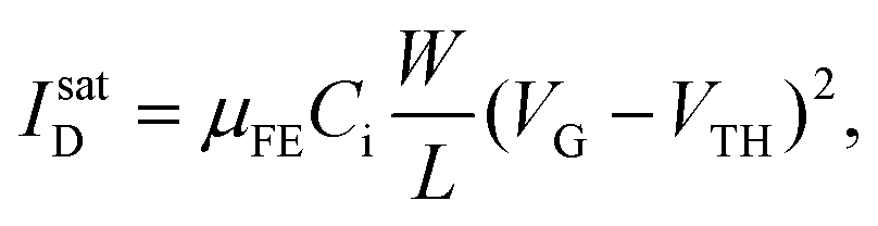 | (1) |
 | (2) |
 | ||
| Fig. 1 (a) The output characteristics from a pristine IDT-BT WG-TFT. At drain voltages beyond −0.4 V, the current is in the saturated regime for gate voltages up to at least −0.6 V. (b) A transfer characteristic from a IDT-BT WG-TFT as well as a simple drawing of the device structure. The on/off ratio is around 1000 with a relatively narrow voltage sweep range. | ||
At low gate voltages, the device operates in the subthreshold regime, where the source–drain current increases exponentially. The slope of a fit to the logarithm of ID in this region is defined as the subthreshold slope (SS). It is a measure of how quickly the device turns on and can be used to roughly estimate the effective trap density Neff, consisting of both interface and bulk traps, through
 | (3) |
The onset voltage VON is generally defined as the point where said fit intersects the off-current, or the noise level of the current. Like the threshold voltage it is a measure of when the device turns on, but VON is affected by factors affecting the measured off-current, such as doping and measurement settings. Therefore we will only use the threshold voltage in this work.
Fig. 2 illustrates fitting the square root and logarithm of ID with a line of the form y = A + Bx in order to extract the figures of merit. This process is automated using a Python script capable of identifying the linear part of the curve in question.
 | ||
| Fig. 2 Examples of fitting a linear function to the square root of the drain current, (a), to extract the field-effect mobility in the saturated regime and threshold voltage, and to the logarithm of the drain current, (b), to extract the subthreshold slope and onset voltage. | ||
The electric double layers at the gate and semiconductor surfaces act as capacitors connected in series, and so the total capacitance is given by  . As the gate electrode is significantly larger than the channel area, Cgate ≫ Cosc and thus
 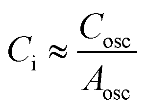 . This leads to a device configuration that is sensitive to changes in the semiconductor capacitance, and insensitive to changes in the gate capacitance.7 Instead, we are sensitive to any work function changes on the gate electrode, but not to work function changes on the semiconductor surface. Eqn (1) can then be rewritten as
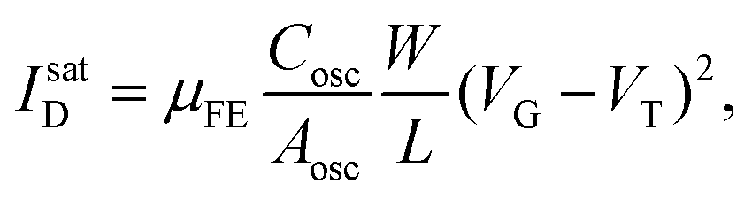 | (4) |
3 Results and discussion
3.1 The measurement protocols and C–V measurements
Before discussing the results in detail, we describe the different measurement protocols used and the purpose of each.Fig. 3, illustrates the measurement scheme used for the majority of the electrical measurements. It employs alternating periods of high stress (constant bias stress) and low stress (no applied bias) for around 220 minutes at a time. Throughout, the device figures of merit are probed using transfer measurements at two minute intervals. This can also be seen as a cycle consisting of a transfer measurement and 120 seconds of high/low stress, alternating between high and low every 100 cycles. Thus, any bias stress-induced effects will be larger during periods of high stress, while environmental effects will occur during both high and low stress.
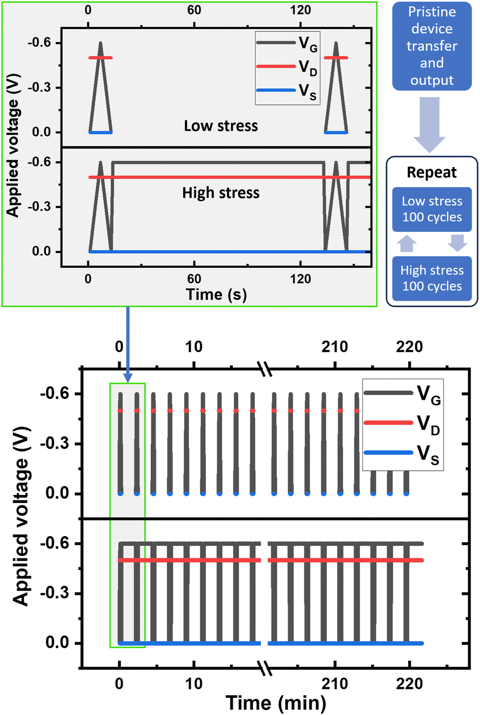 | ||
| Fig. 3 The alternating high/low stress measurement protocol. Transfer measurements are conducted every 122 seconds of high or low stress. After 100 transfer measurements and around 220 minutes, the scheme switches from high stress to low stress or vice versa. | ||
In total, the IDT-BT EGOFET was studied for 12 days, with the evolution of the current over time shown in Fig. 4. Three different measurement protocols, indicated using colors in the figure, were employed to probe different aspects of operational stability and elucidate degradation mechanisms in the device.
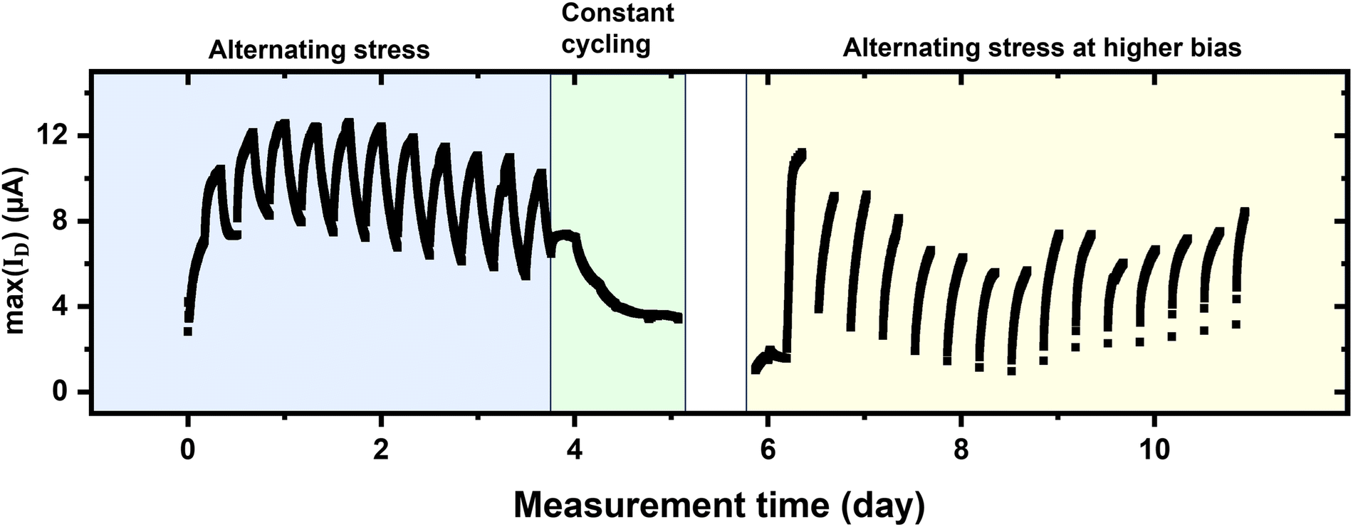 | ||
| Fig. 4 Evolution of the transfer measurement source–drain current over the whole measurement series. The colors indicate different measurement protocols followed to probe specific device properties. | ||
The first protocol employs the exact scheme pictured in Fig. 3. This allows us to study electrical stress-dependent doping and de-doping, as well as charge trap generation and annihilation in the semiconductor. This set of measurements was repeated for a second device, indentically prepared but from a different batch, to confirm the observed behavior. The data from the second device is included in S3 (ESI†).
The second protocol consists of only transfer measurements, with either no delay or a 30 second delay between measurements during which no bias is applied. This is similar to the usage an EGOFET would be subjected to in a biosensor setting.
The third protocol, started after a longer rest period of 19 hours, again uses the scheme in Fig. 3, but with the constant bias stress at −0.8 V instead of −0.6 V in order to accelerate any current or bias-induced degradation. Still, gate voltage is kept at a level where no obvious electrochemical effects could be seen in the gate leakage current.
After these measurements, with the EGOFET still in good working condition, the first protocol was repeated, this time including capacitance–voltage (C–V) measurements after each period of high and low stress. As seen in Fig. 5, the semiconductor capacitance Cosc, extracted as the capacitance saturates at VG = −0.6 V, remains unchanged at Cosc = 18 nF. This gives Ci = 8.8 μF cm−2, in line with reported values for electrolyte-gated devices.46,47 Additionally, we observe the characteristic doping shoulder in the depletion region capacitance, caused by the AC response of the additional charge carriers.42
 | ||
| Fig. 5 Capacitance–voltage characteristics recorded immediately after high and low stress measurements. The shoulder in the depletion region of the sweep is characteristic of doping in transistors. The effective gate capacitance, which is extracted as the capacitance saturates in the accumulation region, shows no difference between high and low stress measurments. | ||
Fig. 6 shows the first transfer measurement on the pristine EGOFET, transfer measurements gathered after periods of low and high stress as well as the first measurement after the device was left resting in the dark for 19 hours between the second protocol ending and the third starting. Additional transfer curves are included in S4 (ESI†). The transfer measurements show the typical characteristics of doping, with an increase in mobility accompanied by a large increase in off-current with increasing doping.19,42 The changes in threshold voltage and subthreshold slope that are readily measurable after fitting the data are impossible to spot by eye in the transfer curves. It is also worth noting that we could not observe any hysteresis in the transfer characteristics at any stage of the work. This indicates that measurements are performed at a slow enough sweep rate that we remain in quasi equilibrium at each applied gate voltage also at the higher trap densities.
 | ||
| Fig. 6 Transfer curves showing the difference between the pristine EGOFET and the lower and higher doping states. The measurements labeled “After low stress” and “After high stress” are transfer cycles 900 and 1000, while the “pristine” curve is the first transfer measurement on the fresh device. Between the second and third measurement protocol, the device was allowed to completely rest in the dark for 19 hours before measurements were resumed and the “After 19 h rest” measurement was recorded. | ||
3.2 Alternating stress measurements
After recording the output and transfer characteristics in Fig. 1a, the stability measurement protocol described in the previous section was repeated 22.5 times for a total of 2250 transfer cycles and a cumulative 2633 minutes (ca. 44 hours) under bias over a total duration of approximately 88 hours. The figures-of merit extracted from transfer measurements are shown in Fig. 7. During the initial period of low stress, the current is seen to increase after which it assumes a pattern of increasing during high stress periods and decreasing during low stress periods. The change in current is accompanied by a near identical pattern for μCi, showing that this figure of merit dominates the behavior of the max(ID). As the effective gate capacitance has been observed to not change between high and low stress measurements, we can be confident that the behavior of μCi is consistent with that of the field-effect mobility. Thus, the max(ID) behavior is entirely dominated by doping. As IDT-BT is known to undergo oxygen doping even at ppm levels of molecular oxygen,19,30 this is likely the mechanism here as well. Using the previously calculated value for Ci, we arrive at a field effect mobility on the order of 1–4 × 10⁻³ cm2 V−1 s−1. This is significantly lower than for the best reported IDT-BT OFETs but similar to other reported numbers on EGOFETs.1,22 | ||
| Fig. 7 Evolution of the figures of merit during 2250 transfer cycles and four days of EGOFET operation. During high stress, the device is biased with VD = −0.5 V and VG = −0.6 V for 120 seconds between each transfer measurement, while during low stress no bias is applied for the same duration between transfer measurements. Doping occurs during high stress and is reversed during low stress. A slower shift in threshold voltage and mobility can also be observed. | ||
The threshold voltage, VTH, shifts toward more negative values during high stress and return during low stress, with the difference in threshold voltage between the final measurements of each period being around 25 mV. The subthreshold slope, SS shifts toward higher values during high stress. The changes in threshold voltage and subthreshold slope both indicate the formation of deeper lying states in the DOS according to eqn (2) and (3). Earlier studies observing bias-induced trap generation in IDT-BT OFETs show the same kind of changes in threshold voltage and subthreshold slope that we observe.25,30,40 In the water-gated device, however, the effect on figures of merit is gradual enough that it would hardly be noticeable without the kind of longer measurement protocols we employ here. As with the doping, the increase in trap density during biasing is reversed during rest, but the effect of the trap density changes on the on-current is small compared to the effect from doping. If most of the generated trap states are deep in the trap DOS, they will have very little effect on the mobility once they are filled and the quasi Fermi level sits closer to the band edge and what we observe is expected. Still, the increase in trap density cannot be ignored as it leads to shifts in the threshold voltage, which is the figure of merit EGOFET-based biosensors rely on to detect sensing events.
In conventional OFETs, trap generation is in general dominated by states in the dielectric or at the semiconductor/dielectric interface.15,21 As the EGOFET in principle cannot have these traps, we only observe trap generation related to the semiconductor itself, explaining the much smaller effects on VTH compared to conventional devices as well as the negligible hysteresis throughout measurements.48 Water has been observed to cause traps inside IDT-BT itself. One proposed mechanism involves water molecules penetrating nanovoids in the semiconductor, where they interact with the molecule backbone, leading to bias-induced and reversible trapping while water is present in the film.19,30 As even small concentrations of water vapor present during device manufacturing has been shown to lead to these bias-induced traps, we should expect them to be a factor when operating the semiconductor submerged in water. A recent work extends the theory to direct protonation of IDT-BT in the presence of water as a cause for deep trap generation; an effect shown to be both bias induced and reversible and thus also entirely consistent with what we observe here.20
Throughout the measurements, a gradual shift in μCi and threshold voltage can also be seen. After the initial measurements, the shift is near linear and seen in both the high and low stress measurements. Water evaporation leading to less of the gate electrode being submerged, thus reducing capacitance, can be excluded as the evaporation rate is low with a lid on the reservoir. Additionally, employing a large gate area compared to channel area makes the source–drain current very insensitive to the gate double-layer capacitance.7 On the other hand, it is sensitive to the semiconductor double-layer capacitance, and so surface degradation of IDT-BT may be causing a long-term decrease in capacitance leading to a decreasing μCi. A reduction in capacitance would lead to a lower surface potential at the semiconductor, effectively decreasing the bias stress and thus simultaneously reducing the trap generation that is responsible for shifting VTH to more negative values. Any conclusive evidence for this, however, remains firmly outside the scope of this work.
3.3 Constant cycling
Immediately following the alternating high/low stress measurements, the protocol was changed to constantly cycle transfer measurements with no delay in between. This was done for approximately six hours resulting in 1372 transfer measurements. After this, a delay of 30 seconds was added between transfer measurements and measurements continued for another 2000 cycles over 25 hours. The figures of merit are shown in Fig. 8. During constant cycling the EGOFET stabilized over around 100 cycles before the figures of merit become fairly stable. As discussed earlier, the most important parameter for biosensors is stability and the main figures of merit to monitor with our device geometry is the threshold voltage, as sensing events directly translate to shifts in threshold voltage.6,8,26 During the whole period of constant cycling the shift in threshold voltage was less than 5 mV, and for four hours it stayed below 2 mV. | ||
| Fig. 8 Evolution of the figures of merit during periods of transfer cycling with no delay and 30 second delay (rest) between measurements. The figures of merit become fairly stable as doping and de-doping is in equilibrium. | ||
The other figures of merit also stabilized to a constant value, indicating doping and de-doping as well as trap generation and annihilation being in equilibrium. As expected, we observe a shift towards a new equilibrium upon adding a 30 second delay between measurements as can be seen in Fig. 8. The new equilibrium corresponds to a lower level of oxygen doping as well as a lower number of traps. This, however, happened more slowly. With an even longer delay between measurements, the equilibrium would be still closer to the pristine device case.
After these measurements, the EGOFET was left to rest, still in the dark, for 19 hours.
3.4 Alternating stress at larger gate bias
Following the rest period, the alternating high/low measurements were resumed with the gate bias under high stress increased from −0.6 V to −0.8 V. The main figures of merit extracted from these measurements are shown in Fig. 9. Due to a setup error, transfer measurements were not collected for the entire low stress periods. Nonetheless, the figures of merit from the high stress periods allow us to interpret the data. | ||
| Fig. 9 Figures of merits gathered during seven days and 4400 high/low stress cycles. During bias stress, the gate voltage was set to −0.8 V compared to the earlier −0.6 V. The difference between high and low stress values for the threshold voltage and subthreshold slope are larger at the increased gate bias. | ||
Upon starting the measurements, the transistor is fairly stable during low stress. Transitioning to high stress increases μCi by a factor of eight, indicating doping again is occurring. After two days of measurement, and thus around 24 hours under the higher bias, the high-stress value of μCi has fallen to around 40% of the maximum value attained in the beginning. Throughout the measurements, largely the same behavior is seen as during earlier measurements, with increased doping during stress and de-doping during rest. The behavior of the max(ID) is still dominated by the mobility, and the earlier trend of decreasing mobility continues until around cycle 8000.
For the threshold voltage, the difference between high and low stress values is higher than in the low stress case, at most around 50 mV compared to 25 mV, indicating the increased bias leads to more trap generation. Additionally, the consistent long-term shift in threshold voltage is steeper. The subthreshold slope during high stress is significantly higher than for earlier measurements; further indication that many more charge trap states are formed under the higher gate voltage. As the subthreshold slope sees a small increase throughout measurements, even though the source–drain current decreases by around half, it can be surmised that bias stress rather than current flow indeed is responsible for the degradation. During rest, the subthreshold slope reverts to the same values as during the earlier low stress measurements seen in Fig. 7.
The measurements show that trap generation is greatly affected by increasing the gate bias, with a larger difference between low and high stress values for both threshold voltage and subthreshold slope compared to the lower bias case. The level of doping is more difficult to infer, but the difference in max(ID) as well as mobility between high and low stress is very similar here as during the first protocol, indicating the doping rate is similar even at the elevated bias. Thus, one strategy to suppress bias-induced trap generation while retaining the increased mobility from doping could be to reduce the maximum gate bias during measurements.
4 Conclusion
We have studied the short and medium-term operational stability of an IDT-BT based EGOFET. We were able to highlight reversible doping as the main factor affecting the on-current of the transistor during operation. Under bias, the device undergoes very gradual doping that is reversed during rest. Oxygen doping is the most likely candidate as it has been widely reported in several different organic semiconductors, including IDT-BT. A future study involving gas purged electrolytes in a flow-cell setup could be helpful for clarifying this.Additionally, we observe trap generation in the semiconductor, consistent with water-induced charge traps. While these traps affect the on-current very little, they have significant enough influence on the threshold voltage that they need to be accounted for in any biosensor design based on IDT-BT.
Finally, we have showed that while both doping and charge trap generation may lead to an unstable transistor, the effects can be largely mitigated with suitable measurement protocols. Operating the device so that both doping/de-doping and charge trap generation/annihilation is in equilibrium, device figures of merit can be kept stable over extended periods of time.
The work shows that while IDT-BT is suitable for use in EGOFET-based biosensors, showing good performance and negligible hysteresis even after prolonged use, stress-induced doping and trap generation needs to be taken into account when designing measurements. This opens up for further work in suppressing doping and water-induced traps in these devices to enhance stability, or leverage the predictable and gradual nature of the effects in memristor-like applications.
Author contributions
Axel Luukkonen: conceptualization, methodology, software, validation, formal analysis, investigation, data curation, writing – original draft preparation, visualization; Jonas Jern: methodology, validation, writing – reviewing and editing; Qiao He: resources, writing – reviewing and editing; Martin Heeney: resources, writing – reviewing and editing; Ronald Österbacka: conceptualization, resources, writing – reviewing and editing, supervision, project administration, funding acquisition.Data availability
All data included in this work are available upon request by contact with the corresponding author.Conflicts of interest
There are no conflicts to declare.Acknowledgements
Financial support from the Åbo Akademi University CoE “Bioelectronic activation of cell functions” and Åbo Akademi Doctoral Network in Materials Research are acknowledged.Notes and references
- L. Kergoat, L. Herlogsson, D. Braga, B. Piro, M.-C. Pham, X. Crispin, M. Berggren and G. Horowitz, Adv. Mater., 2010, 22, 2565–2569 CrossRef CAS PubMed.
- L. Kergoat, L. Herlogsson, B. Piro, M. C. Pham, G. Horowitz, X. Crispin and M. Berggren, Proc. Natl. Acad. Sci. U. S. A., 2012, 109, 8394–8399 CrossRef CAS PubMed.
- S. H. Kim, K. Hong, W. Xie, K. H. Lee, S. Zhang, T. P. Lodge and C. D. Frisbie, Adv. Mater., 2013, 25, 1822–1846 CrossRef CAS PubMed.
- F. Zare Bidoky, W. J. Hyun, D. Song and C. D. Frisbie, Appl. Phys. Lett., 2018, 113, 053301 CrossRef.
- M. Nikolka, D. Simatos, A. Foudeh, R. Pfattner, I. McCulloch and Z. Bao, ACS Appl. Mater. Interfaces, 2020, 12, 40581–40589 CrossRef CAS PubMed.
- D. Wang, V. Noël and B. Piro, Electronics, 2016, 5, 9 CrossRef.
- R. A. Picca, K. Manoli, E. Macchia, L. Sarcina, C. D. Franco, N. Cioffi, D. Blasi, R. Österbacka, F. Torricelli, G. Scamarcio and L. Torsi, Adv. Funct. Mater., 2020, 30, 1904513 CrossRef CAS.
- E. Macchia, K. Manoli, B. Holzer, C. D. Franco, M. Ghittorelli, F. Torricelli, D. Alberga, G. F. Mangiatordi, G. Palazzo, G. Scamarcio and L. Torsi, Nat. Commun., 2018, 9, 3223 CrossRef PubMed.
- C. Sun, Y.-X. Wang, M. Sun, Y. Zou, C. Zhang, S. Cheng and W. Hu, Biosens. Bioelectron., 2020, 164, 112251 CrossRef CAS PubMed.
- M. Berto, C. Diacci, R. D'Agata, M. Pinti, E. Bianchini, M. D. Lauro, S. Casalini, A. Cossarizza, M. Berggren, D. Simon, G. Spoto, F. Biscarini and C. A. Bortolotti, Adv. Biosyst., 2018, 2, 1700072 CrossRef.
- H. Sirringhaus, Adv. Mater., 2014, 26, 1319–1335 CrossRef CAS PubMed.
- Y. Yan, Y. Zhao and Y. Liu, J. Polym. Sci., 2022, 60, 311–327 CrossRef CAS.
- R. A. Picca, K. Manoli, E. Macchia, A. Tricase, C. Di Franco, G. Scamarcio, N. Cioffi and L. Torsi, Front. Chem., 2019, 7, 667 CrossRef CAS PubMed.
- H. Sirringhaus, Adv. Mater., 2009, 21, 3859–3873 CrossRef CAS.
- P. A. Bobbert, A. Sharma, S. G. J. Mathijssen, M. Kemerink and D. M. D. Leeuw, Adv. Mater., 2012, 24, 1146–1158 CrossRef CAS PubMed.
- H. L. Gomes, P. Stallinga, F. Dinelli, M. Murgia, F. Biscarini, D. M. de Leeuw, M. Muccini and K. Müllen, Polym. Adv. Technol., 2005, 16, 227–231 CrossRef CAS.
- J. Kim, J. Jang, K. Kim, H. Kim, S. H. Kim and C. E. Park, Adv. Mater., 2014, 26, 7241–7246 CrossRef CAS PubMed.
- M. Kettner, Z. Mi, D. Kälblein, J. Brill, P. W. M. Blom and R. T. Weitz, Adv. Electron. Mater., 2019, 5, 1900295 CrossRef CAS.
- I. Dobryden, V. V. Korolkov, V. Lemaur, M. Waldrip, H.-I. Un, D. Simatos, L. J. Spalek, O. D. Jurchescu, Y. Olivier, P. M. Claesson and D. Venkateshvaran, Nat. Commun., 2022, 13, 3076 CrossRef CAS PubMed.
- S. Park, W. Choi, S. H. Kim, H. Lee and K. Cho, Adv. Mater., 2023, 35, 2303707 CrossRef CAS PubMed.
- H. F. Haneef, A. M. Zeidell and O. D. Jurchescu, J. Mater. Chem. C, 2020, 8, 759–787 RSC.
- H. F. Iqbal, Q. Ai, K. J. Thorley, H. Chen, I. McCulloch, C. Risko, J. E. Anthony and O. D. Jurchescu, Nat. Commun., 2021, 12, 2352 CrossRef CAS PubMed.
- D. Blasi, F. Viola, F. Modena, A. Luukkonen, E. Macchia, R. A. Picca, Z. Gounani, A. Tewari, R. Österbacka, M. Caironi, Z. M. K. Vajna, G. Scamarcio, F. Torricelli and L. Torsi, J. Mater. Chem. C, 2020, 8, 15312–15321 RSC.
- E. J. W. List-Kratochvil, G. Ligorio, H. J. N. P. D. Mello, S. Dalgleish and M. Mulato, Organic and Hybrid Sensors and Bioelectronics XI, San Diego, United States, 2018, p. 45 Search PubMed.
- A. Doumbia, J. Tong, R. J. Wilson and M. L. Turner, Adv. Electron. Mater., 2021, 7, 2100071 CrossRef CAS.
- F. Torricelli, D. Z. Adrahtas, Z. Bao, M. Berggren, F. Biscarini, A. Bonfiglio, C. A. Bortolotti, C. D. Frisbie, E. Macchia, G. G. Malliaras, I. McCulloch, M. Moser, T.-Q. Nguyen, R. M. Owens, A. Salleo, A. Spanu and L. Torsi, Nat. Rev. Methods Primers, 2021, 1, 66 CrossRef CAS PubMed.
- A. Luukkonen, A. Tewari, K. Björkström, A. M. Ghafari, E. Macchia, F. Torricelli, L. Torsi and R. Österbacka, Org. Electron., 2023, 120, 106844 CrossRef CAS.
- X. Zhang, H. Bronstein, A. J. Kronemeijer, J. Smith, Y. Kim, R. J. Kline, L. J. Richter, T. D. Anthopoulos, H. Sirringhaus, K. Song, M. Heeney, W. Zhang, I. McCulloch and D. M. DeLongchamp, Nat. Commun., 2013, 4, 2238 CrossRef PubMed.
- H. Makki, C. A. Burke and A. Troisi, J. Phys. Chem. Lett., 2023, 14, 8867–8873 CrossRef CAS PubMed.
- M. Nikolka, I. Nasrallah, B. Rose, M. K. Ravva, K. Broch, A. Sadhanala, D. Harkin, J. Charmet, M. Hurhangee, A. Brown, S. Illig, P. Too, J. Jongman, I. McCulloch, J.-L. Bredas and H. Sirringhaus, Nat. Mater., 2017, 16, 356–362 CrossRef CAS PubMed.
- Y. Zheng, G. N. Wang, J. Kang, M. Nikolka, H. Wu, H. Tran, S. Zhang, H. Yan, H. Chen, P. Y. Yuen, J. Mun, R. H. Dauskardt, I. McCulloch, J. B. Tok, X. Gu and Z. Bao, Adv. Funct. Mater., 2019, 29, 1905340 CrossRef CAS.
- W. Zhang, J. Smith, S. E. Watkins, R. Gysel, M. McGehee, A. Salleo, J. Kirkpatrick, S. Ashraf, T. Anthopoulos, M. Heeney and I. McCulloch, J. Am. Chem. Soc., 2010, 132, 11437–11439 CrossRef CAS PubMed.
- Z. A. Lamport, K. J. Barth, H. Lee, E. Gann, S. Engmann, H. Chen, M. Guthold, I. McCulloch, J. E. Anthony, L. J. Richter, D. M. DeLongchamp and O. D. Jurchescu, Nat. Commun., 2018, 9, 5130 CrossRef PubMed.
- C. Liu, Y. Xu and Y.-Y. Noh, Mater. Today, 2015, 18, 79–96 CrossRef CAS.
- D. Boudinet, M. Benwadih, Y. Qi, S. Altazin, J.-M. Verilhac, M. Kroger, C. Serbutoviez, R. Gwoziecki, R. Coppard, G. Le Blevennec, A. Kahn and G. Horowitz, Org. Electron., 2010, 11, 227–237 CrossRef CAS.
- D. Venkateshvaran, M. Nikolka, A. Sadhanala, V. Lemaur, M. Zelazny, M. Kepa, M. Hurhangee, A. J. Kronemeijer, V. Pecunia, I. Nasrallah, I. Romanov, K. Broch, I. McCulloch, D. Emin, Y. Olivier, J. Cornil, D. Beljonne and H. Sirringhaus, Nature, 2014, 515, 384–388 CrossRef CAS PubMed.
- D. Simatos, M. Nikolka, J. Charmet, L. J. Spalek, Z. Toprakcioglu, I. E. Jacobs, I. B. Dimov, G. Schweicher, M. J. Lee, C. M. Fernández-Posada, D. J. Howe, T. A. Hakala, L. W. Y. Roode, V. Pecunia, T. P. Sharp, W. Zhang, M. Alsufyani, I. McCulloch, T. P. J. Knowles and H. Sirringhaus, SmartMat, 2024, e1291 CrossRef CAS.
- I. Holzer, V. Lemaur, M. Wang, H.-Y. Wu, L. Zhang, R. Marcial-Hernandez, P. Gilhooly-Finn, P. Cavassin, S. Hoyas, D. Meli, R. Wu, B. D. Paulsen, J. Strzalka, A. Liscio, J. Rivnay, H. Sirringhaus, N. Banerji, D. Beljonne, S. Fabiano and C. B. Nielsen, J. Mater. Chem. C, 2024, 12, 3686–3697 RSC.
- A. Al Baroot, A. Alshammari and M. Grell, Thin Solid Films, 2019, 669, 665–669 CrossRef CAS.
- H. F. Iqbal, M. Waldrip, H. Chen, I. McCulloch and O. D. Jurchescu, Adv. Electron. Mater., 2021, 7, 2100393 CrossRef CAS.
- H. Bronstein, D. S. Leem, R. Hamilton, P. Woebkenberg, S. King, W. Zhang, R. S. Ashraf, M. Heeney, T. D. Anthopoulos, J. D. Mello and I. McCulloch, Macromolecules, 2011, 44, 6649–6652 CrossRef CAS.
- D. K. Schroder, Semiconductor Material and Device Characterization, Wiley, 1st edn, 2005 Search PubMed.
- M. C. J. M. Vissenberg and M. Matters, Phys. Rev. B:Condens. Matter Mater. Phys., 1998, 57, 12964–12967 CrossRef CAS.
- M. Grünewald, P. Thomas and D. Würtz, Phys. Status Solidi B, 1980, 100, K139–K143 CrossRef.
- W. L. Kalb and B. Batlogg, Phys. Rev. B:Condens. Matter Mater. Phys., 2010, 81, 035327 CrossRef.
- T. Cramer, A. Kyndiah, M. Murgia, F. Leonardi, S. Casalini and F. Biscarini, Appl. Phys. Lett., 2012, 100, 143302 CrossRef.
- T. Cramer, A. Campana, F. Leonardi, S. Casalini, A. Kyndiah, M. Murgia and F. Biscarini, J. Mater. Chem. B, 2013, 1, 3728 RSC.
- M. Egginger, S. Bauer, R. Schwödiauer, H. Neugebauer and N. S. Sariciftci, Monatsh. Chem., 2009, 140, 735–750 CrossRef CAS.
Footnote |
| † Electronic supplementary information (ESI) available. See DOI: https://doi.org/10.1039/d4tc04100c |
| This journal is © The Royal Society of Chemistry 2025 |